msp430 programming via the bootstrap loader (bsl) (rev. b) filemsp430 programming via the bootstrap...
TRANSCRIPT
MSP430 Programming Via the Bootstrap Loader
User's Guide
Literature Number: SLAU319B
July 2010–Revised March 2012
Contents
1 Programming With the Bootstrap Loader ............................................................................... 51.1 Supplementary Online Information ....................................................................................... 51.2 Introduction .................................................................................................................. 51.3 Standard RESET and BSL Entry Sequence ............................................................................ 6
1.3.1 MSP430 Devices With Shared JTAG Pins ..................................................................... 61.3.2 MSP430 Flash Devices With Dedicated JTAG Pins .......................................................... 71.3.3 Devices With USB ................................................................................................. 7
1.4 UART Protocol .............................................................................................................. 71.5 USB Protocol ................................................................................................................ 7
2 ROM-Based Bootstrap Loader Protocol ................................................................................. 92.1 Synchronization Sequence ................................................................................................ 92.2 Commands ................................................................................................................... 9
2.2.1 Unprotected Commands .......................................................................................... 92.2.2 Password Protected Commands ................................................................................. 9
2.3 Programming Flow ........................................................................................................ 102.4 Data Frame ................................................................................................................. 11
2.4.1 Data-Stream Structure ........................................................................................... 112.4.2 Checksum ......................................................................................................... 122.4.3 Example Sequence ............................................................................................... 122.4.4 Commands – Detailed Description ............................................................................. 12
2.5 Loadable BSL .............................................................................................................. 162.6 Exiting the BSL ............................................................................................................ 172.7 Password Protection ...................................................................................................... 172.8 Code Protection Fuse ..................................................................................................... 182.9 BSL Internal Settings and Resources .................................................................................. 18
2.9.1 Chip Identification and BSL Version ........................................................................... 182.9.2 Vectors to Call the BSL Externally ............................................................................. 182.9.3 Initialization Status ............................................................................................... 192.9.4 Memory Allocation and Resources ............................................................................. 20
3 Flash-Based Bootstrap Loader Protocol ............................................................................... 213.1 BSL Data Packet .......................................................................................................... 213.2 UART Peripheral Interface (PI) .......................................................................................... 21
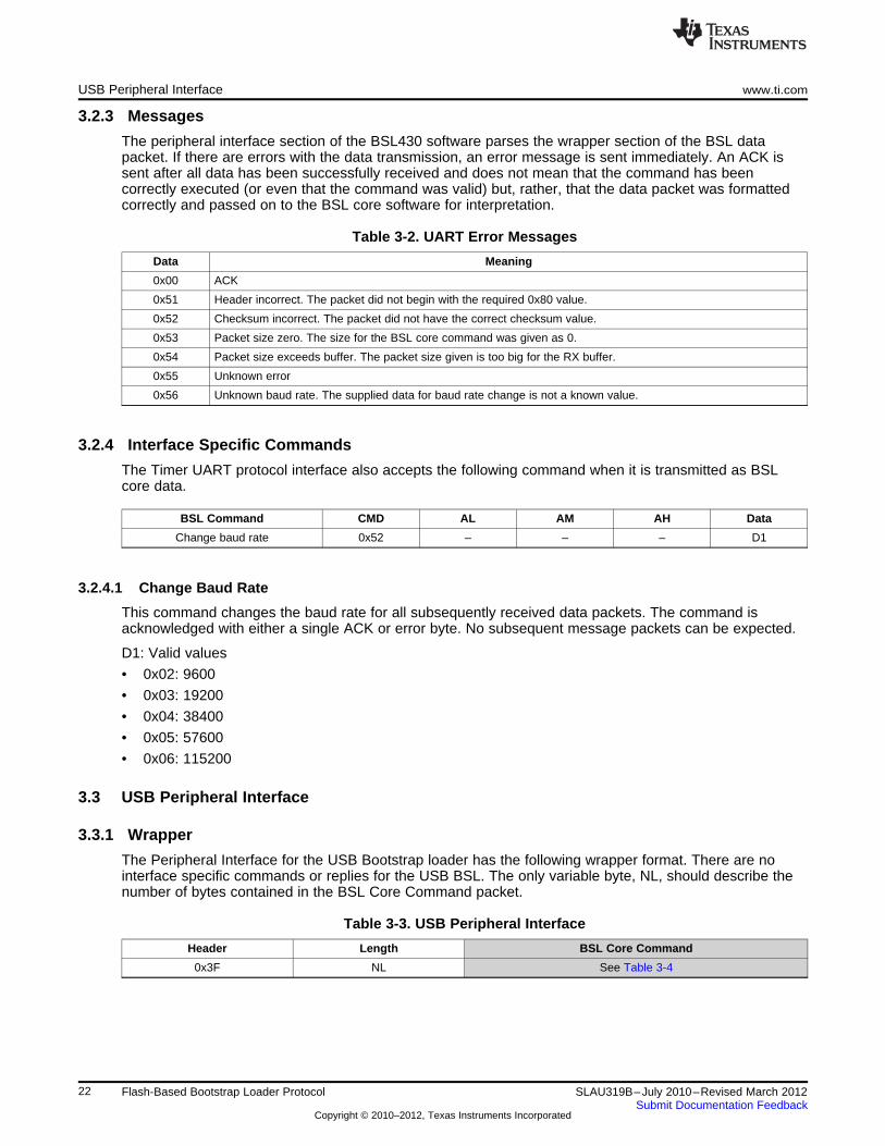
3.2.1 Wrapper ............................................................................................................ 213.2.2 Abbreviations ...................................................................................................... 213.2.3 Messages .......................................................................................................... 223.2.4 Interface Specific Commands ................................................................................... 22
3.3 USB Peripheral Interface ................................................................................................. 223.3.1 Wrapper ............................................................................................................ 223.3.2 Hardware Requirements ......................................................................................... 23
3.4 BSL Core Command Structure .......................................................................................... 233.4.1 Abbreviations ...................................................................................................... 233.4.2 Command Descriptions .......................................................................................... 24
3.5 BSL Security ............................................................................................................... 253.5.1 Protected Commands ............................................................................................ 253.5.2 RAM Erase ........................................................................................................ 25
2 Contents SLAU319B–July 2010–Revised March 2012Submit Documentation Feedback
Copyright © 2010–2012, Texas Instruments Incorporated
www.ti.com
3.6 BSL Core Responses ..................................................................................................... 263.6.1 Abbreviations ...................................................................................................... 263.6.2 BSL Core Messages ............................................................................................. 273.6.3 BSL Version Number ............................................................................................. 273.6.4 Example Sequences for UART BSL ........................................................................... 28
3.7 BSL Public Functions and Z-Area ....................................................................................... 283.7.1 Starting the BSL From an External Application ............................................................... 283.7.2 Function Description ............................................................................................. 28
4 Bootstrap Loader Hardware ................................................................................................ 294.1 Hardware Description ..................................................................................................... 29
4.1.1 Power Supply ..................................................................................................... 294.1.2 Serial Interface .................................................................................................... 304.1.3 Target Connector ................................................................................................. 314.1.4 Parts List ........................................................................................................... 32
5 Differences Between Devices and Bootstrap Loader Versions ................................................ 335.1 5xx and 6xx BSL Versions ............................................................................................... 335.2 Special Consideration for ROM BSL Version 1.10 .................................................................... 345.3 ROM BSL Known Issues ................................................................................................. 345.4 Special Note on the MSP430F14x Device Family BSL .............................................................. 42
6 Bootstrap Loader PCB Layout Suggestion ........................................................................... 43
Revision History ......................................................................................................................... 46
3SLAU319B–July 2010–Revised March 2012 ContentsSubmit Documentation Feedback
Copyright © 2010–2012, Texas Instruments Incorporated
www.ti.com
List of Figures
1-1. Standard RESET Sequence............................................................................................... 6
1-2. BSL Entry Sequence at Shared JTAG Pins ............................................................................. 6
1-3. BSL Entry Sequence at Dedicated JTAG Pins.......................................................................... 7
4-1. Bootstrap Loader Interface Schematic ................................................................................. 29
6-1. Universal BSL Interface PCB Layout, Top ............................................................................. 43
6-2. Universal BSL Interface PCB Layout, Bottom ......................................................................... 43
6-3. Universal BSL Interface Component Placement ...................................................................... 44
6-4. Universal BSL Interface Component Placement ...................................................................... 45
List of Tables
2-1. Data Frame of BSL Commands ........................................................................................ 11
2-2. Recommendations for MSP430F149 [F449] (TA = 25°C, VCC = 3.0 V, fmax = 6.7 MHz)........................... 15
2-3. Recommendations for MSP430F2131 (TA = 25°C, VCC = 3.0 V, fmax = 6.7 MHz) .................................. 15
3-1. UART Protocol Interface.................................................................................................. 21
3-2. UART Error Messages.................................................................................................... 22
3-3. USB Peripheral Interface ................................................................................................. 22
3-4. BSL Core Commands..................................................................................................... 23
3-5. BSL Core Responses ..................................................................................................... 26
3-6. BSL Core Messages ...................................................................................................... 27
4-1. Serial-Port Signals and Pin Assignments .............................................................................. 30
4-2. RS-232 Levels ............................................................................................................. 30
4-3. Pin Assignment of Target Connector .................................................................................. 31
4-4. Universal BSL Interface Parts List ...................................................................................... 32
5-1. BSL Version 1.10 on F13x, F14x(1) (excluding Rev AA), F11x, and F11x1 ...................................... 35
5-2. BSL Version 1.30 on F41x, F11x, and F11x1 ......................................................................... 36
5-3. BSL Version 1.40 on F12x ............................................................................................... 37
5-4. BSL Version 1.60 on F11x2, F12x2, F43x, F44x, FE42x, FW42x, F(G)43x, F415, F417 ....................... 38
5-5. BSL Version 1.61 on F16x, F161x, F42x0, F13x rev AA, F14x(1) rev AA......................................... 39
5-6. BSL Version 2.02 on F21xx, F22xx, F24x, F23x ...................................................................... 40
5-7. BSL Version 2.12 and 2.13 on FG46xx, F261x, F471xx ............................................................ 41
4 List of Figures SLAU319B–July 2010–Revised March 2012Submit Documentation Feedback
Copyright © 2010–2012, Texas Instruments Incorporated
Chapter 1SLAU319B–July 2010–Revised March 2012
Programming With the Bootstrap Loader
The MSP430™ BSL enables users to communicate with embedded memory in the MSP430microcontroller during the prototyping phase, final production, and in service. Both the programmablememory (flash memory) and the data memory (RAM) can be modified as required. Do not confuse thebootstrap loader with programs found in some digital signal processors (DSPs) that automatically loadprogram code (and data) from external memory to the internal memory of the DSP. These programs areoften referred to as bootstrap loaders as well.
To use the bootstrap loader, a specific BSL entry sequence must be applied. An added sequence ofcommands initiates the desired function. A boot-loading session can be exited by continuing operation at adefined user program address or by the reset condition.
If the device is secured by disabling JTAG, it is still possible to use the BSL. Access to the MSP430memory through the BSL is protected against misuse by a user-defined password.
1.1 Supplementary Online Information
As a compliment to this document, a BSL wiki page is available. This wiki contains links to additional BSLprojects, information, and an errata for this document. The wiki can be found athttp://processors.wiki.ti.com/index.php/BSL_(MSP430).
A zip file with additional information, executables, and code samples can be found athttp://www.ti.com/lit/zip/slau319.
1.2 Introduction
This bootstrap loader provides a method to program the flash memory during MSP430 projectdevelopment and updates. It can be activated by a utility that sends commands using the UART protocol.The BSL enables the user to control the activity of the MSP430 and to exchange data using a personalcomputer or other device.
To avoid accidental overwriting of the BSL code, this code is stored in a secure memory location, eitherROM or specially protected flash. To prevent unwanted source readout, any BSL command that directly orindirectly allows data reading is password protected.
To invoke the bootstrap loader, a BSL entry sequence must be applied to dedicated pins. After that, asynchronization character, followed by the data frame of a specific command, initiates the desiredfunction.
MSP430 is a trademark of Texas Instruments.
5SLAU319B–July 2010–Revised March 2012 Programming With the Bootstrap LoaderSubmit Documentation Feedback
Copyright © 2010–2012, Texas Instruments Incorporated
RSTDTR/NMI
( )
TEST( )RTS
User Program Starts
Bootstrap Loader Starts
RSTDTR/NMI
( )
TEST( )RTS
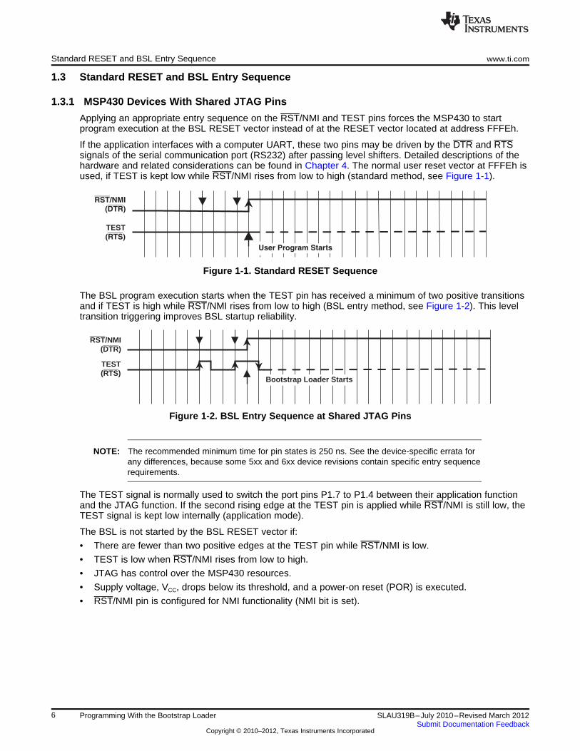
Standard RESET and BSL Entry Sequence www.ti.com
1.3 Standard RESET and BSL Entry Sequence
1.3.1 MSP430 Devices With Shared JTAG Pins
Applying an appropriate entry sequence on the RST/NMI and TEST pins forces the MSP430 to startprogram execution at the BSL RESET vector instead of at the RESET vector located at address FFFEh.
If the application interfaces with a computer UART, these two pins may be driven by the DTR and RTSsignals of the serial communication port (RS232) after passing level shifters. Detailed descriptions of thehardware and related considerations can be found in Chapter 4. The normal user reset vector at FFFEh isused, if TEST is kept low while RST/NMI rises from low to high (standard method, see Figure 1-1).
Figure 1-1. Standard RESET Sequence
The BSL program execution starts when the TEST pin has received a minimum of two positive transitionsand if TEST is high while RST/NMI rises from low to high (BSL entry method, see Figure 1-2). This leveltransition triggering improves BSL startup reliability.
Figure 1-2. BSL Entry Sequence at Shared JTAG Pins
NOTE: The recommended minimum time for pin states is 250 ns. See the device-specific errata forany differences, because some 5xx and 6xx device revisions contain specific entry sequencerequirements.
The TEST signal is normally used to switch the port pins P1.7 to P1.4 between their application functionand the JTAG function. If the second rising edge at the TEST pin is applied while RST/NMI is still low, theTEST signal is kept low internally (application mode).
The BSL is not started by the BSL RESET vector if:
• There are fewer than two positive edges at the TEST pin while RST/NMI is low.
• TEST is low when RST/NMI rises from low to high.
• JTAG has control over the MSP430 resources.
• Supply voltage, VCC, drops below its threshold, and a power-on reset (POR) is executed.
• RST/NMI pin is configured for NMI functionality (NMI bit is set).
6 Programming With the Bootstrap Loader SLAU319B–July 2010–Revised March 2012Submit Documentation Feedback
Copyright © 2010–2012, Texas Instruments Incorporated
RST
DTR
/NMI
( )
TCK
( )RTSBootstrap Loader Starts
www.ti.com UART Protocol
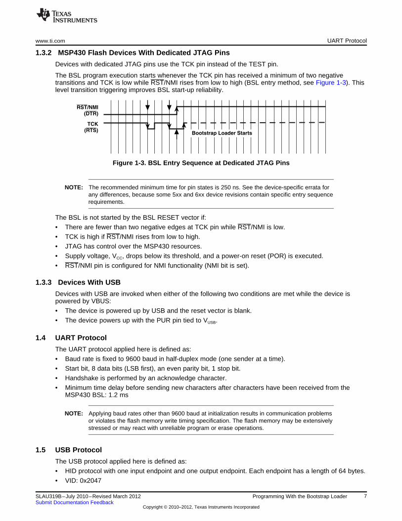
1.3.2 MSP430 Flash Devices With Dedicated JTAG Pins
Devices with dedicated JTAG pins use the TCK pin instead of the TEST pin.
The BSL program execution starts whenever the TCK pin has received a minimum of two negativetransitions and TCK is low while RST/NMI rises from low to high (BSL entry method, see Figure 1-3). Thislevel transition triggering improves BSL start-up reliability.
Figure 1-3. BSL Entry Sequence at Dedicated JTAG Pins
NOTE: The recommended minimum time for pin states is 250 ns. See the device-specific errata forany differences, because some 5xx and 6xx device revisions contain specific entry sequencerequirements.
The BSL is not started by the BSL RESET vector if:
• There are fewer than two negative edges at TCK pin while RST/NMI is low.
• TCK is high if RST/NMI rises from low to high.
• JTAG has control over the MSP430 resources.
• Supply voltage, VCC, drops below its threshold, and a power-on reset (POR) is executed.
• RST/NMI pin is configured for NMI functionality (NMI bit is set).
1.3.3 Devices With USB
Devices with USB are invoked when either of the following two conditions are met while the device ispowered by VBUS:
• The device is powered up by USB and the reset vector is blank.
• The device powers up with the PUR pin tied to VUSB.
1.4 UART Protocol
The UART protocol applied here is defined as:
• Baud rate is fixed to 9600 baud in half-duplex mode (one sender at a time).
• Start bit, 8 data bits (LSB first), an even parity bit, 1 stop bit.
• Handshake is performed by an acknowledge character.
• Minimum time delay before sending new characters after characters have been received from theMSP430 BSL: 1.2 ms
NOTE: Applying baud rates other than 9600 baud at initialization results in communication problemsor violates the flash memory write timing specification. The flash memory may be extensivelystressed or may react with unreliable program or erase operations.
1.5 USB Protocol
The USB protocol applied here is defined as:
• HID protocol with one input endpoint and one output endpoint. Each endpoint has a length of 64 bytes.
• VID: 0x2047
7SLAU319B–July 2010–Revised March 2012 Programming With the Bootstrap LoaderSubmit Documentation Feedback
Copyright © 2010–2012, Texas Instruments Incorporated
USB Protocol www.ti.com
• PID: 0x0200
8 Programming With the Bootstrap Loader SLAU319B–July 2010–Revised March 2012Submit Documentation Feedback
Copyright © 2010–2012, Texas Instruments Incorporated
Chapter 2SLAU319B–July 2010–Revised March 2012
ROM-Based Bootstrap Loader Protocol
2.1 Synchronization Sequence
Before sending any command to the BSL, a synchronization character (SYNC) with its value of 80h mustbe sent to the BSL. This character is necessary to calculate all the essential internal parameters, whichmaintain UART and flash memory program and erase timings. It provides the BSL system time reference.When this is received, an acknowledge DATA_ACK = 90h is sent back by the BSL to confirm successfulreception.
This sequence must be done before every command that is sent to the BSL.
NOTE: The synchronization character is not part of the Data Frame described in Section 2.4.
2.2 Commands
Two categories of commands are available: commands that require a password and commands that donot require a password. The password protection safeguards every command that potentially allows director indirect data access.
2.2.1 Unprotected Commands• Receive password
• Mass erase (erase entire flash memory, main as well as information memory)
• Transmit BSL version (V1.50 or higher or in loadable BL_150S_14x.txt but not V2.x BSLs)
• Change baud rate (V1.60 or V1.61 or V2.0x or in loadable BL_150S_14x.txt)
2.2.2 Password Protected Commands• Receive data block to program flash memory, RAM, or peripherals
• Transmit data block
• Erase segment
• Erase check (present in V1.60 or higher or in loadable BL_150S_14x.txt)
• Set Memory Offset (present in V2.12 or higher)
• Load program counter and start user program
• Change baud rate (BSL versions lower than V1.60 and higher than V2.10)
9SLAU319B–July 2010–Revised March 2012 ROM-Based Bootstrap Loader ProtocolSubmit Documentation Feedback
Copyright © 2010–2012, Texas Instruments Incorporated
Programming Flow www.ti.com
2.3 Programming Flow
The write access (RX data block command) to the flash memory, RAM, or peripheral modules area isexecuted online. That means a data byte or word is processed immediately after receipt, and the writecycle is finished before a following byte or word has completely arrived. Therefore, the entire write time isdetermined by the baud rate, and no buffering mechanism is necessary.
Data sections located below the flash memory area address are assumed to be loaded into the RAM orperipheral module area and, thus, no specific flash control bits are affected.
NOTE: If control over the UART protocol is lost, either by line faults or by violating the data frameconventions, the only way to recover is to rerun the BSL entry sequence to initiate anotherBSL session.
10 ROM-Based Bootstrap Loader Protocol SLAU319B–July 2010–Revised March 2012Submit Documentation Feedback
Copyright © 2010–2012, Texas Instruments Incorporated
www.ti.com Data Frame
2.4 Data Frame
To ensure high data security during the data transmission, a data frame protocol called serial standardprotocol (SSP) is used. The BSL is considered the receiver in Table 2-1.
2.4.1 Data-Stream Structure• The first eight bytes (HDR through LH) are mandatory (xx represents dummy data).
• Data bytes D1 to Dn are optional.
• Two bytes (CKL and CKH) for checksum are mandatory.
• Acknowledge done by the BSL is mandatory, except with the TX data block and TX BSL versioncommands.
Table 2-1. Data Frame of BSL Commands (1) (2) (3) (4) (5) (6)
ReceivedBSL HDR CMD L1 L2 AL AH LL LH D1 D2…Dn CKL CKH ACK
Command
RX data block 80 12 n n AL AH n–4 0 D1 D2 … Dn–4 CKL CKH ACK
RX password 80 10 24 24 xx xx xx xx D1 D2 … D20 CKL CKH ACK
Erase segment 80 16 04 04 AL AH 02 A5 – – – – CKL CKH ACK
Erase main or info 80 16 04 04 AL AH 04 A5 – – – – CKL CKH ACK
Mass erase 80 18 04 04 xx xx 06 A5 – – – – CKL CKH ACK
Erase check 80 1C 04 04 AL AH LL LH – – – – CKL CKH ACK
Change baud rate 80 20 04 04 D1 D2 D3 xx – – – – CKL CKH ACK
Set mem offset 80 21 04 04 xx xx AL AH – – – – CKL CKH ACK
Load PC 80 1A 04 04 AL AH xx xx – – – – CKL CKH ACK
TX data block 80 14 04 04 AL AH n 0 – – – – CKL CKH –
BSL responds 80 xx n n D1 D2 ... ... … ... … Dn CKL CKH –
TX BSL version 80 1E 04 04 xx xx xx xx – – – – CKL CKH –
BSL responds 80 xx 10 10 D1 D2 ... ... … … … D10 CKL CKH –(1) All numbers are bytes in hexadecimal notation.(2) ACK is sent back by the BSL.(3) The synchronization sequence is not part of the data frame.(4) The erase check and TX BSL version commands are members of the standard command set in BSLs V1.50 or higher but
excluding 2.x BSLs.(5) The change baud rate command is not a member of the standard command set (V1.60 or higher or in loadable
BL_150S_14x.txt).(6) Abbreviations:
HDR: Header. Any value between 80h and 8Fh (normally 80h).CMD: Command identificationL1, L2: Number of bytes consisting of AL through Dn. Restrictions: L1 = L2, L1 < 255, L1 evenAL, AH: Block start address or erase (check) address or jump address LO or HI byteLL, LH: Number of pure data bytes (250 max) or erase information LO or HI byte or block length of erase check (FFFFh max)D1 … Dn: Data bytesCKL, CKH: 16-bit checksum LO or HI bytexx: Can be any data–: No character (data byte) received or transmittedACK: The acknowledge character returned by the BSL. Can be either DATA_ACK = 90h: Frame was received correctly,command was executed successfully, or DATA_NAK = A0h: Frame not valid (for example, wrong checksum, L1 ≠ L2), commandis not defined, is not allowed, or was executed unsuccessfully.n: Number of bytes consisting of AL through Dn
11SLAU319B–July 2010–Revised March 2012 ROM-Based Bootstrap Loader ProtocolSubmit Documentation Feedback
Copyright © 2010–2012, Texas Instruments Incorporated

Data Frame www.ti.com
2.4.2 Checksum
The 16-bit (2-byte) checksum is calculated over all received or transmitted bytes B1...Bn in the data frame,except the checksum bytes themselves, by XORing words (two successive bytes) and inverting the result.
This means that B1 is always the HDR byte and Bn is the last data byte just before the CKL byte.
FormulaCHECKSUM = INV [ (B1 + 256 × B2) XOR (B3 + 256 × B4) XOR … XOR (Bn–1 + 256 × Bn) ]orCKL = INV [ B1 XOR B3 XOR … XOR Bn–1 ]CKH = INV [ B2 XOR B4 XOR … XOR Bn ]
2.4.3 Example Sequence
The following example shows a request to read the memory of the MSP430 from location 0x0F00. Allvalues shown below are represented in hexadecimal format.
TO BSL: 80(Synchronization character sent to the BSL)
FROM BSL: 90(Acknowledge from BSL)
TO BSL: 80 14 04 04 00 0F 0E 00 75 E0(Send Command to read memory from 0x0F00, length 0x000E)
FROM BSL: 80 00 0E 0E F2 13 40 40 00 00 00 00 00 00 02 01 01 01 C0 A2(Returned values from BSL)
2.4.4 Commands – Detailed Description
See Table 2-1.
2.4.4.1 General
Following the header byte HDR (80h) and the command identification CMD, the frame length bytes L1 andL2 (which must be equal) hold the number of bytes following L2, excluding the checksum bytes CKL andCKH.
Bytes AL, AH, LL, LH, D1...Dn are command-specific. However, the checksum bytes CKL (low byte) andCKH (high byte) are mandatory.
If the data frame has been received correctly and the command execution was successful, anacknowledge character DATA_ACK = 90h is sent back by the BSL. Incorrectly received data frames,unsuccessful operations, and commands that are locked or not defined are confirmed with a DATA_NAK =A0h.
NOTE: BSL versions lower than V1.30 support only byte-access operations. Therefore, theperipheral module addresses at 0100h to 01FFh cannot be accessed correctly, because theyare word-oriented. In version V1.30 and higher, addresses 0000h to 00FFh are accessed inbyte mode; all others are accessed in word mode.
2.4.4.2 RX Data Block
The receive data block command is used for any write access to the flash memory, RAM, or peripheralmodule control registers at 0000h to 01FFh. It is password protected.
The 16-bit even-numbered block start address is defined in AL (low byte) and AH (high byte). The 16-biteven-numbered block length is defined in LL (low byte) and LH (high byte). Because pure data bytes arelimited to a maximum of 250, LH is always 0.
12 ROM-Based Bootstrap Loader Protocol SLAU319B–July 2010–Revised March 2012Submit Documentation Feedback
Copyright © 2010–2012, Texas Instruments Incorporated

www.ti.com Data Frame
The following data bytes are succeeded by the checksum bytes CKL (low byte) and CKH (high byte). Ifthe receipt and programming of the appropriate data block was successful, an acknowledge characterDATA_ACK is sent back by the BSL. Otherwise, the BSL confirms with a DATA_NAK.
NOTE: BSL versions V1.40 and higher support online verification inside the MSP430 for addresses0200h to FFFFh, which reduces programming and verification time by 50%. Onlineverification means that the data is immediately verified with the data that is written into theflash without transmitting it again. In case of an error, the loadable bootstrap loaderBL_150S_14x.txt additionally stores the first incorrectly written location address+3 into theerror address buffer in the RAM at address 0200h (021Eh for F14x devices).
2.4.4.3 RX Password
The receive password command is used to unlock the password-protected commands, which performreading, writing, or segment-erasing memory access. It is not password protected.
Neither start address nor block length information is necessary, because the 32-byte password is alwayslocated at addresses FFE0h to FFFFh. Data bytes D1 to D20h hold the password information starting withD1 at address FFE0h.
If the receipt and verification of the password is correct, a positive acknowledge DATA_ACK is sent backby the BSL, and the password-protected commands become unlocked. Otherwise the BSL confirms with aDATA_NAK.
Once the protected commands become unlocked, they remain unlocked until another BSL entry isinitiated.
2.4.4.4 Mass Erase
The mass erase command erases the entire flash memory area (main memory plus information memory,see corresponding data sheet). It is not password protected.
All parameters shown in Table 2-1 are mandatory. After erasing, an acknowledge character DATA_ACK issent back by the BSL.
Mass erase initializes the password area to 32 times 0FFh.
NOTE: BSL versions V2.01 and higher support automatic clearing of the LOCKA bit protectinginformation flash memory. When the BSL is entered from a reset condition, LOCKA iscleared by the BSL to mass erase the flash, including information memory. When the BSL isentered in-application, user software should ensure that LOCKA is written as 1 prior toinitiating the BSL. Otherwise, information flash is not erased during a BSL mass erase.
2.4.4.5 Erase Segment
The erase segment command erases specific flash memory segments. It is password protected.
The address bytes AL (low byte) and AH (high byte) select the appropriate segment. Any even-numberedaddress within the segment to be erased is valid. After segment erasing, an acknowledge characterDATA_ACK is sent back by the BSL (V1.40 or lower).
BSL versions V1.60 or higher perform a subsequent erase check of the corresponding segment andrespond with a DATA_NAK if the erasure was not successful. In this case, the first non-erased locationaddress + 1 is stored in the error address buffer in the RAM at address 0200h (021Eh for F14x devices).In this version, a problem occurs if only one of the information memory segments is erased. In this case,an error is reported, because an automatic erase check over the whole information memory is performed.As a solution, either erase the whole information memory or do a separate erase check after the erase,even if the erase reported an error.
Erase segment 0 clears the password area and, therefore, the remaining password is 32 times 0FFh.
13SLAU319B–July 2010–Revised March 2012 ROM-Based Bootstrap Loader ProtocolSubmit Documentation Feedback
Copyright © 2010–2012, Texas Instruments Incorporated

Data Frame www.ti.com
When applying LL = 0x04 and LH = 0xA5, a mass erasure of only the main memory is performed. Indeed,this command must be executed a minimum of 12 times to achieve a total erasure time of >200 ms. Nosubsequent erase check of the entire main memory is done. Use the erase check command additionally.Check the device data sheet for more information on the cumulative (mass) erase time that must be metand the number of erase cycles required.
2.4.4.6 Erase Main or Info
The erase main or info command erases specific flash memory section. It is password protected.
The address bytes AL (low byte) and AH (high byte) select the appropriate section of flash (Main orINFO). Any even-numbered address within the section to be erased is valid.
2.4.4.7 Erase Check
The erase check command verifies the erasure of flash memory within a certain address range. It ispassword protected.
The 16-bit block start address is defined in AL (low byte) and AH (high byte). The 16-bit block length isdefined in LL (low byte) and LH (high byte). Both can be either even or odd numbered to allow oddboundary checking.
If the erase check of the appropriate data block was successful (all bytes contain 0FFh), an acknowledgecharacter DATA_ACK is sent back by the BSL. Otherwise, the BSL confirms with a DATA_NAK and thefirst non-erased location address + 1 is stored in the error address buffer at address 0200h (021Eh forF14x devices).
NOTE: This command is not a member of the standard command set. It is implemented in BSLversion V1.60 and higher or in the loadable bootstrap loader BL_150S_14x.txt.
2.4.4.8 Change Baud Rate
The change baud rate command offers the capability of transmissions at higher baud rates than thedefault 9600 baud. With faster data transition, shorter programming cycles can be achieved, which isespecially important with large flash memory devices. This command is not password protected.
Three control bytes (D1 to D3) determine the selected baud rate. D1 and D2 set the processor frequency(f ≥ fmin), D3 indirectly sets the flash timing generator frequency (fFTGmin ≤ fFTG ≤ fFTGmax). In detail:
D1: F1xx: Basic clock module control register DCOCTL (DCO.2 to DCO.0)F2xx: Basic clock module control register DCOCTL (DCO.2 to DCO.0)F4xx: FLL+ system clock control register SCFI0 (D, FN_8 to FN_2)
D2: F1xx: basic clock module control register BCSCTL1 (XT2Off, Rsel.2 to Rsel.0)F2xx: basic clock module control register BCSCTL1 (XT2Off, Rsel.2 to Rsel.0)F4xx: FLL+ system clock control register SCFI1 (NDCO)
D3 0: 9600 Baud1: 19200 Baud2: 38400 Baud
After receiving the data frame, an acknowledge character DATA_ACK is sent back, and the BSL becomesprepared for the selected baud rate. It is recommended for the BSL communication program to waitapproximately 10 ms between baud rate alteration and succeeding data transmission to give the BSLclock system time for stabilization.
NOTE: The highest achievable baud rate depends on various system and environment parameterslike supply voltage, temperature range, and minimum and maximum processor frequency.See the device-specific data sheet.
14 ROM-Based Bootstrap Loader Protocol SLAU319B–July 2010–Revised March 2012Submit Documentation Feedback
Copyright © 2010–2012, Texas Instruments Incorporated
www.ti.com Data Frame
NOTE: This command is implemented on BSL versions V1.60 or higher or available in the loadablebootstrap loader BL_150S_14x.txt.
Table 2-2. Recommendations for MSP430F149 [F449] (1)
(TA = 25°C, VCC = 3.0 V, fmax = 6.7 MHz)
PROCESSOR PROGRAM,BAUD RATE D1 DCOCTL D2 BCSCTL1FREQUENCY, fmin D3 (3) VERIFY 60 Kbytes(Baud) [SCFI0] (3) [SCFI1] (3)
(MHz) (2) (sec) (4)
9600 (init) 1.05 0x80 [00] 0x85 [98] 00 [00] 78 + 3.7 [0.0]
19200 2.1 0xE0 [00] 0x86 [B0] 01 [01] 39 + 3.7 [2.4]
38400 4.2 0xE0 [00] 0x87 [C8] 02 [02] 20 + 3.7 [2.4](1) Values in brackets [ ] apply to MSP430F449.(2) The minimum processor frequency is lower than in the standard ROM BSL (see Section 2.9.3, Initialization Status).(3) D1 to D3 are bytes in hexadecimal notation.(4) Additional 3.7 [2.4] seconds result from loading, verifying, and launching the loadable BSL.
Table 2-3. Recommendations for MSP430F2131 (1)
(TA = 25°C, VCC = 3.0 V, fmax = 6.7 MHz)
PROCESSOR PROGRAM,BAUD RATE D1 DCOCTL D2 BCSCTL1FREQUENCY, fmin D3 (3) VERIFY 60 Kbytes(Baud) [SCFI0] (3) [SCFI1] (3)
(MHz) (2) (sec)
9600 (init) 1.05 0x80 0x85 00 78
19200 2.1 0x00 0x8B 01 39
38400 4.2 0x80 0x8C 02 20(1) Values in brackets [ ] are related to MSP430F449.(2) The minimum processor frequency is lower than in the standard ROM BSL (see Section 2.9.3, Initialization Status).(3) D1 to D3 are bytes in hexadecimal notation.
2.4.4.9 Set Memory Offset
An offset for the memory pointer can be set for devices that have more than 64K of memory, specificallyMSP430X architecture devices. The value for the memory offset is used as the memory pointer’s upperword.
MemoryAddress = OffsetValue << 16 + ActualAddress
NOTE: This command is implemented on BSL versions V2.12 and higher.
15SLAU319B–July 2010–Revised March 2012 ROM-Based Bootstrap Loader ProtocolSubmit Documentation Feedback
Copyright © 2010–2012, Texas Instruments Incorporated

Loadable BSL www.ti.com
2.4.4.10 Load PC
The load program counter command directs the program counter (register R0) to any location within theentire address range. It is password protected.
After receiving the data frame, an acknowledge character (DATA_ACK) is sent back by the BSL. Then theselected address is moved into the program counter. The program flow continues operation there, and theBSL session is terminated.
Be aware that the password protection is not active at this time.
2.4.4.11 TX Data Block
The transmit data block command is used for any read access to the flash memory, RAM, or peripheralmodule control registers at 0000h to 01FFh. It is password protected.
The 16-bit block start address is defined in AL (low byte) and AH (high byte). The 16-bit block length isdefined in LL (low byte) and LH (high byte). Because pure data bytes are limited to a maximum of 250, LHis always 0. The checksum bytes CKL (low byte) and CKH (high byte) immediately follow this information.
Now the BSL responds with the requested data block. After transmitting HDR, dummy CMD, L1 and L2,The BSL sends data bytes D1 through Dn, followed by the checksum bytes CKL (low byte) and CKH (highbyte). No acknowledge character is necessary.
2.4.4.12 TX BSL Version
The transmit BSL version command gives the user information about chip identification and bootstraploader software version. It is not password protected.
The values for AL, AH, LL, and LH can be any data, but must be transmitted to meet the protocolrequirements. The checksum bytes CKL (low byte) and CKH (high byte) follow this information.
After that, the BSL responds with a 16-byte data block. After transmitting HDR, dummy CMD, L1 and L2,the BSL sends data bytes D1 through D16 (decimal), followed by the checksum bytes CKL (low byte) andCKH (high byte). No acknowledge character is necessary.
D1, D2 and D11, D12 (decimal) hold the specific information:
• D1: Device family type (high byte)
• D2: Device family type (low byte)
• D11: BSL version (high byte)
• D12: BSL version (low byte) The remaining 12 bytes are for internal use only.
2.5 Loadable BSL
For upgrading the BSL functionality, sometimes it is suitable to load a higher version of BSL into the RAMof a device and apply the latest innovations. To do so, use the following BSL commands:
• RX password (unlock password protection for following commands)
• RX data block (code of loadable BSL, code section address ≥ 220h)
• TX data block (for verification)
• RX data block (get start address from first code section address)
• Load program counter PC (with start address of loadable BSL)
• Wait at least 5 ms until the new loaded BSL has executed the initialized routine
• RX password (unlock password protection for loaded BSL)
• Perform any command (with loaded BSL)
16 ROM-Based Bootstrap Loader Protocol SLAU319B–July 2010–Revised March 2012Submit Documentation Feedback
Copyright © 2010–2012, Texas Instruments Incorporated
www.ti.com Exiting the BSL
The following loadable BSLs are available:
• BL_150S_14x.txt is a complete BSL for the F14x and F13x family with BSL version 1.10. All featuresof BSL version V1.60 are supported. Because its code size is larger than 1 Kbyte, it can be used onlyin F1x8 and F1x9 devices. The error address buffer address for RX Block, Erase Segment, and EraseCheck commands is 021Eh. BL_150S_14x.txt could also be used as a replacement for PATCH.txt.
• BS_150S_14x.txt is a small BSL with reduced command set for the F14x and F13x family with BSLversion 1.10. Because its code size is smaller than 512B, it can be used in F1x4 up to F1x9 devices.The following commands of BSL version V1.60 are supported: Change Baud Rate, RX Block (withonline verification), Erase Check, and Load PC. If a TX Block command (redirected to ROM BSL) isneeded (for example, for transmitting error address or standalone Verify), the RAM BSL must beinvoked again by the Load PC command. The error address buffer address for RX Block and EraseCheck commands is 021Eh. BS_150S_14x.txt could also be used as a partial replacement forPATCH.txt. Note that no password is required, as the RX password command is stripped!
For more information on downloading a different bootstrap loader, see Application of Bootstrap Loader inMSP430 With Flash Hardware and Software Proposal (SLAA096).
Third-party software normally uses loadable BSLs to perform most functions, like online verification, and toimprove speed for appropriate devices.
2.6 Exiting the BSL
To exit the BSL mode, two possibilities are provided:
• The microcontroller continues operation at a defined program address invoked by the load programcounter command. Be aware of that the password protection is not active at this time. In this case, theuser application should ensure that the flash is locked, as this is not done by the BSL. Leaving the BSLunlocked increases the risk of erroneously modifying the flash due to system or software errors. On‘2xx devices, the correct setting of the LOCKA bit should also be checked.
• Applying the standard RESET sequence (see Figure 1-1) forces the MSP430 to start with the userreset vector at address 0FFFEh.
2.7 Password Protection
The password protection prohibits every command that potentially allows direct or indirect data access.Only the unprotected commands like mass erase and RX password (optionally, TX BSL version andchange baud rate) can be performed without prior receipt of the correct password after BSL entry.
Applying the RX password command for receiving the correct password unlocks the remainingcommands.
Once it is unlocked, it remains unlocked until initiating another BSL entry.
The password itself consists of the 16 interrupt vectors located at addresses FFE0h to FFFFh (256 bits),starting with the first byte at address FFE0h. After mass erase and with unprogrammed devices, allpassword bits are logical high (1).
BSL versions 2.00 and higher have enhanced security features. These features are controlled by the flashdata word located beneath the interrupt vector table addresses (for example, for the MSP430F2131,address 0xFFDE). If this word contains:
• 0x0000: The flash memory is not erased if an incorrect BSL password has been received by the target.
• 0xAA55: The BSL is disabled. This means that the BSL is not started with the default initializationsequence shown in Section 1.3.
• All other values: If an incorrect password is transmitted, the entire flash memory address space iserased automatically.
NOTE: The user must take care of password update after modifying the interrupt vectors andinitiating another BSL session. It is also strongly recommended to initialize unused interruptvectors to increase data security.
17SLAU319B–July 2010–Revised March 2012 ROM-Based Bootstrap Loader ProtocolSubmit Documentation Feedback
Copyright © 2010–2012, Texas Instruments Incorporated
Code Protection Fuse www.ti.com
2.8 Code Protection Fuse
Once the JTAG fuse (code protection fuse) is blown, no further access to the JTAG test feature ispossible. The only way to get any memory read or write access is through the bootstrap loader byapplying the correct password.
However, it is not possible for the BSL to blow the JTAG fuse. If fuse blowing is needed, use JTAGprogramming techniques.
2.9 BSL Internal Settings and Resources
The following paragraphs describe BSL internal settings and resources. Because the same device mayhave implemented different BSL versions, it is very important for the BSL communication program to knowthe settings and resources. Resources could be either device dependent (for example, RX or TX pins) orBSL-version dependent (for example, byte or word access). The following sections describe the possiblevariations.
2.9.1 Chip Identification and BSL Version
The upper 16 bytes of the boot-ROM (0FF0h to 0FFFh) hold information about the device and BSLversion number in BCD representation. This is common for all devices and BSL versions:
• 0FF0h to 0FF1h: Chip identification (for example, F413h for an F41x device).
• 0FFAh to 0FFBh: BSL version number (for example, 0130h for BSL version V1.30).
See the MSP430 device to BSL version assignment in Chapter 5.
2.9.2 Vectors to Call the BSL Externally
The entry part of the boot ROM holds the calling vectors for BSL access by program:
• 0C00h: Vector for cold-start (mnemonic: BR &0C00h) (recommended)
• 0C02h: Vector for warm-start (mnemonic: BR &0C02h). V1.30 or higher.
• 0C04h: Vectors for future use. This table is expandable.
NOTE: A warm-start does not modify the stack pointer. Additionally, the status register for the BSLis not cleared, which could cause a warm started BSL to come up in an unlocked state.Warm start possibility exists only for highly specialized instances where it is absolutelymandatory that a running application be returned to after a BSL session without resetting thedevice. In almost all cases it is better to start the BSL from user code by calling the cold startvector.
18 ROM-Based Bootstrap Loader Protocol SLAU319B–July 2010–Revised March 2012Submit Documentation Feedback
Copyright © 2010–2012, Texas Instruments Incorporated
www.ti.com BSL Internal Settings and Resources
2.9.3 Initialization Status
When activating the BSL, the following settings take effect:
• Stop Watchdog Timer
• Disable all interrupts (GIE = 0)
• V1.10The stack pointer is not modified, except when it points to an excluded memory area. If so, it isinitialized to 021Ah.V1.30 or higherThe stack pointer is not modified if the BSL is called by the program through the warm-start vector. It isinitialized to 0220h if the BSL starts by the BSL RESET sequence or is called by the program throughthe cold-start vector.
• F1xxDetermine basic clock module so that minimum frequency is 1.5 MHz:BCSCTL1 = 85h (RSEL = 5, XT2Off = 1)DCOCTL = 80h (DCO = 4, MOD = 0)BCSCTL2 = 00h only at cold-startSR: SCG1 = 00h (SMCLK on) only at cold-startF2xxDetermine basic clock module so that minimum frequency is 1.5 MHz:BCSCTL1 = 88h (RSEL = 8, XT2Off = 1)DCOCTL = 80h (DCO = 4, MOD = 0)BCSCTL2 = 00h only at cold-startSR: SCG1 = 00h (SMCLK on) only at cold-startF4xxDetermine FLL oscillator and system clock so that minimum frequency is 1.5 MHz:SCFI0 = 00h (D = 0, FN_x = 0)SCFI1 = 98h (N_DCO)SCFQCTL: (M = 0)SR: SCG0 = 1 (FLL loop control off)FLL_CTL1 = 00h only at cold-start
• SW-UART: Timer_A operates in continuous mode with MCLK source (Div = 1)CCR0 used for compareCCTL0 used for polling of CCIFG0
• TX pin is set to output HI for RS232 idle state
• RX pin is set to input
• Password-protected commands are locked (only at cold-start)
After system initialization, the BSL is ready for operation and waits for the first synchronization sequence(SS) followed by a data frame containing the first BSL command.
19SLAU319B–July 2010–Revised March 2012 ROM-Based Bootstrap Loader ProtocolSubmit Documentation Feedback
Copyright © 2010–2012, Texas Instruments Incorporated

BSL Internal Settings and Resources www.ti.com
2.9.4 Memory Allocation and Resources• The BSL program code is located in the boot-ROM area 0C00h to 0FEFh.
• Addresses 0FF0h to 0FFFh hold the device identification.
• The BSL variables occupy the RAM area
– 0200h to 0213h (V1.10)
– 0200h to 0219h (V1.30 or higher)
• The BSL stack occupies the RAM area
– 0214h to 0219h (V1.10)
– 021Ah to 021Fh (V1.30 or higher, only at cold-start)
• The working registers used are:
– R5 to R9 (V1.30 or lower) or
– R5 to R10 (V1.40) or
– R5 to R11 (V1.60) or
– R5 to R14 (V2.00 or higher)Their contents are not buffered.
– F1xx and F2xx:
• The basic clock module registers used are:
• DCOCTL at address 056h
• BCSCTL1 at address 057h
– F4xx:
• The FLL oscillator and system clock registers used are:
• SCFI0 at address 050h
• SCFI1 at address 051h
• SCFQCTL at address 052h
• The Timer_A control registers used are:
• TACTL at address 0160h
• CCTL0 at address 0162h
• TAR at address 0170h
• CCR0 at address 0172h
• The flash control registers used are:
• FCTL1 at address 0128h
• FCTL2 at address 012Ah
• FCTL3 at address 012Ch
• No interrupt service is affected.
20 ROM-Based Bootstrap Loader Protocol SLAU319B–July 2010–Revised March 2012Submit Documentation Feedback
Copyright © 2010–2012, Texas Instruments Incorporated
Chapter 3SLAU319B–July 2010–Revised March 2012
Flash-Based Bootstrap Loader Protocol
3.1 BSL Data Packet
The BSL data packet has a layered structure. The BSL core command contains the actual command datato be processed by the BSL. In addition the standard BSL commands, there can be wrapper data beforeand after each core command known as the peripheral interface code (PI Code). This wrapper data isinformation that is specific to the peripheral and protocol being used, and it contains information thatallows for correct transmission of the BSL core command. Taken together, the wrapper and corecommand constitute a BSL data packet.
PI Code BSL Core Command PI Code
3.2 UART Peripheral Interface (PI)
3.2.1 Wrapper
The default BSL430 programmed in each non-USB MSP430F5xx device communicates using a UARTperipheral interface (PI). The UART protocol interface has the format shown in Table 3-1. All numbers arein hexadecimal format.
Table 3-1. UART Protocol Interface
Header Length Length BSL Core Command CKL CKH ACK
(ACK)0x80 NL NH See Table 3-4 CKL CKH from BSL
3.2.2 Abbreviations
CKL, CKHCRC checksum high and low bytes. The checksum is computed on bytes in BSL core commandsection only. The CRC is computed using the MSP430F5xx CRC module specification (see the CRCchapter of the MSP430x5xx User's Guide (SLAU208) for implementation details).
NL, NHNumber of bytes in BSL core data packet, broken into high and low bytes.
ACKSent by the BSL after the packet is received to acknowledge receiving the data correctly. This does notimply the BSL core data is a correct command or that it was executed correctly. ACK signifies only thatthe packet was formatted as expected and had a correct checksum.
NOTE: If the PI encounters an error at any stage of receiving the packet, it immediately respondswith the appropriate error message.
21SLAU319B–July 2010–Revised March 2012 Flash-Based Bootstrap Loader ProtocolSubmit Documentation Feedback
Copyright © 2010–2012, Texas Instruments Incorporated
USB Peripheral Interface www.ti.com
3.2.3 Messages
The peripheral interface section of the BSL430 software parses the wrapper section of the BSL datapacket. If there are errors with the data transmission, an error message is sent immediately. An ACK issent after all data has been successfully received and does not mean that the command has beencorrectly executed (or even that the command was valid) but, rather, that the data packet was formattedcorrectly and passed on to the BSL core software for interpretation.
Table 3-2. UART Error Messages
Data Meaning
0x00 ACK
0x51 Header incorrect. The packet did not begin with the required 0x80 value.
0x52 Checksum incorrect. The packet did not have the correct checksum value.
0x53 Packet size zero. The size for the BSL core command was given as 0.
0x54 Packet size exceeds buffer. The packet size given is too big for the RX buffer.
0x55 Unknown error
0x56 Unknown baud rate. The supplied data for baud rate change is not a known value.
3.2.4 Interface Specific Commands
The Timer UART protocol interface also accepts the following command when it is transmitted as BSLcore data.
BSL Command CMD AL AM AH Data
Change baud rate 0x52 – – – D1
3.2.4.1 Change Baud Rate
This command changes the baud rate for all subsequently received data packets. The command isacknowledged with either a single ACK or error byte. No subsequent message packets can be expected.
D1: Valid values
• 0x02: 9600
• 0x03: 19200
• 0x04: 38400
• 0x05: 57600
• 0x06: 115200
3.3 USB Peripheral Interface
3.3.1 Wrapper
The Peripheral Interface for the USB Bootstrap loader has the following wrapper format. There are nointerface specific commands or replies for the USB BSL. The only variable byte, NL, should describe thenumber of bytes contained in the BSL Core Command packet.
Table 3-3. USB Peripheral Interface
Header Length BSL Core Command
0x3F NL See Table 3-4
22 Flash-Based Bootstrap Loader Protocol SLAU319B–July 2010–Revised March 2012Submit Documentation Feedback
Copyright © 2010–2012, Texas Instruments Incorporated

www.ti.com BSL Core Command Structure
3.3.2 Hardware Requirements
The USB Peripheral Interface requires the use of a high frequency oscillator on XT2. For the BSL tofunction properly, the oscillator can be 24 MHz, 12 MHz, 8 MHz, or 4 MHz.
3.4 BSL Core Command Structure
The BSL core command is transmitted in the format shown in Table 3-4. All numbers are in hexadecimalformat.
NOTE: See Section 5.1 for using the following commands with the BSL in the MSP430F5438 (non-Aversion).
Table 3-4. BSL Core Commands
BSL Command CMD AL AM AH Data
RX Data Block 0x10 (AL) (AM) (AH) D1 ... Dn
RX Data Block Fast 0x1B (AL) (AM) (AH) D1 ... Dn
RX Password 0x11 – – – D1 ... D33
Erase Segment 0x12 (AL) (AM) (AH) –
Unlock and Lock Info 0x13 – – – –
Reserved 0x14 – – – –
Mass Erase 0x15 – – – –
CRC Check 0x16 (AL) (AM) (AH) Length (low byte), Length (high byte)
Load PC 0x17 (AL) (AM) (AH) –
TX Data Block 0x18 (AL) (AM) (AH) Length (low byte), Length (high byte)
TX BSL Version 0x19 – – – –
TX Buffer Size 0x1A – – – –
NOTE: BSLs that are programmed in Flash and that communicate by USB contain only a subset ofthe commands shown in Table 3-4. These commands can be used to load in a full BSL intoRAM for Flash programming. The commands in this subset are RX DATA BLOCK FAST, RXPASSWORD, and LOAD PC.
3.4.1 Abbreviations
–No data required. No delay should be given, and any subsequently required data should be sent as theimmediate next byte.
AL, AM, AHAddress bytes. The low, middle, and upper bytes, respectively, of an address.
D1 ... DnData bytes 1 through n (Note: n must be 4 less than the BSL buffer size.)
LengthA byte containing a value from 1 to 255 describing the number of bytes to be transmitted or used in aCRC. In the case of multiple length bytes, they are combined together as described to form a largervalue describing the number of required bytes.
23SLAU319B–July 2010–Revised March 2012 Flash-Based Bootstrap Loader ProtocolSubmit Documentation Feedback
Copyright © 2010–2012, Texas Instruments Incorporated
BSL Core Command Structure www.ti.com
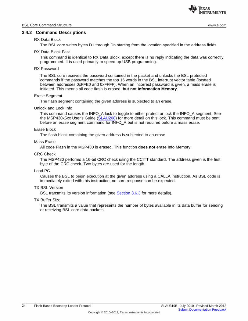
3.4.2 Command Descriptions
RX Data BlockThe BSL core writes bytes D1 through Dn starting from the location specified in the address fields.
RX Data Block FastThis command is identical to RX Data Block, except there is no reply indicating the data was correctlyprogrammed. It is used primarily to speed up USB programming.
RX Password
The BSL core receives the password contained in the packet and unlocks the BSL protectedcommands if the password matches the top 16 words in the BSL interrupt vector table (locatedbetween addresses 0xFFE0 and 0xFFFF). When an incorrect password is given, a mass erase isinitiated. This means all code flash is erased, but not Information Memory.
Erase SegmentThe flash segment containing the given address is subjected to an erase.
Unlock and Lock InfoThis command causes the INFO_A lock to toggle to either protect or lock the INFO_A segment. Seethe MSP430x5xx User's Guide (SLAU208) for more detail on this lock. This command must be sentbefore an erase segment command for INFO_A but is not required before a mass erase.
Erase BlockThe flash block containing the given address is subjected to an erase.
Mass EraseAll code Flash in the MSP430 is erased. This function does not erase Info Memory.
CRC CheckThe MSP430 performs a 16-bit CRC check using the CCITT standard. The address given is the firstbyte of the CRC check. Two bytes are used for the length.
Load PCCauses the BSL to begin execution at the given address using a CALLA instruction. As BSL code isimmediately exited with this instruction, no core response can be expected.
TX BSL VersionBSL transmits its version information (see Section 3.6.3 for more details).
TX Buffer SizeThe BSL transmits a value that represents the number of bytes available in its data buffer for sendingor receiving BSL core data packets.
24 Flash-Based Bootstrap Loader Protocol SLAU319B–July 2010–Revised March 2012Submit Documentation Feedback
Copyright © 2010–2012, Texas Instruments Incorporated
www.ti.com BSL Security
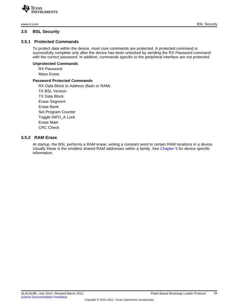
3.5 BSL Security
3.5.1 Protected Commands
To protect data within the device, most core commands are protected. A protected command issuccessfully complete only after the device has been unlocked by sending the RX Password commandwith the correct password. In addition, commands specific to the peripheral interface are not protected.
Unprotected CommandsRX PasswordMass Erase
Password Protected CommandsRX Data Block to Address (flash or RAM)TX BSL VersionTX Data BlockErase SegmentErase BankSet Program CounterToggle INFO_A LockErase MainCRC Check
3.5.2 RAM Erase
At startup, the BSL performs a RAM erase, writing a constant word to certain RAM locations in a device.Usually these is the smallest shared RAM addresses within a family. See Chapter 5 for device specificinformation.
25SLAU319B–July 2010–Revised March 2012 Flash-Based Bootstrap Loader ProtocolSubmit Documentation Feedback
Copyright © 2010–2012, Texas Instruments Incorporated
BSL Core Responses www.ti.com
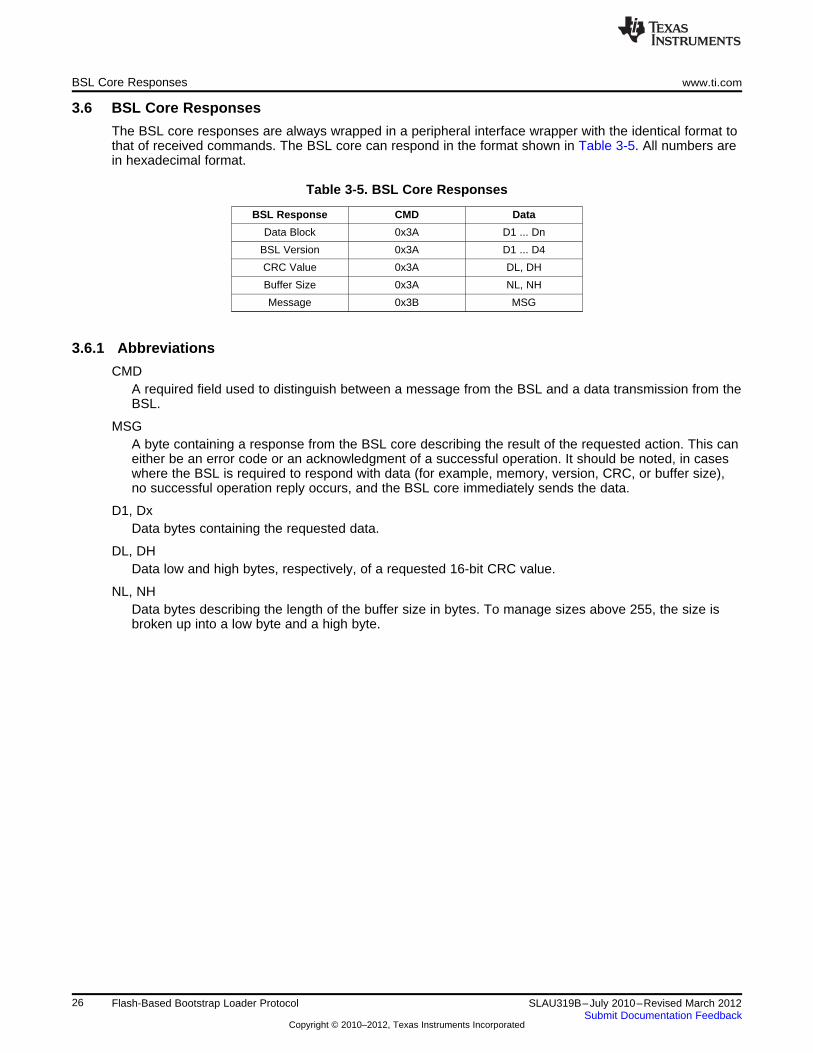
3.6 BSL Core Responses
The BSL core responses are always wrapped in a peripheral interface wrapper with the identical format tothat of received commands. The BSL core can respond in the format shown in Table 3-5. All numbers arein hexadecimal format.
Table 3-5. BSL Core Responses
BSL Response CMD Data
Data Block 0x3A D1 ... Dn
BSL Version 0x3A D1 ... D4
CRC Value 0x3A DL, DH
Buffer Size 0x3A NL, NH
Message 0x3B MSG
3.6.1 Abbreviations
CMDA required field used to distinguish between a message from the BSL and a data transmission from theBSL.
MSGA byte containing a response from the BSL core describing the result of the requested action. This caneither be an error code or an acknowledgment of a successful operation. It should be noted, in caseswhere the BSL is required to respond with data (for example, memory, version, CRC, or buffer size),no successful operation reply occurs, and the BSL core immediately sends the data.
D1, DxData bytes containing the requested data.
DL, DHData low and high bytes, respectively, of a requested 16-bit CRC value.
NL, NHData bytes describing the length of the buffer size in bytes. To manage sizes above 255, the size isbroken up into a low byte and a high byte.
26 Flash-Based Bootstrap Loader Protocol SLAU319B–July 2010–Revised March 2012Submit Documentation Feedback
Copyright © 2010–2012, Texas Instruments Incorporated

www.ti.com BSL Core Responses
3.6.2 BSL Core Messages
Table 3-6 describes the BSL core messages.
Table 3-6. BSL Core Messages
MSG Meaning
0x00 Operation Successful
Flash Write Check Failed. After programming, a CRC is run on the programmed data. If the CRC does not match0x01 the expected result, this error is returned.
Flash Fail Bit Set. An operation set the FAIL bit in the flash controller (see the MSP430x5xx User's Guide0x02 (SLAU208) for more details on the flash fail bit).
Voltage Change During Program. The VPE was set during the requested write operation (see the MSP430x5xx0x03 User's Guide (SLAU208) for more details on the VPE bit).
0x04 BSL Locked. The correct password has not yet been supplied to unlock the BSL.
0x05 BSL Password Error. An incorrect password was supplied to the BSL when attempting an unlock.
0x06 Byte Write Forbidden. This error is returned when a byte write is attempted in a flash area.
0x07 Unknown Command. The command given to the BSL was not recognized.
Packet Length Exceeds Buffer Size. The supplied packet length value is too large to be held in the BSL receive0x08 buffer.
3.6.3 BSL Version Number
The BSL version number is a 4-byte array.
Byte1: BSL Vendor informationTI BSL is always 0x00. Non-TI BSLs may use this area in another manner.
Byte 2: Command Interpreter VersionThe version number for the section of code that interprets BSL core commands.
Byte 3: API VersionThe version number for the section of code that reads and writes to MSP430 memory.Reserved bits:
0x80 Indicates this BSL can only execute the following commands:RX Data Block Fast (and can only write to RAM)RX PasswordSet PC
0x30 Indicates this BSL API interfaces with FRAM:
Byte 4: Peripheral Interface VersionThe version number for the section of code that manages communication.Reserved numbers:
0x00-0x2F: Indicates a Timer_A based UART0x20-0x4F: Indicates USB0x50-0x6F: Indicates USCI based UART0x70-0x8F: Indicates eUSCI based UART
27SLAU319B–July 2010–Revised March 2012 Flash-Based Bootstrap Loader ProtocolSubmit Documentation Feedback
Copyright © 2010–2012, Texas Instruments Incorporated
BSL Public Functions and Z-Area www.ti.com
3.6.4 Example Sequences for UART BSL
NOTE: All values in the example sequences are hexadecimal.
Changing baud rate to 9600Host: 80 02 00 52 02 90 55BSL: 00
Get buffer sizeHost: 80 01 00 1A 8B 52BSL: 00 80 03 00 3A 04 01 1D 12
Get BSL versionHost: 80 01 00 19 E8 62BSL: 00 80 05 00 3A 00 01 01 01 6C 4F
RX password to unlock BSLHost: 80 11 00 11 FF FF FF FF FF FF FF FF FF FF FF FF FF FF 00 5C 38 4FBSL: 00 80 02 00 3B 00 60 C4
3.7 BSL Public Functions and Z-Area
The BSL Z-Area is a small section of memory that can be read and invoked from Application code. It islocated at memory addresses 0x1000-0x100F.
Memory location 0x1000 contains a jump instruction pointing to the BSL start, it can be used to invoke theBSL from a running application.
Memory location 0x1002 contains a jump to the "BSL Action" function. To invoke the action function 3parameters are needed. The first parameter is a number describing which function, the second two aresimply known values indicating the function was called on purpose.
R12: The function numberR13: 0xDEADR14: 0xBEEF
3.7.1 Starting the BSL From an External Application
Setting the program counter to the memory location 0x1000 starts the BSL. The stack is always reset, andRAM is cleared. It should be noted that the GIE bit is not disabled, so this should be done by the callingapplication if interrupts are not desired and appropriately returned from "Return to BSL" if they are used.
Because the stack is reset, the location 0x1000 may also be called as a C function, as in the followingexample code:((void (*)())0x1000)();
3.7.2 Function Description
Function number: 2
Function Name: Return to BSL
Description: Any supplied function number calls the return to BSL function. This function can be used isthe BSL has written a program into Flash or RAM, started that program by "Set PC", and then the programneeds to return to the BSL. This function executes the following code:RETURN_TO_BSL
POP.W RET_low ; remove first word from return addrPOP.W RET_high ; remove second word from return addr
RETA ; should now return to the BSL location
28 Flash-Based Bootstrap Loader Protocol SLAU319B–July 2010–Revised March 2012Submit Documentation Feedback
Copyright © 2010–2012, Texas Instruments Incorporated
TL062D
TL062D
Chapter 4SLAU319B–July 2010–Revised March 2012
Bootstrap Loader Hardware
This chapter describes simple and low-cost hardware and software solutions to access the bootstraploader functions of the MSP430 flash devices through the serial port (RS-232) of a PC.
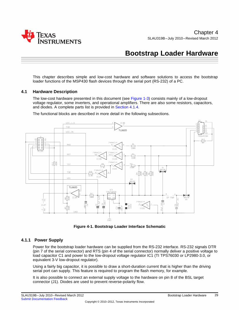
4.1 Hardware Description
The low-cost hardware presented in this document (see Figure 1-3) consists mainly of a low-dropoutvoltage regulator, some inverters, and operational amplifiers. There are also some resistors, capacitors,and diodes. A complete parts list is provided in Section 4.1.4.
The functional blocks are described in more detail in the following subsections.
Figure 4-1. Bootstrap Loader Interface Schematic
4.1.1 Power Supply
Power for the bootstrap loader hardware can be supplied from the RS-232 interface. RS-232 signals DTR(pin 7 of the serial connector) and RTS (pin 4 of the serial connector) normally deliver a positive voltage toload capacitor C1 and power to the low-dropout voltage regulator IC1 (TI TPS76030 or LP2980-3.0, orequivalent 3-V low-dropout regulator).
Using a fairly big capacitor, it is possible to draw a short-duration current that is higher than the drivingserial port can supply. This feature is required to program the flash memory, for example.
It is also possible to connect an external supply voltage to the hardware on pin 8 of the BSL targetconnector (J1). Diodes are used to prevent reverse-polarity flow.
29SLAU319B–July 2010–Revised March 2012 Bootstrap Loader HardwareSubmit Documentation Feedback
Copyright © 2010–2012, Texas Instruments Incorporated
Hardware Description www.ti.com
4.1.2 Serial Interface
Table 4-1 shows the signals used to communicate with the bootstrap loader (through connector J2). Thenames reflect the pin function as seen from the PC. For example, the PC receives data through the RxDpin, whereas the bootstrap loader needs to drive this signal.
Table 4-1. Serial-Port Signals and Pin Assignments
PIN NAME FULL NAME (PC) 9-PIN SUB-D FUNCTION ON BSL INTERFACE
RxD Receive data 2 Transmit data to PC
TxD Transmit data 3 Receive data from PC (and negative supply)
DTR Data terminal ready 4 Reset control (and positive supply)
RTS Request to send 7 TEST or TCK control (and positive supply)
GND Ground 5 Ground
4.1.2.1 Level Shifting
Simple CMOS inverters with Schmitt-trigger characteristics (IC2) are used to transform the RS-232 levels(see Table 4-2) to CMOS levels.
Table 4-2. RS-232 Levels
LOGIC LEVEL RS-232 LEVEL RS-232 VOLTAGE LEVEL
1 Mark –3 V to –15 V
0 Space 3 V to 15 V
The inverters are powered by the operational amplifier IC3A. This amplifier permits adjusting the providedlogic level to the requirements of the connected target application. A voltage applied to pin 8 of the BSLtarget connector (VCC_IN) overrides the default 3-V level provided from IC1 and the 100-kΩ seriesresistor R11. Thus, the output voltage of the operational amplifier is pulled to the applied voltage VCC_IN.
Depending on the overvoltage protection of the device family selected, the excess voltage is eitherconducted to VCC (as in the TI '74HC14) or to GND (as in the TI '74AHC14). If the protection diodeconducts to VCC, the operational amplifier IC3A needs to compensate for the overvoltage. Therefore, the'74AHC14 device, which conducts to ground (GND), is recommended.
To avoid excessive power dissipation and damage of the protection diodes, series resistors (R1, R2, andR3) are used to limit the input current.
An operational amplifier (IC3B) is used to generate RS-232 levels out of CMOS levels. The level at thepositive input is set to VCC/2 (1.5 V nominal). If the level at the negative input rises above this level, theoutput is pulled to the negative supply of the operational amplifier (mark). If the level drops below VCC/2,the output is pulled to the positive rail (space).
The positive supply of the operational amplifier is the same as the input to the voltage regulator. Aseparate capacitor (C5) is used to generate the negative-supply voltage. This capacitor is charged by thereceiving signal of the bootstrap loader hardware (pin 3 on SUB-D connector J2).
During an asynchronous serial communication, the combination of stop bit and start bit is used tosynchronize sender and receiver. After the transmission of a data byte, the stop bit forces the transmissionline into a defined state, which is usually a logic 1 or, in RS-232 terms, a mark. This means that thetransmission-line voltage is negative when there is no transmission and the capacitor can be charged.Diodes are used to prevent discharge of the capacitor during transmission.
In very rare circumstances, the data sent to the bootstrap loader interface might hold too many zeros, sothat the capacitor C5 required for the negative supply is discharged, causing a malfunction of theinterface. (A possible workaround is to send the data in smaller chunks.) But under normal operatingconditions, even data containing all zeros does not cause problems.
30 Bootstrap Loader Hardware SLAU319B–July 2010–Revised March 2012Submit Documentation Feedback
Copyright © 2010–2012, Texas Instruments Incorporated
www.ti.com Hardware Description
4.1.2.2 Control of RST/NMI and TEST or TCK Pins
The two pins used to invoke the bootstrap loader software of the MSP430—RST/NMI and TEST or TCK(for devices without a dedicated TEST pin)—are controlled by the DTR and RTS signals, respectively.These signals also deliver a positive voltage to supply the bootstrap loader hardware.
For devices with a dedicated TEST pin, the levels at RST/NMI and TEST during normal operation arelogic 1 and logic 0, respectively. To achieve these levels and to use the corresponding RS-232 signals aspower-supply lines, it is necessary to use two inverters (IC1A, IC2B) for the RST/NMI pin and one inverter(IC2E) for the TEST pin.
Devices without the TEST pin require the inverted TEST pin sequence on their TCK pin to invoke thebootstrap loader. Thus, the corresponding signal is inverted (inverter IC2F).
Diodes prevent discharge of capacitor C1 to allow control of the RS-232 lines (RTS and DTR).
4.1.3 Target Connector
Table 4-3. Pin Assignment of Target Connector (1)
PIN ON MSP430F13x ORPIN SIGNAL NAME DEVICES WITH TEST PIN PIN ON MSP430F4xxMSP430F14x
1 TXD P1.1 P1.1 P1.0
2 TCK Do not connect (2) TCK TCK
3 RXD P2.2 P2.2 P1.1
4 RST RST/NMI RST/NMI RST/NMI
5 GND GND GND GND
6 VCC (3.0 V) VCC(3) VCC
(3) VCC(3)
7 TST TEST Do not connect Do not connect
8 VCC_IN VCC(3) VCC
(3) VCC(3)
9 Not connected — — —
10 Not connected — — —(1) For device-specific BSL pin information, see the applicable device data sheet.(2) Signal TCK must not be connected on devices with the TEST pin.(3) Pin VCC (3.0 V) is a voltage source that can provide a limited current, depending on the serial port driver capability. If an external
power supply is used, VCC (3.0 V) must not be connected to the target. In this case, the external supply voltage must beconnected to pin VCC_IN. Otherwise, VCC_IN must be unconnected.
31SLAU319B–July 2010–Revised March 2012 Bootstrap Loader HardwareSubmit Documentation Feedback
Copyright © 2010–2012, Texas Instruments Incorporated

Hardware Description www.ti.com
4.1.4 Parts List
Table 4-4. Universal BSL Interface Parts List
VALUE ORPART PACKAGE COMMENTPART NUMBER
C1 33 µF, 16 V SMD 7243
C2 100 nF SMD 0805
C3 2.2 µF, 6.3 V SMD 1206
C4 100 nF SMD 0805
C5 33 µF, 16 V SMD 7243
C6 100 nF SMD 0805
D1 BAV70 SOT23 High-speed double diode
D2 BAV70 SOT23 High-speed double diode
D3 BAV70 SOT23
IC1 TPS76030 SOT23-5 TI
IC2 74AHC14 SO14 TI
IC3 TL062D SO8 TI
R1 330 kΩ SMD 0805
R2 330 kΩ SMD 0805
R3 330 kΩ SMD 0805
R4 680 kΩ SMD 0805
R5 680 kΩ SMD 0805
R6 680 kΩ SMD 0805
R7 330 kΩ SMD 0805
R8 330 kΩ SMD 0805
R9 3.3 kΩ SMD 0805
R10 3.3 kΩ SMD 0805
R11 100 kΩ SMD 0805
R12 0 kΩ SMD 0805
R13 680 kΩ SMD 0805
J1 Header 2x5 2X05 Target connector (see Table 4-3)
J2 F09HP284 9-SUB-D female RS-232 connector
CON3 RESET SMD0805 Pads to connect an optional reset button
32 Bootstrap Loader Hardware SLAU319B–July 2010–Revised March 2012Submit Documentation Feedback
Copyright © 2010–2012, Texas Instruments Incorporated

Chapter 5SLAU319B–July 2010–Revised March 2012
Differences Between Devices and Bootstrap LoaderVersions
5.1 5xx and 6xx BSL Versions
BSL Version 00.01.01.01
Devices MSP430F543x family
RAM erased none
Buffer size for Core 260 bytesCommands
Notable Information 1. The BSL does not contain a mechanism to unlock the BSL area for erasing and writing a custom BSL.This function is not supported in this version. The BSL may be safely erased however.
2. The only supported baud rates are 9600 and 57600.3. The BSL transmits on TA0.0 and receives on TA0.1.4. The BSL does not expect a parity bit.
Known Bugs 1. The password for the BSL is the bytes between addresses 0xFFF0 and 0xFFFF. This means that thisBSL version expects only 16 bytes for a password in the RX Password command. Sending 32 bytesreturns an error.
2. If the addresses 0x20396 or 0x20397 are included in the address range of the CRC command, thereturned data is incorrect.
3. The Mass Erase command also erases Info_A.4. On incorrect password, the device erases all RAM, including its stack. Thus, proper returning of an error
code is not assured.5. The total number of bytes for the CRC function is masked with 0x7FFF and is, therefore, limited to
32767.
BSL Version 00.05.04.03
Devices MSP430F543xA family
RAM erased 0x1C00–0x5BFF
Buffer size for Core 260 bytesCommands
Notable Information 1. The BSL transmits on TA0.0 and receives on TA0.1.
Known Bugs 1. The baud rate of 115k cannot be ensured across all clock, voltage, and temperature variations.2. To invoke this BSL using the TEST/RESET method, the second low pulse on TEST must be shorter
than 15 µs.
BSL Version 00.05.04.52
Devices CC430F613x family
RAM erased 0x1C00–0x23FF
Buffer size for Core 260 bytesCommands
Notable Information 1. The BSL transmits on UCA0TXD and receives on UCA0RXD.
Known Bugs 1. The baud rate 115k can not be ensured across all clock, voltage, and temperature variations.
33SLAU319B–July 2010–Revised March 2012 Differences Between Devices and Bootstrap Loader VersionsSubmit Documentation Feedback
Copyright © 2010–2012, Texas Instruments Incorporated

Special Consideration for ROM BSL Version 1.10 www.ti.com
BSL Version 00.03.83.33
Devices MSP430F552x family
RAM erased 0x2400–0x33FF
MAX_BUFFER_SIZE 62 bytes
Notable Information 1. BSL in device is RAM write only. Full BSL must first be loaded into device RAM and started to performflash write. Only the commands RX PASSWORD, RX DATA BLOCK FAST, and SET PC aresupported.
Known Bugs
BSL Version 00.04.31.71
Devices MSP430FR573x family
RAM erased 0x1C00–0x1FFF
Buffer size for Core 260 bytesCommands
Notable Information 1. The BSL transmits on UCA0TXD and receives on UCA0RXD.2. If the BSL is started with MPULOCK bit set, the BSL is unable to clear it, and mass erases could be
incomplete.
Known Bugs
5.2 Special Consideration for ROM BSL Version 1.10
The first official version V1.10 of the ROM BSL requires a small loadable patch sequence, PATCH.TXT, toreliably execute the RX block command. The same procedure must be executed if a loadable BSL isdownloaded to such a device. After the BSL has been started, proceed in the following manner:
• RX password (unlock password protection for the following command)
• Load program counter (PC) with 0C22h (initialize stack pointer to a safe address)
• RX password again (unlock password protection for subsequent commands)
• RX data block (code of loadable patch, code section address is 0220h)
• TX data block (code of loadable patch for verification)
From this time forward, the RX block and TX block commands can be used with one restriction: prior totheir invocation, the program counter must be set to the start address of the patch.
• Load program counter (PC) with start address 0220h of loadable patch
• RX data block (code to be programmed at any location), or
• TX data block (from any location)
5.3 ROM BSL Known Issues
BSL Command Erase Main or Info
Versions Affected 1.x
Description Does not erase information memory when supplied with address in info memory
Workarounds Use Erase Segment Command
BSL Command Erase Main or Info
Versions Affected 1.x
Reports failure when first segment of code memory is supplied as address. Erase is properly performedDescription however
Workarounds Use any other main memory address
34 Differences Between Devices and Bootstrap Loader Versions SLAU319B–July 2010–Revised March 2012Submit Documentation Feedback
Copyright © 2010–2012, Texas Instruments Incorporated
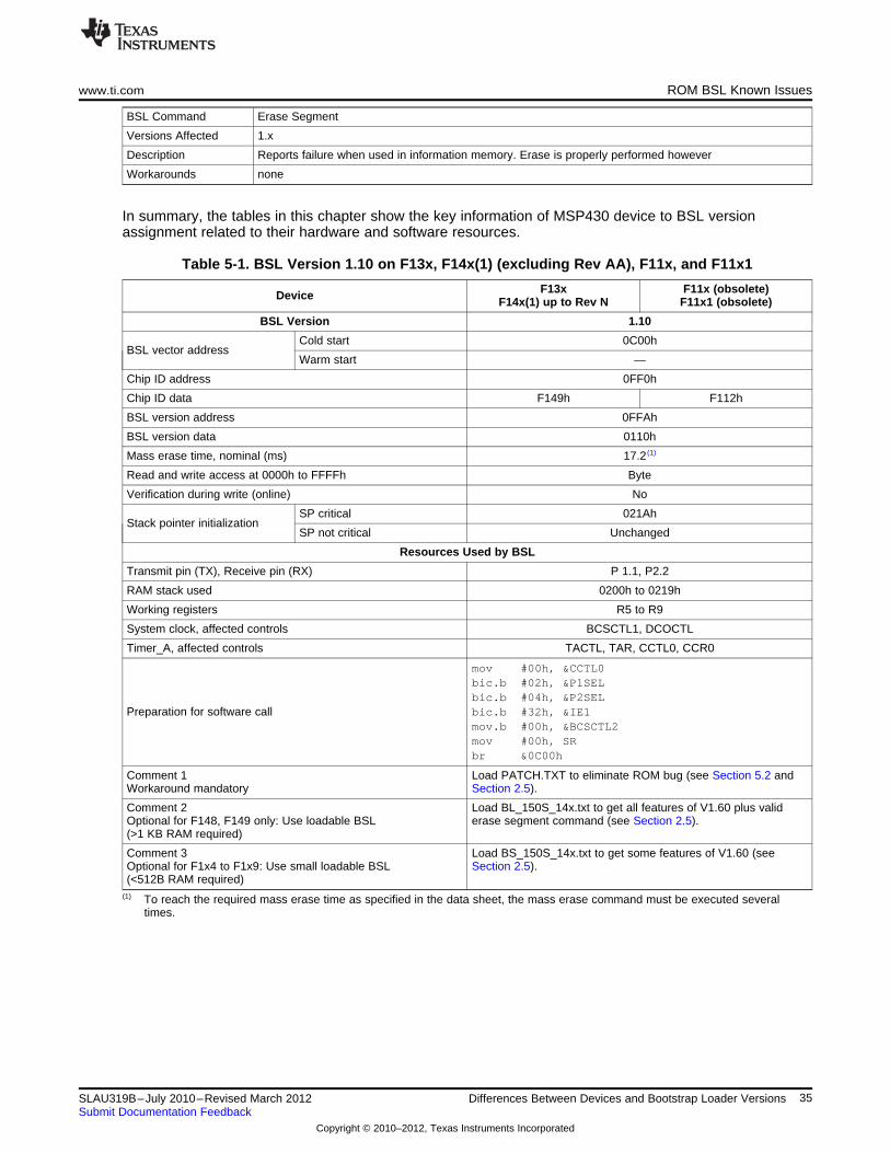
www.ti.com ROM BSL Known Issues
BSL Command Erase Segment
Versions Affected 1.x
Description Reports failure when used in information memory. Erase is properly performed however
Workarounds none
In summary, the tables in this chapter show the key information of MSP430 device to BSL versionassignment related to their hardware and software resources.
Table 5-1. BSL Version 1.10 on F13x, F14x(1) (excluding Rev AA), F11x, and F11x1
F13x F11x (obsolete)Device F14x(1) up to Rev N F11x1 (obsolete)
BSL Version 1.10
Cold start 0C00hBSL vector address
Warm start —
Chip ID address 0FF0h
Chip ID data F149h F112h
BSL version address 0FFAh
BSL version data 0110h
Mass erase time, nominal (ms) 17.2 (1)
Read and write access at 0000h to FFFFh Byte
Verification during write (online) No
SP critical 021AhStack pointer initialization
SP not critical Unchanged
Resources Used by BSL
Transmit pin (TX), Receive pin (RX) P 1.1, P2.2
RAM stack used 0200h to 0219h
Working registers R5 to R9
System clock, affected controls BCSCTL1, DCOCTL
Timer_A, affected controls TACTL, TAR, CCTL0, CCR0
mov #00h, &CCTL0bic.b #02h, &P1SELbic.b #04h, &P2SEL
Preparation for software call bic.b #32h, &IE1mov.b #00h, &BCSCTL2mov #00h, SRbr &0C00h
Comment 1 Load PATCH.TXT to eliminate ROM bug (see Section 5.2 andWorkaround mandatory Section 2.5).
Comment 2 Load BL_150S_14x.txt to get all features of V1.60 plus validOptional for F148, F149 only: Use loadable BSL erase segment command (see Section 2.5).(>1 KB RAM required)
Comment 3 Load BS_150S_14x.txt to get some features of V1.60 (seeOptional for F1x4 to F1x9: Use small loadable BSL Section 2.5).(<512B RAM required)
(1) To reach the required mass erase time as specified in the data sheet, the mass erase command must be executed severaltimes.
35SLAU319B–July 2010–Revised March 2012 Differences Between Devices and Bootstrap Loader VersionsSubmit Documentation Feedback
Copyright © 2010–2012, Texas Instruments Incorporated
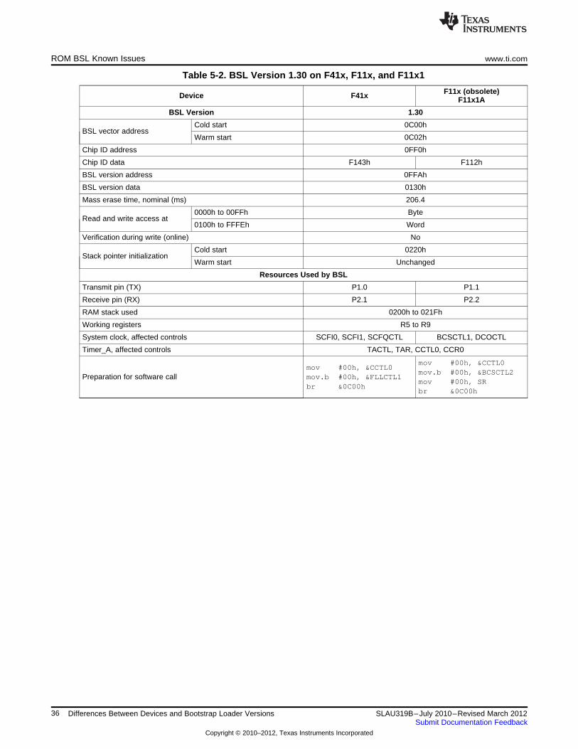
ROM BSL Known Issues www.ti.com
Table 5-2. BSL Version 1.30 on F41x, F11x, and F11x1
F11x (obsolete)Device F41x F11x1A
BSL Version 1.30
Cold start 0C00hBSL vector address
Warm start 0C02h
Chip ID address 0FF0h
Chip ID data F143h F112h
BSL version address 0FFAh
BSL version data 0130h
Mass erase time, nominal (ms) 206.4
0000h to 00FFh ByteRead and write access at
0100h to FFFEh Word
Verification during write (online) No
Cold start 0220hStack pointer initialization
Warm start Unchanged
Resources Used by BSL
Transmit pin (TX) P1.0 P1.1
Receive pin (RX) P2.1 P2.2
RAM stack used 0200h to 021Fh
Working registers R5 to R9
System clock, affected controls SCFI0, SCFI1, SCFQCTL BCSCTL1, DCOCTL
Timer_A, affected controls TACTL, TAR, CCTL0, CCR0
mov #00h, &CCTL0mov #00h, &CCTL0
mov.b #00h, &BCSCTL2Preparation for software call mov.b #00h, &FLLCTL1
mov #00h, SRbr &0C00h
br &0C00h
36 Differences Between Devices and Bootstrap Loader Versions SLAU319B–July 2010–Revised March 2012Submit Documentation Feedback
Copyright © 2010–2012, Texas Instruments Incorporated
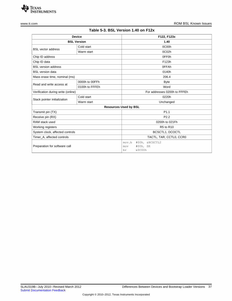
www.ti.com ROM BSL Known Issues
Table 5-3. BSL Version 1.40 on F12x
Device F122, F123x
BSL Version 1.40
Cold start 0C00hBSL vector address
Warm start 0C02h
Chip ID address 0FF0h
Chip ID data F123h
BSL version address 0FFAh
BSL version data 0140h
Mass erase time, nominal (ms) 206.4
0000h to 00FFh ByteRead and write access at
0100h to FFFEh Word
Verification during write (online) For addresses 0200h to FFFEh
Cold start 0220hStack pointer initialization
Warm start Unchanged
Resources Used by BSL
Transmit pin (TX) P1.1
Receive pin (RX) P2.2
RAM stack used 0200h to 021Fh
Working registers R5 to R10
System clock, affected controls BCSCTL1, DCOCTL
Timer_A, affected controls TACTL, TAR, CCTL0, CCR0
mov.b #00h, &BCSCTL2Preparation for software call mov #00h, SR
br &0C00h
37SLAU319B–July 2010–Revised March 2012 Differences Between Devices and Bootstrap Loader VersionsSubmit Documentation Feedback
Copyright © 2010–2012, Texas Instruments Incorporated

ROM BSL Known Issues www.ti.com
Table 5-4. BSL Version 1.60 on F11x2, F12x2, F43x, F44x, FE42x, FW42x, F(G)43x, F415, F417
FE42x,F1122, F1222, F43x, FW42x,Device F(G)43xF1132 F1232 F44x F415,
F417
BSL Version 1.60
Cold start 0C00hBSL vector address
Warm start 0C02h
Chip ID address 0FF0h
Chip ID data 1132h 1232h F449h F427h F439h
BSL version address 0FFAh
BSL version data 0160h
Mass erase time, nominal (ms) 206.4
0000h to 00FFh ByteRead and writeaccess at 0100h to FFFEh Word
Verification during write (online) For addresses 0200h to FFFEh
Erase check command Yes (error address 0200h)
Erase segment command With erasure verification (error address 0200h)
TX identification command Yes
Change baud rate command Yes
Cold start 0220hStack pointerinitialization Warm start Unchanged
Resources Used by BSL
Transmit pin (TX) P1.1 P1.0
Receive pin (RX) P2.2 P1.1
RAM stack used 0200h to 021Fh
Working registers R5 to R12
System clock, affected controls BCSCTL1, DCOCTL SCFI0, SCFI1, SCFQCTL
Timer_A, affected controls TACTL, TAR, CCTL0, CCR0
mov.b #00h, &BCSCTL2 mov.b #00h, &FLLCTL1Preparation for software call mov #00h, SR br &0C00h
br &0C00h
Erase segment Addresses 1000h to 11FFh are verified coherently (three segments). Also use eraseComment command check command.
38 Differences Between Devices and Bootstrap Loader Versions SLAU319B–July 2010–Revised March 2012Submit Documentation Feedback
Copyright © 2010–2012, Texas Instruments Incorporated
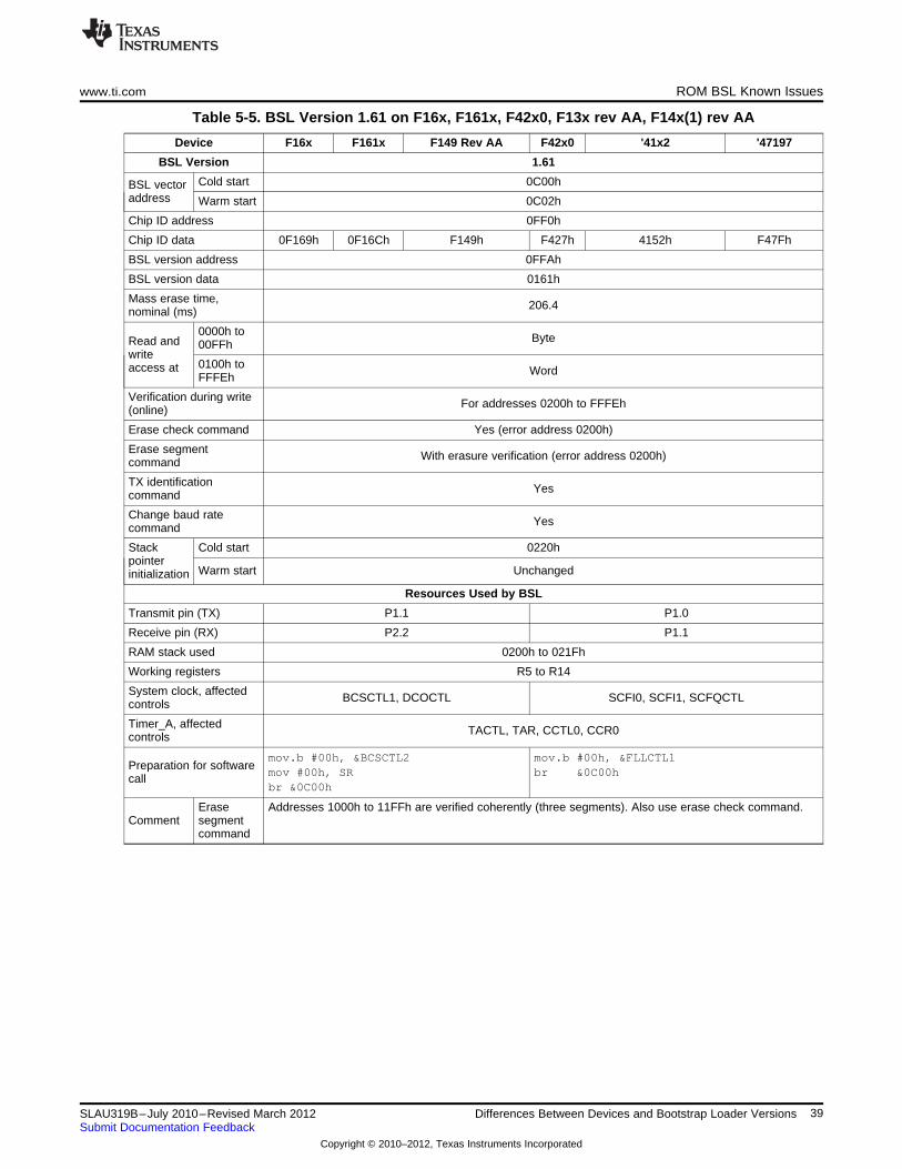
www.ti.com ROM BSL Known Issues
Table 5-5. BSL Version 1.61 on F16x, F161x, F42x0, F13x rev AA, F14x(1) rev AA
Device F16x F161x F149 Rev AA F42x0 '41x2 '47197
BSL Version 1.61
Cold start 0C00hBSL vectoraddress Warm start 0C02h
Chip ID address 0FF0h
Chip ID data 0F169h 0F16Ch F149h F427h 4152h F47Fh
BSL version address 0FFAh
BSL version data 0161h
Mass erase time, 206.4nominal (ms)
0000h to ByteRead and 00FFhwrite
0100h toaccess at WordFFFEh
Verification during write For addresses 0200h to FFFEh(online)
Erase check command Yes (error address 0200h)
Erase segment With erasure verification (error address 0200h)command
TX identification Yescommand
Change baud rate Yescommand
Stack Cold start 0220hpointer
Warm start Unchangedinitialization
Resources Used by BSL
Transmit pin (TX) P1.1 P1.0
Receive pin (RX) P2.2 P1.1
RAM stack used 0200h to 021Fh
Working registers R5 to R14
System clock, affected BCSCTL1, DCOCTL SCFI0, SCFI1, SCFQCTLcontrols
Timer_A, affected TACTL, TAR, CCTL0, CCR0controls
mov.b #00h, &BCSCTL2 mov.b #00h, &FLLCTL1Preparation for software
mov #00h, SR br &0C00hcallbr &0C00h
Erase Addresses 1000h to 11FFh are verified coherently (three segments). Also use erase check command.Comment segment
command
39SLAU319B–July 2010–Revised March 2012 Differences Between Devices and Bootstrap Loader VersionsSubmit Documentation Feedback
Copyright © 2010–2012, Texas Instruments Incorporated
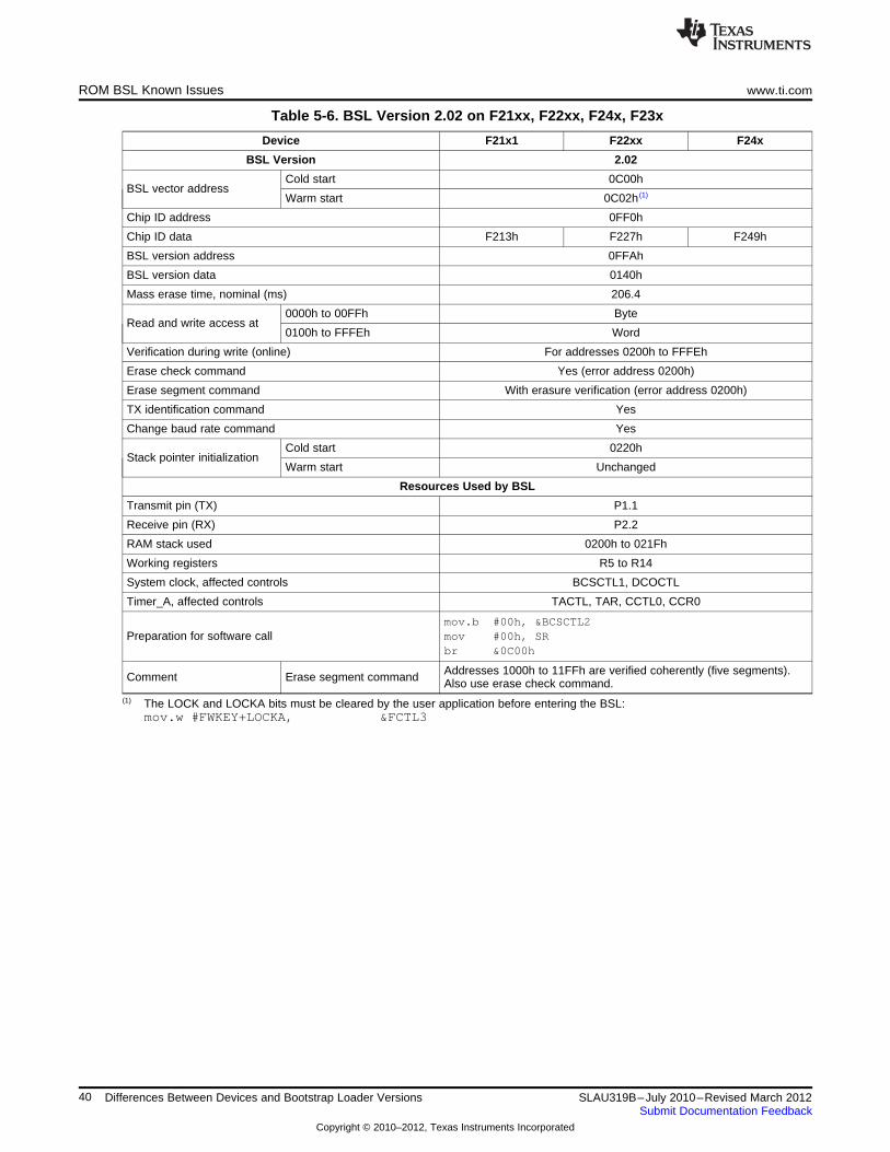
ROM BSL Known Issues www.ti.com
Table 5-6. BSL Version 2.02 on F21xx, F22xx, F24x, F23x
Device F21x1 F22xx F24x
BSL Version 2.02
Cold start 0C00hBSL vector address
Warm start 0C02h (1)
Chip ID address 0FF0h
Chip ID data F213h F227h F249h
BSL version address 0FFAh
BSL version data 0140h
Mass erase time, nominal (ms) 206.4
0000h to 00FFh ByteRead and write access at
0100h to FFFEh Word
Verification during write (online) For addresses 0200h to FFFEh
Erase check command Yes (error address 0200h)
Erase segment command With erasure verification (error address 0200h)
TX identification command Yes
Change baud rate command Yes
Cold start 0220hStack pointer initialization
Warm start Unchanged
Resources Used by BSL
Transmit pin (TX) P1.1
Receive pin (RX) P2.2
RAM stack used 0200h to 021Fh
Working registers R5 to R14
System clock, affected controls BCSCTL1, DCOCTL
Timer_A, affected controls TACTL, TAR, CCTL0, CCR0
mov.b #00h, &BCSCTL2Preparation for software call mov #00h, SR
br &0C00h
Addresses 1000h to 11FFh are verified coherently (five segments).Comment Erase segment command Also use erase check command.(1) The LOCK and LOCKA bits must be cleared by the user application before entering the BSL:
mov.w #FWKEY+LOCKA, &FCTL3
40 Differences Between Devices and Bootstrap Loader Versions SLAU319B–July 2010–Revised March 2012Submit Documentation Feedback
Copyright © 2010–2012, Texas Instruments Incorporated
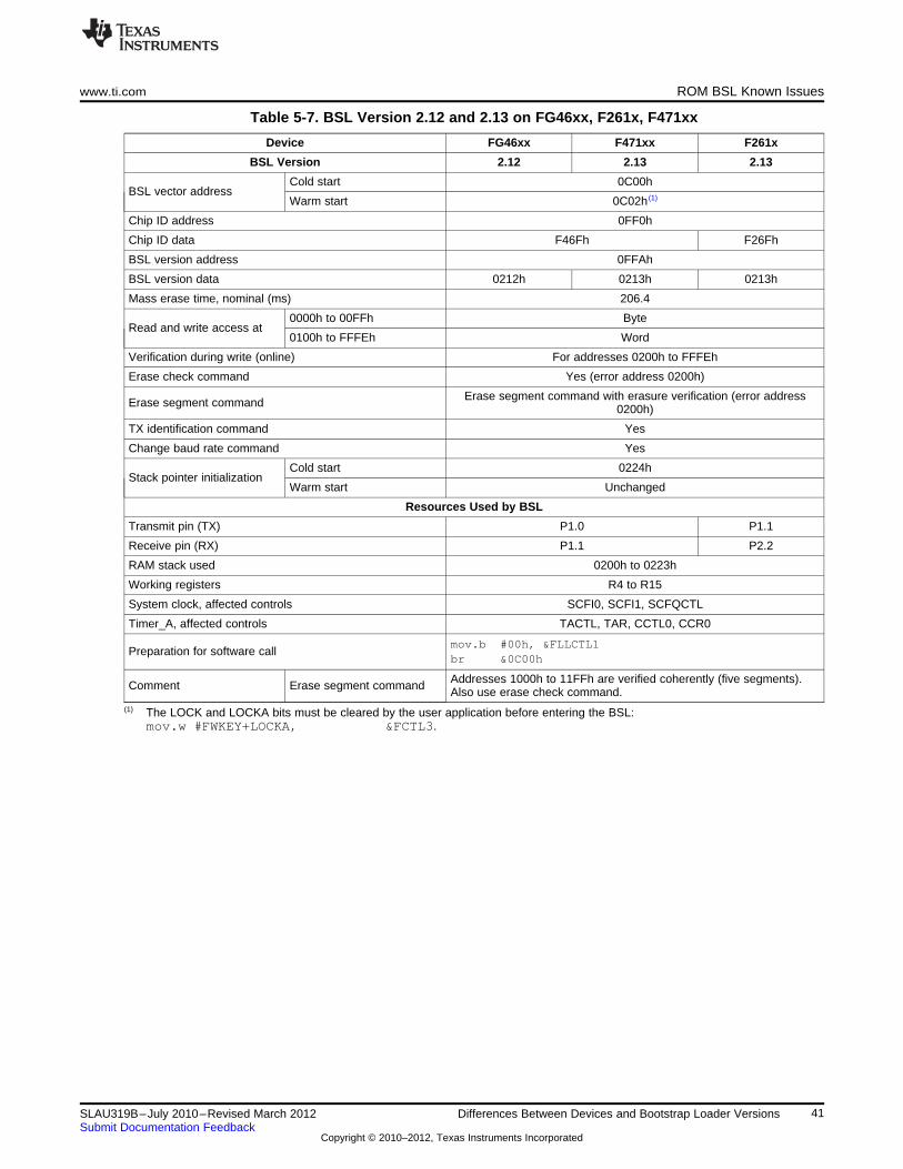
www.ti.com ROM BSL Known Issues
Table 5-7. BSL Version 2.12 and 2.13 on FG46xx, F261x, F471xx
Device FG46xx F471xx F261x
BSL Version 2.12 2.13 2.13
Cold start 0C00hBSL vector address
Warm start 0C02h (1)
Chip ID address 0FF0h
Chip ID data F46Fh F26Fh
BSL version address 0FFAh
BSL version data 0212h 0213h 0213h
Mass erase time, nominal (ms) 206.4
0000h to 00FFh ByteRead and write access at
0100h to FFFEh Word
Verification during write (online) For addresses 0200h to FFFEh
Erase check command Yes (error address 0200h)
Erase segment command with erasure verification (error addressErase segment command 0200h)
TX identification command Yes
Change baud rate command Yes
Cold start 0224hStack pointer initialization
Warm start Unchanged
Resources Used by BSL
Transmit pin (TX) P1.0 P1.1
Receive pin (RX) P1.1 P2.2
RAM stack used 0200h to 0223h
Working registers R4 to R15
System clock, affected controls SCFI0, SCFI1, SCFQCTL
Timer_A, affected controls TACTL, TAR, CCTL0, CCR0
mov.b #00h, &FLLCTL1Preparation for software call
br &0C00h
Addresses 1000h to 11FFh are verified coherently (five segments).Comment Erase segment command Also use erase check command.(1) The LOCK and LOCKA bits must be cleared by the user application before entering the BSL:
mov.w #FWKEY+LOCKA, &FCTL3.
41SLAU319B–July 2010–Revised March 2012 Differences Between Devices and Bootstrap Loader VersionsSubmit Documentation Feedback
Copyright © 2010–2012, Texas Instruments Incorporated

Special Note on the MSP430F14x Device Family BSL www.ti.com
5.4 Special Note on the MSP430F14x Device Family BSL
Revision AA of the MSP430F14x devices have a BSL that was updated to Version 1.61. The primaryreasons for this change were to increase IP security, ensure correct flash programming and mass erase,and to negate the need for using any patches during programming. To ensure a smooth transition, aprogramming environment should be updated to take into account the following changes:
• The Mass Erase command needs to be issued only once, and execution of this command takeslonger.
• Only word writes are allowed to flash memory.
• No patch or RAM loadable BSL is required.
• BSL has "online verification" to speed programming.
• Memory allocation has changed (see BSL version charts in Section 5.3).
• BSL can return a NAK if Segment Erase fails.
• Transmit BSL Version and Change Baud rate are now unprotected.
42 Differences Between Devices and Bootstrap Loader Versions SLAU319B–July 2010–Revised March 2012Submit Documentation Feedback
Copyright © 2010–2012, Texas Instruments Incorporated
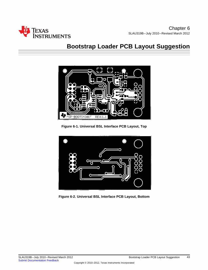
unitop.wmf@
unibottom.wmf@
Chapter 6SLAU319B–July 2010–Revised March 2012
Bootstrap Loader PCB Layout Suggestion
Figure 6-1. Universal BSL Interface PCB Layout, Top
Figure 6-2. Universal BSL Interface PCB Layout, Bottom
43SLAU319B–July 2010–Revised March 2012 Bootstrap Loader PCB Layout SuggestionSubmit Documentation Feedback
Copyright © 2010–2012, Texas Instruments Incorporated
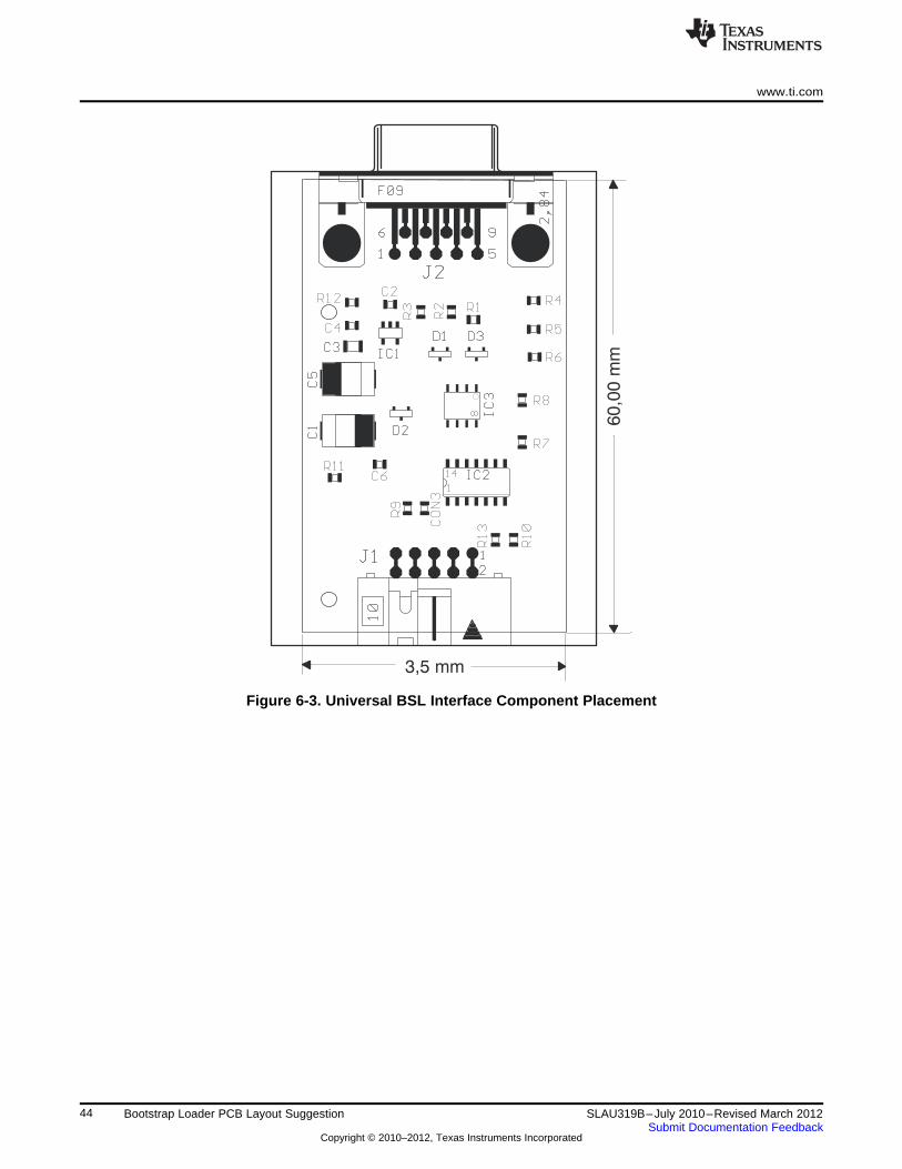
3,5 mm
60,0
0m
m
www.ti.com
Figure 6-3. Universal BSL Interface Component Placement
44 Bootstrap Loader PCB Layout Suggestion SLAU319B–July 2010–Revised March 2012Submit Documentation Feedback
Copyright © 2010–2012, Texas Instruments Incorporated
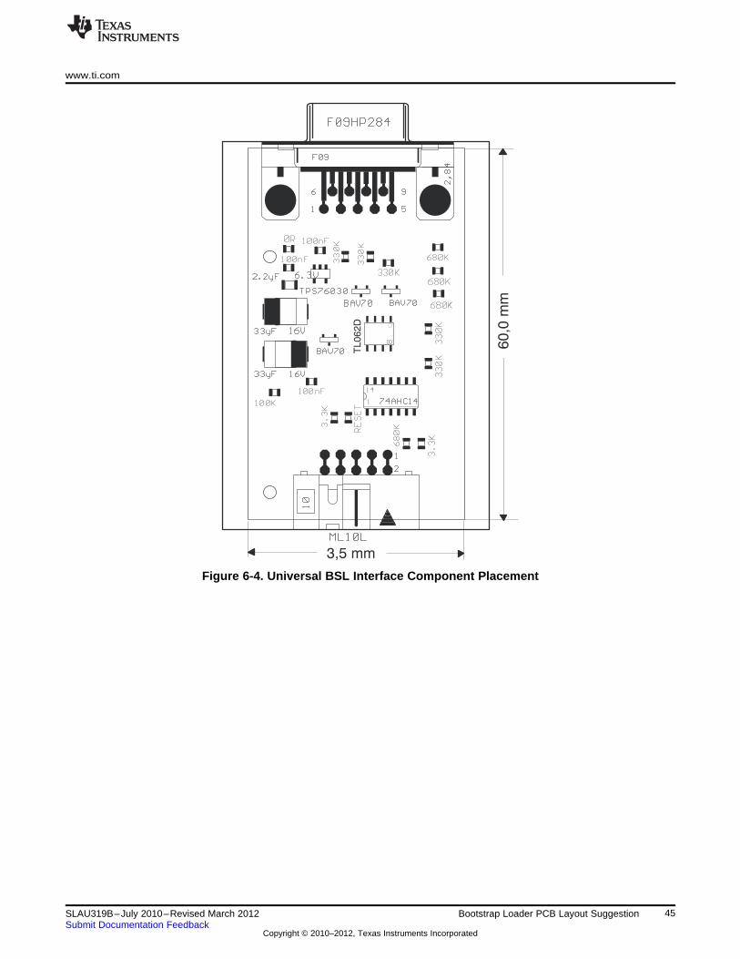
3,5 mm
60,0
mm
TL062D
www.ti.com
Figure 6-4. Universal BSL Interface Component Placement
45SLAU319B–July 2010–Revised March 2012 Bootstrap Loader PCB Layout SuggestionSubmit Documentation Feedback
Copyright © 2010–2012, Texas Instruments Incorporated
Revision History www.ti.com
Revision History
Changes from A Revision (August 2010) to B Revision ................................................................................................ Page
• Changed note regarding recommended minimum time for pin states ............................................................. 6• Changed note regarding recommended minimum time for pin states ............................................................. 7• Changed second "TO BSL" value .................................................................................................... 12
NOTE: Page numbers for previous revisions may differ from page numbers in the current version.
46 Revision History SLAU319B–July 2010–Revised March 2012Submit Documentation Feedback
Copyright © 2010–2012, Texas Instruments Incorporated
IMPORTANT NOTICE
Texas Instruments Incorporated and its subsidiaries (TI) reserve the right to make corrections, modifications, enhancements, improvements,and other changes to its products and services at any time and to discontinue any product or service without notice. Customers shouldobtain the latest relevant information before placing orders and should verify that such information is current and complete. All products aresold subject to TI’s terms and conditions of sale supplied at the time of order acknowledgment.
TI warrants performance of its hardware products to the specifications applicable at the time of sale in accordance with TI’s standardwarranty. Testing and other quality control techniques are used to the extent TI deems necessary to support this warranty. Except wheremandated by government requirements, testing of all parameters of each product is not necessarily performed.
TI assumes no liability for applications assistance or customer product design. Customers are responsible for their products andapplications using TI components. To minimize the risks associated with customer products and applications, customers should provideadequate design and operating safeguards.
TI does not warrant or represent that any license, either express or implied, is granted under any TI patent right, copyright, mask work right,or other TI intellectual property right relating to any combination, machine, or process in which TI products or services are used. Informationpublished by TI regarding third-party products or services does not constitute a license from TI to use such products or services or awarranty or endorsement thereof. Use of such information may require a license from a third party under the patents or other intellectualproperty of the third party, or a license from TI under the patents or other intellectual property of TI.
Reproduction of TI information in TI data books or data sheets is permissible only if reproduction is without alteration and is accompaniedby all associated warranties, conditions, limitations, and notices. Reproduction of this information with alteration is an unfair and deceptivebusiness practice. TI is not responsible or liable for such altered documentation. Information of third parties may be subject to additionalrestrictions.
Resale of TI products or services with statements different from or beyond the parameters stated by TI for that product or service voids allexpress and any implied warranties for the associated TI product or service and is an unfair and deceptive business practice. TI is notresponsible or liable for any such statements.
TI products are not authorized for use in safety-critical applications (such as life support) where a failure of the TI product would reasonablybe expected to cause severe personal injury or death, unless officers of the parties have executed an agreement specifically governingsuch use. Buyers represent that they have all necessary expertise in the safety and regulatory ramifications of their applications, andacknowledge and agree that they are solely responsible for all legal, regulatory and safety-related requirements concerning their productsand any use of TI products in such safety-critical applications, notwithstanding any applications-related information or support that may beprovided by TI. Further, Buyers must fully indemnify TI and its representatives against any damages arising out of the use of TI products insuch safety-critical applications.
TI products are neither designed nor intended for use in military/aerospace applications or environments unless the TI products arespecifically designated by TI as military-grade or "enhanced plastic." Only products designated by TI as military-grade meet militaryspecifications. Buyers acknowledge and agree that any such use of TI products which TI has not designated as military-grade is solely atthe Buyer's risk, and that they are solely responsible for compliance with all legal and regulatory requirements in connection with such use.
TI products are neither designed nor intended for use in automotive applications or environments unless the specific TI products aredesignated by TI as compliant with ISO/TS 16949 requirements. Buyers acknowledge and agree that, if they use any non-designatedproducts in automotive applications, TI will not be responsible for any failure to meet such requirements.
Following are URLs where you can obtain information on other Texas Instruments products and application solutions:
Products Applications
Audio www.ti.com/audio Automotive and Transportation www.ti.com/automotive
Amplifiers amplifier.ti.com Communications and Telecom www.ti.com/communications
Data Converters dataconverter.ti.com Computers and Peripherals www.ti.com/computers
DLP® Products www.dlp.com Consumer Electronics www.ti.com/consumer-apps
DSP dsp.ti.com Energy and Lighting www.ti.com/energy
Clocks and Timers www.ti.com/clocks Industrial www.ti.com/industrial
Interface interface.ti.com Medical www.ti.com/medical
Logic logic.ti.com Security www.ti.com/security
Power Mgmt power.ti.com Space, Avionics and Defense www.ti.com/space-avionics-defense
Microcontrollers microcontroller.ti.com Video and Imaging www.ti.com/video
RFID www.ti-rfid.com
OMAP Mobile Processors www.ti.com/omap
Wireless Connectivity www.ti.com/wirelessconnectivity
TI E2E Community Home Page e2e.ti.com
Mailing Address: Texas Instruments, Post Office Box 655303, Dallas, Texas 75265Copyright © 2012, Texas Instruments Incorporated