msp430-f2274
DESCRIPTION
MSP430-F2274 Data SheetTRANSCRIPT

MSP430F2274-EP
www.ti.com SLAS614D –SEPTEMBER 2008–REVISED MAY 2011
MIXED SIGNAL MICROCONTROLLERCheck for Samples: MSP430F2274-EP
1FEATURES2• Low Supply Voltage Range 1.8 V to 3.6 V • 10-Bit, 200-ksps A/D Converter With Internal
Reference, Sample-and-Hold, and Autoscan• Ultralow-Power Consumptionand Data Transfer Controller– Active Mode: 270 μA at 1 MHz, 2.2 V
• Two Configurable Operational Amplifiers– Standby Mode: 0.7 μA• Brownout Detector– Off Mode (RAM Retention): 0.1 μA• Serial Onboard Programming, No External• Ultrafast Wake-Up From Standby Mode in Less
Programming Voltage Needed Programmablethan 1 μsCode Protection by Security Fuse
• 16-Bit RISC Architecture, 62.5 ns Instruction• Bootstrap LoaderCycle Time• On-Chip Emulation Logic• Basic Clock Module Configurations• Family Members Include the MSP430F2274– Internal Frequencies up to 16 MHz With
With 32KB + 256B Flash Memory, 1KB RAMFour Calibrated Frequencies to ±1%• Available in 40-Pin QFN Package and 38-Pin– Internal Very Low Power LF Oscillator
Thin Shrink Small-Outline DA Package– 32-kHz Crystal
• For Complete Module Descriptions, Refer to(Available Only from –55°C to 105°C)the MSP430x2xx Family User'sGuide
– High-Frequency Crystal up to 16 MHz(Available Only from –55°C to 125°C) SUPPORTS DEFENSE, AEROSPACE,
– Resonator AND MEDICAL APPLICATIONS– External Digital Clock Source • Controlled Baseline– External Resistor • One Assembly/Test Site
• 16-Bit Timer_A With Three Capture/Compare • One Fabrication SiteRegisters • Available in Military (–55°C/125°C)
• 16-Bit Timer_B With Three Capture/Compare Temperature Range (1)
Registers • Extended Product Life Cycle• Universal Serial Communication Interface • Extended Product-Change Notification
– Enhanced UART Supporting • Product TraceabilityAuto-Baud-Rate Detection (LIN)– IrDA Encoder and Decoder– Synchronous SPI– I2C™ (1) Custom temperature ranges available
DESCRIPTIONThe Texas Instruments MSP430 family of ultralow power microcontrollers consists of several devices featuringdifferent sets of peripherals targeted for various applications. The architecture, combined with five low powermodes, is optimized to achieve extended battery life in portable measurement applications. The device features apowerful 16-bit RISC CPU, 16-bit registers, and constant generators that attribute to maximum code efficiency.The digitally controlled oscillator (DCO) allows wake-up from low-power modes to active mode in less than 1 μs.
The MSP430F2274M series is an ultralow-power mixed signal microcontroller with two built-in 16-bit timers, auniversal serial communication interface, 10-bit A/D converter with integrated reference and data transfercontroller (DTC), two general-purpose operational amplifiers in the MSP430F2274M devices, and 32 I/O pins.
1
Please be aware that an important notice concerning availability, standard warranty, and use in critical applications of TexasInstruments semiconductor products and disclaimers thereto appears at the end of this data sheet.
2All trademarks are the property of their respective owners.
PRODUCTION DATA information is current as of publication date. Copyright © 2008–2011, Texas Instruments IncorporatedProducts conform to specifications per the terms of the TexasInstruments standard warranty. Production processing does notnecessarily include testing of all parameters.

1DVSS
P1
.5/T
A0
/TM
S
P1.0/TACLK /ADC 10CLK
P1.1/TA 0
P1
.2/T
A1
P1
.3/T
A2
P1
.4/S
MC
LK
/TC
K
13
P2.4/TA 2/A4/VREF +/VeREF +/OA1I0
P2
.5/R
osc
DV
CC
TE
ST
/SB
WT
CK
P1
.6/T
A1
/TD
I/T
CL
K
2
3
4
5
6
7
8
10
9
12 14 15 16 17 18 19
30
29
28
27
26
25
24
23
21
22
3839 37 36 35 34 33 32
XOUT /P2.7
XIN /P2.6
DVSS
RST /NMI /SBWTDIO
P2.0/ACLK/A0/OA 0I0
P2.1/TAINCLK /SMCLK /A1/OA 0O
P2.2/TA 0/A2/OA 0I1
P3.0/UCB 0STE /UCA 0CLK/A5
P3.1/UCB 0SIMO /UCB 0SDA
DV
CC
P1
.7/T
A2
/TD
O/T
DI
P2.3/TA 1/A3/VREF -/VeREF -/OA 1I1/OA1O
P3.7/A7/OA1I2
P3.6/A6/OA0I2
P3.5/UCA 0RXD /UCA 0SOMI
P3.4/UCA 0TXD /UCA 0SIMO
AV
CC
AV
SS
P3
.2/U
CB
0S
OM
I/U
CB
0S
CL
P3
.3/U
CB
0C
LK
/UC
A0
ST
E
P4
.0/T
B0
P4
.1/T
B1
P4
.2/T
B2
P4
.3/T
B0
/A1
2/O
A0
O
P4
.4/T
B1
/A1
3/O
A1
O
P4
.5/T
B2
/A1
4/O
A0
I3
P4.6/TBOUTH /A15/OA1I3
P4.7/TBCLK
RHA PACKAGE
(TOP VIEW)
M4F2274
MRHATEP
TI YMS
LLLLG4
TI = TI
YM = YEAR/MONTH
LLLL = LOT TRACE CODE
S = ASSEMBLY SITE CODE
G4 = RoHS with underscore
O = PIN 1 indicator
MSP430F2274-EP
SLAS614D –SEPTEMBER 2008–REVISED MAY 2011 www.ti.com
Typical applications include sensor systems that capture analog signals, convert them to digital values, and thenprocess the data for display or for transmission to a host system. Stand-alone RF sensor front end is anotherarea of application.
Table 1. ORDERING INFORMATION (1)
TA PACKAGE (2) ORDERABLE PART NUMBER
QFN (RHA) MSP430F2274MRHATEP–55°C to 125°C
DA (TSSOP) MSP430F2274MDATEP
(1) For the most current package and ordering information, see the Package Option Addendum at the end of this document, or see the TIWeb site at www.ti.com.
(2) Package drawings, standard packing quantities, thermal data, symbolization, and PCB design guidelines are available atwww.ti.com/sc/package.
DEVICE PINOUTS
2 Copyright © 2008–2011, Texas Instruments Incorporated

DA PACKAGE(TOP VIEW)
1
2
3
4
5
6
7
8
9
10
11
12
13
14
15
16
17
18
19 20
21
22
23
24
25
26
27
28
29
30
31
32
33
34
35
36
37
38TEST/SBWTCK
DVCC
P2.5/Rosc
DVSS
XOUT/P2.7
XIN/P2.6
RST/NMI/SBWTDIO
P2.0/ACLK/A0/OA0I0
P2.1/TAINCLK/SMCLK/A1/OA00
P2.2/TA0/A2/OA0I1
P3.0/UCB 0STE/UCA 0CLK/A5
P3.1/UCB 0SIMO/UCB 0SDA
P3.2/UCB 0SOMI/UCB 0SCL
P3.3/UCB 0CLK/UCA 0STE
AVSS
AVCC
P4.0/TB0
P4.1/TB1
P4.2/TB2
P1.7/TA2/TDO/TDI
P1.6/TA1/TDI
P1.5/TA0/TMS
P1.4/SMCLK/TCK
P1.3/TA2
P1.2/TA1
P1.1/TA0
P1.0/TACLK/ADC 10CLK
P2.4/TA2/A4/VREF+/VeREF+/OA1I0
P2.3/TA1/A3/VREF-/VeREF-/OA1I1/OA10
P3.7/A7/OA1I2
P3.6/A6/OA0I2
P3.5/UCA0RXD/UCA0SOMI
P3.4/UCA0TXD/UCA0SIMO
P4.7/TBCLK
P4.6/TBOUTH/A15/OA1I3
P4.5/TB2/A14/OA1I3
P4.4/TB1/A13/OA1O
P4.3/TB0/A12/OA0O
Basic ClockSystem+
RAM
1kB512B512B
BrownoutProtection
RST/NMI
VCC VSS
MCLK
SMCLK
WatchdogWDT+
15/16−Bit
Timer_A3
3 CCRegisters
16MHzCPU
incl. 16Registers
Emulation(2BP)
XOUT
JTAGInterface
Flash
32kB16kB8kB
ACLK
XIN
MDB
MAB
Spy−Bi Wire
Timer_B3
3 CCRegisters,Shadow
Reg
USCI_A0:UART/LIN,IrDA, SPI
USCI_B0:SPI, I2C
OA0, OA1
2 Op Amps
ADC1010−Bit
12Channels,Autoscan,
DTC
Ports P1/P2
2x8 I/OInterrupt
capability,pull−up/down
resistors
Ports P3/P4
2x8 I/Opull−up/down
resistors
P1.x/P2.x
2x8
P3.x/P4.x
2x8
MSP430F2274-EP
www.ti.com SLAS614D –SEPTEMBER 2008–REVISED MAY 2011
FUNCTIONAL BLOCK DIAGRAM
NOTE: See port schematics section for detailed I/O information.
Copyright © 2008–2011, Texas Instruments Incorporated 3

MSP430F2274-EP
SLAS614D –SEPTEMBER 2008–REVISED MAY 2011 www.ti.com
TERMINAL FUNCTIONS (1)
TERMINALI/O DESCRIPTIONDA RHANAME NO. NO.
General-purpose digital I/O pinP1.0/TACLK/ADC10CLK 31 29 I/O Timer_A, clock signal TACLK input
ADC10, conversion clock
General-purpose digital I/O pinP1.1/TA0 32 30 I/O Timer_A, capture: CCI0A input, compare: OUT0 output/BSL
transmit
General-purpose digital I/O pinP1.2/TA1 33 31 I/O Timer_A, capture: CCI1A input, compare: OUT1 output
General-purpose digital I/O pinP1.3/TA2 34 32 I/O Timer_A, capture: CCI2A input, compare: OUT2 output
General-purpose digital I/O pin/SMCLK signal outputP1.4/SMCLK/TCK 35 33 I/O Test Clock input for device programming and test
General-purpose digital I/O pin/Timer_A, compare: OUT0 outputP1.5/TA0/TMS 36 34 I/O Test Mode Select input for device programming and test
General-purpose digital I/O pin/Timer_A, compare: OUT1 outputP1.6/TA1/TDI/TCLK 37 35 I/O Test Data Input or Test Clock Input for programming and test
General-purpose digital I/O pin/Timer_A, compare: OUT2 outputP1.7/TA2/TDO/TDI (2) 38 36 I/O Test Data Output or Test Data Input for programming and test
General-purpose digital I/O pin/ACLK outputP2.0/ACLK/A0/OA0I0 8 6 I/O ADC10, analog input A0 / OA0, analog input I0
General-purpose digital I/O pin/Timer_A, clock signal at INCLKP2.1/TAINCLK/SMCLK/A1/ 9 7 I/O SMCLK signal outputOA0O ADC10, analog input A1/OA0, analog output
General-purpose digital I/O pinTimer_A, capture: CCI0B input/BSL receive, compare: OUT0P2.2/TA0/A2/OA0I1 10 8 I/O outputADC10, analog input A2/OA0, analog input I1
General-purpose digital I/O pinP2.3/TA1/A3/VREF–/VeREF–/ Timer_A, capture CCI1B input, compare: OUT1 output29 27 I/OOA1I1/OA1O ADC10, analog input A3 / negative reference voltage output/input
OA1, analog input I1/OA1, analog output
General-purpose digital I/O pin/Timer_A, compare: OUT2 outputP2.4/TA2/A4/VREF+/VeREF+/OA1I0 30 28 I/O ADC10, analog input A4/positive reference voltage output/input
OA1, analog input I0
General-purpose digital I/O pinP2.5/ROSC 3 40 I/O Input for external DCO resistor to define DCO frequency
Input terminal of crystal oscillatorXIN/P2.6 6 3 I/O General-purpose digital I/O pin
Output terminal of crystal oscillatorXOUT/P2.7 5 2 I/O General-purpose digital I/O pin
General-purpose digital I/O pinP3.0/UCB0STE/UCA0CLK/A5 11 9 I/O USCI_B0 slave transmit enable/USCI_A0 clock input/output
ADC10, analog input A5
General-purpose digital I/O pinP3.1/UCB0SIMO/UCB0SDA 12 10 I/O USCI_B0 slave in/master out in SPI mode, SDA I2C data in I2C
mode
General-purpose digital I/O pinP3.2/UCB01SOMI/UCB0SCL 13 11 I/O USCI_B0 slave out/master in SPI mode, SCL I2C clock in I2C
mode
General-purpose digital I/O pinP3.3/UCB0CLK/UCA0STE 14 12 I/O USCI_B0 clock input/output/USCI_A0 slave transmit enable
General-purpose digital I/O pinP3.4/UCA0TXD/UCA0SIMO 25 23 I/O USCI_A0 transmit data output in UART mode, slave in/master out
in SPI mode
(1) If XOUT/P2.7ca7 is used as an input, excess current flows until P2SEL.7 is cleared. This is due to the oscillator output driver connectionto this pad after reset.
(2) TDO or TDI is selected via JTAG instruction.
4 Copyright © 2008–2011, Texas Instruments Incorporated

MSP430F2274-EP
www.ti.com SLAS614D –SEPTEMBER 2008–REVISED MAY 2011
TERMINAL FUNCTIONS(1) (continued)
TERMINALI/O DESCRIPTIONDA RHANAME NO. NO.
General-purpose digital I/O pinP3.5/UCA0RXD/UCA0SOMI 26 24 I/O USCI_A0 receive data input in UART mode, slave out/master in in
SPI mode
General-purpose digital I/O pinP3.6/A6/OA0I2 27 25 I/O ADC10 analog input A6/OA0 analog input I2
General-purpose digital I/O pinP3.7/A7/OA1I2 28 26 I/O ADC10 analog input A7/OA1 analog input I2
General-purpose digital I/O pinP4.0/TB0 17 15 I/O Timer_B, capture: CCI0A input, compare: OUT0 output
General-purpose digital I/O pinP4.1/TB1 18 16 I/O Timer_B, capture: CCI1A input, compare: OUT1 output
General-purpose digital I/O pinP4.2/TB2 19 17 I/O Timer_B, capture: CCI2A input, compare: OUT2 output
General-purpose digital I/O pinP4.3/TB0/A12/OA0O 20 18 I/O Timer_B, capture: CCI0B input, compare: OUT0 output
ADC10 analog input A12/OA0 analog output
General-purpose digital I/O pinP4.4/TB1A13/OA1O 21 19 I/O Timer_B, capture: CCI1B input, compare: OUT1 output
ADC10 analog input A13/OA1 analog output
General-purpose digital I/O pinP4.5/TB2A14/OA0I3 22 20 I/O Timer_B, compare: OUT2 output
ADC10 analog input A14/OA0 analog input I3
General-purpose digital I/O pinP4.6/TBOUTHA15/OA1I3 23 21 I/O Timer_B, switch all TB0 to TB3 outputs to high impedance
ADC10 analog input A15/OA1 analog input I3
General-purpose digital I/O pinP4.7/TBCLK 24 22 I/O Timer_B, clock signal TBCLK input
Reset or nonmaskable interrupt inputRST/NMI/SBWTDIO 7 5 I Spy-Bi-Wire test data input/output during programming and test
Selects test mode for JTAG pins on Port1. The device protectionTEST/SBWTCK 1 37 I fuse is connected to TEST.
Spy-Bi-Wire test clock input during programming and test
DVCC 2 38, 39 Digital supply voltage
AVCC 16 14 Analog supply voltage
DVSS 4 1, 4 Digital ground reference
AVSS 15 13 Analog ground reference
PackageQFN Pad NA NA QFN package pad connection to DVSS recommended.Pad
Copyright © 2008–2011, Texas Instruments Incorporated 5

General-Purpose Register
Program Counter
Stack Pointer
Status Register
Constant Generator
General-Purpose Register
General-Purpose Register
General-Purpose Register
PC/R0
SP/R1
SR/CG1/R2
CG2/R3
R4
R5
R12
R13
General-Purpose Register
General-Purpose Register
R6
R7
General-Purpose Register
General-Purpose Register
R8
R9
General-Purpose Register
General-Purpose Register
R10
R11
General-Purpose Register
General-Purpose Register
R14
R15
MSP430F2274-EP
SLAS614D –SEPTEMBER 2008–REVISED MAY 2011 www.ti.com
SHORT-FORM DESCRIPTION
CPU
The MSP430 CPU has a 16-bit RISC architecturethat is highly transparent to the application. Alloperations, other than program-flow instructions, areperformed as register operations in conjunction withseven addressing modes for source operand and fouraddressing modes for destination operand.
The CPU is integrated with 16 registers that providereduced instruction execution time. Theregister-to-register operation execution time is onecycle of the CPU clock.
Four of the registers, R0 to R3, are dedicated asprogram counter, stack pointer, status register, andconstant generator respectively. The remainingregisters are general-purpose registers.
Peripherals are connected to the CPU using data,address, and control buses, and can be handled withall instructions.
Instruction Set
The instruction set consists of 51 instructions withthree formats and seven address modes. Eachinstruction can operate on word and byte data.Table 2 shows examples of the three types ofinstruction formats; the address modes are listed inTable 3.
Table 2. Instruction Word Formats
Dual operands, source-destination e.g., ADD R4,R5 R4 + R5 → R5
Single operands, destination only e.g., CALL R8 PC → (TOS), R8 → PC
Relative jump, un/conditional e.g., JNE Jump-on-equal bit = 0
Table 3. Address Mode Descriptions
ADDRESS MODE S (1) D (2) SYNTAX EXAMPLE OPERATION
Register • • MOV Rs,Rd MOV R10,R11 R10 → R11
Indexed • • MOV X(Rn),Y(Rm) MOV 2(R5),6(R6) M(2+R5) → M(6+R6)
Symbolic (PC relative) • • MOV EDE,TONI M(EDE) → M(TONI)
Absolute • • MOV &MEM,&TCDAT M(MEM) → M(TCDAT)
Indirect • MOV @Rn,Y(Rm) MOV @R10,Tab(R6) M(R10) → M(Tab+R6)
M(R10) → R11Indirect autoincrement • MOV @Rn+,Rm MOV @R10+,R11 R10 + 2 → R10
Immediate • MOV #X,TONI MOV #45,TONI #45 → M(TONI)
(1) S = source(2) D = destination
6 Copyright © 2008–2011, Texas Instruments Incorporated

MSP430F2274-EP
www.ti.com SLAS614D –SEPTEMBER 2008–REVISED MAY 2011
Operating Modes
The MSP430 has one active mode and five software selectable low-power modes of operation. An interruptevent can wake up the device from any of the five low-power modes, service the request and restore back to thelow-power mode on return from the interrupt program.
The following six operating modes can be configured by software:• Active mode ( AM)
– All clocks are active.• Low-power mode 0 (LPM0)
– CPU is disabled.ACLK and SMCLK remain active. MCLK is disabled.
• Low-power mode 1 (LPM1)– CPU is disabled ACLK and SMCLK remain active. MCLK is disabled.
DCO's dc-generator is disabled if DCO not used in active mode.• Low-power mode 2 (LPM2)
– CPU is disabled.MCLK and SMCLK are disabled.DCO's dc-generator remains enabled.ACLK remains active.
• Low-power mode 3 (LPM3)– CPU is disabled.
MCLK and SMCLK are disabled.DCO's dc-generator is disabled.ACLK remains active.
• Low-power mode 4 (LPM4)– CPU is disabled.
ACLK is disabled.MCLK and SMCLK are disabled.DCO's dc-generator is disabled.Crystal oscillator is stopped.
Copyright © 2008–2011, Texas Instruments Incorporated 7

MSP430F2274-EP
SLAS614D –SEPTEMBER 2008–REVISED MAY 2011 www.ti.com
Interrupt Vector Addresses
The interrupt vectors and the power-up starting address are located in the address range of 0FFFFh–0FFC0h.The vector contains the 16-bit address of the appropriate interrupt handler instruction sequence.
If the reset vector (located at address 0FFFEh) contains 0FFFFh (e.g., flash is not programmed), the CPU goesinto LPM4 immediately after power up.
SYSTEMINTERRUPT SOURCE INTERRUPT FLAG WORD ADDRESS PRIORITYINTERRUPT
Power up PORIFGExternal reset RSTIFG
Watchdog WDTIFG Reset 0FFFEh 31, highestFlash key violation KEYVPC out-of-range (1) (2)
NMI NMIIFG (non)-maskable,Oscillator fault OFIFG (non)-maskable, 0FFFCh 30
Flash memory access violation ACCVIFG (2) (3) (non)-maskable
Timer_B3 TBCCR0 CCIFG (4) maskable 0FFFAh 29
TBCCR1 and TBCCR2Timer_B3 maskable 0FFF8h 28CCIFGs, TBIFG (2) (4)
0FFF6h 27
Watchdog Timer WDTIFG maskable 0FFF4h 26
Timer_A3 TACCR0 CCIFG (4) maskable 0FFF2h 25
TACCR1 CCIFG,Timer_A3 TACCR2 CCIFG, maskable 0FFF0h 24
TAIFG (2) (4)
USCI_A0/USCI_B0 Receive UCA0RXIFG, UCB0RXIFG (2) maskable 0FFEEh 23
USCI_A0/USCI_B0 Transmit UCA0TXIFG, UCB0TXIFG (2) maskable 0FFECh 22
ADC10 ADC10IFG (4) maskable 0FFEAh 21
0FFE8h 20
I/O Port P2 (eight flags) P2IFG.6 to P2IFG.7 (2) (4) maskable 0FFE6h 19
I/O Port P1 (eight flags) P1IFG.0 to P1IFG.7 (2) (4) maskable 0FFE4h 18
0FFE2h 17
0FFE0h 16(5) 0FFDEh 15(6) 0FFDCh ... 0FFC0h 14 ... 0, lowest
(1) A reset is generated if the CPU tries to fetch instructions from within the module register memory address range (0h–01FFh) or fromwithin unused address range.
(2) Multiple source flags(3) (non)-maskable: the individual interrupt-enable bit can disable an interrupt event, but the general interrupt enable cannot.
Nonmaskable: neither the individual nor the general interrupt-enable bit disables an interrupt event.(4) Interrupt flags are located in the module.(5) This location is used as bootstrap loader security key (BSLSKEY). A 0AA55h at this location disables the BSL completely. A zero (0h)
disables the erasure of the flash if an invalid password is supplied.(6) The interrupt vectors at addresses 0FFDCh to 0FFC0h are not used in this device and can be used for regular program code if
necessary.
8 Copyright © 2008–2011, Texas Instruments Incorporated

MSP430F2274-EP
www.ti.com SLAS614D –SEPTEMBER 2008–REVISED MAY 2011
Special Function Registers
Most interrupt and module enable bits are collected into the lowest address space. Special function register bitsnot allocated to a functional purpose are not physically present in the device. Simple software access is providedwith this arrangement.
Interrupt Enable 1 and 2
Address 7 6 5 4 3 2 1 0
00h ACCVIE NMIIE OFIE WDTIE
rw-0 rw-0 rw-0 rw-0
WDTIE: Watchdog Timer interrupt enable. Inactive if watchdog mode is selected. Active if Watchdog Timeris configured in interval timer mode.
OFIE: Oscillator fault enable
NMIIE: (Non)maskable interrupt enable
ACCVIE: Flash access violation interrupt enable
Address 7 6 5 4 3 2 1 0
01h UCB0TXIE UCB0RXIE UCA0TXIE UCA0RXIE
rw-0 rw-0 rw-0 rw-0
UCA0RXIE USCI_A0 receive-interrupt enable
UCA0TXIE USCI_A0 transmit-interrupt enable
UCB0RXIE USCI_B0 receive-interrupt enable
UCB0TXIE USCI_B0 transmit-interrupt enable
Interrupt Flag Register 1 and 2
Address 7 6 5 4 3 2 1 0
02h NMIIFG RSTIFG PORIFG OFIFG WDTIFG
rw-0 rw-(0) rw-(1) rw-1 rw-(0)
WDTIFG: Set on Watchdog Timer overflow (in watchdog mode) or security key violation.Reset on VCC power-up or a reset condition at RST/NMI pin in reset mode.
OFIFG: Flag set on oscillator fault
RSTIFG: External reset interrupt flag. Set on a reset condition at RST/NMI pin in reset mode. Reset on VCCpower up.
PORIFG: Power-On Reset interrupt flag. Set on VCC power up.
NMIIFG: Set via RST/NMI-pin
Address 7 6 5 4 3 2 1 0
03h UCB0 UCB0 UCA0 UCA0TXIFG RXIFG TXIFG RXIFG
rw-1 rw-0 rw-1 rw-0
UCA0RXIFG USCI_A0 receive-interrupt flag
UCA0TXIFG USCI_A0 transmit-interrupt flag
UCB0RXIFG USCI_B0 receive-interrupt flag
UCB0TXIFG USCI_B0 transmit-interrupt flag
xxx
Copyright © 2008–2011, Texas Instruments Incorporated 9

MSP430F2274-EP
SLAS614D –SEPTEMBER 2008–REVISED MAY 2011 www.ti.com
Legend:
rw: Bit can be read and written.
rw-0, 1: Bit can be read and written. It is Reset or Set by PUC.
rw-(0), (1): Bit can be read and written. It is Reset or Set by POR.
SFR bit is not present in device.
Memory Organization
MSP430F223x MSP430F225x MSP430F227x
SizeMemory 8KB Flash 16KB Flash 32KB FlashMain: interrupt vector Flash 0FFFFh–0FFC0h 0FFFFh–0FFC0h 0FFFFh–0FFC0h
0FFFFh–0E000h 0FFFFh–0C000h 0FFFFh–08000hMain: code memory Flash
Size 256 Byte 256 Byte 256 ByteInformation memory 010FFh–01000h 010FFh–01000h 010FFh–01000hFlash
Size 1KB 1KB 1KBBoot memory 0FFFh–0C00h 0FFFh–0C00h 0FFFh–0C00hROM
512 Byte 512 Byte 1KBRAM Size 03FFh–0200h 03FFh–0200h 05FFh–0200h
16-bit 01FFh–0100h 01FFh–0100h 01FFh–0100hPeripherals 8-bit 0FFh–010h 0FFh–010h 0FFh–010h
0Fh–00h 0Fh–00h 0Fh–00h8-bit SFR
Bootstrap Loader (BSL)
The MSP430 bootstrap loader (BSL) enables users to program the flash memory or RAM using a UART serialinterface. Access to the MSP430 memory via the BSL is protected by user-defined password. For completedescription of the features of the BSL and its implementation, see the application report, Features of the MSP430Bootstrap Loader, TI literature number SLAA089.
BSL Function DA Package Pins RHA Package Pins
Data Transmit 32 - P1.1 30 – P1.1
Data Receive 10 - P2.2 8 – P2.2
Flash Memory
The flash memory can be programmed via the Spy-Bi-Wire/JTAG port, or in-system by the CPU. The CPU canperform single-byte and single-word writes to the flash memory. Features of the flash memory include:• Flash memory has n segments of main memory and four segments of information memory (A to D) of 64
bytes each. Each segment in main memory is 512 bytes in size.• Segments 0 to n may be erased in one step, or each segment may be individually erased.• Segments A to D can be erased individually, or as a group with segments 0–n.
Segments A to D are also called information memory.• Segment A contains calibration data. After reset segment A is protected against programming and erasing. It
can be unlocked but care should be taken not to erase this segment if the device-specific calibration data isrequired.
10 Copyright © 2008–2011, Texas Instruments Incorporated

MSP430F2274-EP
www.ti.com SLAS614D –SEPTEMBER 2008–REVISED MAY 2011
Peripherals
Peripherals are connected to the CPU through data, address, and control busses and can be handled using allinstructions. For complete module descriptions, refer to the MSP430x2xx Family User's Guide.
Oscillator and System Clock
The clock system is supported by the basic clock module that includes support for a 32768-Hz watch crystaloscillator, an internal very low power, low frequency oscillator and an internal digitally-controlled oscillator (DCO).The basic clock module is designed to meet the requirements of both low system cost and low-powerconsumption. The internal DCO provides a fast turn-on clock source and stabilizes in less than 1 μs. The basicclock module provides the following clock signals:• Auxiliary clock (ACLK), sourced either from a 32768-Hz watch crystal or the internal LF oscillator for –55°C to
105°C operation. For > 105°C, use external clock source.• Main clock (MCLK), the system clock used by the CPU• Sub-Main clock (SMCLK), the sub-system clock used by the peripheral modules
DCO Calibration Data (provided from factory in flash info memory segment A)
DCO Frequency Calibration Register Size Address
CALBC1_1MHZ byte 010FFh1 MHz
CALDCO_1MHZ byte 010FEh
CALBC1_8MHZ byte 010FDh8 MHz
CALDCO_8MHZ byte 010FCh
CALBC1_12MHZ byte 010FBh12 MHz
CALDCO_12MHZ byte 010FAh
CALBC1_16MHZ byte 010F9h16 MHz
CALDCO_16MHZ byte 010F8h
Brownout
The brownout circuit is implemented to provide the proper internal reset signal to the device during power on andpower off.
Digital I/O
There are four 8-bit I/O ports implemented – ports P1, P2, P3, and P4:• All individual I/O bits are independently programmable.• Any combination of input, output, and interrupt condition is possible.• Edge-selectable interrupt input capability for all the eight bits of port P1 and P2.• Read/write access to port-control registers is supported by all instructions.• Each I/O has an individually programmable pullup/pulldown resistor.
WDT+ Watchdog Timer
The primary function of the watchdog timer (WDT+) module is to perform a controlled system restart after asoftware problem occurs. If the selected time interval expires, a system reset is generated. If the watchdogfunction is not needed in an application, the module can be disabled or configured as an interval timer and cangenerate interrupts at selected time intervals.
Copyright © 2008–2011, Texas Instruments Incorporated 11

MSP430F2274-EP
SLAS614D –SEPTEMBER 2008–REVISED MAY 2011 www.ti.com
Timer_A3
Timer_A3 is a 16-bit timer/counter with three capture/compare registers. Timer_A3 can support multiplecapture/compares, PWM outputs, and interval timing. Timer_A3 also has extensive interrupt capabilities.Interrupts may be generated from the counter on overflow conditions and from each of the capture/compareregisters.
Timer_A3 Signal Connections
Input Pin Number Device Module Module Output Pin NumberModuleInput Input OutputBlockDA RHA DA RHASignal Name Signal
31 - P1.0 29 - P1.0 TACLK TACLK
ACLK ACLKTimer NA
SMCLK SMCLK
9 - P2.1 7 - P2.1 TAINCLK INCLK
32 - P1.1 30 - P1.1 TA0 CCI0A 32 - P1.1 30 - P1.1
10 - P2.2 8 - P2.2 TA0 CCI0B 10 - P2.2 8 - P2.2CCR0 TA0
VSS GND 36 - P1.5 34 - P1.5
VCC VCC
33 - P1.2 31 - P1.2 TA1 CCI1A 33 - P1.2 31 - P1.2
29 - P2.3 27 - P2.3 TA1 CCI1B 29 - P2.3 27 - P2.3CCR1 TA1
VSS GND 37 - P1.6 35 - P1.6
VCC VCC
34 - P1.3 32 - P1.3 TA2 CCI2A 34 - P1.3 32 - P1.3
ACLK CCI2B 30 - P2.4 28 - P2.4(internal) CCR2 TA2VSS GND 38 - P1.7 36 - P1.7
VCC VCC
12 Copyright © 2008–2011, Texas Instruments Incorporated

MSP430F2274-EP
www.ti.com SLAS614D –SEPTEMBER 2008–REVISED MAY 2011
Timer_B3
Timer_B3 is a 16-bit timer/counter with three capture/compare registers. Timer_B3 can support multiplecapture/compares, PWM outputs, and interval timing. Timer_B3 also has extensive interrupt capabilities.Interrupts may be generated from the counter on overflow conditions and from each of the capture/compareregisters.
Timer_B3 Signal Connections
Input Pin Number Device Module Module Output Pin NumberModuleInput Input OutputBlockDA RHA DA RHASignal Name Signal
24 - P4.7 22 - P4.7 TBCLK TBCLK
ACLK ACLKTimer NA
SMCLK SMCLK
24 - P4.7 22 - P4.7 TBCLK INCLK
17 - P4.0 15 - P4.0 TB0 CCI0A 17 - P4.0 15 - P4.0
20 - P4.3 18 - P4.3 TB0 CCI0B 20 - P4.3 18 - P4.3CCR0 TB0
VSS GND
VCC VCC
18 - P4.1 16 - P4.1 TB1 CCI1A 18 - P4.1 16 - P4.1
21 - P4.4 19 - P4.4 TB1 CCI1B 21 - P4.4 19 - P4.4CCR1 TB1
VSS GND
VCC VCC
19 - P4.2 17 - P4.2 TB2 CCI2A 19 - P4.2 17 - P4.2
ACLK CCI2B 22 - P4.5 20 - P4.5(internal) CCR2 TB2VSS GND
VCC VCC
USCI
The universal serial communication interface (USCI) module is used for serial data communication. The USCImodule supports synchronous communication protocols like SPI (3 or 4 pin), I2C and asynchronouscommunication protocols like UART, enhanced UART with automatic baud-rate detection (LIN), and IrDA.
USCI_A0 provides support for SPI (3 or 4 pin), UART, enhanced UART and IrDA.
USCI_B0 provides support for SPI (3 or 4 pin) and I2C.
ADC10
The ADC10 module supports fast, 10-bit analog-to-digital conversions. The module implements a 10-bit SARcore, sample select control, reference generator and data transfer controller, or DTC, for automatic conversionresult handling allowing ADC samples to be converted and stored without any CPU intervention.
Copyright © 2008–2011, Texas Instruments Incorporated 13

MSP430F2274-EP
SLAS614D –SEPTEMBER 2008–REVISED MAY 2011 www.ti.com
Operational Amplifier (OA)
The MSP430F2274M has two configurable low-current general-purpose operational amplifiers. Each OA inputand output terminal is software-selectable and offer a flexible choice of connections for various applications. TheOA op amps primarily support front-end analog signal conditioning prior to analog-to-digital conversion.
OA0 Signal Connections
Analog InputPin Number Device Input Signal Module Input Name
DA RHA
8 - A0 6 - A0 OA0I0 OAxI0
10 - A2 8 - A2 OA0I1 OA0I1
10 - A2 8 - A2 OA0I1 OAxI1
27 - A6 25 - A6 OA0I2 OAxIA
22 - A14 20 - A14 OA0I3 OAxIB
xxxx
OA1 Signal Connections
Analog InputPin Number Device Input Signal Module Input Name
DA RHA
30 - A4 28 - A4 OA0I0 OAxI0
10 - A2 8 - A2 OA0I1 OA0I1
29 - A3 27 - A3 OA0I1 OAxI1
28 - A7 26 - A7 OA0I2 OAxIA
23 - A15 21 - A15 OA0I3 OAxIB
14 Copyright © 2008–2011, Texas Instruments Incorporated

MSP430F2274-EP
www.ti.com SLAS614D –SEPTEMBER 2008–REVISED MAY 2011
Peripheral File Map
PERIPHERALS WITH WORD ACCESS
ADC10 ADC data transfer start address ADC10SA 1BChADC memory ADC10MEM 1B4hADC control register 1 ADC10CTL1 1B2hADC control register 0 ADC10CTL0 1B0hADC analog enable 0 ADC10AE0 04AhADC analog enable 1 ADC10AE1 04BhADC data transfer control register 1 ADC10DTC1 049hADC data transfer control register 0 ADC10DTC0 048h
Timer_B Capture/compare register TBCCR2 0196hCapture/compare register TBCCR1 0194hCapture/compare register TBCCR0 0192hTimer_B register TBR 0190hCapture/compare control TBCCTL2 0186hCapture/compare control TBCCTL1 0184hCapture/compare control TBCCTL0 0182hTimer_B control TBCTL 0180hTimer_B interrupt vector TBIV 011Eh
Timer_A Capture/compare register TACCR2 0176hCapture/compare register TACCR1 0174hCapture/compare register TACCR0 0172hTimer_A register TAR 0170hCapture/compare control TACCTL2 0166hCapture/compare control TACCTL1 0164hCapture/compare control TACCTL0 0162hTimer_A control TACTL 0160hTimer_A interrupt vector TAIV 012Eh
Flash Memory Flash control 3 FCTL3 012ChFlash control 2 FCTL2 012AhFlash control 1 FCTL1 0128h
Watchdog Timer+ Watchdog/timer control WDTCTL 0120h
Copyright © 2008–2011, Texas Instruments Incorporated 15

MSP430F2274-EP
SLAS614D –SEPTEMBER 2008–REVISED MAY 2011 www.ti.com
PERIPHERALS WITH BYTE ACCESS
OA1 Operational Amplifier 1 control register 1 OA1CTL1 0C3hOperational Amplifier 1 control register 1 OA1CTL0 0C2h
OA0 Operational Amplifier 0 control register 1 OA0CTL1 0C1hOperational Amplifier 0 control register 1 OA0CTL0 0C0h
USI_B0 USCI_B0 transmit buffer UCB0TXBUF 06FhUSCI_B0 receive buffer UCB0RXBUF 06EhUSCI_B0 status UCB0STAT 06DhUSCI_B0 bit rate control 1 UCB0BR1 06BhUSCI_B0 bit rate control 0 UCB0BR0 06AhUSCI_B0 control 1 UCB0CTL1 069hUSCI_B0 control 0 UCB0CTL0 068hUSCI_B0 I2C slave address UCB0SA 011AhUSCI_B0 I2C own address UCB0OA 0118h
USI_A0 USCI_A0 transmit buffer UCA0TXBUF 067hUSCI_A0 receive buffer UCA0RXBUF 066hUSCI_A0 status UCA0STAT 065hUSCI_A0 modulation control UCA0MCTL 064hUSCI_A0 baud rate control 1 UCA0BR1 063hUSCI_A0 baud rate control 0 UCA0BR0 062hUSCI_A0 control 1 UCA0CTL1 061hUSCI_A0 control 0 UCA0CTL0 060hUSCI_A0 IrDA receive control UCA0IRRCTL 05FhUSCI_A0 IrDA transmit control UCA0IRTCTL 05EhUSCI_A0 auto baud rate control UCA0ABCTL 05Dh
Basic Clock System+ Basic clock system control 3 BCSCTL3 053hBasic clock system control 2 BCSCTL2 058hBasic clock system control 1 BCSCTL1 057hDCO clock frequency control DCOCTL 056h
Port P4 Port P4 resistor enable P4REN 011hPort P4 selection P4SEL 01FhPort P4 direction P4DIR 01EhPort P4 output P4OUT 01DhPort P4 input P4IN 01Ch
Port P3 Port P3 resistor enable P3REN 010hPort P3 selection P3SEL 01BhPort P3 direction P3DIR 01AhPort P3 output P3OUT 019hPort P3 input P3IN 018h
Port P2 Port P2 resistor enable P2REN 02FhPort P2 selection P2SEL 02EhPort P2 interrupt enable P2IE 02DhPort P2 interrupt edge select P2IES 02ChPort P2 interrupt flag P2IFG 02BhPort P2 direction P2DIR 02AhPort P2 output P2OUT 029hPort P2 input P2IN 028h
Port P1 Port P1 resistor enable P1REN 027hPort P1 selection P1SEL 026hPort P1 interrupt enable P1IE 025hPort P1 interrupt edge select P1IES 024hPort P1 interrupt flag P1IFG 023hPort P1 direction P1DIR 022hPort P1 output P1OUT 021hPort P1 input P1IN 020h
Special Function SFR interrupt flag 2 IFG2 003hSFR interrupt flag 1 IFG1 002hSFR interrupt enable 2 IE2 001hSFR interrupt enable 1 IE1 000h
16 Copyright © 2008–2011, Texas Instruments Incorporated

MSP430F2274-EP
www.ti.com SLAS614D –SEPTEMBER 2008–REVISED MAY 2011
Absolute Maximum Ratings (1)
VALUE UNIT
Voltage applied at VCC to VSS –0.3 to 4.1 V
Voltage applied to any pin (2) –0.3 to VCC + 0.3 V
Diode current at any device terminal ±2 mA
Storage temperature, Tstg (unprogrammed device (3)) –55 to 150 °CStorage temperature, Tstg (programmed device (3)) –55 to 125 °C
(1) Stresses beyond those listed under absolute maximum ratings may cause permanent damage to the device. These are stress ratingsonly, and functional operation of the device at these or any other conditions beyond those indicated under recommended operatingconditions is not implied. Exposure to absolute-maximum-rated conditions for extended periods may affect device reliability.
(2) All voltages referenced to VSS. The JTAG fuse-blow voltage, VFB, is allowed to exceed the absolute maximum rating. The voltage isapplied to the TEST pin when blowing the JTAG fuse.
(3) Higher temperature may be applied during board soldering process according to the current JEDEC J-STD-020 specification with peakreflow temperatures not higher than classified on the device label on the shipping boxes or reels.
Copyright © 2008–2011, Texas Instruments Incorporated 17

ÎÎÎÎÎÎÎÎÎÎÎÎÎÎÎÎÎÎÎÎÎÎÎÎÎÎÎÎÎÎÎÎÎÎÎÎÎÎÎÎÎÎÎÎÎÎÎÎÎÎÎÎÎÎÎÎÎÎÎÎÎÎÎÎÎÎÎÎÎÎÎÎÎÎÎÎÎÎÎÎÎÎÎÎÎÎÎÎÎÎÎÎÎÎÎÎÎÎÎÎÎÎÎÎÎÎÎÎ4.15 MHz
12 MHz
16 MHz
1.8 V 2.2 V 2.7 V 3.3 V 3.6 V
Supply Voltage −V
Sys
tem
Fre
quen
cy−M
Hz
ÎÎÎÎÎÎÎÎÎÎÎÎÎÎÎÎÎÎÎÎÎÎÎÎÎÎÎÎÎÎSupply voltage range,during flash memoryprogramming
Supply voltage range,during program execution
Legend:
7.5 MHz
MSP430F2274-EP
SLAS614D –SEPTEMBER 2008–REVISED MAY 2011 www.ti.com
Recommended Operating Conditions (1) (2)
MIN NOM MAX UNIT
Supply voltage during program execution 1.8 3.6 VVCC
Supply voltage during program/erase flash memory 2.2 3.6 V
VSS Supply voltage 0 V
TA Operating free-air temperature range –55 125 °CVCC = 1.8 V, Duty Cycle = 50% ±10% dc 4.15Processor frequency fSYSTEM
(Maximum MCLK frequency) (1) (2) VCC = 2.7 V, Duty Cycle = 50% ±10% dc 12 MHz(see Figure 1) VCC ≥ 3.3 V, Duty Cycle = 50% ±10% dc 16
(1) The MSP430 CPU is clocked directly with MCLK. Both the high and low phase of MCLK must not exceed the pulse width of thespecified maximum frequency.
(2) Modules might have a different maximum input clock specification. Refer to the specification of the respective module in this data sheet.
NOTE: Minimum processor frequency is defined by system clock. Flash program or erase operations require a minimum VCCof 2.2 V.
Figure 1. Operating Area
18 Copyright © 2008–2011, Texas Instruments Incorporated

0.0
1.0
2.0
3.0
4.0
5.0
6.0
7.0
8.0
1.5 2.0 2.5 3.0 3.5 4.0
VCC − Supply V oltage − V
Act
ive
Mod
e C
urre
nt −
mA
fDCO = 1 MHz
fDCO = 8 MHz
fDCO = 12 MHz
fDCO = 16 MHz
0.0
1.0
2.0
3.0
4.0
5.0
0.0 4.0 8.0 12.0 16.0
fDCO − DCO Frequency − MHz
Act
ive
Mod
e C
urre
nt −
mA
TA = 25 °C
TA = 85 °C
VCC = 2.2 V
VCC = 3 V
TA = 25 °C
TA = 85 °C
MSP430F2274-EP
www.ti.com SLAS614D –SEPTEMBER 2008–REVISED MAY 2011
Active-Mode Supply Current (Into DVCC + AVCC) Excluding External Current – ElectricalCharacteristics (1) (2)
over recommended ranges of supply voltage and operating free-air temperature (unless otherwise noted)
PARAMETER TEST CONDITIONS TA VCC MIN TYP MAX UNIT
fDCO = fMCLK = fSMCLK = 1 MHz, 2.2 V 270 390fACLK = 32,768 Hz,Program executes in flash,Active-mode (AM)IAM, 1MHz BCSCTL1 = CALBC1_1 MHZ, –55°C to 125°C μAcurrent (1 MHz) 3 V 390 550DCOCTL = CALDCO_1 MHZ,CPUOFF = 0, SCG0 = 0, SCG1 = 0,OSCOFF = 0
fDCO = fMCLK = fSMCLK = 1 MHz, 2.2 V 240fACLK = 32,768 Hz,Program executes in RAM,Active-mode (AM)IAM, 1MHz BCSCTL1 = CALBC1_1 MHZ, μAcurrent (1 MHz) 3 V 340DCOCTL = CALDCO_1 MHZ,CPUOFF = 0, SCG0 = 0, SCG1 = 0,OSCOFF = 0
fMCLK = fSMCLK = fACLK = 32,768 Hz/8 = 4,096 –55°C to 85°C 5 92.2 VHz, 125°C 18
fDCO = 0 Hz,–55°C to 85°C 6 10Active-mode (AM) Program executes in flash,IAM, 4kHz μAcurrent (4 kHz) SELMx = 11, SELS = 1,
3 VDIVMx = DIVSx = DIVAx = 11,125°C 20CPUOFF = 0, SCG0 = 1, SCG1 = 0,
OSCOFF = 0
fMCLK = fSMCLK = fDCO(0, 0) ≉ 100 kHz, –55°C to 85°C 60 852.2 VfACLK = 0 Hz, 125°C 95
Active-mode (AM) Program executes in flash,IAM,100kHz μA–55°C to 85°C 72 95current (100 kHz) RSELx = 0, DCOx = 0,3 VCPUOFF = 0, SCG0 = 0, SCG1 = 0,
125°C 125OSCOFF = 1
(1) All inputs are tied to 0 V or VCC. Outputs do not source or sink any current.(2) For TA < 105°C, the currents are characterized with a Micro Crystal CC4V-T1A SMD crystal with a load capacitance of 9 pF.
The internal and external load capacitance is chosen to closely match the required 9 pF. For TA > 105°C, the currents are characterizedusing a 32-kHz external clock source for ACLK..
Typical Characteristics – Active-Mode Supply Current (Into DVCC + AVCC)
Figure 2. Active-Mode Current vs VCC, TA = 25°C Figure 3. Active-Mode Current vs DCO Frequency
Copyright © 2008–2011, Texas Instruments Incorporated 19

MSP430F2274-EP
SLAS614D –SEPTEMBER 2008–REVISED MAY 2011 www.ti.com
Low-Power-Mode Supply Currents (Into DVCC + AVCC) Excluding External Current – ElectricalCharacteristics (1) (2)
over recommended ranges of supply voltage and operating free-air temperature (unless otherwise noted)
PARAMETER TEST CONDITIONS TA VCC MIN TYP MAX UNIT
fMCLK = 0 MHz, 2.2 V 75 90fSMCLK = fDCO = 1 MHz,fACLK = 32,768 Hz,Low-power mode 0ILPM0, 1MHz BCSCTL1 = CALBC1_1 MHZ, –55°C to 125°C μA(LPM0) current (3)
3 V 90 120DCOCTL = CALDCO_1 MHZ,CPUOFF = 1, SCG0 = 0, SCG1 = 0,OSCOFF = 0
fMCLK = 0 MHz, 2.2 V 37 60fSMCLK = fDCO(0, 0) ≉ 100 kHz,
Low-power mode 0 fACLK = 0 Hz,ILPM0, 100kHz –55°C to 125°C μA(LPM0) current (3) RSELx = 0, DCOx = 0, 3 V 41 75CPUOFF = 1, SCG0 = 0, SCG1 = 0,OSCOFF = 1
fMCLK = fSMCLK = 0 MHz, fDCO = 1 MHz, –55°C to 85°C 22 292.2 VfACLK = 32,768 Hz, 125°C 40
Low-power mode 2 BCSCTL1 = CALBC1_1 MHZ,ILPM2 μA–55°C to 85°C 25 32(LPM2) current (4) DCOCTL = CALDCO_1 MHZ,3 VCPUOFF = 1, SCG0 = 0, SCG1 = 1,
125°C 45OSCOFF = 0
–55°C 0.7 1.4
25°C 0.7 1.42.2 V
85°C 2.8 4.5fDCO = fMCLK = fSMCLK = 0 MHz,
125°C 6 18Low-power mode 3 fACLK = 32,768 Hz,ILPM3,LFXT1 μA(LPM3) current (4) CPUOFF = 1, SCG0 = 1, SCG1 = 1, –55°C 0.9 1.5OSCOFF = 0
25°C 0.9 1.53 V
85°C 3.0 5.0
125°C 6.5 19
–55°C 0.4 1.0
25°C 0.5 1.02.2 V
85°C 2.2 4.2fDCO = fMCLK = fSMCLK = 0 MHz,
125°C 5.7 18Low-power mode 3 fACLK from internal LF oscillator (VLO),ILPM3,VLO μAcurrent, (LPM3) (4) CPUOFF = 1, SCG0 = 1, SCG1 = 1, –55°C 0.5 1.2OSCOFF = 0
25°C 0.6 1.23 V
85°C 2.5 4.5
125°C 6.0 19
–55°C 0.1 0.5fDCO = fMCLK = fSMCLK = 0 MHz,
25°C 0.1 0.5Low-power mode 4 fACLK = 0 Hz, 2.2 V/ILPM4 μA(LPM4) current (5) CPUOFF = 1, SCG0 = 1, SCG1 = 1, 3 V85°C 1.9 4.0OSCOFF = 1
125°C 5.5 16
(1) All inputs are tied to 0 V or VCC. Outputs do not source or sink any current.(2) For TA < 105°C, the currents are characterized with a Micro Crystal CC4V-T1A SMD crystal with a load capacitance of 9 pF.
The internal and external load capacitance is chosen to closely match the required 9 pF. For TA > 105°C, ACLK was sourced from anexternal clock source.
(3) Current for brownout and WDT clocked by SMCLK included.(4) Current for brownout and WDT clocked by ACLK included.(5) Current for brownout included.
20 Copyright © 2008–2011, Texas Instruments Incorporated

MSP430F2274-EP
www.ti.com SLAS614D –SEPTEMBER 2008–REVISED MAY 2011
Schmitt-Trigger Inputs (Ports P1, P2, P3, P4, and RST/NMI (1)) – Electrical Characteristicsover recommended ranges of supply voltage and operating free-air temperature (unless otherwise noted)
PARAMETER TEST CONDITIONS TA VCC MIN TYP MAX UNIT
2.2 V 1.00 1.65VIT+ Positive-going input threshold voltage –55°C to 125°C V
3 V 1.35 2.25
2.2 V .55 1.20VIT– Negative-going input threshold voltage –55°C to 125°C V
3 V .75 1.65
2.2 V 0.2 1.0Vhys Input voltage hysteresis (VIT+ – VIT–) –55°C to 125°C V
3 V 0.3 1.0
For pullup: VIN = VSS;RPull Pullup/pulldown resistor For pulldown: –55°C to 125°C 20 35 50 kΩ
VIN = VCC
CI Input capacitance VIN = VSS or VCC 5 pF
(1) RST/NMI limit values specified for -55°C to 125°C.
Inputs (Ports P1 and P2) – Electrical Characteristicsover recommended ranges of supply voltage and operating free-air temperature (unless otherwise noted)
PARAMETER TEST CONDITIONS TA VCC MIN MAX UNIT
Port P1, P2: P1.x to P2.x, Externalt(int) External interrupt timing –55°C to 125°C 2.2 V/3 V 20 nstrigger pulse width to set interrupt flag (1)
(1) An external signal sets the interrupt flag every time the minimum interrupt pulse width t(int) is met. It may be set even with trigger signalsshorter than t(int).
Leakage Current (Ports P1, P2, P3 and P4) – Electrical Characteristicsover recommended ranges of supply voltage and operating free-air temperature (unless otherwise noted)
PARAMETER TEST CONDITIONS TA VCC MIN MAX UNIT
High-impedance leakageIlkg(Px.x)(1) (2) –55°C to 125°C 2.2 V/3 V ±100 nAcurrent
(1) The leakage current is measured with VSS or VCC applied to the corresponding pin(s), unless otherwise noted.(2) The leakage of the digital port pins is measured individually. The port pin is selected for input and the pullup/pulldown resistor is
disabled.
Copyright © 2008–2011, Texas Instruments Incorporated 21

MSP430F2274-EP
SLAS614D –SEPTEMBER 2008–REVISED MAY 2011 www.ti.com
Outputs (Ports P1, P2, P3, and P4) – Electrical Characteristicsover recommended ranges of supply voltage and operating free-air temperature (unless otherwise noted)
PARAMETER TEST CONDITIONS TA VCC MIN MAX UNIT
IOH(max) = –1.5 mA (1) –55°C to 125°C VCC – 0.25 VCC2.2 V
IOH(max) = –6 mA (2) –55°C to 125°C VCC – 0.6 VCCHigh-level outputVOH Vvoltage IOH(max) = –1.5 mA (1) –55°C to 125°C VCC – 0.25 VCC3 V
IOH(max) = –6 mA (2) –55°C to 125°C VCC – 0.6 VCC
IOL(max) = 1.5 mA (1) –55°C to 125°C VSS VSS+0.252.2 V
IOL(max) = 6 mA (2) –55°C to 125°C VSS VSS+0.6Low-level outputVOL Vvoltage IOL(max) = 1.5 mA (1) –55°C to 125°C VSS VSS+0.253 V
IOL(max) = 6 mA (2) –55°C to 125°C VSS VSS+0.6
(1) The maximum total current, IOH(max) and IOL(max), for all outputs combined, should not exceed ±12 mA to hold the maximum voltage dropspecified.
(2) The maximum total current, IOH(max) and IOL(max), for all outputs combined, should not exceed ±48 mA to hold the maximum voltage dropspecified.
Output Frequency (Ports P1, P2, P3, and P4) – Electrical Characteristicsover recommended ranges of supply voltage and operating free-air temperature (unless otherwise noted)
PARAMETER TEST CONDITIONS TA VCC MIN MAX UNIT
2.2 V 10Port output frequency P1.4/SMCLK, CL = 20 pF, RL = 1 kΩ againstfPx.y –55°C to 125°C MHz(with load) VCC/2 (1) (2)3 V 12
2.2 V 12Clock outputfPort_CLK P2.0/ACLK, P1.4/SMCLK, CL = 20 pF (2) –55°C to 125°C MHzfrequency 3 V 16
(1) A resistive divider with 2 times 0.5 kΩ between VCC and VSS is used as load. The output is connected to the center tap of the divider.(2) The output voltage reaches at least 10% and 90% VCC at the specified toggle frequency.
22 Copyright © 2008–2011, Texas Instruments Incorporated

VOL − Low-Level Output V oltage − V
0.0
5.0
10.0
15.0
20.0
25.0
0.0 0.5 1.0 1.5 2.0 2.5
VCC = 2.2 VP4.5
TYPICAL LOW-LEVEL OUTPUT CURRENTvs
LOW-LEVEL OUTPUT VOLTAGE
TA = 25°C
TA = 85°C
OL
I−
Typi
cal L
ow-L
evel
Out
put C
urre
nt −
mA
VOL − Low-Level Output V oltage − V
0.0
10.0
20.0
30.0
40.0
50.0
0.0 0.5 1.0 1.5 2.0 2.5 3.0 3.5
VCC = 3 VP4.5
TYPICAL LOW-LEVEL OUTPUT CURRENTvs
LOW-LEVEL OUTPUT VOLTAGE
TA = 25°C
TA = 85°C
OL
I−
Typi
cal L
ow-L
evel
Out
put C
urre
nt −
mA
VOH − High-Level Output V oltage − V
−25.0
−20.0
−15.0
−10.0
−5.0
0.0
0.0 0.5 1.0 1.5 2.0 2.5
VCC = 2.2 VP4.5
TYPICAL HIGH-LEVEL OUTPUT CURRENTvs
HIGH-LEVEL OUTPUT VOLTAGE
TA = 25°C
TA = 85°C
OH
I−
Typi
cal H
igh-
Leve
l Out
put C
urre
nt −
mA
VOH − High-Level Output V oltage − V
−50.0
−40.0
−30.0
−20.0
−10.0
0.0
0.0 0.5 1.0 1.5 2.0 2.5 3.0 3.5
VCC = 3 VP4.5
TYPICAL HIGH-LEVEL OUTPUT CURRENTvs
HIGH-LEVEL OUTPUT VOLTAGE
TA = 25°C
TA = 85°C
OH
I−
Typi
cal H
igh-
Leve
l Out
put C
urre
nt −
mA
MSP430F2274-EP
www.ti.com SLAS614D –SEPTEMBER 2008–REVISED MAY 2011
Typical Characteristics – Outputs
Figure 4. Figure 5.
Figure 6. Figure 7.
Copyright © 2008–2011, Texas Instruments Incorporated 23

0
1
t d(BOR)
VCC
V(B_IT−)
Vhys(B_IT−)
VCC(start)
MSP430F2274-EP
SLAS614D –SEPTEMBER 2008–REVISED MAY 2011 www.ti.com
POR/Brownout Reset (BOR) – Electrical Characteristics (1) (2)
over recommended ranges of supply voltage and operating free-air temperature (unless otherwise noted)
TESTPARAMETER TA VCC MIN TYP MAX UNITCONDITIONS
0.7 ×VCC(start) See Figure 8 dVCC/dt ≤ 3 V/s VV(B_IT–)
V(B_IT–) See Figure 8 through Figure 10 dVCC/dt ≤ 3 V/s –55°C to 125°C 1.71 V
Vhys(B_IT–) See Figure 8 dVCC/dt ≤ 3 V/s –55°C to 125°C 70 130 210 mV
td(BOR) See Figure 8 –55°C to 125°C 2000 μs
Pulse length needed at RST/NMIt(reset) –55°C to 125°C 2.2 V/3 V 2 μspin to accepted reset internally
(1) The current consumption of the brownout module is already included in the ICC current consumption data. The voltage level V(B_IT–) +Vhys(B_IT– ) is ≤ 1.8 V.
(2) During power up, the CPU begins code execution following a period of td(BOR) after VCC = V(B_IT–) + Vhys(B_IT–). The default DCO settingsmust not be changed until VCC ≥ VCC(min), where VCC(min) is the minimum supply voltage for the desired operating frequency.
Figure 8. POR/Brownout Reset (BOR) vs Supply Voltage
24 Copyright © 2008–2011, Texas Instruments Incorporated

VCC(drop)
VCC3 V
t pw
0
0.5
1
1.5
2
0.001 1 1000
Typical Conditions
1 ns 1 nstpw − Pulse Width − µs
VC
C(d
rop)
− V
tpw − Pulse Width − µs
VCC = 3 V
VCC
0
0.5
1
1.5
2
VCC(drop)
t pw
tpw − Pulse Width − µs
VC
C(d
rop)
− V
3 V
0.001 1 1000 tf trtpw − Pulse Width − µs
tf = tr
Typical Conditions
VCC = 3 V
MSP430F2274-EP
www.ti.com SLAS614D –SEPTEMBER 2008–REVISED MAY 2011
Typical Characteristics - POR/Brownout Reset (BOR)
Figure 9. VCC(drop) Level With a Square Voltage Drop to Generate a POR/Brownout Signal
Figure 10. VCC(drop) Level With a Triangle Voltage Drop to Generate a POR/Brownout Signal
Copyright © 2008–2011, Texas Instruments Incorporated 25

faverage 32 fDCO(RSEL,DCO) fDCO(RSEL,DCO 1)
MOD fDCO(RSEL,DCO) (32 MOD) fDCO(RSEL,DCO 1)
MSP430F2274-EP
SLAS614D –SEPTEMBER 2008–REVISED MAY 2011 www.ti.com
Main DCO Characteristics• All ranges selected by RSELx overlap with RSELx + 1: RSELx = 0 overlaps RSELx = 1, ... RSELx = 14
overlaps RSELx = 15.• DCO control bits DCOx have a step size as defined by parameter SDCO.• Modulation control bits MODx select how often fDCO(RSEL,DCO+1) is used within the period of 32 DCOCLK
cycles. The frequency fDCO(RSEL,DCO) is used for the remaining cycles. The frequency is an average equal to:
DCO Frequency – Electrical Characteristicsover recommended ranges of supply voltage and operating free-air temperature (unless otherwise noted)
PARAMETER TEST CONDITIONS TA VCC MIN TYP MAX UNIT
RSELx < 14 –55°C to 125°C 1.8 3.6
VCC Supply voltage range RSELx = 14 –55°C to 125°C 2.2 3.6 V
RSELx = 15 –55°C to 125°C 3.0 3.6
RSELx = 0, DCOx = 0,fDCO(0,0) DCO frequency (0, 0) –55°C to 125°C 2.2 V/3 V 0.06 0.14 MHzMODx = 0
RSELx = 0, DCOx = 3,fDCO(0,3) DCO frequency (0, 3) –55°C to 125°C 2.2 V/3 V 0.07 0.17 MHzMODx = 0
RSELx = 1, DCOx = 3,fDCO(1,3) DCO frequency (1, 3) –55°C to 125°C 2.2 V/3 V 0.10 0.20 MHzMODx = 0
RSELx = 2, DCOx = 3,fDCO(2,3) DCO frequency (2, 3) –55°C to 125°C 2.2 V/3 V 0.14 0.28 MHzMODx = 0
RSELx = 3, DCOx = 3,fDCO(3,3) DCO frequency (3, 3) –55°C to 125°C 2.2 V/3 V 0.20 0.40 MHzMODx = 0
RSELx = 4, DCOx = 3,fDCO(4,3) DCO frequency (4, 3) –55°C to 125°C 2.2 V/3 V 0.28 0.54 MHzMODx = 0
RSELx = 5, DCOx = 3,fDCO(5,3) DCO frequency (5, 3) –55°C to 125°C 2.2 V/3 V 0.39 0.77 MHzMODx = 0
RSELx = 6, DCOx = 3,fDCO(6,3) DCO frequency (6, 3) –55°C to 125°C 2.2 V/3 V 0.54 1.06 MHzMODx = 0
RSELx = 7, DCOx = 3,fDCO(7,3) DCO frequency (7, 3) –55°C to 125°C 2.2 V/3 V 0.80 1.50 MHzMODx = 0
RSELx = 8, DCOx = 3,fDCO(8,3) DCO frequency (8, 3) –55°C to 125°C 2.2 V/3 V 1.10 2.10 MHzMODx = 0
RSELx = 9, DCOx = 3,fDCO(9,3) DCO frequency (9, 3) –55°C to 125°C 2.2 V/3 V 1.60 3.00 MHzMODx = 0
RSELx = 10, DCOx = 3,fDCO(10,3) DCO frequency (10, 3) –55°C to 125°C 2.2 V/3 V 2.50 4.30 MHzMODx = 0
RSELx = 11, DCOx = 3,fDCO(11,3) DCO frequency (11, 3) –55°C to 125°C 2.2 V/3 V 3.00 5.50 MHzMODx = 0
RSELx = 12, DCOx = 3,fDCO(12,3) DCO frequency (12, 3) –55°C to 125°C 2.2 V/3 V 4.30 7.30 M HzMODx = 0
RSELx = 13, DCOx = 3,fDCO(13,3) DCO frequency (13, 3) –55°C to 125°C 2.2 V/3 V 6.00 9.60 MHzMODx = 0
RSELx = 14, DCOx = 3,fDCO(14,3) DCO frequency (14, 3) –55°C to 125°C 2.2 V/3 V 8.60 13.9 MHzMODx = 0
RSELx = 15, DCOx = 3,fDCO(15,3) DCO frequency (15, 3) –55°C to 125°C 3 V 12.0 18.5 MHzMODx = 0
RSELx = 15, DCOx = 7,fDCO(15,7) DCO frequency (15, 7) –55°C to 125°C 3 V 16.0 26.0 MHzMODx = 0
Frequency step SRSEL =SRSEL between range RSEL –55°C to 125°C 2.2 V/3 V 1.55 ratiofDCO(RSEL+1,DCO)/fDCO(RSEL,DCO)and RSEL+1
26 Copyright © 2008–2011, Texas Instruments Incorporated

MSP430F2274-EP
www.ti.com SLAS614D –SEPTEMBER 2008–REVISED MAY 2011
DCO Frequency – Electrical Characteristics (continued)over recommended ranges of supply voltage and operating free-air temperature (unless otherwise noted)
PARAMETER TEST CONDITIONS TA VCC MIN TYP MAX UNIT
Frequency step SDCO =SDCO between tap DCO and –55°C to 125°C 2.2 V/3 V 1.05 1.08 1.12 ratiofDCO(RSEL,DCO+1)/fDCO(RSEL,DCO)DCO+1
Duty cycle Measured at P1.4/SMCLK –55°C to 125°C 2.2 V/3 V 40 50 60 %
Copyright © 2008–2011, Texas Instruments Incorporated 27
MSP430F2274-EP
SLAS614D –SEPTEMBER 2008–REVISED MAY 2011 www.ti.com
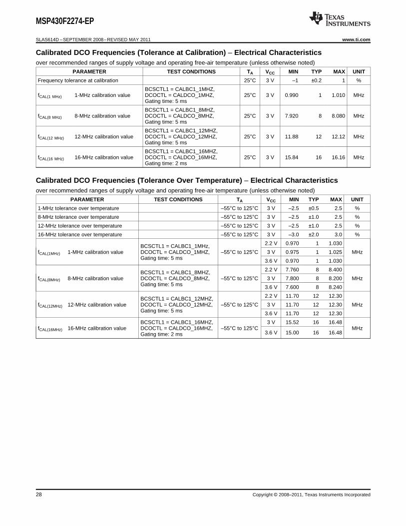
Calibrated DCO Frequencies (Tolerance at Calibration) – Electrical Characteristicsover recommended ranges of supply voltage and operating free-air temperature (unless otherwise noted)
PARAMETER TEST CONDITIONS TA VCC MIN TYP MAX UNIT
Frequency tolerance at calibration 25°C 3 V –1 ±0.2 1 %
BCSCTL1 = CALBC1_1MHZ,fCAL(1 MHz) 1-MHz calibration value DCOCTL = CALDCO_1MHZ, 25°C 3 V 0.990 1 1.010 MHz
Gating time: 5 ms
BCSCTL1 = CALBC1_8MHZ,fCAL(8 MHz) 8-MHz calibration value DCOCTL = CALDCO_8MHZ, 25°C 3 V 7.920 8 8.080 MHz
Gating time: 5 ms
BCSCTL1 = CALBC1_12MHZ,fCAL(12 MHz) 12-MHz calibration value DCOCTL = CALDCO_12MHZ, 25°C 3 V 11.88 12 12.12 MHz
Gating time: 5 ms
BCSCTL1 = CALBC1_16MHZ,fCAL(16 MHz) 16-MHz calibration value DCOCTL = CALDCO_16MHZ, 25°C 3 V 15.84 16 16.16 MHz
Gating time: 2 ms
Calibrated DCO Frequencies (Tolerance Over Temperature) – Electrical Characteristicsover recommended ranges of supply voltage and operating free-air temperature (unless otherwise noted)
PARAMETER TEST CONDITIONS TA VCC MIN TYP MAX UNIT
1-MHz tolerance over temperature –55°C to 125°C 3 V –2.5 ±0.5 2.5 %
8-MHz tolerance over temperature –55°C to 125°C 3 V –2.5 ±1.0 2.5 %
12-MHz tolerance over temperature –55°C to 125°C 3 V –2.5 ±1.0 2.5 %
16-MHz tolerance over temperature –55°C to 125°C 3 V –3.0 ±2.0 3.0 %
2.2 V 0.970 1 1.030BCSCTL1 = CALBC1_1MHz,fCAL(1MHz) 1-MHz calibration value DCOCTL = CALDCO_1MHZ, –55°C to 125°C 3 V 0.975 1 1.025 MHz
Gating time: 5 ms 3.6 V 0.970 1 1.030
2.2 V 7.760 8 8.400BCSCTL1 = CALBC1_8MHZ,fCAL(8MHz) 8-MHz calibration value DCOCTL = CALDCO_8MHZ, –55°C to 125°C 3 V 7.800 8 8.200 MHz
Gating time: 5 ms 3.6 V 7.600 8 8.240
2.2 V 11.70 12 12.30BCSCTL1 = CALBC1_12MHZ,fCAL(12MHz) 12-MHz calibration value DCOCTL = CALDCO_12MHZ, –55°C to 125°C 3 V 11.70 12 12.30 MHz
Gating time: 5 ms 3.6 V 11.70 12 12.30
BCSCTL1 = CALBC1_16MHZ, 3 V 15.52 16 16.48fCAL(16MHz) 16-MHz calibration value DCOCTL = CALDCO_16MHZ, –55°C to 125°C MHz
3.6 V 15.00 16 16.48Gating time: 2 ms
28 Copyright © 2008–2011, Texas Instruments Incorporated

MSP430F2274-EP
www.ti.com SLAS614D –SEPTEMBER 2008–REVISED MAY 2011
Calibrated DCO Frequencies (Tolerance Over Supply Voltage VCC) – Electrical Characteristicsover recommended ranges of supply voltage and operating free-air temperature (unless otherwise noted)
PARAMETER TEST CONDITIONS TA VCC MIN TYP MAX UNIT
1-MHz tolerance over VCC 25°C 1.8 V to 3.6 V –3 ±2 3 %
8-MHz tolerance overVCC 25°C 1.8 V to 3.6 V –3 ±2 3 %
12-MHz tolerance over VCC 25°C 2.2 V to 3.6 V –3 ±2 3 %
16-MHz tolerance over VCC 25°C 3 V to 3.6 V –6 ±2 3 %
BCSCTL1 = CALBC1_1MHZ,1-MHzfCAL(1MHz) DCOCTL = CALDCO_1MHZ, 25°C 1.8 V to 3.6 V 0.970 1 1.030 MHzcalibration value Gating time: 5 ms
BCSCTL1 = CALBC1_8MHZ,8-MHzfCAL(8MHz) DCOCTL = CALDCO_8MHZ, 25°C 1.8 V to 3.6 V 7.760 8 8.240 MHzcalibration value Gating time: 5 ms
BCSCTL1 = CALBC1_12MHZ,12-MHzfCAL(12MHz) DCOCTL = CALDCO_12MHZ, 25°C 2.2 V to 3.6 V 11.64 12 12.36 MHzcalibration value Gating time: 5 ms
BCSCTL1 = CALBC1_16MHZ,16-MHzfCAL(16MHz) DCOCTL = CALDCO_16MHZ, 25°C 3 V to 3.6 V 15.00 16 16.48 MHzcalibration value Gating time: 2 ms
Calibrated DCO Frequencies (Overall Tolerance) – Electrical Characteristicsover recommended ranges of supply voltage and operating free-air temperature (unless otherwise noted)
PARAMETER TEST CONDITIONS TA VCC MIN TYP MAX UNIT
1-MHz tolerance –55°C to 125°C 1.8 V to 3.6 V -5 ±2 +5 %over temperature
8-MHz tolerance –55°C to 125°C 1.8 V to 3.6 V -5 ±2 +5 %over temperature
12-MHz tolerance –55°C to 125°C 2.2 V to 3.6 V -5 ±2 +5 %over temperature
16-MHz tolerance –55°C to 125°C 3 V to 3.6 V -6 ±3 +6 %over temperature
BCSCTL1 = CALBC1_1MHZ,1-MHzfCAL(1MHz) DCOCTL = CALDCO_1MHZ, –55°C to 125°C 1.8 V to 3.6 V .950 1 1.050 MHzcalibration value Gating time: 5 ms
BCSCTL1 = CALBC1_8MHZ,8-MHzfCAL(8MHz) DCOCTL = CALDCO_8MHZ, –55°C to 125°C 1.8 V to 3.6 V 7.6 8 8.4 MHzcalibration value Gating time: 5 ms
BCSCTL1 = CALBC1_12MHZ,12-MHzfCAL(12MHz) DCOCTL = CALDCO_12MHZ, –55°C to 125°C 2.2 V to 3.6 V 11.4 12 12.6 MHzcalibration value Gating time: 5 ms
BCSCTL1 = CALBC1_16MHZ,16-MHzfCAL(16MHz) DCOCTL = CALDCO_16MHZ, –55°C to 125°C 3 V to 3.6 V 15.00 16 17.00 MHzcalibration value Gating time: 2 ms
Copyright © 2008–2011, Texas Instruments Incorporated 29

TA − Temperature − °C
0.97
0.98
0.99
1.00
1.01
1.02
1.03
−50.0 −25.0 0.0 25.0 50.0 75.0 100.0
Fre
quen
cy −
MH
z
VCC = 1.8 V
VCC = 2.2 VVCC = 3.0 V
VCC = 3.6 V
VCC - Suppl y Voltage - V
0.97
0.98
0.99
1.00
1.01
1.02
1.03
1.5 2.0 2.5 3.0 3.5 4.0
Fre
qu
en
cy
- M
Hz
TA = -40 °C
TA = 25 °C
TA = 85 °C
TA = 125 °C
MSP430F2274-EP
SLAS614D –SEPTEMBER 2008–REVISED MAY 2011 www.ti.com
Typical Characteristics – Calibrated 1-MHz DCO Frequency
Figure 11. Calibrated 1-MHz Frequency vs Figure 12. Calibrated 1-MHz Frequency vs VCCTemperature
Wake-Up From Lower-Power Modes (LPM3/4) – Electrical Characteristicsover recommended ranges of supply voltage and operating free-air temperature (unless otherwise noted)
PARAMETER TEST CONDITIONS TA VCC MIN TYP MAX UNIT
BCSCTL1 =CALBC1_1MHZ, –55°C to 125°C 2.2 V/3 V 2DCOCTL =CALDCO_1MHZ,
BCSCTL1 =CALBC1_8MHZ, –55°C to 125°C 2.2 V/3 V 1.5DCOCTL =CALDCO_8MHZ,DCO clock wake-up timetDCO,LPM3/4 μsfrom LPM3/4 (1)BCSCTL1 =CALBC1_12MHZ, –55°C to 125°C 3 V 1DCOCTL =CALDCO_12MHZ,
BCSCTL1 =CALBC1_16MHZ, –55°C to 125°C 3 V 1DCOCTL =CALDCO_16MHZ,
1/fMCLCPU wake-up time from K +tCPU,LPM3/4 LPM3/4 (2) tClock,L
PM3/4
(1) The DCO clock wake-up time is measured from the edge of an external wake-up signal (e.g., port interrupt) to the first clock edgeobservable externally on a clock pin (MCLK or SMCLK).
(2) Parameter applicable only if DCOCLK is used for MCLK.
30 Copyright © 2008–2011, Texas Instruments Incorporated

DCO Frequency − MHz
0.10
1.00
10.00
0.10 1.00 10.00
DC
O W
ake
Tim
e −
usRSELx = 0...11
RSELx = 12...15
MSP430F2274-EP
www.ti.com SLAS614D –SEPTEMBER 2008–REVISED MAY 2011
Typical Characteristics – DCO Clock Wake-Up Time From LPM3/4
Figure 13. Clock Wake-Up Time From LPM3 vs DCO Frequency
DCO With External Resistor ROSC – Electrical Characteristics (1)
over recommended ranges of supply voltage and operating free-air temperature (unless otherwise noted)
PARAMETER TEST CONDITIONS VCC TYP UNIT
2.2 V 1.8DCOR = 1, RSELx = 4, DCOx = 3, MODx = 0,fDCO,ROSC DCO output frequency with ROSC MHzTA = 25°C 3 V 1.95
Dt Temperature drift DCOR = 1, RSELx = 4, DCOx = 3, MODx = 0 2.2 V/3 V ±0.1 %/°CDV Drift with VCC DCOR = 1, RSELx = 4, DCOx = 3, MODx = 0 2.2 V/3 V 10 %/V
(1) ROSC = 100kΩ. Metal film resistor, type 0257. 0.6 watt with 1% tolerance and TK = ±50ppm/°C
Copyright © 2008–2011, Texas Instruments Incorporated 31

0.01
0.10
1.00
10.00
10.00 100.00 1000.00 10000.00
ROSC − External Resistor − k
DC
O F
requ
ency
− M
Hz
RSELx = 4
0.01
0.10
1.00
10.00
10.00 100.00 1000.00 10000.00
ROSC − External Resistor − k
DC
O F
requ
ency
− M
Hz
RSELx = 4
0.00
0.25
0.50
0.75
1.00
1.25
1.50
1.75
2.00
2.25
2.50
−50.0 −25.0 0.0 25.0 50.0 75.0 100.0
TA − Temperature − C
DC
O F
requ
ency
− M
Hz
ROSC = 100k
ROSC = 270k
ROSC = 1M
0.00
0.25
0.50
0.75
1.00
1.25
1.50
1.75
2.00
2.25
2.50
2.0 2.5 3.0 3.5 4.0
VCC − Supply V oltage − V
DC
O F
requ
ency
− M
Hz
ROSC = 100k
ROSC = 270k
ROSC = 1M
MSP430F2274-EP
SLAS614D –SEPTEMBER 2008–REVISED MAY 2011 www.ti.com
Typical Characteristics - DCO With External Resistor ROSC
Figure 14. DCO Frequency vs ROSC, Figure 15. DCO Frequency vs ROSC,VCC = 2.2 V, TA = 25°C VCC = 3.0 V, TA = 25°C
Figure 16. DCO Frequency vs Temperature, VCC = Figure 17. DCO Frequency vs VCC, TA = 25°C3.0 V
32 Copyright © 2008–2011, Texas Instruments Incorporated

MSP430F2274-EP
www.ti.com SLAS614D –SEPTEMBER 2008–REVISED MAY 2011
Crystal Oscillator (LFXT1) Low-Frequency Modes – Electrical Characteristics (1) (2)
over recommended ranges of supply voltage and operating free-air temperature (unless otherwise noted)
PARAMETER TEST CONDITIONS TA VCC MIN TYP MAX UNIT
LFXT1 oscillator –55°C tofLFXT1,LF crystal frequency, LF XTS = 0, LFXT1Sx = 0 or 1 1.8 V to 3.6 V 32,768 Hz105°Cmode 0, 1
LFXT1 oscillatorfLFXT1,LF, logic-level –55°C toXTS = 0, LFXT1Sx = 3 1.8 V to 3.6 V 10,000 32,768 50,000 Hzlogic square-wave input 125°C
frequency, LF mode
XTS = 0, LFXT1Sx = 0; –55°C tofLFXT1,LF = 32,768 kHz, 500105°CCL,eff = 6 pFOscillation allowanceOALF kΩfor LF crystals XTS = 0, LFXT1Sx = 0; –55°C tofLFXT1,LF = 32,768 kHz, 200105°CCL,eff = 12 pF
XCAPx = 0 1Integrated effective XCAPx = 1 5.5–55°C toCL,eff load capacitance, XTS = 0 pF105°CXCAPx = 2 8.5LF mode (3)
XCAPx = 3 11
XTS = 0, Measured atDuty –55°C toLF mode P1.4/ACLK, 2.2 V/3 V 30 50 70 %Cycle 125°CfLFXT1,LF = 32,768 Hz
Oscillator fault –55°C tofFault,LF frequency threshold, XTS = 0, LFXT1Sx = 3 (5) 2.2 V/3 V 10 10,000 Hz125°CLF mode (4)
(1) To improve EMI on the LFXT1 oscillator the following guidelines should be observed:(a) Keep as short of a trace as possible between the device and the crystal.(b) Design a good ground plane around the oscillator pins.(c) Prevent crosstalk from other clock or data lines into oscillator pins XIN and XOUT.(d) Avoid running PCB traces underneath or adjacent to the XIN and XOUT pins.(e) Use assembly materials and praxis to avoid any parasitic load on the oscillator XIN and XOUT pins.(f) If conformal coating is used, ensure that it does not induce capacitive/resistive leakage between the oscillator pins.(g) Do not route the XOUT line to the JTAG header to support the serial programming adapter as shown in other documentation. This
signal is no longer required for the serial programming adapter.(2) Use of the LFXT1 Crystal Oscillator with TA > 105°C is not guaranteed. It is recommended that an external digital clock source or the
internal DCO is used to provide clocking.(3) Includes parasitic bond and package capacitance (approximately 2 pF per pin). Since the PCB adds additional capacitance it is
recommended to verify the correct load by measuring the ACLK frequency. For a correct setup the effective load capacitance shouldalways match the specification of the used crystal.
(4) Frequencies below the MIN specification set the fault flag, frequencies above the MAX specification do not set the fault flag.Frequencies in between might set the flag.
(5) Measured with logic-level input frequency, but also applies to operation with crystals with TA < 105°C.
Internal Very-Low-Power, Low-Frequency Oscillator (VLO) – Electrical Characteristicsover recommended ranges of supply voltage and operating free-air temperature (unless otherwise noted)
TESTPARAMETER TA VCC MIN TYP MAX UNITCONDITIONS
–55°C to 85°C 2.2 V/3 V 4 12 20fVLO VLO frequency kHz
125°C 2.2 V/3 V 22
dfVLO/dT VLO frequency temperature drift (1) –55°C to 125°C 2.2 V/3 V 0.5 %/°C1.8 V –dfVLO/dVCC VLO frequency supply voltage drift (2) 25°C 4 %/V3.6V
(1) Calculated using the box method:I Version: [MAX(–55...85°C) – MIN(–55...85°C)]/MIN(55–...85°C)/[85°C – (–55°C)]T Version: [MAX(–55...125°C) – MIN(–55...125°C)]/MIN(–55...125°C)/[125°C – (–55°C)]
(2) Calculated using the box method: [MAX(1.8...3.6 V) – MIN(1.8...3.6 V)]/MIN(1.8...3.6 V)/(3.6 V – 1.8 V)
Copyright © 2008–2011, Texas Instruments Incorporated 33

MSP430F2274-EP
SLAS614D –SEPTEMBER 2008–REVISED MAY 2011 www.ti.com
Crystal Oscillator (LFXT1) High Frequency Modes – Electrical Characteristics (1) (2)
over recommended ranges of supply voltage and operating free-air temperature (unless otherwise noted)
PARAMETER TEST CONDITIONS TA VCC MIN TYP MAX UNIT
fLFXT1, LFXT1 oscillator crystal frequency, XTS = 1, LFXT1Sx = 0 –55°C to 125°C 1.8 V to 3.6 V 0.4 1 MHzHF0 HF mode 0
fLFXT1, LFXT1 oscillator lcrystal frequency, XTS = 1, LFXT1Sx = 1 –55°C to 125°C 1.8 V to 3.6 V 1 4 MHzHF1 HF mode 1
1.8 V to 3.6 V 2 10fLFXT1, LFXT1 oscillator crystal frequency, XTS = 1, LFXT1Sx = 2 –55°C to 125°C 2.2 V to 3.6 V 2 12 MHzHF2 HF mode 2
3 V to 3.6 V 2 16
1.8 V to 3.6 V 0.4 10LFXT1 oscillator logic-levelfLFXT1, square-wave input frequency, XTS = 1, LFXT1Sx = 3 –55°C to 125°C 2.2 V to 3.6 V 0.4 12 MHzHF,logic HF mode 3 V to 3.6 V 0.4 16
XTS = 0, LFXT1Sx = 0;fLFXT1,HF = 1 MHz, 2700CL,eff = 15 pF
Oscillation allowance for HF XTS = 0, LFXT1Sx = 1OAHF crystals fLFXT1,HF = 4 MHz, –55°C to 125°C 800 Ω
(see Figure 18 and Figure 19) CL,eff = 15 pF
XTS = 0, LFXT1Sx = 2fLFXT1,HF = 16 MHz, 300CL,eff = 15 pF
Integrated effective loadCL,eff capacitance, XTS = 1 (4) –55°C to 125°C 1 pF
HF mode (3)
XTS = 1, Measured atP1.4/ACLK, –55°C to 125°C 40 50 60fLFXT1,HF = 10 MHzDuty HF mode 2.2 V/3 V %Cycle XTS = 1, Measured atP1.4/ACLK, –55°C to 125°C 40 50 60fLFXT1,HF = 16 MHz
Oscillator fault frequency, HF modefFault,HF XTS = 1, LFXT1Sx = 3 (6) –55°C to 125°C 2.2 V/3 V 30 300 kHz(5)
(1) To improve EMI on the LFXT1 oscillator the following guidelines should be observed:(a) Keep as short of a trace as possible between the device and the crystal.(b) Design a good ground plane around the oscillator pins.(c) Prevent crosstalk from other clock or data lines into oscillator pins XIN and XOUT.(d) Avoid running PCB traces underneath or adjacent to the XIN and XOUT pins.(e) Use assembly materials and praxis to avoid any parasitic load on the oscillator XIN and XOUT pins.(f) If conformal coating is used, ensure that it does not induce capacitive/resistive leakage between the oscillator pins.(g) Do not route the XOUT line to the JTAG header to support the serial programming adapter as shown in other documentation. This
signal is no longer required for the serial programming adapter.(2) Use of the LFXT1 Crystal Oscillator with TA > 105°C is not guaranteed. It is recommended that an external digital clock source or the
internal DCO is used to provide clocking.(3) Includes parasitic bond and package capacitance (approximately 2 pF per pin). Since the PCB adds additional capacitance it is
recommended to verify the correct load by measuring the ACLK frequency. For a correct setup the effective load capacitance shouldalways match the specification of the used crystal.
(4) Requires external capacitors at both terminals. Values are specified by crystal manufacturers.(5) Frequencies below the MIN specification set the fault flag, frequencies above the MAX specification do not set the fault flag.
Frequencies in between might set the flag.(6) Measured with logic-level input frequency, but also applies to operation with crystals
34 Copyright © 2008–2011, Texas Instruments Incorporated

Crystal Frequency − MHz
10.00
100.00
1000.00
10000.00
100000.00
0.10 1.00 10.00 100.00
LFXT1Sx = 1
LFXT1Sx = 3
LFXT1Sx = 2
Osc
illat
ion
Allo
wan
ce –
0.0
100.0
200.0
300.0
400.0
500.0
600.0
700.0
800.0
0.0 4.0 8.0 12.0 16.0 20.0
Crystal Frequency − MHz
XT
Osc
illat
or S
uppl
y C
urre
nt −
uA
LFXT1Sx = 1
LFXT1Sx = 3
LFXT1Sx = 2
MSP430F2274-EP
www.ti.com SLAS614D –SEPTEMBER 2008–REVISED MAY 2011
Typical Characteristics – LFXT1 Oscillator in HF Mode (XTS = 1)
Figure 18. Oscillation Allowance vs Crystal Figure 19. XT Oscillator Supply Current vs CrystalFrequency, CL,eff = 15 pF, TA = 25°C Frequency, CL,eff = 15 pF, TA = 25°C
Timer_A – Electrical Characteristicsover recommended ranges of supply voltage and operating free-air temperature (unless otherwise noted)
PARAMETER TEST CONDITIONS TA VCC MIN MAX UNIT
Internal: SMCLK, ACLK, 2.2 V 10fTA Timer_A clock frequency External: TACLK, INCLK, –55°C to 125°C MHz
3 V 16Duty cycle = 50% ± 10%
tTA,cap Timer_A, capture timing TA0, TA1, TA2 –55°C to 125°C 2.2 V/3 V 20 ns
Timer_B – Electrical Characteristicsover recommended ranges of supply voltage and operating free-air temperature (unless otherwise noted)
PARAMETER TEST CONDITIONS TA VCC MIN MAX UNIT
Internal: SMCLK, ACLK, 2.2 V 10fTB Timer_B clock frequency External: TBCLK, –55°C to 125°C MHz
3 V 16Duty Cycle = 50% ± 10%
tTB,cap Timer_B, capture timing TB0, TB1, TB2 –55°C to 125°C 2.2 V/3 V 20 ns
Copyright © 2008–2011, Texas Instruments Incorporated 35

MSP430F2274-EP
SLAS614D –SEPTEMBER 2008–REVISED MAY 2011 www.ti.com
USCI (UART Mode) – Electrical Characteristicsover recommended ranges of supply voltage and operating free-air temperature (unless otherwise noted)
PARAMETER TEST CONDITIONS TA VCC MIN TYP MAX UNIT
Internal: SMCLK, ACLK, fSYSTEfUSCI USCI input clock frequency External: UCLK; –55°C to 125°C MHzMDuty cycle = 50% ± 10%
BITCLK clock frequencyfBITCLK –55°C to 125°C 2.2 V/3 V 1 MHz(equals baud rate in MBaud)
2.2 V 50 150 600tτ UART receive deglitch time (1) –55°C to 125°C ns
3 V 50 150 600
(1) Pulses on the UART receive input (UCxRX) shorter than the UART receive deglitch time are suppressed. To ensure that pulses arecorrectly recognized, their width should exceed the maximum specification of the deglitch time.
USCI (SPI Master Mode) – Electrical Characteristicsover recommended ranges of supply voltage and operating free-air temperature (unless otherwise noted) (see Figure 20 andFigure 21)
PARAMETER TEST CONDITIONS TA VCC MIN MAX UNIT
SMCLK, ACLK,fUSCI USCI input clock frequency –55°C to 125°C fSYSTEM MHzDuty cycle = 50% ± 10%
2.2 V 110tSU,MI SOMI input data setup time –55°C to 125°C ns
3 V 75
2.2 V 0tHD,MI SOMI input data hold time –55°C to 125°C ns
3 V 0
2.2 V 30UCLK edge to SIMO valid,tVALID,MO SIMO output data valid time –55°C to 125°C nsCL = 20 pF 3 V 20
USCI (SPI Slave Mode) – Electrical Characteristicsover recommended ranges of supply voltage and operating free-air temperature (unless otherwise noted) (see Figure 22 andFigure 23)
PARAMETER TEST CONDITIONS TA VCC MIN TYP MAX UNIT
STE lead time,tSTE,LEAD 2.2 V/3 V 50 nsSTE low to clock
STE lag time,tSTE,LAG –55°C to 125°C 2.2 V/3 V 10 nsLast clock to STE high
STE access time,tSTE,ACC 2.2 V/3 V 50 nsSTE low to SOMI data out
STE disable time,tSTE,DIS STE high to SOMI high 2.2 V/3 V 50 ns
impedance
2.2 V 20tSU,SI SIMO input data setup time –55°C to 125°C ns
3 V 15
2.2 V 10tHD,SI SIMO input data hold time –55°C to 125°C ns
3 V 10
2.2 V 75 110UCLK edge to SOMI valid,tVALID,SO SOMI output data valid time –55°C to 125°C nsCL = 20 pF 3 V 50 75
36 Copyright © 2008–2011, Texas Instruments Incorporated

UCLK
SCMI
SIMO
CKPL = 0
CKPL = 1
1/fUCxCLK
tLOW/HIGH tLOW/HIGH tSU,MI
tHD,MI
tVALID, MO
UCLK
SCMI
SIMO
CKPL = 0
CKPL = 1
1/fUCxCLK
tLOW/HIGH tLOW/HIGH
tSU,MItHD,MI
tVALID, MO
MSP430F2274-EP
www.ti.com SLAS614D –SEPTEMBER 2008–REVISED MAY 2011
Figure 20. SPI Master Mode, CKPH = 0
Figure 21. SPI Master Mode, CKPH = 1
Copyright © 2008–2011, Texas Instruments Incorporated 37

STE
UCLK
SIMO
SOMI
CKPL = 0
CKPL = 1
1/fUCxCLK
tSTE,LEAD
tLOW,HIGH tLOW,HIGH
tACC
tSTE,LAG
tSU,SIMO
tHD,SIMO
tVALID,SOMI tDIS
,
STE
UCLK
SIMO
SOMI
CKPL = 0
CKPL = 1
1/fUCxCLK
tSTE,LEAD
tLOW,HIGH tLOW,HIGH
tACC
tSTE,LAG
tDIS
tSU,SI
tVALID,SO
tHD,SI
MSP430F2274-EP
SLAS614D –SEPTEMBER 2008–REVISED MAY 2011 www.ti.com
Figure 22. SPI Slave Mode, CKPH = 0
Figure 23. SPI Slave Mode, CKPH = 1
38 Copyright © 2008–2011, Texas Instruments Incorporated

SDA
SCL
tLOW
tHD ,DAT
tSU ,DAT
tHD ,STA tSU ,STA tHD ,STA
tHIGH
tSU , STO
tSP
tBUF
MSP430F2274-EP
www.ti.com SLAS614D –SEPTEMBER 2008–REVISED MAY 2011
USCI (I2C Mode) – Electrical Characteristicsover recommended ranges of supply voltage and operating free-air temperature (unless otherwise noted) (see Figure 24)
PARAMETER TEST CONDITIONS TA VCC MIN TYP MAX UNIT
Internal: SMCLK, ACLK, fSYSTfUSCI USCI input clock frequency External: UCLK, MHzEMDuty cycle = 50% ± 10%
fSCL SCL clock frequency –55°C to 125°C 2.2 V/3 V 0 400 kHz
fSCL ≤ 100 kHz –55°C to 125°C 4.0tHD,STA Hold time (repeated) START 2.2 V/3 V μs
fSCL > 100 kHz –55°C to 125°C 0.6
fSCL ≤ 100 kHz –55°C to 125°C 4.7Set-up time for a repeatedtSU,STA 2.2 V/3 V μsSTART fSCL > 100 kHz –55°C to 125°C 0.6
tHD,DAT Data hold time –55°C to 125°C 2.2 V/3 V 0 ns
tSU,DAT Data set-up time –55°C to 125°C 2.2 V/3 V 250 ns
tSU,STO Set-up time for STOP –55°C to 125°C 2.2 V/3 V 4.0 μs
2.2 V 50 150 600Pulse width of spikestSP –55°C to 125°C nssuppressed by input filter 3 V 50 100 600
Figure 24. I2C Mode Timing
Copyright © 2008–2011, Texas Instruments Incorporated 39

MSP430F2274-EP
SLAS614D –SEPTEMBER 2008–REVISED MAY 2011 www.ti.com
10-Bit ADC, Power-Supply and Input Range Conditions – Electrical Characteristics (1)
over recommended ranges of supply voltage and operating free-air temperature (unless otherwise noted)
PARAMETER TEST CONDITIONS TA VCC MIN TYP MAX UNIT
VCC Analog supply voltage range VSS = 0 V –55°C to125 °C 2.2 3.6 V
All Ax terminals,VAx Analog input voltage range (2) Analog inputs selected in –55°C to 125°C 0 VCC V
ADC10AE register
fADC10CLK = 5.0 MHz, 2.2 V 0.52 1.05ADC10ON = 1, REFON = 0,
IADC10 ADC10 supply current (3) ADC10SHT0 = 1, –55°C to 125°C mA3 V 0.6 1.2ADC10SHT1 = 0,
ADC10DIV = 0
fADC10CLK = 5.0 MHz,ADC10ON = 0, REF2_5V = 0, –55°C to 125°C 2.2 V/3 VREFON = 1, REFOUT = 0Reference supply current,IREF+ 0.25 .4 mAreference buffer disabled (4)fADC10CLK = 5.0 MHz,ADC10ON = 0, REF2_5V = 1, –55°C to 125°C 3 VREFON = 1, REFOUT = 0
fADC10CLK = 5.0 MHz, –55°C to 85°C 2.2 V/3 V 1.1 1.4Reference buffer supply current ADC10ON = 0, REFON = 1,IREFB,0 mAwith ADC10SR = 0 (4) REF2_5V = 0, 125°C 2.2 V/3 V 1.8
REFOUT = 1, ADC10SR = 0
fADC10CLK = 5.0 MHz, –55°C to 85°C 2.2 V/3 V 0.5 .7 mAReference buffer supply current ADC10ON = 0, REFON = 1,IREFB,1 with ADC10SR = 1 (4) REF2_5V = 0, REFOUT = 1, 125°C 2.2 V/3 V .8 mA
ADC10SR=1
Only one terminal Ax selected atCI Input capacitance 27 pFa time
RI Input MUX ON resistance 0 V ≤ VAx ≤ VCC 2.2 V/3 V 2000 Ω
(1) The leakage current is defined in the leakage current table with Px.x/Ax parameter.(2) The analog input voltage range must be within the selected reference voltage range VR+ to VR– for valid conversion results.(3) The internal reference supply current is not included in current consumption parameter IADC10.(4) The internal reference current is supplied via terminal VCC. Consumption is independent of the ADC10ON control bit, unless a
conversion is active. The REFON bit enables the built-in reference to settle before starting an A/D conversion.
40 Copyright © 2008–2011, Texas Instruments Incorporated

MSP430F2274-EP
www.ti.com SLAS614D –SEPTEMBER 2008–REVISED MAY 2011
10-Bit ADC, Built-In Voltage Reference – Electrical Characteristicsover recommended ranges of supply voltage and operating free-air temperature (unless otherwise noted)
PARAMETER TEST CONDITIONS TA VCC MIN TYP MAX UNIT
IVREF+ ≤ 1 mA, REF2_5V = 0 –55°C to 125°C 2.2Positive built-inVCC,REF+ reference analog IVREF+ ≤ 0.5 mA, REF2_5V = 1 –55°C to 125°C 2.8 V
supply voltage range IVREF+ ≤ 1 mA, REF2_5V = 1 –55°C to 125°C 2.9
IVREF+ ≤ IVREF+max, REF2_5V = 0 –55°C to 125°C 2.2 V/3 V 1.41 1.5 1.59Positive built-inVREF+ Vreference voltage IVREF+ ≤ IVREF+max, REF2_5V = 1 –55°C to 125°C 3 V 2.35 2.5 2.65
2.2 V ±0.5Maximum VREF+ loadILD,VREF+ –55°C to 125°C mAcurrent 3 V ±1
IVREF+ = 500 μA ± 100 μA,Analog input voltage VAx ≉ 0.75 V, –55°C to 125°C 2.2 V/3 V ±2REF2_5V = 0
VREF+ load regulation LSBIVREF+ = 500 μA ± 100 μA,Analog input voltage VAx ≉ 1.25 V, –55°C to 125°C 3 V ±2REF2_5V = 1
IVREF+ = 100 μA→900 ADC10SR = 0 –55°C to 125°C 400μA,VREF+ load regulation VAx ≉ 0.5 × VREF+, 3 V nsresponse time ADC10SR = 1 –55°C to 125°C 2000Error of conversionresult ≤ 1 LSB
Maximum capacitance IVREF+ ≤ = 1 mA,CVREF+ –55°C to 125°C 2.2 V/3 V 100 pFat pin VREF+(1) REFON = 1, REFOUT = 1
Temperature IVREF+ = const. with ppm/°TCREF+ –55°C to 125°C 2.2 V/3 V ±100coefficient 0 mA ≤ IVREF+ ≤ 1 mA C
Settling time of internal IVREF+ = 0.5 mA, REF2_5V = 0tREFON –55°C to 125°C 3.6 V 30 μsreference voltage (2) REFON = 0 → 1
IVREF+ = 0.5 mA, ADC10SR = 0 –55°C to 125°C 1REF2_5V = 0, 2.2 VREFON = 1, ADC10SR = 1 –55°C to 125°C 2.5REFBURST = 1Settling time oftREFBURST μsreference buffer (2)IVREF+ = 0.5 mA, ADC10SR = 0 –55°C to 125°C 2REF2_5V = 1, 3 VREFON = 1, ADC10SR = 1 –55°C to 125°C 4.5REFBURST = 1
(1) The capacitance applied to the internal buffer operational amplifier, if switched to terminal P2.4/TA2/A4/VREF+/VeREF+ (REFOUT = 1),must be limited; the reference buffer may become unstable otherwise.
(2) The condition is that the error in a conversion started after tREFON or tRefBuf is less than ±0.5 LSB.
Copyright © 2008–2011, Texas Instruments Incorporated 41

MSP430F2274-EP
SLAS614D –SEPTEMBER 2008–REVISED MAY 2011 www.ti.com
10-Bit ADC, External Reference – Electrical Characteristics (1)
over recommended ranges of supply voltage and operating free-air temperature (unless otherwise noted)
PARAMETER TEST CONDITIONS TA VCC MIN MAX UNIT
VeREF+ > VeREF–, –55°C to 125°C 1.4 VCCSREF1 = 1, SREF0 = 0Positive external reference inputVeREF+ Vvoltage range (2)VeREF– ≤ VeREF+ ≤ VCC – 0.15 –55°C to 125°C 1.4 3.0V,SREF1 = 1, SREF0 = 1 (3)
Negative external reference inputVeREF– VeREF+ > VeREF– –55°C to 125°C 0 1.2 Vvoltage range (4)
Differential external referenceΔVeREF input voltage range, VeREF+ > VeREF–
(5) –55°C to 125°C 1.4 VCC VΔVeREF = VeREF+ – VeREF–
0 V ≤ VeREF+ ≤ VCC, –55°C to 125°C 2.2 V/3 V ±1SREF1 = 1, SREF0 = 0IVeREF+ Static input current into VeREF+ μA0 V ≤ VeREF+ ≤ VCC – 0.15 V ≤ 3
V, –55°C to 125°C 2.2 V/3 V 0SREF1 = 1, SREF0 = 1(3)
IVeREF– Static input current into VeREF– 0 V ≤ VeREF– ≤ VCC –55°C to 125°C 2.2 V/3 V ±1 μA
(1) The external reference is used during conversion to charge and discharge the capacitance array. The input capacitance, CI, is also thedynamic load for an external reference during conversion. The dynamic impedance of the reference supply should follow therecommendations on analog-source impedance to allow the charge to settle for 10-bit accuracy.
(2) The accuracy limits the minimum positive external reference voltage. Lower reference voltage levels may be applied with reducedaccuracy requirements.
(3) Under this condition the external reference is internally buffered. The reference buffer is active and requires the reference buffer supplycurrent IREFB. The current consumption can be limited to the sample and conversion period with REBURST = 1.
(4) The accuracy limits the maximum negative external reference voltage. Higher reference voltage levels may be applied with reducedaccuracy requirements.
(5) The accuracy limits the minimum external differential reference voltage. Lower differential reference voltage levels may be applied withreduced accuracy requirements.
10-Bit ADC, Timing Parameters – Electrical Characteristicsover recommended ranges of supply voltage and operating free-air temperature (unless otherwise noted)
PARAMETER TEST CONDITIONS TA VCC MIN TYP MAX UNIT
For specified ADC10SR=0 –55°C to 125°C 2.2 V/3 V 0.45 6.5ADC10 input clockfADC10CLK performance of ADC10 MHzfrequency ADC10SR=1 –55°C to 125°C 2.2 V/3 V 0.45 1.5linearity parameters
ADC10 built-in ADC10DIVx = 0, ADC10SSELx = 0,fADC10OSC –55°C to 125°C 2.2 V/3 V 3.25 6.45 MHzoscillator frequency fADC10CLK = fADC10OSC
ADC10 built-in oscillator,ADC10SSELx = 0, –55°C to 125°C 2.2 V/3 V 2.06 3.51fADC10CLK = fADC10OSC
tCONVERT Conversion time μs13 =fADC10CLK from ACLK, MCLK, or –55°C to 125°C ADC10DIVxSMCLK: ADC10SSELx ≠ 0 1/fADC10CLK
Turn-on settling timetADC10ON(1)–55°C to 125°C 100 nsof the ADC
(1) The condition is that the error in a conversion started after tADC10ON is less than ±0.5 LSB. The reference and input signal are alreadysettled.
42 Copyright © 2008–2011, Texas Instruments Incorporated

MSP430F2274-EP
www.ti.com SLAS614D –SEPTEMBER 2008–REVISED MAY 2011
10-Bit ADC, Linearity Parameters – Electrical Characteristics (1)
over recommended ranges of supply voltage and operating free-air temperature (unless otherwise noted)
PARAMETER TEST CONDITIONS TA VCC MIN TYP MAX UNIT
EI Integral linearity error –55°C to 125°C 2.2 V/3 V ±1 LSB
ED Differential linearity error –55°C to 125°C 2.2 V/3 V ±1 LSB
EO Offset error Source impedance RS < 100 Ω –55°C to 125°C 2.2 V/3 V ±1 LSB
SREFx = 010, un-buffered externalreference, –55°C to 125°C 2.2 V ±1.1 ±2VeREF+ = 1.5 V
SREFx = 010; un-buffered externalreference, –55°C to 125°C 3 V ±1.1 ±2VeREF+ = 2.5 V
EG Gain error LSBSREFx = 011, buffered externalreference (2), –55°C to 125°C 2.2 V ±1.1 ±4VeREF+ = 1.5 V
SREFx = 011, buffered externalreference (2), –55°C to 125°C 3 V ±1.1 ±3VeREF+ = 2.5 V
SREFx = 010, unbuffered externalreference, –55°C to 125°C 2.2 V ±2 ±5VeREF+ = 1.5 V
SREFx = 010, unbuffered externalreference, –55°C to 125°C 3 V ±2 ±5VeREF+ = 2.5 V
ET Total unadjusted error LSBSREFx = 011, buffered externalreference (2), –55°C to 125°C 2.2 V ±2 ±7VeREF+ = 1.5 V
SREFx = 011, buffered externalreference (2), –55°C to 125°C 3 V ±2 ±6VeREF+ = 2.5 V
(1) 2.2V Not Production Tested.(2) The reference buffer's offset adds to the gain and total unadjusted error.
Copyright © 2008–2011, Texas Instruments Incorporated 43

MSP430F2274-EP
SLAS614D –SEPTEMBER 2008–REVISED MAY 2011 www.ti.com
10-Bit ADC, Temperature Sensor and Built-In VMID – Electrical Characteristicsover recommended ranges of supply voltage and operating free-air temperature (unless otherwise noted)
PARAMETER TEST CONDITIONS TA VCC MIN TYP MAX UNIT
2.2 V 40 120Temperature sensor REFON = 0, INCHx = 0Ah,ISENSOR –55°C to 125°C μAsupply current (1) TA = 25°C 3 V 60 160
ADC10ON = 1,TCSENSOR –55°C to 125°C 2.2 V/3 V 3.44 3.55 3.66 mV/°CINCHx = 0Ah (2)
ADC10ON = 1,VOffset,Sensor Sensor offset voltage –55°C to 125°C -100 100 mVINCHx = 0Ah (2)
Temperature sensor voltageat TA = 125°C (T version –55°C to 125°C 1265 1365 1465only)
Temperature sensor voltage –55°C to 125°C 1195 1295 1395at TA = 85°CVSensor Sensor output voltage (3) 2.2 V/3 V mVTemperature sensor voltage –55°C to 125°C 985 1085 1185at TA = 25°CTemperature sensor voltage –55°C to 125°C 895 995 1095at TA = 0°CADC10ON = 1, INCHx = 0Ah,Sample time requiredtSensor(sample) Error of conversion result –55°C to 125°C 2.2 V/3 V 30 μsif channel 10 is selected (4)≤ 1 LSB
2.2 V NACurrent into dividerIVMID ADC10ON = 1, INCHx = 0Bh –55°C to 125°C μAat channel 11 (5)3 V NA
2.2 V 1.06 1.1 1.14ADC10ON = 1, INCHx = 0Bh,VMID VCC divider at channel 11 –55°C to 125°C VVMID is ≉ 0.5 × VCC 3 V 1.46 1.5 1.54
ADC10ON = 1, INCHx = 0Bh, 2.2 V 1400Sample time requiredtVMID(sample) Error of conversion result –55°C to 125°C nsif channel 11 is selected (6)3 V 1220≤ 1 LSB
(1) The sensor current ISENSOR is consumed if (ADC10ON = 1 and REFON = 1) or (ADC10ON = 1 and INCH = 0Ah and sample signal ishigh). When REFON = 1, ISENSOR is included in IREF+. When REFON = 0, ISENSOR applies during conversion of the temperature sensorinput (INCH = 0Ah).
(2) The following formula can be used to calculate the temperature sensor output voltage:VSensor,typ = TCSensor (273 + T [°C] ) + VOffset,sensor [mV] orVSensor,typ = TCSensor T [°C] + VSensor(TA = 0°C) [mV]
(3) Results based on characterization and/or production test, not TCSensor or VOffset,sensor.(4) The typical equivalent impedance of the sensor is 51 kΩ. The sample time required includes the sensor-on time tSENSOR(on).(5) No additional current is needed. The VMID is used during sampling.(6) The on-time tVMID(on) is included in the sampling time tVMID(sample); no additional on time is needed.
Operational Amplifier (OA) Supply Specifications – Electrical Characteristicsover recommended ranges of supply voltage and operating free-air temperature (unless otherwise noted)
PARAMETER TEST CONDITIONS TA VCC MIN TYP MAX UNIT
VCC Supply voltage range –55°C to 125°C 2.2 3.6 V
Fast Mode –55°C to 125°C 180 290
ICC Supply current (1) Medium Mode –55°C to 125°C 2.2 V/3 V 110 190 μA
Slow Mode –55°C to 125°C 50 80
PSSR Power-supply rejection ratio Noninverting 2.2 V/3 V 70 dB
(1) Corresponding pins configured as OA inputs and outputs, respectively.
44 Copyright © 2008–2011, Texas Instruments Incorporated

RO/P(OAx)Max
0.2V AVCCAVCC −0.2V VOUT
Min
RLoad
AVCC
CLoad
2
ILoad
OAx
O/P(OAx)
MSP430F2274-EP
www.ti.com SLAS614D –SEPTEMBER 2008–REVISED MAY 2011
Operational Amplifier (OA) Input/Output Specifications – Electrical Characteristicsover recommended ranges of supply voltage and operating free-air temperature (unless otherwise noted)
PARAMETER TEST CONDITIONS TA VCC MIN TYP MAX UNIT
VCC -VI/P Input voltage range –55°C to 125°C –0.1 V1.2
–55°C to 55°C –15 ±0.5 15Input leakageIlkg 55°C to 85°C 2.2 V/3 V –20 ±5 20 nAcurrent (1) (2)
85°C to 125°C –100 100
Fast Mode 50
Medium Mode fV(I/P) = 1 kHz 80
Slow Mode 140Voltage noise density,Vn nV/√HzI/P Fast Mode 30
Medium Mode fV(I/P) = 10 kHz 50
Slow Mode 65
VIO Offset voltage, I/P –55°C to 125°C 2.2 V/3 V ±10 mV
Offset temperature See (3) 2.2 V/3 V ±10 μV/°Cdrift, I/P
Offset voltage drift 0.3 V ≤ VIN ≤ VCC – 1.0 V –55°C to 125°C 2.2 V/3 V ±1.5 mV/Vwith supply, I/P ΔVCC ≤ ±10%, TA = 25°CVCC –Fast Mode, ISOURCE ≤ –500 μA –55°C to 125°C VCCHigh-level output 0.2
VOH voltage, 2.2 V/3 V VVCC –O/P Slow Mode, ISOURCE ≤ –150 μA –55°C to 125°C VCC0.1
Low-level output Fast Mode, ISOURCE ≤ 500 μA –55°C to 125°C VSS 0.2VOL voltage, 2.2 V/3 V V
Slow Mode, ISOURCE ≤ 150 μA –55°C to 125°C VSS 0.1O/P
RLoad = 3 kΩ, CLoad = 50 pF, 150VO/P(OAx) < 0.2 V
Output resistance (4) RLoad = 3 kΩ, CLoad = 50 pF,RO/P(OAx) 2.2 V/3 V 150 Ω(see Figure 25) VO/P(OAx) > VCC – 1.2 V
RLoad = 3 kΩ, CLoad = 50 pF, 0.10.2 V ≤ VO/P(OAx) ≤ VCC – 0.2 V
Common-modeCMRR Noninverting 2.2 V/3 V 70 dBrejection ratio
(1) ESD damage can degrade input current leakage.(2) The input bias current is overridden by the input leakage current.(3) Calculated using the box method(4) Specification valid for voltage-follower OAx configuration
Figure 25. OAx Output Resistance Tests
Copyright © 2008–2011, Texas Instruments Incorporated 45

Input Frequency − kHz
−80
−60
−40
−20
0
20
40
60
80
100
120
140
1 10 100 1000 10000 100000
TYPICAL OPEN-LOOP GAIN vs FREQUENCY
Slow Mode
Fast Mode
Gai
n −
dB
Medium Mode
Input Frequency − kHz
−250
−200
−150
−100
−50
0
1 10 100 1000 10000 100000
TYPICAL PHASE vs FREQUENCYP
hase
− d
egre
es
Slow Mode
Fast Mode
Medium Mode
MSP430F2274-EP
SLAS614D –SEPTEMBER 2008–REVISED MAY 2011 www.ti.com
Operational Amplifier (OA) Dynamic Specifications – Electrical Characteristicsover recommended ranges of supply voltage and operating free-air temperature (unless otherwise noted)
PARAMETER TEST CONDITIONS TA VCC MIN TYP MAX UNIT
Fast Mode 1.2
SR Slew rate Medium Mode 0.8 V/μs
Slow Mode 0.3
Open-loop voltage gain 100 dB
φm Phase margin CL = 50 pF 60 deg
Gain margin CL = 50 pF 20 dB
Noninverting, Fast Mode, 2.2RL = 47 kΩ, CL = 50 pF
Gain-bandwidth product Noninverting, Medium Mode,GBW 2.2 V/3 V 1.4 MHz(see Figure 26 and Figure 27) RL = 300 kΩ, CL = 50 pF
Noninverting, Slow Mode, 0.5RL = 300 kΩ, CL = 50 pF
ten(on) Enable time on ton, noninverting, Gain = 1 –55°C to 125°C 2.2 V/3 V 10 20 μs
ten(off) Enable time off –55°C to 125°C 2.2 V/3 V 1 μs
Figure 26. Figure 27.
Operational Amplifier OA Feedback Network, Resistor Network – Electrical Characteristics (1)
over recommended ranges of supply voltage and operating free-air temperature (unless otherwise noted)
PARAMETER TEST CONDITIONS TA MIN TYP MAX UNIT
Total resistance of resistorRtotal 96 kΩstring
Runit Unit resistor of resistor string (2) 6 kΩ
(1) A single resistor string is composed of 4 Runit + 4 Runit + 2 Runit + 2 Runit + 1 Runit + 1 Runit + 1 Runit + 1 Runit = 16 Runit = Rtotal.(2) For the matching (i.e., the relative accuracy) of the unit resistors on a device, refer to the gain and level specifications of the respective
configurations.
46 Copyright © 2008–2011, Texas Instruments Incorporated

MSP430F2274-EP
www.ti.com SLAS614D –SEPTEMBER 2008–REVISED MAY 2011
Operational Amplifier (OA) Feedback Network, Comparator Mode (OAFCx = 3) – ElectricalCharacteristicsover recommended ranges of supply voltage and operating free-air temperature (unless otherwise noted)
PARAMETER TEST CONDITIONS TA VCC MIN TYP MAX UNIT
OAFBRx = 1, OARRIP = 0 –55°C to 125°C 0.242 1/4 0.262
OAFBRx = 2, OARRIP = 0 –55°C to 125°C 0.492 ½ 0.512
OAFBRx = 3, OARRIP = 0 –55°C to 125°C 0.619 5/8 0.639
OAFBRx = 4, OARRIP = 0 N/A (1)
OAFBRx = 5, OARRIP = 0 N/A (1)
OAFBRx = 6, OARRIP = 0 N/A (1)
OAFBRx = 7, OARRIP = 0 N/A (1)
VLevel Comparator level 2.2 V/3 V VCCOAFBRx = 1, OARRIP = 1 –55°C to 125°C 0.057 1/16 0.071
OAFBRx = 2, OARRIP = 1 –55°C to 125°C 0.122 1/8 0.128
OAFBRx = 3, OARRIP = 1 –55°C to 125°C 0.182 3/16 0.197
OAFBRx = 4, OARRIP = 1 –55°C to 125°C 0.242 1/4 0.262
OAFBRx = 5, OARRIP = 1 –55°C to 125°C 0.367 3/8 0.383
OAFBRx = 6, OARRIP = 1 –55°C to 125°C 0.492 ½ 0.512
OAFBRx = 7, OARRIP = 1 N/A (1)
Fast Mode, Overdrive 10 mV 40
Fast Mode, Overdrive 100 mV 4
Fast Mode, Overdrive 500 mV 3
Medium Mode, Overdrive 10 mV 60Propagation delaytPLH, tPHL Medium Mode, Overdrive 100 mV 2.2 V/3 V 6 μs(low-high and high-low)
Medium Mode, Overdrive 500 mV 5
Slow Mode, Overdrive 10 mV 160
Slow Mode, Overdrive 100 mV 20
Slow Mode, Overdrive 500 mV 15
(1) The level is not available due to the analog input voltage range of the operational amplifier.
Operational Amplifier (OA) Feedback Network, Noninverting Amplifier Mode (OAFCx = 4) –Electrical Characteristicsover recommended ranges of supply voltage and operating free-air temperature (unless otherwise noted)
PARAMETER TEST CONDITIONS TA VCC MIN TYP MAX UNIT
OAFBRx = 0 –55°C to 125°C 0.970 1.00 1.035
OAFBRx = 1 –55°C to 125°C 1.325 1.334 1.345
OAFBRx = 2 –55°C to 125°C 1.985 2.001 2.017
OAFBRx = 3 –55°C to 125°C 2.638 2.667 2.696G Gain 2.2 V/3 V
OAFBRx = 4 –55°C to 125°C 3.94 4.00 4.06
OAFBRx = 5 –55°C to 125°C 5.22 5.33 5.44
OAFBRx = 6 –55°C to 125°C 7.76 7.97 8.18
OAFBRx = 7 –55°C to 125°C 15.0 15.8 16.7
2.2 V –60Total harmonicTHD All gains dBdistortion/nonlinearity 3 V –70
tSettle Settling time (1) All power modes –55°C to 125°C 2.2 V/3 V 7 12 μs
(1) The settling time specifies the time until an ADC result is stable. This includes the minimum required sampling time of the ADC. Thesettling time of the amplifier itself might be faster.
Copyright © 2008–2011, Texas Instruments Incorporated 47

MSP430F2274-EP
SLAS614D –SEPTEMBER 2008–REVISED MAY 2011 www.ti.com
Operational Amplifier (OA) Feedback Network, Inverting Amplifier Mode (OAFCx = 6) –Electrical Characteristics (1)
over recommended ranges of supply voltage and operating free-air temperature (unless otherwise noted)
PARAMETER TEST CONDITIONS TA VCC MIN TYP MAX UNIT
OAFBRx = 1 –55°C to 125°C -0.385 –0.335 -0.305
OAFBRx = 2 –55°C to 125°C -1.023 –1.002 -0.979
OAFBRx = 3 –55°C to 125°C -1.712 –1.668 -1.624
G Gain OAFBRx = 4 –55°C to 125°C 2.2 V/3 V -3.10 –3.00 -2.90
OAFBRx = 5 –55°C to 125°C -4.51 –4.33 -4.15
OAFBRx = 6 –55°C to 125°C -7.37 –6.97 -6.57
OAFBRx = 7 –55°C to 125°C -16.6 –14.8 -13.1
2.2 V –60Total harmonicTHD All gains dBdistortion/nonlinearity 3 V –70
tSettle Settling time (2) All power modes –55°C to 125°C 2.2 V/3 V 7 12 μs
(1) This includes the 2 OA configuration "inverting amplifier with input buffer". Both OA needs to be set to the same power mode OAPMx.(2) The settling time specifies the time until an ADC result is stable. This includes the minimum required sampling time of the ADC. The
settling time of the amplifier itself might be faster.
Flash Memory – Electrical Characteristics (1)
over recommended ranges of supply voltage and operating free-air temperature (unless otherwise noted)
PARAMETER TEST TACONDITIO VCC MIN TYP MAX UNIT
NS
VCC(PGM/ERASE) Program and erase supply voltage –55°C to 125°C 2.2 3.6 V
fFTG Flash timing generator frequency –55°C to 125°C 257 476 kHz
IPGM Supply current from VCC during program –55°C to 125°C 2.2 V/3.6 V 1 5 mA
IERASE Supply current from VCC during erase –55°C to 125°C 2.2 V/3.6 V 1 10.5 mA
tCPT Cumulative program time (2) –55°C to 125°C 2.2 V/3.6 V 10 ms
tCMErase Cumulative mass erase time –55°C to 125°C 2.2 V/3.6 V 20 ms
Program/Erase endurance –55°C to 125°C 104 105 cycles
tRetention Data retention duration (3) TJ = 25°C 100 years
tWord Word or byte program time (4) 30 tFTG
tBlock, 0 Block program time for 1st byte or word (4) 25 tFTG
Block program time for each additionaltBlock, 1-63(4) 18 tFTGbyte or word
tBlock, End Block program end-sequence wait time (4) 6 tFTG
1059tMass Erase Mass erase time (4) tFTG3
tSeg Erase Segment erase time (4) 4819 tFTG
(1) Additional Flash retention documentation located in application report (SLAA392).(2) The cumulative program time must not be exceeded when writing to a 64-byte flash block. This parameter applies to all programming
methods: individual word/byte write and block write modes.(3) To test the flash data retention at various temperatures we make use of accelerated tests on the flash with 500-Hours Baking Time at
250°C. These tests are wholly based on Arrhenius law and equation.(4) These values are hardwired into the Flash Controller's state machine (tFTG = 1/fFTG).
RAM – Electrical Characteristicsover recommended ranges of supply voltage and operating free-air temperature (unless otherwise noted)
PARAMETER TEST CONDITIONS TA MIN MAX UNIT
V(RAMh) RAM retention supply voltage (1) CPU halted –55°C to 125°C 1.6 V
(1) This parameter defines the minimum supply voltage VCC when the data in RAM remains unchanged. No program execution shouldhappen during this supply voltage condition.
48 Copyright © 2008–2011, Texas Instruments Incorporated

MSP430F2274-EP
www.ti.com SLAS614D –SEPTEMBER 2008–REVISED MAY 2011
JTAG and Spy-Bi-Wire Interface – Electrical Characteristicsover recommended ranges of supply voltage and operating free-air temperature (unless otherwise noted)
PARAMETER TEST CONDITIONS TA VCC MIN TYP MAX UNIT
fSBW Spy-Bi-Wire input frequency –55°C to 125°C 2.2 V/3 V 0 20 MHz
0.02tSBW,Low Spy-Bi-Wire low clock pulse length –55°C to 125°C 2.2 V/3 V 15 μs5
Spy-Bi-Wire enable timetSBW,En (TEST high to acceptance of first clock –55°C to 125°C 2.2 V/3 V 1 μs
edge (1))
Spy-Bi-Wire return to normal operationtSBW,Ret –55°C to 125°C 2.2 V/3 V 15 100 μstime
2.2 V 0 5 MHzfTCK TCK input frequency (2) –55°C to 125°C
3 V 0 10 MHz
RInternal Internal pulldown resistance on TEST –55°C to 125°C 2.2 V/3 V 25 60 90 kΩ
(1) Tools accessing the Spy-Bi-Wire interface need to wait for the maximum tSBW,En time after pulling the TEST/SBWCLK pin high beforeapplying the first SBWCLK clock edge.
(2) fTCK may be restricted to meet the timing requirements of the module selected.
JTAG Fuse (1) – Electrical Characteristicsover recommended ranges of supply voltage and operating free-air temperature (unless otherwise noted)
PARAMETER TEST CONDITIONS TA MIN MAX UNIT
VCC(FB) Supply voltage during fuse-blow condition TA = 25°C 2.5 V
VFB Voltage level on TEST for fuse blow –55°C to 125°C 6 7 V
IFB Supply current into TEST during fuse blow –55°C to 125°C 100 mA
tFB Time to blow fuse –55°C to 125°C 1 ms
(1) Once the fuse is blown, no further access to the JTAG/Test, Spy-Bi-Wire, and emulation feature is possible, and JTAG is switched tobypass mode.
Copyright © 2008–2011, Texas Instruments Incorporated 49

Direction0: Input1: Output
P1SEL.x
1
0P1DIR.x
P1IN.x
P1IRQ.x
D
EN
Module X IN
1
0
Module X OUT
P1OUT.x
InterruptEdgeSelect
QEN
Set
P1SEL.x
P1IES.x
P1IFG.x
P1IE.x
P1.0/TACLK/ADC10CLKP1.1/TA0P1.2/TA1P1.3/TA2
1
0DVSS
DVCC
P1REN.xPad Logic
1
MSP430F2274-EP
SLAS614D –SEPTEMBER 2008–REVISED MAY 2011 www.ti.com
APPLICATION INFORMATION
Port P1 Pin Schematic: P1.0 to P1.3, Input/Output With Schmitt Trigger
Port P1 (P1.0 to P1.3) Pin Functions
CONTROL BITS/SIGNALS (2)
PIN NAME (P1.X) X FUNCTION (1)
P1DIR.x P1SEL.x
P1.0 (3) I: 0; O: 1 0
P1.0/TACLK/ADC10CLK 0 Timer_A3.TACLK 0 1
ADC10CLK 1 1
P1.1 (4) (I/O) I: 0; O: 1 0
P1.1/TA0 1 Timer_A3.CCI0A 0 1
Timer_A3.TA0 1 1
P1.2 (4) (I/O) I: 0; O: 1 0
P1.2/TA1 2 Timer_A3.CCI0A 0 1
Timer_A3.TA0 1 1
P1.3 (4) I/O I: 0; O: 1 0
P1.3/TA2 3 Timer_A3.CCI0A 0 1
Timer_A3.TA0 1 1
(1) N/A: Not available or not applicable(2) X: Don't care(3) Default after reset (PUC/POR)(4) Default after reset (PUC/POR)
50 Copyright © 2008–2011, Texas Instruments Incorporated

BusKeeper
EN
Direction0: Input1: Output
P1SEL.x
1
0P1DIR.x
P1IN.x
P1IRQ.x
D
EN
Module X IN
1
0
Module X OUT
P1OUT.x
InterruptEdgeSelect
QEN
Set
P1SEL.x
P1IES.x
P1IFG.x
P1IE.x
P1.4/SMCLK/TCKP1.5/TA0/TMSP1.6/TA1/TDI
1
0DVSS
DVCC
P1REN.x
To JTAG
From JTAG
1
Pad Logic
MSP430F2274-EP
www.ti.com SLAS614D –SEPTEMBER 2008–REVISED MAY 2011
Port P1 Pin Schematic: P1.4 to P1.6, Input/Output With Schmitt Trigger and In-System AccessFeatures
Port P1 (P1.4 to P1.6) Pin Functions
CONTROL BITS/SIGNALS (2)
PIN NAME (P1.X) X FUNCTION (1)
P1DIR.x P1SEL.x 4-Wire JTAG
P1.4 (3) (I/O) I: 0; O: 1 0 0
P1.4/SMCLK/TCK 4 SMCLK 1 1 0
TCK X X 1
P1.5 (3) (I/O) I: 0; O: 1 0 0
P1.5/TA0/TMS 5 Timer_A3.TA0 1 1 0
TMS X X 1
P1.6 (3) (I/O) I: 0; O: 1 0 0
P1.6/TA1/TDI/TCLK 6 Timer_A3.TA1 1 1 0
TDI/TCLK (4) X X 1
(1) N/A: Not available or not applicable(2) X: Don't care(3) Default after reset (PUC/POR)(4) Function controlled by JTAG
Copyright © 2008–2011, Texas Instruments Incorporated 51

From JTAG
From JTAG (TDO)
BusKeeper
EN
Direction0: Input1: Output
P1SEL.7
1
0P1DIR.7
P1IN.7
P1IRQ.7
D
EN
Module X IN
1
0
Module X OUT
P1OUT.7
InterruptEdgeSelect
QEN
Set
P1SEL.7
P1IES.7
P1IFG.7
P1IE.7
P1.7/TA2/TDO/TDI
1
0DVSS
DVCC
P1REN.7
To JTAG
From JTAG
1
Pad Logic
MSP430F2274-EP
SLAS614D –SEPTEMBER 2008–REVISED MAY 2011 www.ti.com
Port P1 Pin Schematic: P1.7, Input/Output With Schmitt Trigger and In-System Access Features
Port P1 (P1.7) Pin Functions
CONTROL BITS/SIGNALS (2)
PIN NAME (P1.X) X FUNCTION (1)
P1DIR.x P1SEL.x 4-Wire JTAG
P1.7 (3) (I/O) I: 0; O: 1 0 0
P1.7/TA2/TDO/TDI 7 Timer_A3.TA2 1 1 0
TDO/TDI (4) X X 1
(1) N/A: Not available or not applicable(2) X: Don't care(3) Default after reset (PUC/POR)(4) Function controlled by JTAG
52 Copyright © 2008–2011, Texas Instruments Incorporated
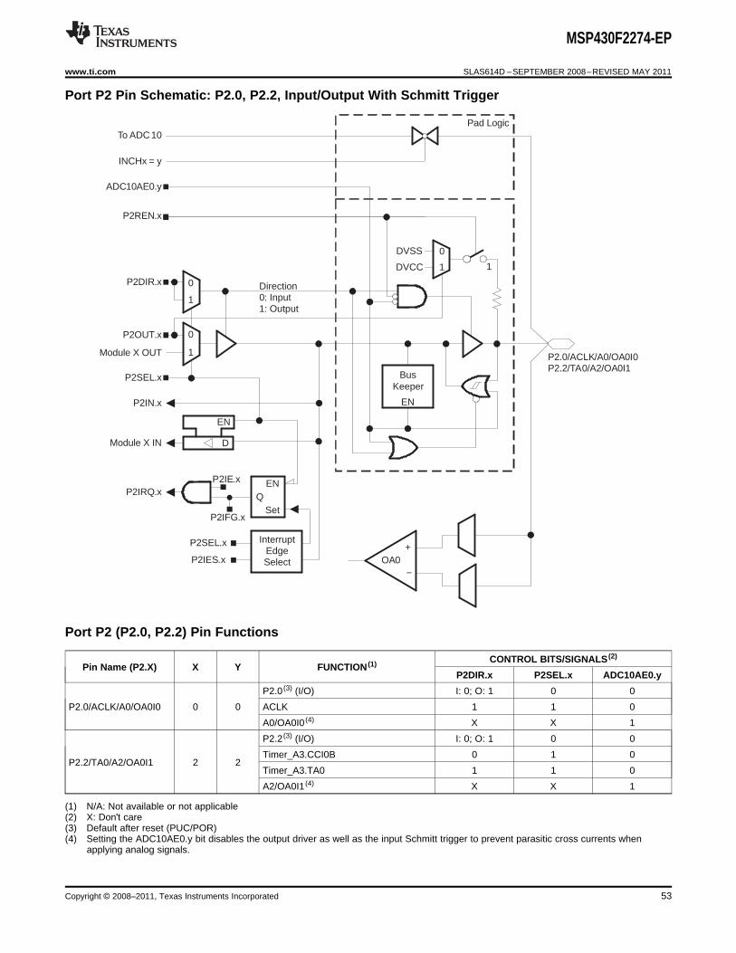
BusKeeper
EN
Direction0: Input1: Output
P2SEL.x
1
0P2DIR.x
P2IN.x
P2IRQ.x
D
EN
Module X IN
1
0
Module X OUT
P2OUT.x
InterruptEdgeSelect
QEN
Set
P2SEL.x
P2IES.x
P2IFG.x
P2IE.x
P2.0/ACLK/A0/OA0I0P2.2/TA0/A2/OA0I1
1
0DVSS
DVCC
P2REN.x
ADC10AE0.y
Pad Logic
INCHx = y
To ADC 10
1
OA0+
−
MSP430F2274-EP
www.ti.com SLAS614D –SEPTEMBER 2008–REVISED MAY 2011
Port P2 Pin Schematic: P2.0, P2.2, Input/Output With Schmitt Trigger
Port P2 (P2.0, P2.2) Pin Functions
CONTROL BITS/SIGNALS (2)
Pin Name (P2.X) X Y FUNCTION (1)
P2DIR.x P2SEL.x ADC10AE0.y
P2.0 (3) (I/O) I: 0; O: 1 0 0
P2.0/ACLK/A0/OA0I0 0 0 ACLK 1 1 0
A0/OA0I0 (4) X X 1
P2.2 (3) (I/O) I: 0; O: 1 0 0
Timer_A3.CCI0B 0 1 0P2.2/TA0/A2/OA0I1 2 2
Timer_A3.TA0 1 1 0
A2/OA0I1 (4) X X 1
(1) N/A: Not available or not applicable(2) X: Don't care(3) Default after reset (PUC/POR)(4) Setting the ADC10AE0.y bit disables the output driver as well as the input Schmitt trigger to prevent parasitic cross currents when
applying analog signals.
Copyright © 2008–2011, Texas Instruments Incorporated 53

1
OAFCxOAPMx
OAADCx
To OA0 Feedback Network1
(OAADCx = 10 or OAFCx = 000) and OAPMx > 00
BusKeeper
EN
Direction0: Input1: Output
P2SEL.1
1
0P2DIR.1
P2IN.1
P2IRQ.1
D
EN
Module X IN
1
0
Module X OUT
P2OUT.1
InterruptEdgeSelect
QEN
Set
P2SEL.1
P2IES.1
P2IFG.1
P2IE.1
P2.1/TAINCLK/SMCLK/A1/OA0O
1
0DVSS
DVCC
P2REN.1
ADC10AE0.1
Pad Logic
INCHx = 1
To ADC 10
1
OA0+
−
1
MSP430F2274-EP
SLAS614D –SEPTEMBER 2008–REVISED MAY 2011 www.ti.com
Port P2 Pin Schematic: P2.1, Input/Output With Schmitt Trigger
54 Copyright © 2008–2011, Texas Instruments Incorporated

BusKeeper
EN
Direction0: Input1: Output
P2SEL.3
1
0P2DIR.3
P2IN.3
P2IRQ.3
D
EN
Module X IN
1
0
Module X OUT
P2OUT.3
InterruptEdgeSelect
QEN
Set
P2SEL.3
P2IES.3
P2IFG.3
P2IE.3
1
0DVSS
DVCC
P2REN.3
ADC10AE0.3
Pad Logic
INCHx = 3
To ADC 10
1
OA1+
−
1
OAFCxOAPMx
OAADCx
To OA1 Feedback Network
To ADC 10 VR− 1
0
SREF2
VSS
P2.3/TA1/A3/VREF−/VeREF−/OA1I1/OA1O
1
(OAADCx = 10 or OAFCx = 000) and OAPMx > 00
MSP430F2274-EP
www.ti.com SLAS614D –SEPTEMBER 2008–REVISED MAY 2011
Port P2 Pin Schematic: P2.3, Input/Output With Schmitt Trigger
Copyright © 2008–2011, Texas Instruments Incorporated 55

MSP430F2274-EP
SLAS614D –SEPTEMBER 2008–REVISED MAY 2011 www.ti.com
Port P2 (P2.1) Pin Functions
CONTROL BITS/SIGNALS (2)
PIN NAME (P2.X) X Y FUNCTION (1)
P2DIR.x P2SEL.x ADC10AE0.y
P2.1 (3) (I/O) I: 0; O: 1 0 0
Timer_A3.INCLK 0 1 0P2.1/TAINCLK/SMCLK/A1/OA0O 1 1
SMCLK 1 1 0
A1/OA0O (4) X X 1
(1) N/A: Not available or not applicable(2) X: Don't care(3) Default after reset (PUC/POR)(4) Setting the ADC10AE0.y bit disables the output driver as well as the input Schmitt trigger to prevent parasitic cross currents when
applying analog signals.
Port P2 (P2.3) Pin Functions
CONTROL BITS/SIGNALS (2)
PIN NAME (P2.X) X Y FUNCTION (1)
P2DIR.x P2SEL.x ADC10AE0.y
P2.3 (3) (I/O) I: 0; O: 1 0 0
Timer_A3.CCI1B 0 1 0P2.3/TA1/A3/VREF–/VeREF–/OA1I1/OA1O 3 3
Timer_A3.TA1 1 1 0
A3/VREF–/VeREF–/OA1I1/OA1O (4) X X 1
(1) N/A: Not available or not applicable(2) X: Don't care(3) Default after reset (PUC/POR)(4) Setting the ADC10AE0.y bit disables the output driver as well as the input Schmitt trigger to prevent parasitic cross currents when
applying analog signals.
56 Copyright © 2008–2011, Texas Instruments Incorporated

BusKeeper
EN
Direction0: Input1: Output
P2SEL.4
1
0P2DIR.4
P2IN.4
P2IRQ.4
D
EN
Module X IN
1
0
Module X OUT
P2OUT.4
InterruptEdgeSelect
QEN
Set
P2SEL.4
P2IES.4
P2IFG.4
P2IE.4
P2.4/TA2/A4/VREF+/VeREF+/OA1I0
1
0DVSS
DVCC
P2REN.4
ADC10AE0.4
Pad Logic
INCHx = 4
To ADC 10
1
To/from ADC10positive reference
OA1+
−
MSP430F2274-EP
www.ti.com SLAS614D –SEPTEMBER 2008–REVISED MAY 2011
Port P2 Pin Schematic: P2.4, Input/Output With Schmitt Trigger
Port P2 (P2.4) Pin Functions
CONTROL BITS/SIGNALS (2)
PIN NAME (P2.X) X Y FUNCTION (1)
P2DIR.x P2SEL.x ADC10AE0.y
P2.4 (3) (I/O) I: 0; O: 1 0 0
P2.4/TA2/A4/VREF+/VeREF+/OA1I0 4 4 Timer_A3.TA2 1 1 0
A4/VREF+/VeREF+/OA1I0 (4) X X 1
(1) N/A: Not available or not applicable(2) X: Don't care(3) Default after reset (PUC/POR)(4) Setting the ADC10AE0.y bit disables the output driver as well as the input Schmitt trigger to prevent parasitic cross currents when
applying analog signals.
Copyright © 2008–2011, Texas Instruments Incorporated 57

BusKeeper
EN
Direction0: Input1: Output
P1SEL.x
1
0P1DIR.x
P1IN.x
P1IRQ.x
D
EN
Module X IN
1
0
Module X OUT
P1OUT.x
InterruptEdgeSelect
QEN
Set
P1SEL.x
P1IES.x
P1IFG.x
P1IE.x
P2.5/ROSC
1
0DVSS
DVCC
P1REN.x
DCOR
Pad LogicTo DCO
1
MSP430F2274-EP
SLAS614D –SEPTEMBER 2008–REVISED MAY 2011 www.ti.com
Port P2 Pin Schematic: P2.5, Input/Output With Schmitt Trigger and External ROSC for DCO
Port P2 (P2.5) Pin Functions
CONTROL BITS/SIGNALS (1)
PIN NAME (P2.X) X FUNCTIONP2DIR.x P2SEL.x DCOR
P2.5 (2) (I/O) 0/1 0 0
N/A (3) 0 1 0P2.5/ROSC 5
DVSS 1 1 0
ROSC X X 1
(1) X: Don't care(2) Default after reset (PUC/POR)(3) N/A: Not available or not applicable
58 Copyright © 2008–2011, Texas Instruments Incorporated

LFXT1 off
P2SEL.7
BusKeeper
EN
Direction0: Input1: Output
P2SEL.6
1
0P2DIR.6
P2IN.6
P2IRQ.6
D
EN
Module X IN
1
0
Module X OUT
P2OUT.6
InterruptEdgeSelect
QEN
Set
P2SEL.6
P2IES.6
P2IFG.6
P2IE.6
P2.6/XIN
1
0DVSS
DVCC
P2REN.6
Pad Logic
LFXT1 OscillatorBCSCTL3.LFXT1Sx = 11
P2.7/XOUT
0
1
1
LFXT1CLK
MSP430F2274-EP
www.ti.com SLAS614D –SEPTEMBER 2008–REVISED MAY 2011
Port P2 Pin Schematic: P2.6, Input/Output With Schmitt Trigger and Crystal Oscillator Input
Port P2 (P2.6) Pin Functions
CONTROL BITS/SIGNALS (2)
PIN NAME (P2.X) X FUNCTION (1)
P2DIR.x P2SEL.x
P2.6 (I/O) I: 0; O: 1 0P2.6/XIN 6
XIN (3) X 1
(1) N/A: Not available or not applicable(2) X: Don't care(3) Default after reset (PUC/POR)
Copyright © 2008–2011, Texas Instruments Incorporated 59

LFXT1 off
P2SEL.6
BusKeeper
EN
Direction0: Input1: Output
P2SEL.7
1
0P2DIR.7
P2IN.7
P2IRQ.7
D
EN
Module X IN
1
0
Module X OUT
P2OUT.7
InterruptEdgeSelect
QEN
Set
P2SEL.7
P2IES.7
P2IFG.7
P2IE.7
P2.7/XOUT
1
0DVSS
DVCC
P2REN.7
Pad Logic
LFXT1 OscillatorBCSCTL3.LFXT1Sx = 11
0
1
1
LFXT1CLK From P2.6/XIN P2.6/XIN
MSP430F2274-EP
SLAS614D –SEPTEMBER 2008–REVISED MAY 2011 www.ti.com
Port P2 Pin Schematic: P2.7, Input/Output With Schmitt Trigger and Crystal Oscillator Output
Port P2 (P2.7) Pin Functions
CONTROL BITS/SIGNALS (2)
PIN NAME (P2.X) X FUNCTION (1)
P2DIR.x P2SEL.x
P2.7 (I/O) I: 0; O: 1 0XOUT/P2.7 6
XOUT (3) (4) X 1
(1) N/A: Not available or not applicable(2) X: Don't care(3) Default after reset (PUC/POR)(4) If the pin XOUT/P2.7 is used as an input a current can flow until P2SEL.7 is cleared due to the oscillator output driver connection to this
pin after reset.
60 Copyright © 2008–2011, Texas Instruments Incorporated

BusKeeper
EN
Direction0: Input1: Output
P3SEL.0
1
0P3DIR.0
P3IN.0
D
EN
Module X IN
1
0
Module X OUT
P3OUT.0
P3.0/UC1STE/UC0CLK/A5
1
0DVSS
DVCC
P3REN.0
ADC10AE0.5
Pad Logic
INCHx = 5
To ADC10
1
USCI DirectionControl
MSP430F2274-EP
www.ti.com SLAS614D –SEPTEMBER 2008–REVISED MAY 2011
Port P3 Pin Schematic: P3.0, Input/Output With Schmitt Trigger
Port P3 (P3.0) Pin Functions
CONTROL BITS/SIGNALS (2)
PIN NAME (P1.X) X Y FUNCTION (1)
P3DIR.x P3SEL.x ADC10AE0.y
P3.0 (3) (I/O) I: 0; O: 1 0 0
P3.0/UC1STE/UC0CLK/A5 0 5 UC1STE/UC0CLK (4) (5) X 1 0
A5 (6) X X 1
(1) N/A: Not available or not applicable(2) X: Don't care(3) Default after reset (PUC/POR)(4) The pin direction is controlled by the USCI module.(5) UC0CLK function takes precedence over UC1STE function. If the pin is required as UC0CLK input or output USCI1 is forced to 3-wire
SPI mode if 4-wire SPI mode is selected.(6) Setting the ADC10AE0.y bit disables the output driver as well as the input Schmitt trigger to prevent parasitic cross currents when
applying analog signals.
Copyright © 2008–2011, Texas Instruments Incorporated 61

BusKeeper
EN
Direction0: Input1: Output
P3SEL.x
1
0P3DIR.x
P3IN.x
D
EN
Module X IN
1
0
Module X OUT
P3OUT.x
P3.1/UC1SIMO/UC1SCLP3.2/UC1SOMI/UC1SDAP3.3/UC1CLK/UC0STEP3.4/UC0TXD/UC0SIMOP3.5/UC0RXD/UC0SOMI
1
0DVSS
DVCC
P3REN.x
Pad Logic
1
USCI DirectionControl
DVSS
MSP430F2274-EP
SLAS614D –SEPTEMBER 2008–REVISED MAY 2011 www.ti.com
Port P3 Pin Schematic: P3.1 to P3.5, Input/Output With Schmitt Trigger
Port P3 (P3.1 to P3.5) Pin Functions
CONTROL BITS/SIGNALS (2)
PIN NAME (P3.X) X FUNCTION (1)
P3DIR.x P3SEL.x
P3.1 (3) (I/O) I: 0; O: 1 0P3.1/UC1SIMO/UC1SDA 1
UC1SIMO/UC1SDA (4) X 1
P3.2 (5) (I/O) I: 0; O: 1 0P3.2/UC1SOMI/UC1SCL 1
UC1SOMI/UC1SCL (6) X 1
P3.3 (5) (I/O) I: 0; O: 1 0P3.3/UC1CLK/UC0STE 1
UC1CLK/UC0STE (6) (7) X 1
P3.4 (5) (I/O) I: 0; O: 1 0P3.4/UC0TXD/UC0SIMO 1
UC0TXD/UC0SIMO (6) X 1
P3.5 (5) (I/O) I: 0; O: 1 0P3.5/UC0RXD/UC0SOMI 1
UC0RXD/UC0SOMI (6) X 1
(1) N/A: Not available or not applicable(2) X: Don't care(3) Default after reset (PUC/POR)(4) The pin direction is controlled by the USCI module.(5) Default after reset (PUC/POR)(6) The pin direction is controlled by the USCI module.(7) UC1CLK function takes precedence over UC0STE function. If the pin is required as UC1CLK input or output, USCI0 is orced to 3-wire
SPI mode even if 4-wire SPI mode is selected.
62 Copyright © 2008–2011, Texas Instruments Incorporated

BusKeeper
EN
Direction0: Input1: Output
P3SEL.x
1
0P3DIR.x
P3IN.x
D
EN
Module X IN
1
0
Module X OUT
P3OUT.x
P3.6/A6/OA0I2P3.7/A7/OA1I2
1
0DVSS
DVCC
P3REN.x
ADC10AE0.y
Pad Logic
INCHx = y
To ADC 10
1
OA0/1+
−
MSP430F2274-EP
www.ti.com SLAS614D –SEPTEMBER 2008–REVISED MAY 2011
Port P3 Pin Schematic: P3.6 to P3.7, Input/Output With Schmitt Trigger
Port P3 (P3.6, P3.7) Pin Functions
CONTROL BITS/SIGNALS (3)
PIN NAME (P3.X) X Y FUNCTION (1) (2)
P3DIR.x P3SEL.x ADC10AE0.y
P3.6 (4) (I/O) I: 0; O: 1 0 0P3.6/A6/OA0I2 6 6
A6/OA0I2 (5) X X 1
P3.7 (4) (I/O) I: 0; O: 1 0 0P3.7/A7/OA1I2 7 7
A7/OA1I2 (5) X X 1
(1) N/A: Not available or not applicable(2) UC0CLK function takes precedence over UC0STE function. If the pin is required as UC1CLK input or output, USCI0 is forced to 3-wire
SPI mode if 4-wire SPI mode is selected.(3) X: Don't care(4) Default after reset (PUC/POR)(5) Setting the ADC10AE0.y bit disables the output driver as well as the input Schmitt trigger to prevent parasitic cross currents when
applying analog signals.
Copyright © 2008–2011, Texas Instruments Incorporated 63

BusKeeper
EN
Direction0: Input1: Output
P4SEL.x
1
0P4DIR.x
P4IN.x
D
EN
Module X IN
1
0
Module X OUT
P4OUT.x
P4.0/TB0P4.1/TB1P4.2/TB2
1
0DVSS
DVCC
P4REN.x
Pad Logic
1
P4DIR.6P4SEL.6
ADC10AE1.7
P4.6/TBOUTH/A15/OA1I3
Timer_B Output Tristate Logic
MSP430F2274-EP
SLAS614D –SEPTEMBER 2008–REVISED MAY 2011 www.ti.com
Port P4 Pin Schematic: P4.0 to P4.2, Input/Output With Schmitt Trigger
Port P4 (P4.0 to P4.2) Pin Functions
CONTROL BITS/SIGNALSPIN NAME (P4.X) X FUNCTION (1)
P4DIR.x P4SEL.x
P4.0 (2) (I/O) I: 0; O: 1 0
P4.0/TB0 0 Timer_B3.CCI0A 0 1
Timer_B3.TB0 1 1
P4.1 (2) (I/O) I: 0; O: 1 0
P4.1/TB1 1 Timer_B3.CCI1A 0 1
Timer_B3.TB1 1 1
P4.2 (2) (I/O) I: 0; O: 1 0
P4.2/TB2 2 Timer_B3.CCI2A 0 1
Timer_B3.TB2 1 1
(1) N/A: Not available or not applicable.(2) Default after reset (PUC/POR)
64 Copyright © 2008–2011, Texas Instruments Incorporated
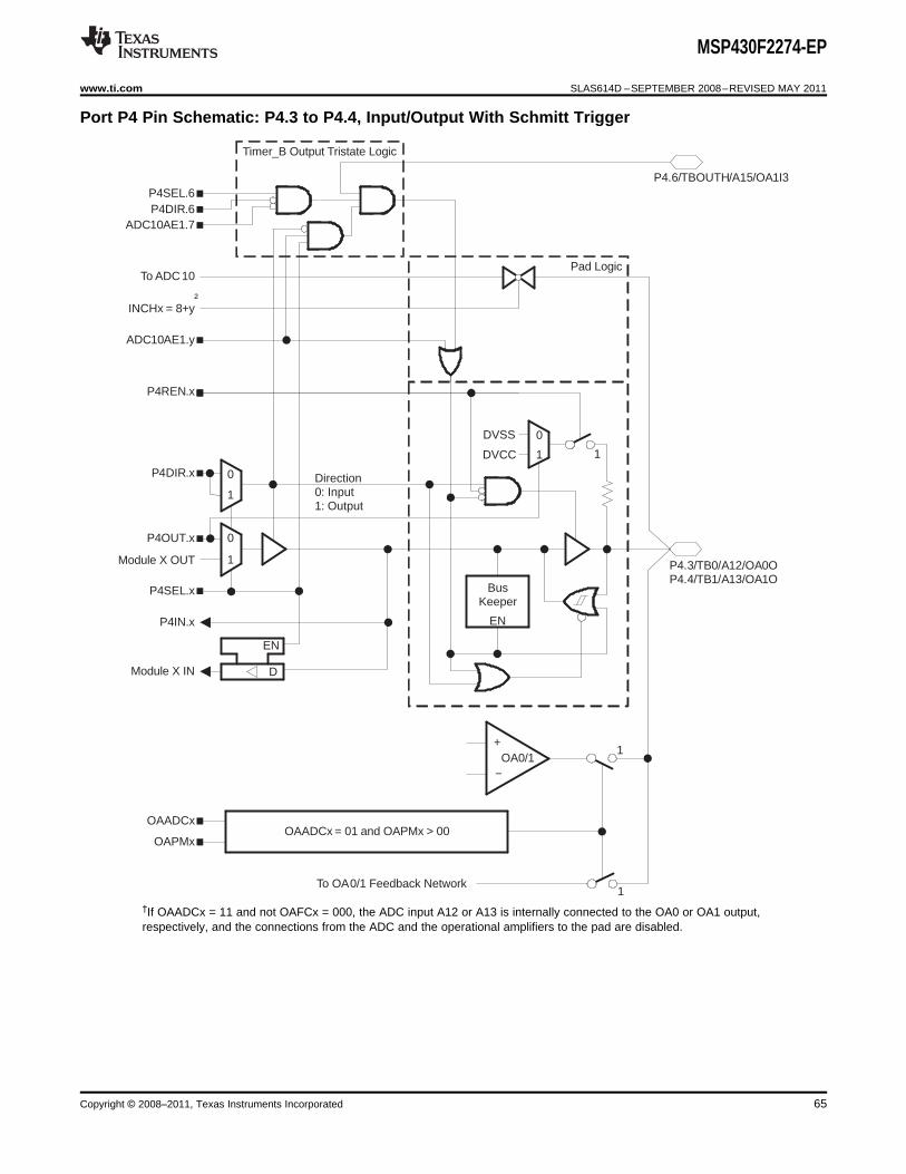
OAPMx
OAADCx
To OA0/1 Feedback Network1
OAADCx = 01 and OAPMx > 00
BusKeeper
EN
Direction0: Input1: Output
P4SEL.x
1
0P4DIR.x
P4IN.x
D
EN
Module X IN
1
0
Module X OUT
P4OUT.x
P4.3/TB0/A12/OA0OP4.4/TB1/A13/OA1O
1
0DVSS
DVCC
P4REN.x
ADC10AE1.y
Pad Logic
INCHx = 8+y
To ADC 10
1
OA0/1+
−
1
P4DIR.6P4SEL.6
ADC10AE1.7
P4.6/TBOUTH/A15/OA1I3
Timer_B Output Tristate Logic
†
MSP430F2274-EP
www.ti.com SLAS614D –SEPTEMBER 2008–REVISED MAY 2011
Port P4 Pin Schematic: P4.3 to P4.4, Input/Output With Schmitt Trigger
†If OAADCx = 11 and not OAFCx = 000, the ADC input A12 or A13 is internally connected to the OA0 or OA1 output,respectively, and the connections from the ADC and the operational amplifiers to the pad are disabled.
Copyright © 2008–2011, Texas Instruments Incorporated 65

MSP430F2274-EP
SLAS614D –SEPTEMBER 2008–REVISED MAY 2011 www.ti.com
Port P4 (P4.3 to P4.4) Pin Functions
CONTROL BITS/SIGNALS (2)
PIN NAME (P4.X) X Y FUNCTION (1)
P4DIR.x P4SEL.x ADC10AE1.y
P4.3 (3) (I/O) I: 0; O: 1 0 0
Timer_B3.CCI0B 0 1 0P4.3/TB0/A12/OA0O 3 4
Timer_B3.TB0 1 1 0
A12/OA0O (4) X X 1
P4.4 (3) (I/O) I: 0; O: 1 0 0
Timer_B3.CCI1B 0 1 0P4.4/TB1/A13/OA1O 4 5
Timer_B3.TB1 1 1 0
A13/OA1O (4) X X 1
(1) N/A: Not available or not applicable(2) X: Don't care(3) Default after reset (PUC/POR)(4) Setting the ADC10AE1.y bit disables the output driver as well as the input Schmitt trigger to prevent parasitic cross currents when
applying analog signals.
66 Copyright © 2008–2011, Texas Instruments Incorporated

BusKeeper
EN
Direction0: Input1: Output
P4SEL.5
1
0P4DIR.5
P4IN.5
D
EN
Module X IN
1
0
Module X OUT
P4OUT.5
P4.5/TB3/A14/OA0I3
1
0DVSS
DVCC
P4REN.5
ADC10AE1.6
Pad Logic
INCHx = 14
To ADC 10
1
P4DIR.6P4SEL.6
ADC10AE1.7
P4.6/TBOUTH/A15/OA1I3
Timer_B Output Tristate Logic
OA0+
−
MSP430F2274-EP
www.ti.com SLAS614D –SEPTEMBER 2008–REVISED MAY 2011
Port P4 Pin Schematic: P4.5, Input/Output With Schmitt Trigger
Port P4 (P4.5) Pin Functions
CONTROL BITS/SIGNALS (2)
PIN NAME (P4.X) X Y FUNCTION (1)
P4DIR.x P4SEL.x ADC10AE1.y
P4.5 (3) (I/O) I: 0; O: 1 0 0
P4.5/TB3/A14/OA0I3 5 6 Timer_B3.TB2 1 1 0
A14/OA0I3 (4) X X 1
(1) N/A: Not available or not applicable(2) X: Don't care(3) Default after reset (PUC/POR)(4) Setting the ADC10AE1.y bit disables the output driver as well as the input Schmitt trigger to prevent parasitic cross currents when
applying analog signals.
Copyright © 2008–2011, Texas Instruments Incorporated 67

BusKeeper
EN
Direction0: Input1: Output
P4SEL.6
1
0P4DIR.6
P4IN.6
D
EN
Module X IN
1
0
Module X OUT
P4OUT.6
1
0DVSS
DVCC
P4REN.6
ADC10AE1.7
Pad Logic
INCHx = 15
To ADC 10
1
OA1+
−
P4.6/TBOUTH/A15/OA1I3
MSP430F2274-EP
SLAS614D –SEPTEMBER 2008–REVISED MAY 2011 www.ti.com
Port P4 Pin Schematic: P4.6, Input/Output With Schmitt Trigger
Port P4 (P4.6) Pin Functions
CONTROL BITS/SIGNALS (2)
PIN NAME (P4.X) X Y FUNCTION (1)
P4DIR.x P4SEL.x ADC10AE1.y
P4.6 (3) (I/O) I: 0; O: 1 0 0
TBOUTH 0 1 0P4.6/TBOUTH/A15/OA1I3 6 7
DVSS 1 1 0
A15/OA1I3 (4) X X 1
(1) N/A: Not available or not applicable(2) X: Don't care(3) Default after reset (PUC/POR)(4) Setting the ADC10AE1.y bit disables the output driver as well as the input Schmitt trigger to prevent parasitic cross currents when
applying analog signals.
68 Copyright © 2008–2011, Texas Instruments Incorporated

BusKeeper
EN
Direction0: Input1: Output
P4SEL.x
1
0P4DIR.x
P4IN.x
D
EN
Module X IN
1
0
Module X OUT
P4OUT.x
P4.7/TBCLK
1
0DVSS
DVCC
P4REN.x
Pad Logic
1
DVSS
MSP430F2274-EP
www.ti.com SLAS614D –SEPTEMBER 2008–REVISED MAY 2011
Port P4 Pin Schematic: P4.7, Input/Output With Schmitt Trigger
Port P4 (Pr.7) Pin Functions
CONTROL BITS/SIGNALSPIN NAME (P4.X) X FUNCTION (1)
P4DIR.x P4SEL.x
P4.7 (2) (I/O) I: 0; O: 1 0
P4.7/TBCLK 7 Timer_B3.TBCLK 0 1
DVSS 1 1
(1) N/A: Not available or not applicable(2) Default after reset (PUC/POR)
Copyright © 2008–2011, Texas Instruments Incorporated 69

Time TMS Goes Low After POR
TMS
ITFITEST
MSP430F2274-EP
SLAS614D –SEPTEMBER 2008–REVISED MAY 2011 www.ti.com
JTAG Fuse Check Mode
MSP430 devices that have the fuse on the TEST terminal have a fuse check mode that tests the continuity of thefuse the first time the JTAG port is accessed after a power-on reset (POR). When activated, a fuse checkcurrent, ITF , of 1 mA at 3 V, 2.5 mA at 5 V can flow from the TEST pin to ground if the fuse is not burned. Caremust be taken to avoid accidentally activating the fuse check mode and increasing overall system powerconsumption.
When the TEST pin is again taken low after a test or programming session, the fuse check mode and sensecurrents are terminated.
Activation of the fuse check mode occurs with the first negative edge on the TMS pin after power up or if TMS isbeing held low during power up. The second positive edge on the TMS pin deactivates the fuse check mode.After deactivation, the fuse check mode remains inactive until another POR occurs. After each POR the fusecheck mode has the potential to be activated.
The fuse check current flows only when the fuse check mode is active and the TMS pin is in a low state (seeFigure 28). Therefore, the additional current flow can be prevented by holding the TMS pin high (defaultcondition).
Figure 28. Fuse Check Mode Current, MSP430F22xx
NOTEThe CODE and RAM data protection is ensured if the JTAG fuse is blown and the 256-bitbootloader access key is used. Also, see the Bootstrap Loader section for moreinformation.
70 Copyright © 2008–2011, Texas Instruments Incorporated

PACKAGE OPTION ADDENDUM
www.ti.com 1-Dec-2012
Addendum-Page 1
PACKAGING INFORMATION
Orderable Device Status(1)
Package Type PackageDrawing
Pins Package Qty Eco Plan(2)
Lead/Ball Finish MSL Peak Temp(3)
Samples(Requires Login)
MSP430F2274MDATEP ACTIVE TSSOP DA 38 250 Green (RoHS& no Sb/Br)
CU NIPDAU Level-2-260C-1 YEAR
MSP430F2274MRHATEP ACTIVE VQFN RHA 40 250 Green (RoHS& no Sb/Br)
CU NIPDAU Level-3-260C-168 HR
V62/08631-01XE ACTIVE VQFN RHA 40 250 Green (RoHS& no Sb/Br)
CU NIPDAU Level-3-260C-168 HR
V62/08631-01YE ACTIVE TSSOP DA 38 250 Green (RoHS& no Sb/Br)
CU NIPDAU Level-2-260C-1 YEAR
(1) The marketing status values are defined as follows:ACTIVE: Product device recommended for new designs.LIFEBUY: TI has announced that the device will be discontinued, and a lifetime-buy period is in effect.NRND: Not recommended for new designs. Device is in production to support existing customers, but TI does not recommend using this part in a new design.PREVIEW: Device has been announced but is not in production. Samples may or may not be available.OBSOLETE: TI has discontinued the production of the device.
(2) Eco Plan - The planned eco-friendly classification: Pb-Free (RoHS), Pb-Free (RoHS Exempt), or Green (RoHS & no Sb/Br) - please check http://www.ti.com/productcontent for the latest availabilityinformation and additional product content details.TBD: The Pb-Free/Green conversion plan has not been defined.Pb-Free (RoHS): TI's terms "Lead-Free" or "Pb-Free" mean semiconductor products that are compatible with the current RoHS requirements for all 6 substances, including the requirement thatlead not exceed 0.1% by weight in homogeneous materials. Where designed to be soldered at high temperatures, TI Pb-Free products are suitable for use in specified lead-free processes.Pb-Free (RoHS Exempt): This component has a RoHS exemption for either 1) lead-based flip-chip solder bumps used between the die and package, or 2) lead-based die adhesive used betweenthe die and leadframe. The component is otherwise considered Pb-Free (RoHS compatible) as defined above.Green (RoHS & no Sb/Br): TI defines "Green" to mean Pb-Free (RoHS compatible), and free of Bromine (Br) and Antimony (Sb) based flame retardants (Br or Sb do not exceed 0.1% by weightin homogeneous material)
(3) MSL, Peak Temp. -- The Moisture Sensitivity Level rating according to the JEDEC industry standard classifications, and peak solder temperature.
Important Information and Disclaimer:The information provided on this page represents TI's knowledge and belief as of the date that it is provided. TI bases its knowledge and belief on informationprovided by third parties, and makes no representation or warranty as to the accuracy of such information. Efforts are underway to better integrate information from third parties. TI has taken andcontinues to take reasonable steps to provide representative and accurate information but may not have conducted destructive testing or chemical analysis on incoming materials and chemicals.TI and TI suppliers consider certain information to be proprietary, and thus CAS numbers and other limited information may not be available for release.
In no event shall TI's liability arising out of such information exceed the total purchase price of the TI part(s) at issue in this document sold by TI to Customer on an annual basis.
OTHER QUALIFIED VERSIONS OF MSP430F2274-EP :

PACKAGE OPTION ADDENDUM
www.ti.com 1-Dec-2012
Addendum-Page 2
• Catalog: MSP430F2274
• Automotive: MSP430F2274-Q1
NOTE: Qualified Version Definitions:
• Catalog - TI's standard catalog product
• Automotive - Q100 devices qualified for high-reliability automotive applications targeting zero defects

TAPE AND REEL INFORMATION
*All dimensions are nominal
Device PackageType
PackageDrawing
Pins SPQ ReelDiameter
(mm)
ReelWidth
W1 (mm)
A0(mm)
B0(mm)
K0(mm)
P1(mm)
W(mm)
Pin1Quadrant
MSP430F2274MRHATEP VQFN RHA 40 250 180.0 16.4 6.3 6.3 1.1 12.0 16.0 Q2
PACKAGE MATERIALS INFORMATION
www.ti.com 17-Dec-2011
Pack Materials-Page 1

*All dimensions are nominal
Device Package Type Package Drawing Pins SPQ Length (mm) Width (mm) Height (mm)
MSP430F2274MRHATEP VQFN RHA 40 250 210.0 185.0 35.0
PACKAGE MATERIALS INFORMATION
www.ti.com 17-Dec-2011
Pack Materials-Page 2


IMPORTANT NOTICE
Texas Instruments Incorporated and its subsidiaries (TI) reserve the right to make corrections, enhancements, improvements and otherchanges to its semiconductor products and services per JESD46, latest issue, and to discontinue any product or service per JESD48, latestissue. Buyers should obtain the latest relevant information before placing orders and should verify that such information is current andcomplete. All semiconductor products (also referred to herein as “components”) are sold subject to TI’s terms and conditions of salesupplied at the time of order acknowledgment.
TI warrants performance of its components to the specifications applicable at the time of sale, in accordance with the warranty in TI’s termsand conditions of sale of semiconductor products. Testing and other quality control techniques are used to the extent TI deems necessaryto support this warranty. Except where mandated by applicable law, testing of all parameters of each component is not necessarilyperformed.
TI assumes no liability for applications assistance or the design of Buyers’ products. Buyers are responsible for their products andapplications using TI components. To minimize the risks associated with Buyers’ products and applications, Buyers should provideadequate design and operating safeguards.
TI does not warrant or represent that any license, either express or implied, is granted under any patent right, copyright, mask work right, orother intellectual property right relating to any combination, machine, or process in which TI components or services are used. Informationpublished by TI regarding third-party products or services does not constitute a license to use such products or services or a warranty orendorsement thereof. Use of such information may require a license from a third party under the patents or other intellectual property of thethird party, or a license from TI under the patents or other intellectual property of TI.
Reproduction of significant portions of TI information in TI data books or data sheets is permissible only if reproduction is without alterationand is accompanied by all associated warranties, conditions, limitations, and notices. TI is not responsible or liable for such altereddocumentation. Information of third parties may be subject to additional restrictions.
Resale of TI components or services with statements different from or beyond the parameters stated by TI for that component or servicevoids all express and any implied warranties for the associated TI component or service and is an unfair and deceptive business practice.TI is not responsible or liable for any such statements.
Buyer acknowledges and agrees that it is solely responsible for compliance with all legal, regulatory and safety-related requirementsconcerning its products, and any use of TI components in its applications, notwithstanding any applications-related information or supportthat may be provided by TI. Buyer represents and agrees that it has all the necessary expertise to create and implement safeguards whichanticipate dangerous consequences of failures, monitor failures and their consequences, lessen the likelihood of failures that might causeharm and take appropriate remedial actions. Buyer will fully indemnify TI and its representatives against any damages arising out of the useof any TI components in safety-critical applications.
In some cases, TI components may be promoted specifically to facilitate safety-related applications. With such components, TI’s goal is tohelp enable customers to design and create their own end-product solutions that meet applicable functional safety standards andrequirements. Nonetheless, such components are subject to these terms.
No TI components are authorized for use in FDA Class III (or similar life-critical medical equipment) unless authorized officers of the partieshave executed a special agreement specifically governing such use.
Only those TI components which TI has specifically designated as military grade or “enhanced plastic” are designed and intended for use inmilitary/aerospace applications or environments. Buyer acknowledges and agrees that any military or aerospace use of TI componentswhich have not been so designated is solely at the Buyer's risk, and that Buyer is solely responsible for compliance with all legal andregulatory requirements in connection with such use.
TI has specifically designated certain components as meeting ISO/TS16949 requirements, mainly for automotive use. In any case of use ofnon-designated products, TI will not be responsible for any failure to meet ISO/TS16949.
Products Applications
Audio www.ti.com/audio Automotive and Transportation www.ti.com/automotive
Amplifiers amplifier.ti.com Communications and Telecom www.ti.com/communications
Data Converters dataconverter.ti.com Computers and Peripherals www.ti.com/computers
DLP® Products www.dlp.com Consumer Electronics www.ti.com/consumer-apps
DSP dsp.ti.com Energy and Lighting www.ti.com/energy
Clocks and Timers www.ti.com/clocks Industrial www.ti.com/industrial
Interface interface.ti.com Medical www.ti.com/medical
Logic logic.ti.com Security www.ti.com/security
Power Mgmt power.ti.com Space, Avionics and Defense www.ti.com/space-avionics-defense
Microcontrollers microcontroller.ti.com Video and Imaging www.ti.com/video
RFID www.ti-rfid.com
OMAP Applications Processors www.ti.com/omap TI E2E Community e2e.ti.com
Wireless Connectivity www.ti.com/wirelessconnectivity
Mailing Address: Texas Instruments, Post Office Box 655303, Dallas, Texas 75265Copyright © 2012, Texas Instruments Incorporated