m.s.engineering college, navarathna … · hdl lab manual iv sem ec dept of e&c 1 m.s....
TRANSCRIPT

HDL Lab Manual IV Sem EC
Dept of E&C 1 M.S. Engineering College, Bangalore
M.S.ENGINEERING COLLEGE,
NAVARATHNA AGRAHARA ,SADAHALLI
POST,
BANGALORE-562110.
Dept of
ELECTRONICS AND COMMUNICATION
ENGINEERING
SUB : HDL LAB MANUAL
CODE : 06ECL48
Prepared By: Sunitha P.H , Associate Professor
&
Vinod kumar BL, Assistant professor

HDL Lab Manual IV Sem EC
Dept of E&C 2 M.S. Engineering College, Bangalore
HDL lab manual
Software Experiments:
Experiment No 1:- Write and simulate the HDL code to realize all the logic gates.
Objective: - To write and simulate the HDL code to realize the basic logic gates and to check the
functionality by simulating the design using Mentor graphics Modelsim Simulator.
Theory: -
Z
1. AND
2. OR
3. XOR
4. NOT
5. NAND
6. NOR
7. XNOR
Any complex design has to be checked using these basic gates. Functionality of any
design can be realized using two gates called Universal gates namely
NAND
NOR
Functionality of all the logic gates can be best explained using the Functional table.
1.a) Realizing AND gate:
Program: in VHDL
--VHDL model for an AND gate
library ieee;
use ieee.std_logic_1164.all;
use ieee.std_logic_arith.all;
use ieee.std_logic_unsigned.all;
--entity of an AND gate begins
entity and1 is
port (a : in std_logic;
b : in std_logic;
c : out std_logic
);
end and1;

HDL Lab Manual IV Sem EC
Dept of E&C 3 M.S. Engineering College, Bangalore
--architecture of an AND gate begins
architecture behavioral of and1 is
begin
c<=a and b;
end behavioral;
Program: in Verilog
module and_gate (a,b,y);
input a,b ; //defines two input port
output y; // defines one output port
and g1(y,a,b); /*gate declaration with predefined keyword or representing
logic OR, g1 is optional user defined gate identifier */
endmodule
Functional table:
Input
A
Input
B
Output
Y
0 0 0
0 1 0
1 0 0
1 1 1
Simulation Results:-
1.b) Realizing OR gate:
Program: in VHDL

HDL Lab Manual IV Sem EC
Dept of E&C 4 M.S. Engineering College, Bangalore
library ieee;
use ieee.std_logic_1164.all;
use ieee.std_logic_arith.all;
use ieee.std_logic_unsigned.all;
--entity of an OR gate begins
entity or1 is
port ( a : in std_logic;
b : in std_logic;
c : out std_logic
);
end or1;
--architecture of an OR gate begins
architecture behavioral of or1 is
begin
c<=a or b;
end behavioral;
Program: in Verilog
//Verilog module for OR gate
module or_gate(a,b,y);
input a,b; //defines two input port
output y; // defines one output port
or g1(y,a,b); /*gate declaration with predefined keyword or representing
logic OR, g1 is optional user defined gate identifier */
endmodule
Functional table:
Input
A
Input
B
Output
Y
0 0 0
0 1 1
1 0 1
1 1 1
Simulation Results:-

HDL Lab Manual IV Sem EC
Dept of E&C 5 M.S. Engineering College, Bangalore
1.c).
Realizing
XOR gate:
Program:
in VHDL
library
IEEE;
use
IEEE.STD_
LOGIC_11
64.ALL;
use
IEEE.STD_
LOGIC_A
RITH.ALL;
use IEEE.STD_LOGIC_UNSIGNED.ALL;
entity xor1 is
port ( a : in std_logic;
b : in std_logic;
c : out std_logic
);
end xor1;
--architecture of an XOR gate begins
architecture behavioral of xor1 is
begin
c<=a xor b;
end behavioral;
Program: in Verilog:-
module xor_gate(y,a,b);
input a,b;
output y;
xor g1(y,a,b);
endmodule
Functional table:
Input
a
Input
b
Output
c
0 0 0
0 1 1
1 0 1
1 1 0

HDL Lab Manual IV Sem EC
Dept of E&C 6 M.S. Engineering College, Bangalore
Simulation Results
1.d)NOT GATE:
VHDL module for NOT gate
library IEEE;
use IEEE.STD_LOGIC_1164.ALL;
use IEEE.STD_LOGIC_ARITH.ALL;
use IEEE.STD_LOGIC_UNSIGNED.ALL;
entity not1 is
port ( a : in std_logic;
c : out std_logic
);
end not1;
architecture behavioral of not1 is
begin
c<=not a ;
end behavioral;
Verilog module for NOT gate module not_gate(a,y);
input a;
output y;
not g1(y,a);
endmodule
Functional table:
Input
A
Output
c
0 1
1 0
Simulation Results

HDL Lab Manual IV Sem EC
Dept of E&C 7 M.S. Engineering College, Bangalore
1. e) NAND GATE:
library IEEE;
use IEEE.STD_LOGIC_1164.ALL;
use IEEE.STD_LOGIC_ARITH.ALL;
use IEEE.STD_LOGIC_UNSIGNED.ALL;
entity nand1 is
port ( a : in std_logic;
b : in std_logic;
c : out std_logic
);
end nand1;
architecture behavioral of nand1 is
begin
c<=a xnor b;
end behavioral;
Verilog module for NAND gate
module nand_gate(a,b,y);
input a,b;
output y;
nand g1(y,a,b);
endmodule
Functional table:
Input Input Output
HDL Lab Manual IV Sem EC
Dept of E&C 8 M.S. Engineering College, Bangalore
A B c
0 0 1
0 1 1
1 0 1
1 1 0
Simulation Results
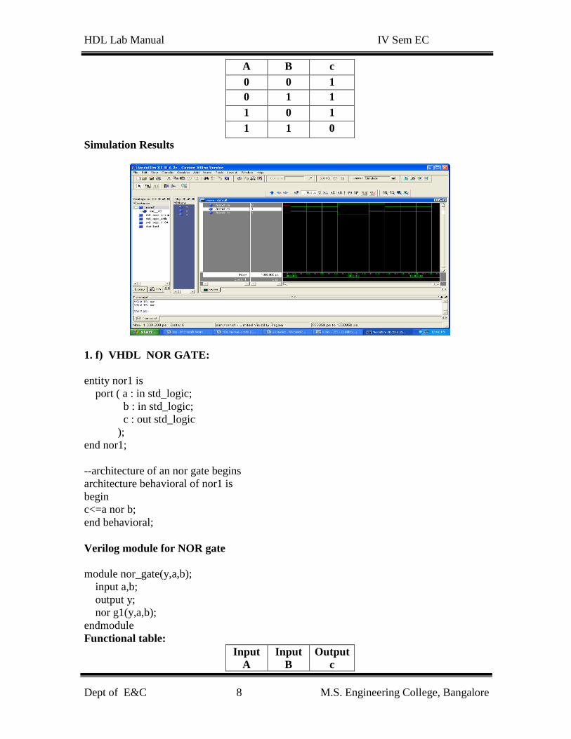
1. f) VHDL NOR GATE:
entity nor1 is
port ( a : in std_logic;
b : in std_logic;
c : out std_logic
);
end nor1;
--architecture of an nor gate begins
architecture behavioral of nor1 is
begin
c<=a nor b;
end behavioral;
Verilog module for NOR gate
module nor_gate(y,a,b);
input a,b;
output y;
nor g1(y,a,b);
endmodule
Functional table:
Input
A
Input
B
Output
c

HDL Lab Manual IV Sem EC
Dept of E&C 9 M.S. Engineering College, Bangalore
0 0 0
0 1 0
1 0 0
1 1 1
Simulation Results
1.g) VHDL program for XNOR:
library IEEE;
use IEEE.STD_LOGIC_1164.ALL;
use IEEE.STD_LOGIC_ARITH.ALL;
use IEEE.STD_LOGIC_UNSIGNED.ALL;
entity xnor1 is
port ( a : in std_logic;
b : in std_logic;
c : out std_logic
);
end xnor1;
architecture behavioral of xnor1 is
begin
c<=a xnor b;
end behavioral;
Verilog module for XNOR gate
module xnor_gate(y,a,b);
input a,b;
output y;
xnor g1(y,a,b);

HDL Lab Manual IV Sem EC
Dept of E&C 10 M.S. Engineering College, Bangalore
endmodule
Functional table:
Input
A
Input
B
Output
c
0 0 1
0 1 0
1 0 0
1 1 1
Simulation Results
Result:-
Written and simulated the HDL model for Basic logic gates and verified the
response with the truth table and concluded that the basic logic gates design is
working fine.
Experiment No 2:
Write and simulate the HDL designs for the following combinational circuits
2 to 4 decoder.
8 to 3 encoder without priority &
8 to 3 encoder with priority) .
8 to 1 Mux.
4 bit binary to gray converter .
Multiplexer, De-Multiplexer, Comparator
Objective: - To write and simulate the HDL code to realize the Combinational gates and to
check the functionality by simulating the design using Mentor graphics Modelsim
Simulator.
Theory: b) 2 to 4 decoder:
A decoder is a multiple input, multiple output logic circuit that converts coded inputs
into coded outputs where the input and output codes are different. The enable inputs

HDL Lab Manual IV Sem EC
Dept of E&C 11 M.S. Engineering College, Bangalore
must be ON for the decoder to function, otherwise its outputs assumes a ‘disabled’
output code word. Decoding is necessary in applications such as data multiplexing,
seven segment display and memory address decoding.
--VHDL model for 2:4 DECODER using when else statement
use ieee.std_logic_1164.all;
use ieee.std_logic_arith.all;
use ieee.std_logic_unsigned.all;
--entity of decoder begins
entity decoder6 is
port ( a : in std_logic_vector(1 downto 0);
y : out std_logic_vector(3 downto 0)
);
end decoder6;
--architecture of decoder begins
architecture behavioral of decoder6 is
begin
y<="1110" when a="00"else
"1101" when a="01" else
"1011" when a="10" else
"0111";
end behavioral;
//Verilog model for 2:4 DECODER using case statement
module decoder(a, y);
input [1:0] a;
output [3:0] y;
reg [3:0] y;
always @ (a)
case(a)
2‟b00: y<= 4‟b1110;
2‟b01: y<= 4‟b1101;
2‟b10: y<= 4‟b1011;
2‟b11: y<= 4‟b0111;
end case;
endmodule
2:4 Decoder a(0)
a(1)
y(2)
y(1)
y(0)
y(3)

HDL Lab Manual IV Sem EC
Dept of E&C 12 M.S. Engineering College, Bangalore
Functional table:
Input : a
(1downto 0)
Output :
y(1downto 0)
00 1110
01 1101
10 1011
11 0111
Simulation Results:-
Theory: b) 8 to 3 encoder:
(b.1) 8 to 3 encoder without priority
library IEEE;
use IEEE.STD_LOGIC_1164.ALL;
use IEEE.STD_LOGIC_ARITH.ALL;
use IEEE.STD_LOGIC_UNSIGNED.ALL;
entity enc83 is
port(e:in std_logic;
din: in std_logic_vector(7 downto 0);

HDL Lab Manual IV Sem EC
Dept of E&C 13 M.S. Engineering College, Bangalore
dout: out std_logic_vector(2 downto 0) );
end enc83;
architecture behavioral of enc83 is
begin
process(e ,din)
begin
if e='1' then
dout<="ZZZ";
else
case din is
when"00000001"=>dout<="000";
when"00000010"=>dout<="001";
when"00000100"=>dout<="010";
when"00001000"=>dout<="011";
when"00010000"=>dout<="100";
when"00100000"=>dout<="101";
when"01000000"=>dout<="110";
when others=>dout<="111";
end case;
end if;
end process;
end behavioral;
Verilog Code for 8 to 3 encoder without priority
module encoder (din, dout);
input [7:0] din;
output [2:0] dout;
reg [2:0] dout;
always @(din)
begin
if (din ==8'b00000001) dout=3'b000;
else if (din==8'b00000010) dout=3'b001;
else if (din==8'b00000100) dout=3'b010;
else if (din==8'b00001000) dout=3'b011;
else if (din==8'b00010000) dout=3'b100;
else if (din ==8'b00100000) dout=3'b101;
else if (din==8'b01000000) dout=3'b110;
else if (din==8'b10000000) dout=3'b111;
else dout=3'bX ;
end
endmodule
Verilog model for 8 to 3 priority encoder
module encoder (din, dout);

HDL Lab Manual IV Sem EC
Dept of E&C 14 M.S. Engineering College, Bangalore
input [7:0] din;
output [2:0] dout;
reg [2:0] dout;
always @(din)
begin
if (din ==8'b00000001) dout=3'b000;
else if (din==8'b0000001 X) dout=3'b001;
else if (din==8'b000001 XX) dout=3'b010;
else if (din==8'b00001XXX) dout=3'b011;
else if (din==8'b0001XXXX) dout=3'b100;
else if (din ==8'b001XXXXX) dout=3'b101;
else if (din==8'b01XXXXXX) dout=3'b110;
else if (din==8'b1XXXXXXX) dout=3'b111;
else dout=3'bX;
end
endmodule
Functional table:
Enable
(input)
din: input
(7 downto 0);
dout: output
(2 downto 0)
0 Xxx zzz
1 00000001 000
1 00000010 001
1 00000100 010
1 00001000 011
1 00010000 100
1 00100000 101
1 01000000 110
1 Others 111
Simulation Results:-
(b.2) encoder with priority
library IEEE;
use IEEE.STD_LOGIC_1164.ALL;
use IEEE.STD_LOGIC_ARITH.ALL;
use IEEE.STD_LOGIC_UNSIGNED.ALL;

HDL Lab Manual IV Sem EC
Dept of E&C 15 M.S. Engineering College, Bangalore
entity encoder is
port(enable: in std_logic;
din: in std_logic_vector(7 downto 0);
dout : out std_logic_vector(2 downto 0)
);
end encoder;
architecture behavioral of encoder is
begin
process(enable,din)
begin
if(enable='1') then
dout<="ZZZ";
else
case din is
when "00000001"=> dout<="000";
when "0000001X"=> dout<="001";
when "000001XX"=> dout<="010";
when "00001XXX"=> dout<="011";
when "0001XXXX"=> dout<="100";
when "001XXXXX"=> dout<="110";
when "01XXXXXX"=> dout<="110";
when "1XXXXXXX"=> dout<="111";
when others => null;
end case;
end if;
end process;
end behavioral;
Functional table:
Enable (input) din: input (7
downto 0);
dout: out
(2 downto 0)
1 xxx zzz
0 00000001 000
0 0000001X 001
0 000001XX 010
0 00001XXX 011
0 0001XXXX 100
0 001XXXXX 101
0 01XXXXXX 110
0 Others 111
Simulation Results:-

HDL Lab Manual IV Sem EC
Dept of E&C 16 M.S. Engineering College, Bangalore
c) 8 to 1Multiplexer
library IEEE;
use IEEE.STD_LOGIC_1164.ALL;
use IEEE.STD_LOGIC_ARITH.ALL;
use IEEE.STD_LOGIC_UNSIGNED.ALL;
entity multilplexer is
port ( a : in std_logic_vector(7 downto 0);
sel : in std_logic_vector(2 downto 0);
y : out std_logic
);
end multilplexer;
--architecture of an multiplexer begins
architecture behavioral of multilplexer is
begin
y <= a(0) when sel="000" else
a(1) when sel="001" else
a(2) when sel="010" else
a(3) when sel="011" else
a(4) when sel="100" else
a(5) when sel="101" else
a(6) when sel="110" else
a(7);
end behavioral;
HDL Lab Manual IV Sem EC
Dept of E&C 17 M.S. Engineering College, Bangalore
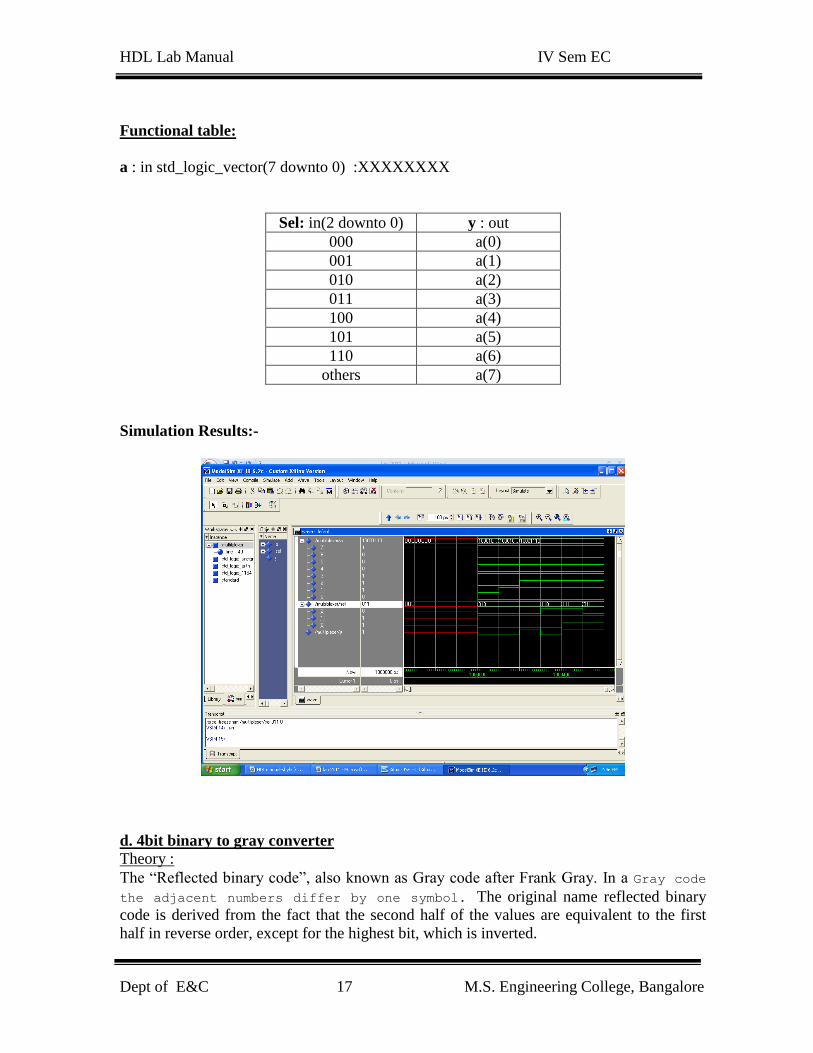
Functional table:
a : in std_logic_vector(7 downto 0) :XXXXXXXX
Sel: in(2 downto 0) y : out
000 a(0)
001 a(1)
010 a(2)
011 a(3)
100 a(4)
101 a(5)
110 a(6)
others a(7)
Simulation Results:-
d. 4bit binary to gray converter
Theory :
The “Reflected binary code”, also known as Gray code after Frank Gray. In a Gray code
the adjacent numbers differ by one symbol. The original name reflected binary
code is derived from the fact that the second half of the values are equivalent to the first
half in reverse order, except for the highest bit, which is inverted.

HDL Lab Manual IV Sem EC
Dept of E&C 18 M.S. Engineering College, Bangalore
Applications: Some sensors send information in Gray code. These must be
converted to binary in order to do arithmetic operations. Gray codes are
widely used to facilitate error correction in digital communications.
VHDL program :
entity bintogray is
port(b : in std_logic_vector(3 downto 0);
g : out std_logic_vector(3 downto 0)
);
end bintogray ;
architecture behavioral of bintogray is
begin
g(3)<=b(3);
g(2)<=b(3) xor b(2);
g(1)<=b(2) xor b(1);
g(0)<=b(1) xor b(0);
end behavioral;
Verilog Code
module bintogray(a, b);
input [3:0] a;
output [3:0] g;
assign g(3)=b(3);
assign g(2)=b(3) ^ b(2);
assign g(1)=b(2) ^ b(1);
assign g(0)=b(1) ^ b(0);
endmodule
Functional table:
Decimal Binary Gray
0 0000 0000
1 0001 0001
2 0010 0011
3 0011 0010
4 0100 0110
5 0101 0111
6 0110 0101
7 0111 0100
8 1000 1100
9 1001 1101
10 1010 1111
11 1011 1110
12 1100 1010
13 1101 1011

HDL Lab Manual IV Sem EC
Dept of E&C 19 M.S. Engineering College, Bangalore
14 1110 1001
15 1111 1000
Simulation Results:-
e.1) Demux 4:1
library ieee;
use ieee.std_logic_1164.all;
use ieee.std_logic_arith.all;
use ieee.std_logic_unsigned.all;
entity demuxI4 is
port(din : in std_logic;
s: in std_logic_vector(1 downto 0);
dout: out std_logic_vector(3 downto 0));
end demuxI4;
architecture behavioral of demuxI4 is
begin
process(din, s)
begin
case s is

HDL Lab Manual IV Sem EC
Dept of E&C 20 M.S. Engineering College, Bangalore
when"00"=>dout(0)<=din;
when"01"=>dout(1)<=din;
when"10"=>dout(2)<=din;
when others=>dout(3)<=din;
end case;
end process;
end behavioral;
Verilog code
module demux(din, s, dout);
input din;
input [1:0] s;
output [3:0] dout;
reg [3:0] dout;
always @ (din or s)
case(s)
2‟b00: dout(0)=din;
2‟b01: dout(1)=din;
2‟b10: dout(2)=din;
2‟b11: dout(3)=din;
endcase
endmodule
Functional Table:
din: 0/1
s : (in) dout (output)
00 dout(0)
01 dout(1)
10 dout(2)
11 dout(3)
Simulation results:

HDL Lab Manual IV Sem EC
Dept of E&C 21 M.S. Engineering College, Bangalore
e.2) Comparator
entity compar is
port(a, b: in std_logic_vector(3 downto 0);
aeqb, agtb, altb : out std_logic
);
end compar;
architecture behavioral of compar is
begin
aeqb<='1' when a=b else '0';
agtb<='1' when a>b else '0';
altb<='1' when a<b else '0';
end behavioral;
Functional Table:
a:input
(3downto0)
b:input
(3downto0)
aeqb agtb altb
1111 1100 0 1 0
1111 1111 1 0 0
0000 1111 0 0 1
HDL Lab Manual IV Sem EC
Dept of E&C 22 M.S. Engineering College, Bangalore
Simulation Results:-
Experiment No 3:
Write and simulate a HDL model for Full adder using three different modeling
styles.
Objective: - To write and simulate the HDL model for Full adder using three different modeling
styles
Theory: -
full adder is the basic combinational arithmetic block used in digital design the
purpose of this model is to take three inputs (input A, input B and carry in) and
provide the two outputs (sum and carryout).sum will be the arithmetic addition of
all the three inputs and the carryout will be the overflow of value in the sum.
Program in VHDL:-
entity fulladd17 is
Port ( a : in STD_LOGIC;
b : in STD_LOGIC;
c : in STD_LOGIC;
sum : out STD_LOGIC;
carry : out STD_LOGIC);

HDL Lab Manual IV Sem EC
Dept of E&C 23 M.S. Engineering College, Bangalore
end fulladd17;
architecture Behavioral of fulladd17 is
begin
process (a,b,c)
variable var:std_logic_vector(2 downto 0);
begin
var :=a&b&c;
case (var) is
when "000"=>
sum<='0';
carry<='0';
when "001"|"010"|"100"=>
sum<='1';
carry<='0';
when "011"|"101"|"110"=>
sum<='0';
carry<='1';
when "111"=>
sum<='1';
carry<='1';
when others =>null;
end case;
end process;
end Behavioral;
b. Structural Modeling.
Half adder dataflow modeling
library ieee;
use ieee.std_logic_1164.all;
use ieee.std_logic_arith.all;
use ieee.std_logic_unsigned.all;
entity ha is
port(a,b : in std_logic;
s, co: out std_logic
);
end ha;
architecture behavioral of ha is
begin
s=a xor b;
co<=a and b;
HDL Lab Manual IV Sem EC
Dept of E&C 24 M.S. Engineering College, Bangalore
end behavioral;
Full adder using two half adders (Structural Modeling)
library ieee;
use ieee.std_logic_1164.ALL;
use ieee.std_logic_arith.all;
use ieee.std_logic_unsigned.all;
entity fa is
port(x, y, cin :in std_logic;
sum, cout :out std_logic);
end fa;
architecture behavioral of fa is
component ha
port(x, y:in std_logic;
s, co : out std_Logic
);
end component;
signal tl,t2,t3:std_logic;
begin
fal: ha port map(x, y, tl, t2);
fa2: ha port map(tl, cin, s, t3);
co<=t2 or t3;
end behavioral;
Verilog code
module fa(x, y, cin, sum, cout);
input x, y, cin;
output sum, carry;
wire t1, t2, t3;
xor (t1, x, y);
and (t3, x, y);
xor (sum, t1, cin);
and (t2, t1, cin);
or (carry, t2, t3);
endmodule
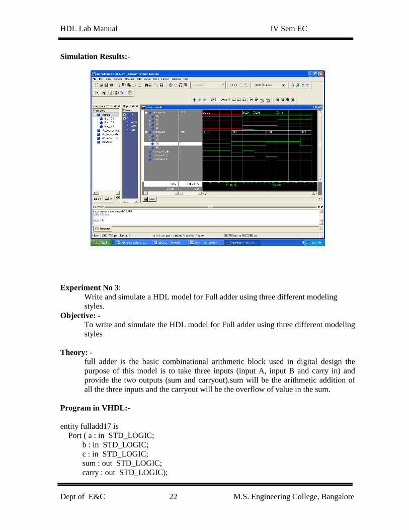
Simulation Results:-

HDL Lab Manual IV Sem EC
Dept of E&C 25 M.S. Engineering College, Bangalore
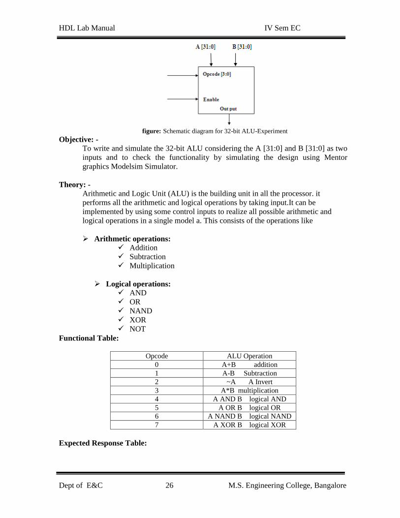
Experiment No 4:
Write and simulate a model for 32-bit ALU using the schematic diagram shown
below with input A [31:0] and B [31:0].
HDL Lab Manual IV Sem EC
Dept of E&C 26 M.S. Engineering College, Bangalore
figure: Schematic diagram for 32-bit ALU-Experiment
Objective: - To write and simulate the 32-bit ALU considering the A [31:0] and B [31:0] as two
inputs and to check the functionality by simulating the design using Mentor
graphics Modelsim Simulator.
Theory: -
Arithmetic and Logic Unit (ALU) is the building unit in all the processor. it
performs all the arithmetic and logical operations by taking input.It can be
implemented by using some control inputs to realize all possible arithmetic and
logical operations in a single model a. This consists of the operations like
Arithmetic operations:
Addition
Subtraction
Multiplication
Logical operations:
AND
OR
NAND
XOR
NOT
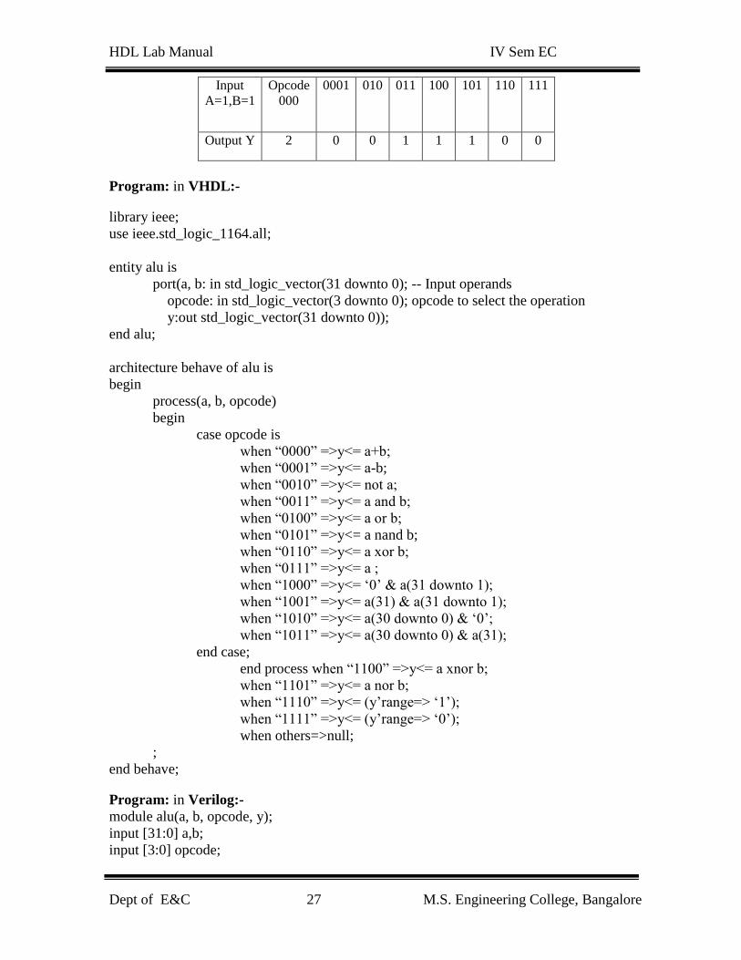
Functional Table:
Opcode ALU Operation
0 A+B addition
1 A-B Subtraction
2 ~A A Invert
3 A*B multiplication
4 A AND B logical AND
5 A OR B logical OR
6 A NAND B logical NAND
7 A XOR B logical XOR
Expected Response Table:
HDL Lab Manual IV Sem EC
Dept of E&C 27 M.S. Engineering College, Bangalore
Input
A=1,B=1
Opcode
000
0001 010 011 100 101 110 111
Output Y 2 0 0 1 1 1 0 0
Program: in VHDL:-
library ieee;
use ieee.std_logic_1164.all;
entity alu is
port(a, b: in std_logic_vector(31 downto 0); -- Input operands
opcode: in std_logic_vector(3 downto 0); opcode to select the operation
y:out std_logic_vector(31 downto 0));
end alu;
architecture behave of alu is
begin
process(a, b, opcode)
begin
case opcode is
when “0000” =>y<= a+b;
when “0001” =>y<= a-b;
when “0010” =>y<= not a;
when “0011” =>y<= a and b;
when “0100” =>y<= a or b;
when “0101” =>y<= a nand b;
when “0110” =>y<= a xor b;
when “0111” =>y<= a ;
when “1000” =>y<= „0‟ & a(31 downto 1);
when “1001” =>y<= a(31) & a(31 downto 1);
when “1010” =>y<= a(30 downto 0) & „0‟;
when “1011” =>y<= a(30 downto 0) & a(31);
end case;
end process when “1100” =>y<= a xnor b;
when “1101” =>y<= a nor b;
when “1110” =>y<= (y‟range=> „1‟);
when “1111” =>y<= (y‟range=> „0‟);
when others=>null;
;
end behave;
Program: in Verilog:-
module alu(a, b, opcode, y);
input [31:0] a,b;
input [3:0] opcode;
HDL Lab Manual IV Sem EC
Dept of E&C 28 M.S. Engineering College, Bangalore
output [31:0] y;
reg [31:0] y;
always @ (a or b or opcode)
begin
case (opcode )
4'b0000: y=a+b;
4'b0001: y=a-b;
4'b0010: y=~a;
4'b0011: y=a &b;
4'b0100: y=a | b;
4'b0101: y=~(a & b);
4'b0110: y=~(a | b);
4'b0111: y=a ^ b;
4'b1000: y=~(a ^ b);
4'b1001: y=a;
4'b1010: y=32'b00000000000000000000000000000000;
4'b1011: y=32'b11111111111111111111111111111111;
4'b1100: y=a+1;
4'b1101: y=a-1;
4'b1110: y=b+1;
4'b1111: y=b-1;
default: y=32'bX;
endcase
end
endmodule
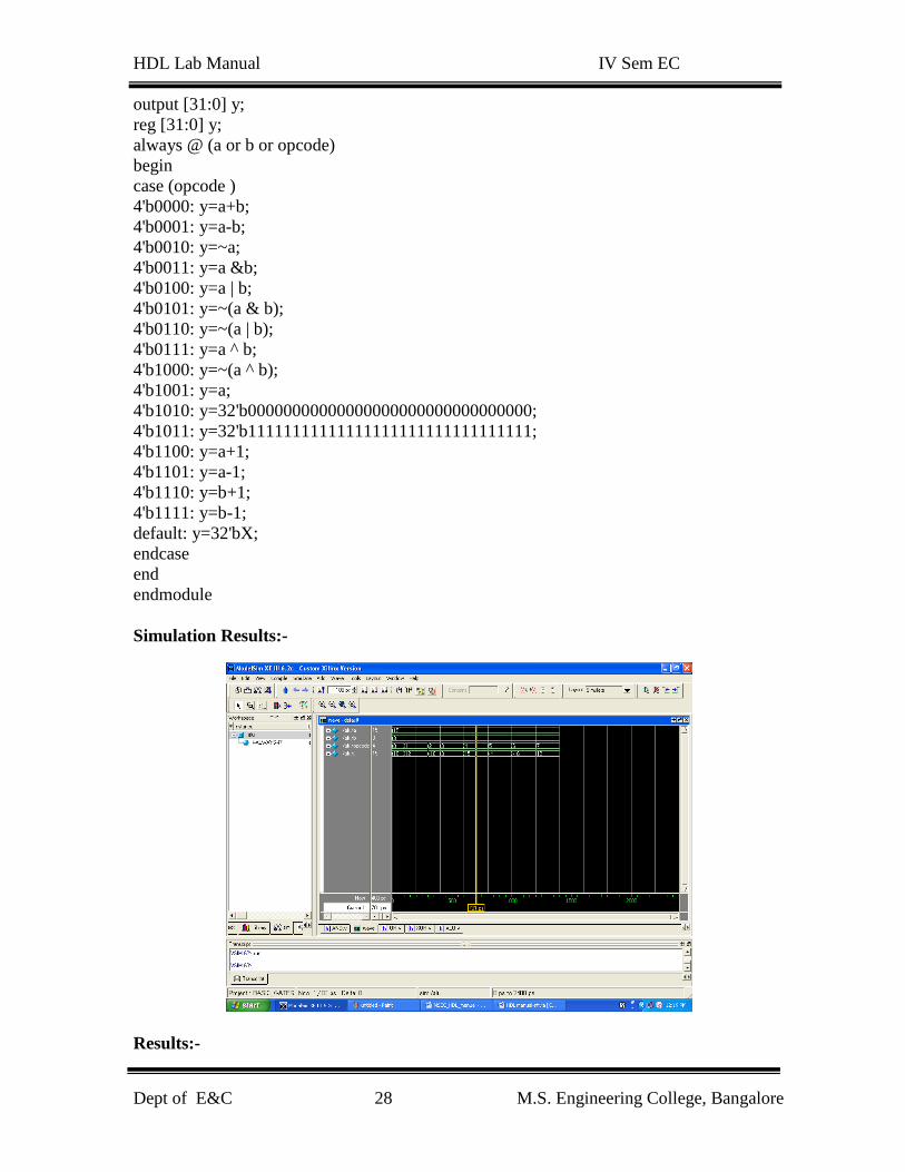
Simulation Results:-
Results:-
HDL Lab Manual IV Sem EC
Dept of E&C 29 M.S. Engineering College, Bangalore
Written and simulated the HDL model for the 32-bit ALU and verified the
simulation results for functional correctness by comparing the .
Experiment No 5:
Objective: - Develop and simulate the HDL code for the following flip-flops
SR
JK
D
T
Theory: - SR flip-flop: A SR flip-flop is the simplest possible memory element. The SR flip flop has two inputs Set and
Reset. The SR flip-flop is a basic building block for other flip-flops.
D flip-flop: This is a flip-flop with a delay (D) equal to exactly equal to one cycle of the clock. The defect
with SR FF is the indeterminate output when the data inputs at S and R are 1. In order to avoid this the input
to R is through an inverter from S so that the input to R is always the complement of S and never same. The S
input is redesignated as D.
JK flip-flop: The JK flip-flop is called a “universal flip flop” because the other flip flops like D, SR, T can be
derived from it. The “racing or race around condition” takes place in a JK FF when J=1 and K=1 and
clock=1.
T flip-flop: T stands for toggling. It is obtained from JK FF by tying both the inputs J and K.
S-R flip-flop Truth table:
Input
S
Input
R
Output
Q
0 0 0
0 1 0
1 0 1
1 1 z
Program in VHDL:- library ieee;
use ieee.std_logic_1164.all;
use ieee.std_logic_arith.all;
use ieee.std_logic_unsigned.all;
entity srff is
port(rst, s, r, pr : in std_logic;
clk : in std_logic;
q : inout std_logic;
qn: inout std_logic
HDL Lab Manual IV Sem EC
Dept of E&C 30 M.S. Engineering College, Bangalore
);
end srff;
architecture behavioral of srff is
begin
process(rst, pr, clk)
begin
if rst='1' then
q<='0';
qn<='1';
elsif pr= „1‟ then
q<= „1‟;
qn<= „0‟;
elsif clk='1' and clk'event then
if(s='0' and r='0')then
q<=q;
elsif(s='0' and r='1')then
q<='0';
qn<='1';
elsif(s='1' and r='0')then
q<='1';
qn<= „0‟;
elsif(s='1' and r='1')then
q<='Z';
end if;
end if;
end process;
qn <= not q;
end behavioral;
Program in Verilog:-
module srff(rst, s, r, clk, qn, q);
input s, r, rst, clk;
output q, qn;
reg ff;
assign q=ff;
assign qn=~ff;
always @ (posedge clk or posedge rst)
begin
if (rst)
ff<=1'b0;
else
case({s,r})
2'b01:ff<=1'b0;
2'b10:ff<=1'b1;
2'b11:ff<=1'bZ;
default:ff<=ff;
endcase
end
endmodule
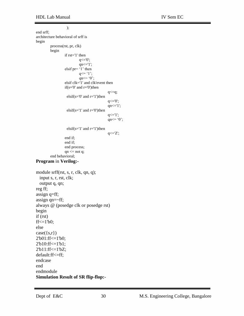
Simulation Result of SR flip-flop:-
HDL Lab Manual IV Sem EC
Dept of E&C 31 M.S. Engineering College, Bangalore
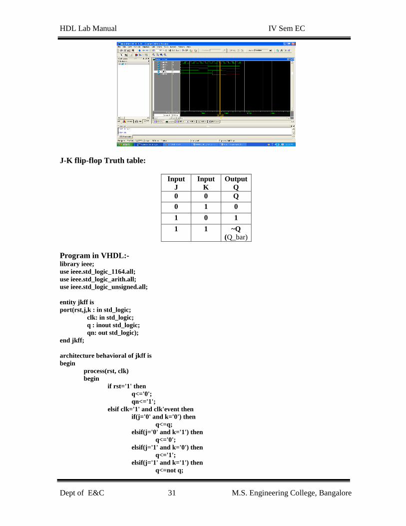
J-K flip-flop Truth table:
Input
J
Input
K
Output
Q
0 0 Q
0 1 0
1 0 1
1 1 ~Q
(Q_bar)
Program in VHDL:- library ieee;
use ieee.std_logic_1164.all;
use ieee.std_logic_arith.all;
use ieee.std_logic_unsigned.all;
entity jkff is
port(rst,j,k : in std_logic;
clk: in std_logic;
q : inout std_logic;
qn: out std_logic);
end jkff;
architecture behavioral of jkff is
begin
process(rst, clk)
begin
if rst='1' then
q<='0';
qn<='1';
elsif clk='1' and clk'event then
if(j='0' and k='0') then
q<=q;
elsif(j='0' and k='1') then
q<='0';
elsif(j='1' and k='0') then
q<='1';
elsif(j='1' and k='1') then
q<=not q;

HDL Lab Manual IV Sem EC
Dept of E&C 32 M.S. Engineering College, Bangalore
end if;
end if;
end process;
qn<=not q;
end behavioral;
Program in Verilog:-
module jkff(clk, rst, j, k, q, qn);
input clk, rst, j, k;
output q, qn;
reg ff;
assign q=ff;
assign qn=~ff;
always @ (posedge clk or posedge rst)
begin
if (rst)
ff<=1'b0;
else
case({j, k})
2'b01: ff<=1'b0;
2'b10: ff<=1'b1;
2'b11: ff<=~ff;
default: ff<=ff;
endcase
end
endmodule
Simulation Result of JK flip-flop:-
HDL Lab Manual IV Sem EC
Dept of E&C 33 M.S. Engineering College, Bangalore
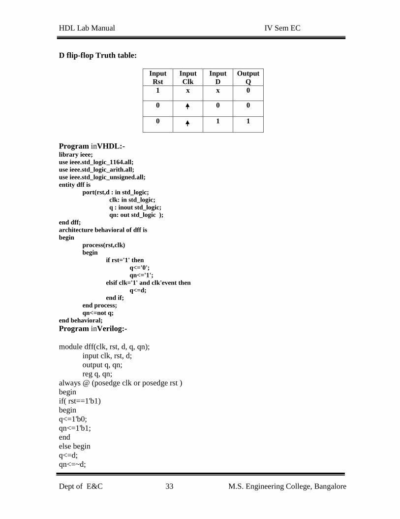
D flip-flop Truth table:
Input
Rst
Input
Clk
Input
D
Output
Q
1 x x 0
0 0 0
0 1 1
Program inVHDL:- library ieee;
use ieee.std_logic_1164.all;
use ieee.std_logic_arith.all;
use ieee.std_logic_unsigned.all;
entity dff is
port(rst,d : in std_logic;
clk: in std_logic;
q : inout std_logic;
qn: out std_logic );
end dff;
architecture behavioral of dff is
begin
process(rst,clk)
begin
if rst='1' then
q<='0';
qn<='1';
elsif clk='1' and clk'event then
q<=d;
end if;
end process;
qn<=not q;
end behavioral;
Program inVerilog:-
module dff(clk, rst, d, q, qn);
input clk, rst, d;
output q, qn;
reg q, qn;
always @ (posedge clk or posedge rst )
begin
if( rst==1'b1)
begin
q<=1'b0;
qn<=1'b1;
end
else begin
q<=d;
qn<=~d;

HDL Lab Manual IV Sem EC
Dept of E&C 34 M.S. Engineering College, Bangalore
end
end
endmodule
Simulation Result:-
T flip-flop Truth table:
Input
Rst
Input
Clk
Input
T
Output
Q
1 x x 0
0 0 1
0 1 0
Program inVHDL:- library ieee;
use ieee.std_logic_1164.all; use ieee.std_logic_arith.all;
use ieee.std_logic_unsigned.all;
entity tff is
port ( t: in std_logic; -- input t clk: in std_logic; -- global clock signal
q: out std_logic ); -- q output
end tff;
architecture t_ff_arch of tff is
begin process(clk)
begin
if(clk'event and clk='1')then
HDL Lab Manual IV Sem EC
Dept of E&C 35 M.S. Engineering College, Bangalore
q<=not t;
end if;
end process; end t_ff_arch;
Program inVerilog:-
module tff(clk, t, rst, q, qn);
input clk, rst, t;
output q, qn;
reg q, qn;
always @ (posedge clk or posedge rst)
begin
if(rst==1'b1)
begin
q<=1'b1;
qn<=1'b0;
end
else
begin
qn<=t;
q<=~t;
end
end
endmodule
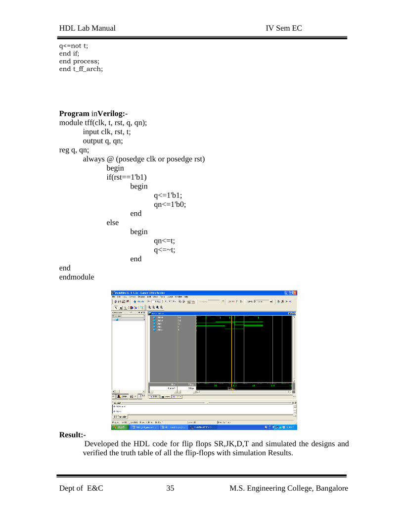
Result:-
Developed the HDL code for flip flops SR,JK,D,T and simulated the designs and
verified the truth table of all the flip-flops with simulation Results.

HDL Lab Manual IV Sem EC
Dept of E&C 36 M.S. Engineering College, Bangalore
Experiment No 6:
Objective: - Design and simulate the HDL code for a 4-bit binary, BCD counters with
Synchronous Reset
Asynchronous Reset
Any sequence
Theory: - Basically the counters are the sequential blocks where in we use to generate a sequence of numbers
with respect to the clock counts which is a control signal provided for the design. Counters can be modeled of
synchronous or Asynchronous types based on the clock applied for the design to execute the logic, Counters
can start counting not only from the zero, In fact it can be initiated to any random value to make a count from
some non-zero number and it is also possible to increment the counter with more than one in one clock
period.
4-bit Binary counter with Synchronous Reset
Program in VHDL:-
library ieee;
use ieee.std_logic_1164.all;
use ieee.std_logic_arith.all;
HDL Lab Manual IV Sem EC
Dept of E&C 37 M.S. Engineering College, Bangalore
use ieee.std_logic_unsigned.all;
entity syncnt is
generic( n:integer:=3);
port(rst : in std_logic;
clk : in std_logic;
count: out std_logic_vector(n downto 0)
);
end syncnt;
architecture behavioral of syncnt is
signal temp:std_logic_vector(n downto 0);
begin
process(clk)
begin
if clk='1' and clk'event then
if rst='1' then
temp<=(others=>'0');
else
temp<=temp+ 1 ;
end if;
count<=temp;
end if;
end process;
end behavioral;
Program in Verilog:-
module syncnt(clk, reset, qout)
input clk, reset;
output [3:0] qout;
reg [3:0] qout;
always @ (posedge clk)
begin
if(reset) begin
qout<=4„b0;
end
else
qout<=qout+1;
end
endmodule
simulation Result:-

HDL Lab Manual IV Sem EC
Dept of E&C 38 M.S. Engineering College, Bangalore
4 - bit binary counter with Asynchronous reset.
Program in VHDL:-
library ieee;
use ieee.std_logic_1164.all;
use ieee.std_logic_arith.all;
use ieee.std_logic_unsigned.all;
entity asycnt is
generic(n:integer:=3 );
port(rst : in std_logic;
clk : in std_logic;
count: out std_logic_vector(n downto 0)
);
end asycnt;
architecture behavioral of asycnt is
signal temp:std_logic_vector(n downto 0);
begin
process(rst, clk)
begin
if rst='1' then
temp<=(temp'range=>'0');
elsif clk='1' and clk'event then
temp<=temp+ 1 ;
count<=temp;
end if;
end process;
end behavioral;
Program in Verilog:-

HDL Lab Manual IV Sem EC
Dept of E&C 39 M.S. Engineering College, Bangalore
module asyncnt(clk, reset, qout);
input clk, reset;
output [3:0] qout;
reg [3:0] qout;
always @ (posedge clk or posedge reset)
begin
if(reset) begin
qout<=4'b0;
end
else
qout<=qout+1;
end
endmodule
Simulation Result:-
4-bit BCD counter with Synchronous reset.
Program in VHDL:-
library ieee;
use ieee.std_logic_1164.all;
use ieee.std_logic_arith.all;
use ieee.std_logic_unsigned.all;
entity bcdsyncnt is
generic(n:integer:=3 );
port(rst : in std_logic;
clk : in std_logic;
count: out std_logic_vector(n downto 0)
);
end bcdsyncnt;
architecture behavioral of bcdsyncnt is
HDL Lab Manual IV Sem EC
Dept of E&C 40 M.S. Engineering College, Bangalore
signal temp:std_logic_vector(n downto 0);
begin
process(clk)
begin
if clk='1' and clk'event then
if rst='1' then
temp<=( others=>'0');
else
temp<=temp+ 1 ;
if temp="1001" then
temp<=( others=>'0');
end if;
end if;
count<=temp;
end if;
end process;
end behavioral;
Program in Verilog:-
module syncnt_bcd(clk, reset, qout);
input clk, reset;
output [3:0] qout;
reg [3:0] temp;
assign qout=temp;
always @ (posedge clk)
begin
if(reset)
begin
temp<=4'b0000;
end
else
begin
temp<=temp+1'b1;
if(temp==4'b1001)
temp<=4'b0000;
end
end
endmodule

HDL Lab Manual IV Sem EC
Dept of E&C 41 M.S. Engineering College, Bangalore
4-bit BCD counter with Asynchronous reset.
Program in VHDL:-
library ieee;
use ieee.std_logic_1164.all;
use ieee.std_logic_arith.all;
use ieee.std_logic_unsigned.all;
entity bcdasycnt is
generic( n: integer:=3);
port(rst : in std_logic;
clk : in std_logic;
count: out std_logic_vector(n downto 0)
);
end bcdasycnt;
architecture behavioral of bcdasycnt is
signal temp:std_logic_vector(n downto 0);
begin
process(rst,clk)
begin
if rst='1' then
temp<=(temp'range=>'0');
elsif clk='1' and clk'event then
temp<=temp+ 1 ;
if temp="1001" then
temp<=(temp'range=>'0');
end if;
count<=temp;
end if;
end process;
end behavioral;
Program in Verilog:-

HDL Lab Manual IV Sem EC
Dept of E&C 42 M.S. Engineering College, Bangalore
module Asyncnt_bcd(clk, reset, qout);
input clk, reset;
output [3:0] qout;
reg [3:0] temp;
assign qout=temp;
always @ (posedge clk or posedge reset)
begin
if(reset)
begin
temp<=4'b0000;
end
else
begin
temp<=temp+1'b1;
if(temp==4'b1001)
temp<=4'b0000;
end
end
endmodule
Simulation Result:-
Result: - Designed and simulated the HDL code for a 4-bit binary, BCD counters with
Synchronous Reset
Asynchronous Reset
And verified the simulation Results for the counting sequence and the
Synchronous and Asynchronous counting.

HDL Lab Manual IV Sem EC
Dept of E&C 43 M.S. Engineering College, Bangalore
Interfacing Experiments:
Experiment No 1:-
Write, Implement and Interface the HDL Design to display a message on seven
segment Display and LCD display by accepting input from Hex key pad.
Objective: - To Write, Implement and Interface the HDL Design on FPGA to display a message
on seven segment Display and LCD display by accepting input from Hex key pad.
Theory: -
FPGA (Field Programmable Gate Array) is the prototyping device used very rapidly
in the Industry to check the most of the applications now a day. It is made up of Basic
block called Basic Logic Element (BLE). Which consists of LUT (Look Up Table), Mux
(Multiplexer), and then a Register element (Flip-flop).Because of its fast computing
capability most of the advanced applications will be implemented on FPGA. Once the
Design is programmed in a Bit format onto FPGA using implementing software (Xilinx),
now FPGA will act as a prototype of the design. Since it holds some functionality it can
drive some functionality onto external hard ware with help of set of I/O (input and output)
pins and some control pins available on FPGA, We call this as interfacing of FPGA with
external hard ware like LCD (Liquid Crystal Display) and Seven Segment Display, DC
Motor, Stepper Motor, DAC (Digital to analog converter), Elevator demo board.
Program in VHDL:-
entity lcda is
Port ( plcddat : out STD_LOGIC_VECTOR (7 downto 0);
plcdrs,plcdrw,plcden : out STD_LOGIC;
pclk100k : in STD_LOGIC);
end lcda;
architecture Behavioral of lcda is
signal sclkdiv: STD_LOGIC_VECTOR (15 downto 0);
signal sdspclk: STD_LOGIC;
signal tchrl: character;
constant mystr:string:="MSEC";
begin
HDL Lab Manual IV Sem EC
Dept of E&C 44 M.S. Engineering College, Bangalore
process(pclk100k)
begin
if(rising_edge(pclk100k))then
sclkdiv<=sclkdiv+1;
end if;
sdspclk<=sclkdiv(15);
plcden<=sclkdiv(15);
end process;
process(sdspclk)
variable vdspseq : integer range 0 to 15;
variable vdspnum : integer range 0 to 15;
variable i1 : integer;
type tlcdtyp is array(0 to 15) of std_logic_vector(7 downto 0);
constant tlcddat :tlcdtyp :=("00111000","00001110","00000010","00000001",
"01000001","01000100","01001101","00100000",
"01000001","01000100","01001101","00100000",
"01000001","01000100","01001101","00100000");
begin
if(falling_edge(sdspclk)) then
vdspseq := vdspseq+1;
end if;
if(falling_edge(sdspclk)) then
if(vdspseq>3) then
vdspnum := vdspnum+1;
end if;
end if;
if (vdspseq<4) then
plcddat<=tlcddat(vdspseq);
vdspnum := 1;
else
plcddat<=tlcddat(vdspseq);
tchrl<=mystr(vdspnum);
plcddat<=std_logic_vector(to_unsigned(character'pos(tchrl),8));
end if;
plcdrw<='0';
if (vdspseq<=4) then
plcdrs<='0';
else
HDL Lab Manual IV Sem EC
Dept of E&C 45 M.S. Engineering College, Bangalore
plcdrs<='1';
end if;
end process;
end Behavioral;
Result:-
Written, Implemented the HDL Design on FPGA and Interfaced with seven
segment Display and LCD display and displayed the message by accepting input
from Hex key pad. Found the hard ware working and compared the output.
Experiment No 2:-
Write, Implement and Interface the HDL Design to control the speed and direction
of DC and Stepper motor.
Objective: - To Write, Implement and Interface the HDL Design to control the speed and
direction of DC and Stepper motor.
Program in VHDL for DC Motor:-
library IEEE;
use IEEE.STD_LOGIC_1164.ALL;
use IEEE.STD_LOGIC_ARITH.ALL;
use IEEE.STD_LOGIC_UNSIGNED.ALL;
---- Uncomment the following library declaration if instantiating
---- any Xilinx primitives in this code.
--library UNISIM;
--use UNISIM.VComponents.all;
entity dc5 is
port(psw:in std_logic_vector(2 downto 0);
dcm:out std_logic;
clk:in std_logic);
end dc5;
architecture Behavioral of dc5 is
signal sclkdiv:std_logic_vector(11 downto 0);
begin
process (clk)
begin
if(rising_edge(clk))
HDL Lab Manual IV Sem EC
Dept of E&C 46 M.S. Engineering College, Bangalore
then
sclkdiv<=sclkdiv+1;
end if;
if(sclkdiv="101110111000")
then
sclkdiv<="000000000000";
end if;
end process;
process(psw,sclkdiv)
variable vdcm:bit;
begin
if(sclkdiv="000000000000")then
vdcm:='1';
end if;
if(psw="000" and sclkdiv="000111110100")then vdcm:='0';
elsif(psw="001" and sclkdiv="001100100000")then vdcm:='0';
elsif(psw="010" and sclkdiv="010001001100")then vdcm:='0';
elsif(psw="011" and sclkdiv="010101111000")then vdcm:='0';
elsif(psw="100" and sclkdiv="011010100100")then vdcm:='0';
elsif(psw="101" and sclkdiv="011111010000")then vdcm:='0';
elsif(psw="110" and sclkdiv="100011111100")then vdcm:='0';
elsif(psw="111" and sclkdiv="100111000100")then vdcm:='0';
end if;
if(vdcm='1') then dcm<='1';
else dcm<='0';
end if;
end process;
end Behavioral;
Program in VHDL for Stepper Motor:-
--------------------------------------------------------------------------------
library IEEE;
use IEEE.STD_LOGIC_1164.ALL;
use IEEE.STD_LOGIC_ARITH.ALL;
use IEEE.STD_LOGIC_UNSIGNED.ALL;
---- Uncomment the following library declaration if instantiating
---- any Xilinx primitives in this code.
--library UNISIM;
--use UNISIM.VComponents.all;
entity stepnew is
Port ( clk : in STD_LOGIC;
reset : in STD_LOGIC;
dir : in STD_LOGIC;
row : in STD_LOGIC_VECTOR (1 downto 0);
dout : out STD_LOGIC_VECTOR (3 downto 0));

HDL Lab Manual IV Sem EC
Dept of E&C 47 M.S. Engineering College, Bangalore
end stepnew;
architecture Behavioral of stepnew is
------------signal declarartion statements-------
signal clk_div: std_logic_vector(25 downto 0);
signal clk_int:std_logic;
signal shift_reg:std_logic_vector(3 downto 0);
begin
process(clk)
begin
if rising_edge(clk)then
clk_div<=clk_div+'1';
end if;
end process;
clk_int<=clk_div(25) when row="00" else
clk_div(15) when row="01" else
clk_div(10) when row="10" else
clk_div(10) ;
process(reset,clk_int,dir)
begin
if reset='0'then
shift_reg<="1001";
elsif rising_edge(clk_int) then
if dir='0' then
shift_reg<=shift_reg (0) & shift_reg (3 downto 1);
else
shift_reg<=shift_reg (2 downto 0) & shift_reg (3);
end if;
end if;
end process;
dout<=shift_reg;
end Behavioral;
User constraints file:-
#pin2ucf –
NET "clk" LOC = P77;
NET "dir" LOC = P3;
NET "dout<0>" LOC = P4;
NET "dout<1>" LOC = P5;
NET "dout<2>" LOC = P7;
NET "dout<3>" LOC = P8;
NET "reset" LOC = P9;
NET "row<0>" LOC = P14;
NET "row<1>" LOC = P15;

HDL Lab Manual IV Sem EC
Dept of E&C 48 M.S. Engineering College, Bangalore
Result:-
Written, Implemented the HDL Design on FPGA and Interfaced with DC motor and
Stepper motor through Demo boards. Found the hard ware working and compared
the output.
Experiment No 3:-
Write, Implement and Interface the HDL Design to Generate different wave forms
(sine, square, triangle, ramp etc.,) using DAC change frequency and amplitude.
Objective: - To Write, Implement and Interface the HDL Design to generate different wave
forms (sine, square, triangle, ramp etc.,) using DAC change frequency and
amplitude.
Program in VHDL for sine wave:-
library IEEE;
use IEEE.STD_LOGIC_1164.ALL;
use IEEE.STD_LOGIC_ARITH.ALL;
use IEEE.STD_LOGIC_UNSIGNED.ALL;
---- Uncomment the following library declaration if instantiating
---- any Xilinx primitives in this code.
--library UNISIM;
--use UNISIM.VComponents.all;
entity ssine1 is
Port ( clk : in std_logic;
rst : in std_logic;
HDL Lab Manual IV Sem EC
Dept of E&C 49 M.S. Engineering College, Bangalore
dac_out : out std_logic_vector(0 to 7));
end ssine1;
architecture Behavioral of ssine1 is
signal c1:std_logic_vector(7 downto 0);
signal I : integer range 0 to 179;
type sine is array(0 to 179)of integer range 0 to 255;
constant value: sine
:=(128,132,136,141,154,150,154,158,163,167,171,175,180,184,188,192,195,199,203,206,2
10,213,216,220,223,226,228,231,234,236,238,241,243,244,246,247,248,249,250,251,252,2
53,254,255,255,255,255,255,254,254,253,252,251,249,246,244,243,241,238,236,234,231,2
28,226,223,220,216,213,210,206,203,199,195,192,188,184,180,175,171,167,163,158,154,1
50,145,141,136,132,128,123,119,114,110,105,101,97,92,88,84,80,75,71,67,64,60,56,52,49,
45,42,39,35,32,29,27,24,21,19,17,14,12,11,09,07,06,04,03,02,01,01,0,0,0,0,0,0,0,0,1,1,2,3,
4,6,7,9,11,12,14,17,19,21,24,27,29,32,35,39,42,45,49,52,56,60,64,67,71,75,80,84,88,92,97,
101,105,110,114,119,123,128);
begin
process(clk,rst)
begin
if(rst='1') then
c1<=(others =>'0');
elsif (clk'event and clk ='1')then
c1<=c1+1;
end if;
end process;
process(c1(3))
begin
if(c1(3)'event and c1(3)='1')then
dac_out<= conv_std_logic_vector(value(I),8);
I<=I+1;
if(I=179) then
I<=0;
end if;
end if;
end process;
end behavioral;
user cionstraints file:-
pin2ucf –
NET "clk" LOC = P77;
NET "rst" LOC = P15;
NET "dac_out<0>" LOC = P3;
NET "dac_out<1>" LOC = P4;
NET "dac_out<2>" LOC = P5;
NET "dac_out<3>" LOC = P7;
NET "dac_out<4>" LOC = P8;

HDL Lab Manual IV Sem EC
Dept of E&C 50 M.S. Engineering College, Bangalore
NET "dac_out<5>" LOC = P9;
NET "dac_out<6>" LOC = P10;
NET "dac_out<7>" LOC = P14;
Program in VHDL for square wave:-
entity ssq1 is
Port ( clk : in std_logic;
rst : in std_logic;
dac_out : out std_logic_vector(0 to 7));
end ssq1;
architecture Behavioral of ssq1 is
signal temp:std_logic_vector(3 downto 0);
signal counter:std_logic_vector(0 to 7);
signal en:std_logic;
begin
process (clk)
begin
if rising_edge(clk)then
temp <= temp +'1';
end if;
end process;
process(temp(3),rst)
begin
if rst='1' then
counter<="00000000";
elsif rising_edge(temp(3)) then
if counter<255 and en='0' then
counter<=counter+1;
en<='0';
dac_out<="00000000";
elsif counter=0 then
en<='0';
else
en<='1';
counter<=counter-1;
dac_out<="11111111";
end if;
end if;
end process;
end Behavioral;
User constraints file:-
#pin2ucf

HDL Lab Manual IV Sem EC
Dept of E&C 51 M.S. Engineering College, Bangalore
NET "clk" LOC = P77;
NET "rst" LOC = P15;
NET "dac_out<0>" LOC = P3;
NET "dac_out<1>" LOC = P4;
NET "dac_out<2>" LOC = P5;
NET "dac_out<3>" LOC = P7;
NET "dac_out<4>" LOC = P8;
NET "dac_out<5>" LOC = P9;
NET "dac_out<6>" LOC = P10;
NET "dac_out<7>" LOC = P14;
Program in VHDL for Triangular wave:-
library IEEE;
use IEEE.STD_LOGIC_1164.ALL;
use IEEE.STD_LOGIC_ARITH.ALL;
use IEEE.STD_LOGIC_UNSIGNED.ALL;
---- Uncomment the following library declaration if instantiating
---- any Xilinx primitives in this code.
--library UNISIM;
--use UNISIM.VComponents.all;
entity stria is
Port ( clk : in STD_LOGIC;
rst : in STD_LOGIC;
dac : out STD_LOGIC_VECTOR (0 to 7));
end stria;
architecture Behavioral of stria is
signal temp:std_logic_vector(3 downto 0):="0000";
signal counter:std_logic_vector(0 to 8):="000000000";
signal en:std_logic;
begin
process(clk)
begin
if rising_edge(clk)then
temp<=temp+'1';
end if;
end process;
process(temp(3))
begin
if rst='1' then counter<="000000000";

HDL Lab Manual IV Sem EC
Dept of E&C 52 M.S. Engineering College, Bangalore
elsif rising_edge(temp(3)) then
counter<=counter+1;
if counter(0)='1' then
dac<=counter( 1 to 8);
else
dac<=not(counter(1 to 8));
end if;
end if;
end process;
end Behavioral;
User constraints file:-
#pin2ucf
NET "clk" LOC = P77;
NET "rst" LOC = P15;
NET "dac<0>" LOC = P3;
NET "dac<1>" LOC = P4;
NET "dac<2>" LOC = P5;
NET "dac<3>" LOC = P7;
NET "dac<4>" LOC = P8;
NET "dac<5>" LOC = P9;
NET "dac<6>" LOC = P10;
NET "dac<7>" LOC = P14;
Program in VHDL for Ramp signal:-
library IEEE;
use IEEE.STD_LOGIC_1164.ALL;
use IEEE.STD_LOGIC_ARITH.ALL;
use IEEE.STD_LOGIC_UNSIGNED.ALL;
---- Uncomment the following library declaration if instantiating
---- any Xilinx primitives in this code.
--library UNISIM;
--use UNISIM.VComponents.all;
entity ramps1 is
Port ( clk : in STD_LOGIC;
rst : in STD_LOGIC;
dac : out STD_LOGIC_VECTOR (0 to 7));
end ramps1;
architecture Behavioral of ramps1 is
signal temp:std_logic_vector(3 downto 0):="0000";
signal cnt:std_logic_vector(0 to 7):="00000000";

HDL Lab Manual IV Sem EC
Dept of E&C 53 M.S. Engineering College, Bangalore
begin
process(clk)
begin
if rising_edge(clk)then
temp<=temp+'1';
end if;
end process;
process(temp(3),cnt)
begin
if rst='1' then cnt<="00000000";
elsif rising_edge(temp(3)) then
cnt<=cnt+15;
end if;
end process;
dac<=cnt;
end Behavioral;
User constraints file:-
#pin2ucf
NET "clk" LOC = P77;
NET "rst" LOC = P15;
NET "dac<0>" LOC = P3;
NET "dac<1>" LOC = P4;
NET "dac<2>" LOC = P5;
NET "dac<3>" LOC = P7;
NET "dac<4>" LOC = P8;
NET "dac<5>" LOC = P9;
NET "dac<6>" LOC = P10;
NET "dac<7>" LOC = P14;
Result:-
Written, Implemented the HDL Design on FPGA and Interfaced with DAC to
display the Sine, Square, Triangular, ramp and displayed the output on the
oscilloscope. Found the hard ware working and compared the output.
Experiment No 4:-
Write, Implement and Interface the HDL Design to check the elevator operations.
Objective: - To Write, Implement and Interface the HDL Design to check the elevator
operations.
HDL Lab Manual IV Sem EC
Dept of E&C 54 M.S. Engineering College, Bangalore
Program in VHDL for Elevator control:-
library IEEE;
use IEEE.STD_LOGIC_1164.ALL;
use IEEE.STD_LOGIC_ARITH.ALL;
use IEEE.STD_LOGIC_UNSIGNED.ALL;
---- Uncomment the following library declaration if instantiating
---- any Xilinx primitives in this code.
--library UNISIM;
--use UNISIM.VComponents.all;
entity TKbele is
port( pkeyret : in std_logic_vector(3 downto 0);
pkeyscn : out std_logic_vector(3 downto 0);
pdspseg : out std_logic_vector(6 downto 0);
pdspmux : out std_logic_vector(3 downto 0);
pclk100k :in std_logic
);
end TKbele;
architecture Behavioral of TKbele is
signal scurflr,skeyflr: integer range 0 to 15;
signal skeyscn :std_logic_vector(3 downto 0);
signal lkeyscn :std_logic_vector(3 downto 0);
signal lkeyret :std_logic_vector(3 downto 0);
signal sclkdiv :std_logic_vector(15 downto 0);
signal sflrclk,skeyclk,skeyhit:std_logic;
begin
--process keyprocess
process(pkeyret) --PRESS KEY RETURN
begin
case pkeyret is
when "1110"=>skeyhit <='1';
when "1101"=>skeyhit <='1';
when "1011"=>skeyhit <='1';
when "0111"=>skeyhit <='1';
when others =>skeyhit <='0';
end case;
end process;
process(skeyhit)
begin
if(rising_edge(skeyhit))then

HDL Lab Manual IV Sem EC
Dept of E&C 55 M.S. Engineering College, Bangalore
lkeyscn<=skeyscn;
lkeyret<=pkeyret;
end if;
end process;
process(skeyhit)
begin
if(rising_edge(skeyhit))then
if(lkeyscn="1110" and lkeyret ="1110" )then skeyflr <=0;
elsif(lkeyscn="1110" and lkeyret ="1101" )then skeyflr <=1;
elsif(lkeyscn="1110" and lkeyret ="1011" )then skeyflr <=2;
elsif(lkeyscn="1110" and lkeyret ="0111" )then skeyflr <=3;
elsif(lkeyscn="1101" and lkeyret ="1110" )then skeyflr <=4;
elsif(lkeyscn="1101" and lkeyret ="1101" )then skeyflr <=5;
elsif(lkeyscn="1101" and lkeyret ="1011" )then skeyflr <=6;
elsif(lkeyscn="1101" and lkeyret ="0111" )then skeyflr <=7;
elsif(lkeyscn="1011" and lkeyret ="1110" )then skeyflr <=8;
elsif(lkeyscn="1011" and lkeyret ="1101" )then skeyflr <=9;
elsif(lkeyscn="1011" and lkeyret ="1011" )then skeyflr <=10;
elsif(lkeyscn="1011" and lkeyret ="0111" )then skeyflr <=11;
elsif(lkeyscn="0111" and lkeyret ="1110" )then skeyflr <=12;
elsif(lkeyscn="0111" and lkeyret ="1101" )then skeyflr <=13;
elsif(lkeyscn="0111" and lkeyret ="1011" )then skeyflr <=14;
elsif(lkeyscn="0111" and lkeyret ="0111" )then skeyflr <=15;
end if;
end if;
end process;
--process clk driver
process(pclk100k)
begin
if(rising_edge(pclk100k))then
sclkdiv<=sclkdiv+1;
end if;
skeyclk<=sclkdiv(6);
sflrclk<=sclkdiv(15);
end process;
-- process for keyscan clkscan
process(skeyclk)
begin
if(rising_edge(skeyclk) )then
if(skeyscn)="1110"then skeyscn<="1101";
elsif(skeyscn)="1101"then skeyscn<="1011";
elsif(skeyscn)="1011"then skeyscn<="0111";
elsif(skeyscn)="0111"then skeyscn<="1110";
HDL Lab Manual IV Sem EC
Dept of E&C 56 M.S. Engineering College, Bangalore
else skeyscn<="1110";
end if;
pkeyscn<=skeyscn;
end if;
end process;
-- process florr motion
process(sflrclk)
begin
if(rising_edge(sflrclk))then
if(not(skeyflr=scurflr))then
if(skeyflr > scurflr)then scurflr<=scurflr+1;
else scurflr <=scurflr-1;
end if;
end if;
end if;
end process;
--process display 7seg
process(scurflr)
type tseg7 is array(0 to 15)of std_logic_vector(6 downto 0);
constant segval
:tseg7:=("0111111","0000110","1011011","1001111",--seg display "0","1","2","3"
"1100110","1101101","1111101","0000111",--seg display "4","5","6","7"
"1111111","1101111","1110111","1111100",--seg display "8","9","10=A","11=b"
"1011000","1011110","1111001","1110001"--seg display "12=c","13=d","14=e","15=f"
);
begin
pdspseg <=segval(scurflr);
pdspmux <="1110";
end process;
end Behavioral;
user constraints file:-
pin configurations of elevator
NET "pclk100k” LOC = "P77”;
NET "pdspmux<0>“LOC = "P33”;
NET "pdspmux<1>“LOC = "P34”;
NET "pdspmux<2>“LOC = "P35”;
NET "pdspmux<3>“LOC = "P36”;
NET "pdspseg<0>“LOC = "P41”;
NET "pdspseg<1>“LOC = "P42”;
HDL Lab Manual IV Sem EC
Dept of E&C 57 M.S. Engineering College, Bangalore
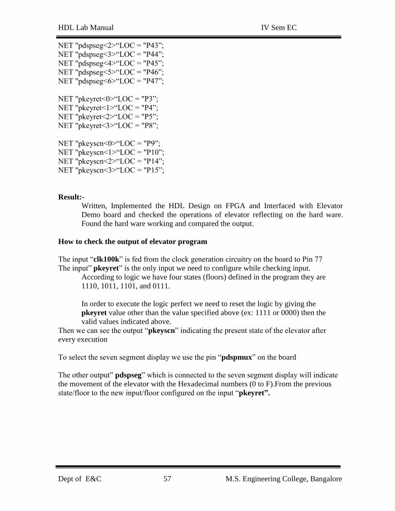
NET "pdspseg<2>“LOC = "P43”;
NET "pdspseg<3>“LOC = "P44”;
NET "pdspseg<4>“LOC = "P45”;
NET "pdspseg<5>“LOC = "P46”;
NET "pdspseg<6>“LOC = "P47”;
NET "pkeyret<0>“LOC = "P3”;
NET "pkeyret<1>“LOC = "P4”;
NET "pkeyret<2>“LOC = "P5”;
NET "pkeyret<3>“LOC = "P8”;
NET "pkeyscn<0>“LOC = "P9”;
NET "pkeyscn<1>“LOC = "P10”;
NET "pkeyscn<2>“LOC = "P14”;
NET "pkeyscn<3>“LOC = "P15”;
Result:-
Written, Implemented the HDL Design on FPGA and Interfaced with Elevator
Demo board and checked the operations of elevator reflecting on the hard ware.
Found the hard ware working and compared the output.
How to check the output of elevator program
The input “clk100k” is fed from the clock generation circuitry on the board to Pin 77
The input” pkeyret” is the only input we need to configure while checking input.
According to logic we have four states (floors) defined in the program they are
1110, 1011, 1101, and 0111.
In order to execute the logic perfect we need to reset the logic by giving the
pkeyret value other than the value specified above (ex: 1111 or 0000) then the
valid values indicated above.
Then we can see the output “pkeyscn” indicating the present state of the elevator after
every execution
To select the seven segment display we use the pin “pdspmux” on the board
The other output” pdspseg” which is connected to the seven segment display will indicate
the movement of the elevator with the Hexadecimal numbers (0 to F).From the previous
state/floor to the new input/floor configured on the input “pkeyret”.