ms diploma and semester projects offered at the ... v1.0 as of 04.05.2015 ms diploma and semester...
TRANSCRIPT

1/12
v1.0 as of 04.05.2015
MS Diploma and Semester Projects offered at the Microelectronic Systems Laboratory during the Winter 2015-2016 Students are asked to contact the project responsible to register. The majority of the projects are proposed as MS Diploma and Semester, and the amount of work will be adapted. Also, some projects can be carried out in groups of two students. Projects are proposed in six categories in the following pages.
Analog and mixed-signal circuits Digital circuits and modeling Bio-electronic interfaces and biomedical applications Fabrication technologies Industrial projects / external projects (for MSc diploma) Application development (software development)

2/12
Analog and mixed-signal circuits A1 none to report A2 - A3 - A4 - A5 -

3/12
Digital circuits and modeling D1 Digital Hardware Implementation of Optimization Algorithms
Efficient conversion of analog signals to their digital representation is important, since modern information processing is supported by digital computation. Given the recent trends, the data acquisition at high speeds has created a major bottleneck in Analog to Digital Converters (ADCs) based on the Shannon Nyquist sampling theorem. The main premise of this proposal is that the Analog to Digital conversion is no longer just a matter of hardware implementation, but it is a merging between mathematical algorithms and circuit design. With this premise in mind, we can significantly improve ADC performance by using only minor assumptions on the signal of interest. The project results have a great potential to become a milestone for future work in different domains. Project breakdown: 30% Matlab algorithm study and development 50% HDL coding 20% FPGA implementation Supervisor in charge: Cosimo Aprile Responsible teacher: Prof. Yusuf Leblebici
D2 Digital hardware study for on-chip Deep Learning Deep Learning is an emerging but practical algorithm of brain-inspired artificial neural networks, which has been introduced with the objective of developing artificial intelligence. Extensive researche has recently developed successful deep learning systems aiming at speech recognition and image classification. Future microelectronic systems could be based on an ultra-high density semiconductor logic/memory technology. To further exploit the great performances of deep learning, intelligent on-chip operations as a new type of digital hardware architecture should be established targeting an ultimately compact and resilient implementation. This project will introduce important deep learning algorithms including convolutional neural networks (CNN) and restricted Boltzmann machines (RBM), especially for hardware implementation. The student will realize the challenging implementation of the algorithm into on-chip digital hardware. One possible goal is to demonstrate big data analysis taken from a chip for the chip by the chip. A further goal is to create an autonomous system in which a semiconductor microsystem chip works to keep highly reliable intelligence. The results of this project have a great potential to prove a key technology for standalone hardware such as wearable devices, reliable IoTs (Internet-of-things) memories, biomedical applications etc.
Project cut-down: 30% Algorithm study and data analysis 50% HDL design 20% FPGA implementation

4/12
Project for 1/2 MSc diploma/semester student(s). Project responsible, Contact: Takao Marukame ([email protected]) Responsible teacher: Alexandre Schmid ([email protected])
D3 ASIC Design for Real-Time Panoramic Multi-Camera System Panoptic is a multi-camera system able to acquire and render the whole light field around the observer, using panoramic representation. The designed Panoptic prototypes are based on CMOS cell phone cameras which result in low final panorama image resolution. One of the drawbacks of Panoptic is the limited processing flexibility due to use of Virtex-5 FPGAs.
The goal of this project is to design an ASIC for the purpose of creating real-time panoramic videos. Currently working FPGA system will be provided as a reference and the ASIC will be designed to support higher resolution cameras and High Definition (Full HD) output.
The first steps of the project will include adapting the current Panoptic algorithms to the desired technology. The second step will include development of the interface IPs, such as Camera interface, HDMI display, UART, Memory controller. Finally, an open-source microcontroller openMSP430 will be included in the system.
Project cut-down: 10% Algorithm study 40% VHDL implementation, synthesis and simulation 40% Chip fabrication and measurements Project for 1 or 2 MSc diploma/semester student. Contact person: Vladan Popovic ([email protected]) Responsible professor: Yusuf Leblebici
D4 USB2/USB3 Controller for FPGA /ASIC←→ PC connection The project is realized as a part of the PANOPTIC camera project (http://lsm.epfl.ch/page-52820-en.html). The previous systems were able to interface with the PC/user via simple UART. Currently, a new, very high-resolution camera system is being designed. One of the advantages of the system will be the ability to display a Full HD 1080 resolution at 30 frames per second. This signal needs a very fast transfer to the PC in order to be processed later by the available GPU. In this project, the student will work on the state-of-the-art Virtex-7 FPGA and design a USB2/USB3 controller, which will allow fast data transfer to the PC. The student will create a new (adapt an IP core) controller and embedded it into an already existing operational system. If needed, the initialization routines for microprocessor on board will be written. The controller will be tested by sending/receiving the data stream. A small PC test application will be created for that purpose. Finally, the student will adapt the project to be portable and compatible with the ASIC design for 28nm process. Project cut-down: 30% VHDL design 50% FPGA implementation 20% C/C++ code development Project for 1 MSc diploma/semester student. Contact person: Vladan Popovic ([email protected]) Responsible professor: Yusuf Leblebici

5/12
D5 Real-time 3D cinematography on a multi-FPGA system Omnidirectional cameras developed in LSM have the capability to observe each direction with at least two cameras, with several centimeters distance from each other. This positioning allows us to mimic human eyes and observe objects with two cameras (two eyes), and create three-dimensional video reconstruction, similar to the ones seen in modern cinemas. In this project, the student will develop a new algorithm for combining camera frames, and reconstructing the 3D scene. The first steps of the project include study of the current 3D algorithms, and testing our own algorithm in Matlab / C / C++. The later steps are development and implementation of the algorithm on an already existing omnidirectional camera (C coding) Project cut-down: 40% Algorithm study 40% Matlab / C / C++ development (only one of them is necessary) 20% Real-time testing (C, basic VHDL is desired, but not obligatory) Project for 1 MSc diploma/semester student. Contact person: Vladan Popovic ([email protected]) Responsible professor: Yusuf Leblebici
D6 JPEG / PNG image compression on FPGA and SATA controller for SSD storage The project is realized as a part of the PANOPTIC camera project (http://lsm.epfl.ch/page-52820-en.html). The images acquired by the cameras are currently stored in RAW format, resulting in the large file size. Hence, an appropriate image compression should be applied to reduce the size without affecting the image quality. In this project, the student will work on the state-of-the-art Virtex-7 FPGA and design a real-time PNG (or JPEG) compression accelerator. The student will create a new core (adapt an IP core) and embedded it into an already existing operational system. Second part of the project consists of designing a small SATA controller for image storage on external SSD drive. Project cut-down: 30% Algorithm study 50% VHDL design 20% FPGA implementation Project for 1 MSc diploma/semester student. Contact person: Vladan Popovic ([email protected]) Responsible professor: Yusuf Leblebici
D7 FPGA Implementation of Real-Time Superresolution Systems The most common method is to increase the pixel density, or in other words, reducing the pixel size (spatial resolution) by fabrication techniques. It is common knowledge that the scaling effects in CMOS technology allow the semiconductor industry to make smaller devices. This rule holds for CMOS imaging applications as well, however it is known that CMOS image sensor technology is lagging behind the technology nodes in ITRS roadmap. The reason behind this lagging is very simple: current CMOS process is not imaging friendly. Reducing the pixel sizes mean less amount of light available per pixel. Furthermore, smaller size generates shot noise that reduces the image quality. There is a limit to reduce the pixel pitch without suffering the effects of shot noise. In order to satisfy the current needs of technology, Superresolution methods are introduced. In this project, student will be responsible of developing a superresolution algorithm suitable for real time implementation. The algorithm will be tested will real life sequences, with images coming from

6/12
single or multiple cameras. Furthermore, the student will design and implement the algorithm in RTL level in high-end Xilinx Virtex-7 devices, and test the system with FPGA, where the real-time feed is provided by high-end cameras.
Two examples of superresolution algorithms can be seen above. The images on the left is bicubic interpolation of the original images and the images on the right is the results of superresolution methods, obtained from real-life sequences. The student working on the project will gain knowledge about image processing, real-time hardware implementation, hardware-software codesign and high-end Virtex 7 FPGA. Project Type : Semester / Master Project
The project is organized as follows: Literature survey – 10% Matlab Implementation – 30% Digital Hardware Implementation – 60% Contact: Kerem Seyid, [email protected] Project supervisor: Prof. Yusuf Leblebici
D8 - D9 -

7/12
Bio-electronic interfaces and biomedical applications B1 Ultra low-voltage, low-power biomedical interface design based on switched-mode operational
amplifier The target of this project is to design neural recording system with supply voltage down to 0.5V and low-power consumption for next generation implant. The design strategy is to employ a novel time-domain signal processing circuit called “switched-mode operational amplifier (SMOA)” to replace the conventional OTA based design. In SMOA, voltage swing of signals is encoded into pulse width using a PWM modulator, which benefits from higher time resolution in scaled technology. Both theoretical and practical part will be explored in this project. Effort breakdown: 30% literature survey, 70% full custom circuit design Supervisor in charge: Wen-Yang Hsu Responsible teacher: Alexandre Schmid
B2 A Charge Balanced Voltage Mode Electrical Stimulator Electrical neural stimulation is the technique used to modulate neural activity by inducing an instantaneous charge imbalance. This is typically achieved by injecting a constant current and controlling the stimulation time. However, constant voltage stimulation is found to be more energy-efficient although it is challenging to control the amount of charge delivered. In order to prevent tissue damage and any long-term effects such as PH shift or electrode corrosion, the stimulation must be biphasic and charge balanced. A biphasic stimulation consists of a cathodic phase to initiate an action potential (AP) followed by an anodic phase to neutralize the injected charge in previous phase. In this project, we try to design an integrated buck and a buck-boost converter alongside a simple charge balancing method.
Project cut-down: 20% Review 30% Spice simulation 50% Layout Project for 1 MSc diploma/semester student. Contact person: Reza Ranjandish ([email protected]) Responsible supervisor: Alexandre Schmid
8/12
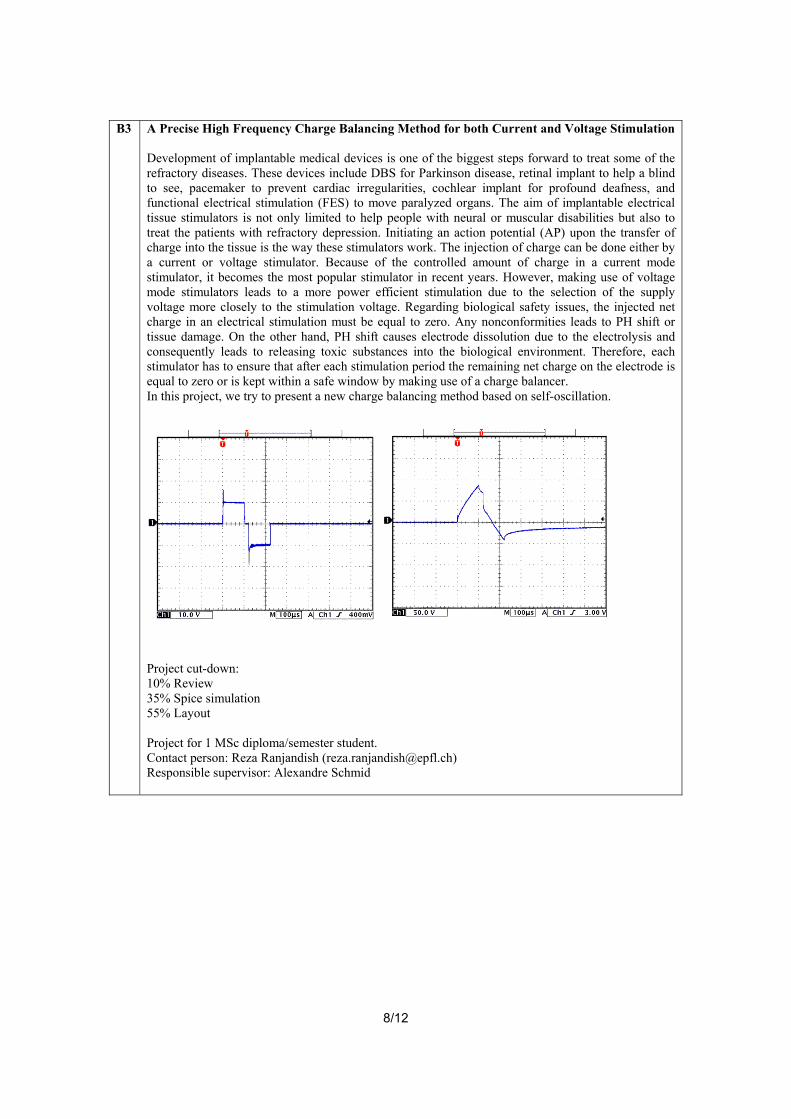
B3 A Precise High Frequency Charge Balancing Method for both Current and Voltage Stimulation Development of implantable medical devices is one of the biggest steps forward to treat some of the refractory diseases. These devices include DBS for Parkinson disease, retinal implant to help a blind to see, pacemaker to prevent cardiac irregularities, cochlear implant for profound deafness, and functional electrical stimulation (FES) to move paralyzed organs. The aim of implantable electrical tissue stimulators is not only limited to help people with neural or muscular disabilities but also to treat the patients with refractory depression. Initiating an action potential (AP) upon the transfer of charge into the tissue is the way these stimulators work. The injection of charge can be done either by a current or voltage stimulator. Because of the controlled amount of charge in a current mode stimulator, it becomes the most popular stimulator in recent years. However, making use of voltage mode stimulators leads to a more power efficient stimulation due to the selection of the supply voltage more closely to the stimulation voltage. Regarding biological safety issues, the injected net charge in an electrical stimulation must be equal to zero. Any nonconformities leads to PH shift or tissue damage. On the other hand, PH shift causes electrode dissolution due to the electrolysis and consequently leads to releasing toxic substances into the biological environment. Therefore, each stimulator has to ensure that after each stimulation period the remaining net charge on the electrode is equal to zero or is kept within a safe window by making use of a charge balancer. In this project, we try to present a new charge balancing method based on self-oscillation.
Project cut-down: 10% Review 35% Spice simulation 55% Layout Project for 1 MSc diploma/semester student. Contact person: Reza Ranjandish ([email protected]) Responsible supervisor: Alexandre Schmid

9/12
Fabrication technologies N1 Chip-level Post-CMOS Processing for 3D Integration with TSV Interconnects
Characterization and Optimization of Thermo-Compresive Parylene-C Bonding The increasing need for faster and smaller integrated circuits has resulted in continuous downscaling in transistor sizes. A new technology, namely 3D integration, has emerged since the conventional planar IC fabrication has almost reached its limits. This technology facilitates the integration of both identical (homogeneous) and heterogeneous layers. Therefore, it enables reaching higher volumetric densities and stacking different chips produced by dedicated IC technologies. Parylene-C has been used as an adhesive layer for bonding in our group in 3D integration processes. This project aims to investigate the bonding strength of parylene-C layer under different bonding conditions such as temperature and pressure. This project gives the student an opportunity of hands-on fabrication experience in the cleanroom. Experimental results may also be published in a scientific paper. Project for Semester/MSc Diploma Students Project Cutdown 60% Fabrication in the Cleanroom 40% Functionality and Characterization Testing Contact: Seniz Esra Kucuk ([email protected]) Supervisor: Y. Leblebici
N2 Chip-level Post-CMOS Processing for 3D Integration with TSV Interconnects A New Approach of TSV Fabrication for Multilayer Stacking The increasing need for faster and smaller integrated circuits has resulted in continuous downscaling in transistor sizes. A new technology, namely 3D integration, has emerged since the conventional planar IC fabrication has almost reached its limits. This technology facilitates the integration of both identical (homogeneous) and heterogeneous layers. Therefore, it enables reaching higher volumetric densities and stacking different chips produced by dedicated IC technologies. Multilayer (more than two layers) stacking has been a prodominant field in the 3D integration processes. New approaches are needed to increase multilayer stacking performance. This project aims to investigate a new approach to be applied on multilayer stacks as well as giving an opportunity to work in the cleanroom. Project for /MSc Students 20% Design 60% Fabrication in the Cleanroom 20% Functionality and Characterization Testing Contact: Seniz Esra Kucuk ([email protected]) Supervisor: Y. Leblebici
N3 3D integration of Resistive Random Access Memory (ReRAM) Recent technology is dependent on the usage of memory hierarchy. Resistive Random Access Memory (ReRAM) has gained significant attention as a leading candidate for next generation of the memory application. ReRAM allows the 3D capability, DRAM-like latency, non-volatile high storage density, compatible CMOS processing and low access power consumption. All these features of the ReRAM essentially meet the requirements for the vast applications in current technology such as classical Memory, multi-level Memory and neomorphic devices. The main operation of these devices is a resistance change induced by filament formation through metal-cations or oxygen vacancies. In this multidisciplinary project you will have the opportunity to achieve experience on state of the

10/12
art, clean room activities such as electron beam and photo lithography, dry etching techniques and electron and atomic force microscopy. In addition to the work experience in clean room, your task will be focused on CMOS post processing, 3D fabrication of ReRAM and electrical characterization of as fabricated samples.
Work description: Fabrication (50 %):
Ebeam and photo lithography
Reaction ion and wet etching
Thin film deposition Characterization (50 %):
Metrology SEM/AFM/TEM
Electrical characterization Type of project: Master project & Semester Project Section(s): Microengineering, Physics, Material science, Electrical engineering Contact: Elmira Shahrabi, ELD 333, Tel: 36936 , [email protected] Supervisor: Y. Leblebici

11/12
Industrial projects / External projects (MSc diploma) IE1 None to report

12/12
Application development (software development) SW1 Real-Time Object Tracking and Classification in omnidirectional videos using NVidia GPU
Panoptic is a multi-camera system able to acquire and render the whole light field around the observer, using panoramic representation. The designed Panoptic prototypes are based on low-cost CMOS cell phone cameras which resulted in low final panorama image resolution. One of the drawbacks of Panoptic is the limited processing flexibility due to use of Virtex-5 FPGAs. On the other hand, GPUs offer higher flexibility, faster prototyping of the envisioned algorithms, and more algorithm options. The idea of the project is to create a multi-platform processing system, with FPGA serving as a core for generating panorama. The GPU processes the panorama, detects, tracks and classifies the objects in the scene.
The project will be defined according to the student's prior knowledge of CUDA, which is not obligatory. The student will be given an already developed code for basic object tracking. The main task is adding the advanced features, such as object classification, and real-time operation. Project cut-down: 30% Algorithm study 70% CUDA programming (Prior knowledge of CUDA is not obligatory) Project for 1 MSc diploma/semester student. Contact person: Vladan Popovic ([email protected]) Responsible professor: Yusuf Leblebici
SW2 IOS Application Development for Omnidirectional Vision Reconstruction System Panoptic is a custom spherical light field camera used as a polydioptric system where imagers are distributed over a spherical geometry, each having its own vision of the surrounding and a distinct focal plane. The spherical light field camera records light information from any direction around its center. Three dimensional (3D) visualization of a full 360º scene forms the foundation for enabling the emergence of novel applications in security systems, automotive platforms and mobile robots, realistic computer games and 3D cinematography. The utilization of such systems with 360º 3D visual characteristics has recently significantly increased, with the commercialization of consumer electronics products. In this project, student will be responsible for implementing and iOS application for iPads and iPhones, for viewing the omnidirectional data in an immersive way. Currently, an Android application for the same purpose, and the Oculus Rift application is implemented for real-time omnidirectional camera as can be seen in video link. http://www.youtube.com/watch?v=yxdsymKrovA . It is expected that the student has prior knowledge for iOS app development. The student working on the project will gain knowledge about image processing, network streaming and iOS app development, as well has hardware implementation of multiple camera systems Project Type : Semester Project Software Development – 100% Contact: Kerem Seyid, [email protected] Project supervisor: Prof. Yusuf Leblebici