mp8666 6a, 21v, 600khz step-down converter · 2018-03-14 · 6a, 21v, 600khz step-down converter...
TRANSCRIPT

MP8666 6A, 21V, 600kHz Step-Down Converter with Synchronizable Gate Driver
MP8666 Rev. 1.21 www.MonolithicPower.com 1 9/21/2011 MPS Proprietary Information. Patent Protected. Unauthorized Photocopy and Duplication Prohibited. © 2011 MPS. All Rights Reserved.
The Future of Analog IC Technology
DESCRIPTION The MP8666 is a monolithic step-down switch mode converter with a built in high-side internal power MOSFET and a gate driver for a low-side external MOSFET. It achieves 6A continuous output current over a wide input supply range with excellent load and line regulation.
Current mode operation provides fast transient response and eases loop stabilization.
Fault condition protection includes cycle-by-cycle current limiting and thermal shutdown.
The MP8666 requires a minimum number of readily available standard external components and is available in an 8-pin SOIC package with exposed pad.
FEATURES • Wide 4.5V to 21V Operating Input Range • 6A Continuous Output Current • 45mΩ Internal Power MOSFET Switch • Synchronizable Gate Driver Delivers up to
95% Efficiency • Fixed 600KHz Frequency • Synchronizable up to 1.5MHz • Cycle-by-Cycle Over Current Protection with
Hiccup • Thermal Shutdown • Output Adjustable from 0.8V • Stable with Low ESR Output Ceramic
Capacitors • Available in a Thermally Enhanced 8-Pin
SOIC Package
APPLICATIONS • Point of Load Regulator in Distributed
Power System • Digital Set Top Boxes • Personal Video Recorders • Broadband Communications • Flat Panel Television and Monitors For MPS green status, please visit MPS website under Quality Assurance.“MPS” and “The Future of Analog IC Technology” are Registered Trademarks of Monolithic Power Systems, Inc.
TYPICAL APPLICATION
MP8666SW
BG
FB
BST
1
4
6
5
2
GND
IN
VCC
EN/SYNC
8
3
7
VOUT3.3V
C4100nF16V
M2
VIN
OFF ON
Efficiency vs Output Current
10095908580757065605550
EFF
ICIE
NC
Y (%
)
1 2 4 53 6OUTPUT CURRENT (A)
VIN=12V
VIN=20V
VOUT=3.3V

MP8666 – 6A, 21V, 600kHz STEP-DOWN WITH SYNCHRONIZABLE GATE DRIVER
MP8666 Rev. 1.21 www.MonolithicPower.com 2 9/21/2011 MPS Proprietary Information. Patent Protected. Unauthorized Photocopy and Duplication Prohibited. © 2011 MPS. All Rights Reserved.
ORDERING INFORMATION Part Number* Package Top Marking Free Air Temperature (TA)
MP8666DN SOIC8E MP8666DN –40°C to +85°C
* For Tape & Reel, add suffix –Z (e.g. MP8666DN–Z); For RoHS Compliant Packaging, add suffix –LF (e.g. MP8666DN–LF–Z)
PACKAGE REFERENCE
ABSOLUTE MAXIMUM RATINGS (1) Supply Voltage VIN ....................................... 23V VSW.........................-0.3V(-5V for < 10ns) to 24V VBST - VSW....................................................... 6V All Other Pins.................................–0.3V to +6V Continuous Power Dissipation (TA = +25°C)(2) SOIC8E...................................................... 2.5W Junction Temperature...............................150°C Lead Temperature ....................................260°C Storage Temperature.............. –65°C to +150°C
Recommended Operating Conditions (3) Supply Voltage VIN ...........................4.5V to 21V Operating Temperature............. –40°C to +85°C
Thermal Resistance (4) θJA θJC SOIC8E .................................. 50 ...... 10... °C/W Notes: 1) Exceeding these ratings may damage the device. 2) The maximum allowable power dissipation is a function of the
maximum junction temperature TJ(MAX), the junction-to-ambient thermal resistance θJA, and the ambient temperature TA. The maximum allowable continuous power dissipation at any ambient temperature is calculated by PD(MAX)=(TJ(MAX)-TA)/ θJA. Exceeding the maximum allowable power dissipation will cause excessive die temperature, and the regulator will go into thermal shutdown. Internal thermal shutdown circuitry protects the device from permanent damage.
3) The device is not guaranteed to function outside of its operating conditions.
4) Measured on JESD51-7, 4-layer PCB.
SW
BST
VCC
BG
IN
EN/SYNC
FB
GND
1
2
3
4
8
7
6
5
TOP VIEW
EXPOSED PADON BACKSIDE

MP8666 – 6A, 21V, 600kHz STEP-DOWN WITH SYNCHRONIZABLE GATE DRIVER
MP8666 Rev. 1.21 www.MonolithicPower.com 3 9/21/2011 MPS Proprietary Information. Patent Protected. Unauthorized Photocopy and Duplication Prohibited. © 2011 MPS. All Rights Reserved.
ELECTRICAL CHARACTERISTICS VIN = 12V, TA = +25°C, unless otherwise noted. Parameters Symbol Condition Min Typ Max UnitsFeedback Voltage VFB 4.5V ≤ VIN ≤ 21V 0.788 0.808 0.828 V Feedback Current IFB VFB = 0.8V 10 nA Switch On Resistance (5) RDS(ON) 45 mΩ Switch Leakage VEN = 0V, VSW = 0V 0 10 μA Current Limit (5) 7.5 8.0 A Oscillator Frequency fSW VFB = 0.6V 400 600 800 KHzFold-back Frequency VFB = 0V 60 150 240 KHzMaximum Duty Cycle VFB = 0.6V 85 90 % Minimum On Time (5) tON 100 ns Under Voltage Lockout Threshold Rising VCC_UVLO 3.9 4.1 4.3 V Under Voltage Lockout Threshold Hysteresis 880 mV EN Input Low Voltage 0.4 V EN Input High Voltage 1.2 V
VEN = 2V 2 EN Input Current VEN = 0V 0 μA
Sync Frequency Range (Low) FSYNCL 300 KHzSync Frequency Range (High) FSYNCH 1.5 MHzEnable Turnoff Delay TOFF 5.0 us Supply Current (Shutdown) VEN = 0V 1 10 μA Supply Current (Quiescent) VEN = 2V, VFB = 1V 0.9 1.1 mA Thermal Shutdown TJ 150 °C Thermal Shutdown Hysteresis 10 °C BG Driver Bias Supply Voltage VCC 4.5 5 V Gate Driver Sink Impedance (5) RSINK 1 Ω Gate Driver Source Impedance (5) RSOURCE 4 Ω Gate Drive Current Sense Trip Threshold VSW 20 mV
Note: 5) Guaranteed by design.
MP8666 – 6A, 21V, 600kHz STEP-DOWN WITH SYNCHRONIZABLE GATE DRIVER
MP8666 Rev. 1.21 www.MonolithicPower.com 4 9/21/2011 MPS Proprietary Information. Patent Protected. Unauthorized Photocopy and Duplication Prohibited. © 2011 MPS. All Rights Reserved.
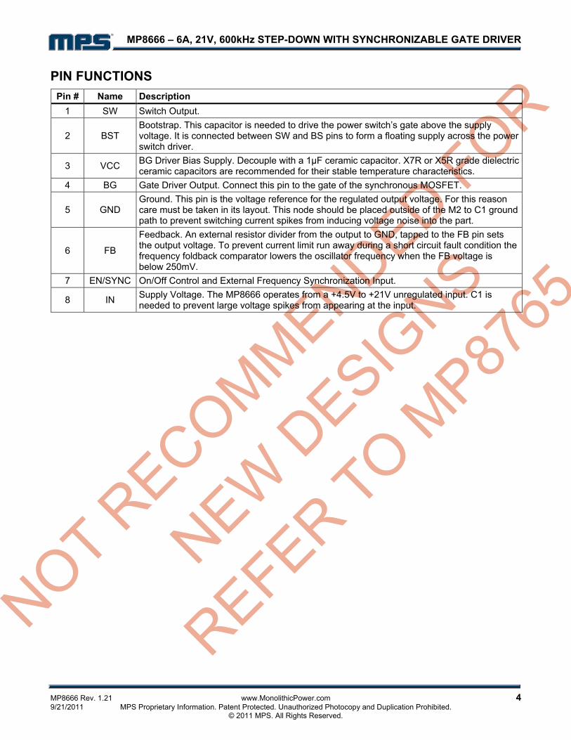
PIN FUNCTIONS Pin # Name Description
1 SW Switch Output.
2 BST Bootstrap. This capacitor is needed to drive the power switch’s gate above the supply voltage. It is connected between SW and BS pins to form a floating supply across the power switch driver.
3 VCC BG Driver Bias Supply. Decouple with a 1µF ceramic capacitor. X7R or X5R grade dielectric ceramic capacitors are recommended for their stable temperature characteristics.
4 BG Gate Driver Output. Connect this pin to the gate of the synchronous MOSFET.
5 GND Ground. This pin is the voltage reference for the regulated output voltage. For this reason care must be taken in its layout. This node should be placed outside of the M2 to C1 ground path to prevent switching current spikes from inducing voltage noise into the part.
6 FB
Feedback. An external resistor divider from the output to GND, tapped to the FB pin sets the output voltage. To prevent current limit run away during a short circuit fault condition the frequency foldback comparator lowers the oscillator frequency when the FB voltage is below 250mV.
7 EN/SYNC On/Off Control and External Frequency Synchronization Input.
8 IN Supply Voltage. The MP8666 operates from a +4.5V to +21V unregulated input. C1 is needed to prevent large voltage spikes from appearing at the input.

MP8666 – 6A, 21V, 600kHz STEP-DOWN WITH SYNCHRONIZABLE GATE DRIVER
MP8666 Rev. 1.21 www.MonolithicPower.com 5 9/21/2011 MPS Proprietary Information. Patent Protected. Unauthorized Photocopy and Duplication Prohibited. © 2011 MPS. All Rights Reserved.
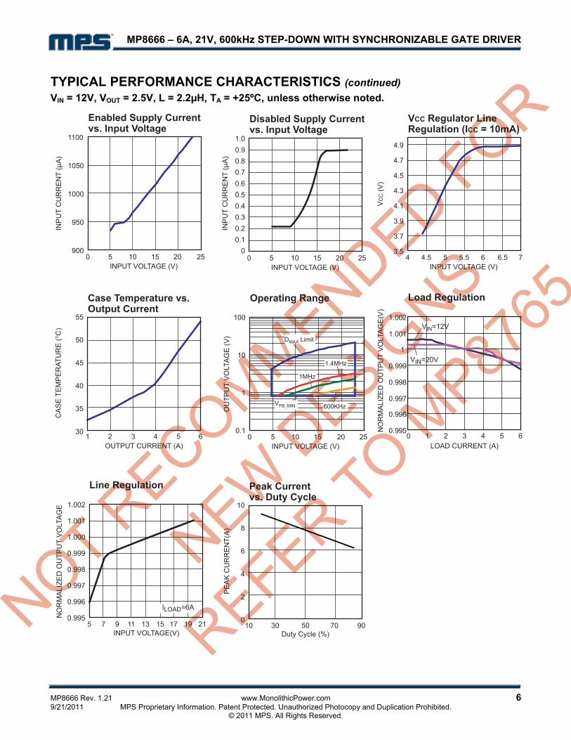
TYPICAL PERFORMANCE CHARACTERISTICS VIN = 12V, VOUT = 2.5V, L = 2.2µH, TA = +25ºC, unless otherwise noted.
MP8666 – 6A, 21V, 600kHz STEP-DOWN WITH SYNCHRONIZABLE GATE DRIVER
MP8666 Rev. 1.21 www.MonolithicPower.com 6 9/21/2011 MPS Proprietary Information. Patent Protected. Unauthorized Photocopy and Duplication Prohibited. © 2011 MPS. All Rights Reserved.
TYPICAL PERFORMANCE CHARACTERISTICS (continued) VIN = 12V, VOUT = 2.5V, L = 2.2µH, TA = +25ºC, unless otherwise noted.
Enabled Supply Current vs. Input Voltage
1100
1050
1000
950
9000 5 10 15 20 25
INPUT VOLTAGE (V)
55
50
45
40
35
30
CA
SE
TEM
PE
RAT
UR
E (O
C)
1 2 3 4 65OUTPUT CURRENT (A)
100
10
1
0.1
OU
TPU
T V
OLT
AG
E (V
)
0 5 10 15 20 25INPUT VOLTAGE (V)
NO
RM
ALI
ZED
OU
TPU
T V
OLT
AG
E(V
)
LOAD CURRENT (A)
Case Temperature vs. Output Current
10
8
6
4
2
0
PE
AK
CU
RR
EN
T(A
)
10 7030 9050Duty Cycle (%)
Peak Current vs. Duty Cycle
Operating Range
Disabled Supply Currentvs. Input Voltage
1.00.90.80.70.60.50.40.30.20.1
00 5 10 15 20 25
INPUT VOLTAGE (V)
VCC Regulator Line Regulation (ICC = 10mA)
4.9
4.7
4.5
4.3
4.1
3.9
3.7
3.5
VC
C (V
)
4 54.5 5.5 6 6.5 7INPUT VOLTAGE (V)
VIN=12V
VIN=20V
Load Regulation
1.002
1.001
1.000
0.999
0.998
0.997
0.996
0.995NO
RM
ALI
ZED
OU
TPU
T V
OLT
AG
E
5 7 9 13 1911 15 17 21
ILOAD=6A
Line Regulation
1MHz
1.4MHz
600KHzVFB_MIN
DMAX Limit
0.995
0.996
0.997
0.998
0.999
1
1.001
1.002
0 1 2 3 4 5 6
INPUT VOLTAGE(V)

MP8666 – 6A, 21V, 600kHz STEP-DOWN WITH SYNCHRONIZABLE GATE DRIVER
MP8666 Rev. 1.21 www.MonolithicPower.com 7 9/21/2011 MPS Proprietary Information. Patent Protected. Unauthorized Photocopy and Duplication Prohibited. © 2011 MPS. All Rights Reserved.
OPERATION
IN
EN/SYNC
FB
SW
VCC
BG
GND
BST
REGULATOR OSCILLATOR600KHz DRIVER
CURRENT SENSEAMPLIFIER
ERRORAMPLIFIER
COMP
CURRENTLIMITCOMPARATOR
PWMCOMPARATOR
DRIVER
D1
REGULATOR
REFERENCE
Σ
--+ --
+
--+
S
R
R
Q
Q
--+
54pF
1pFVCC
VCC
Figure 1—Functional Block Diagram The MP8666 is a fixed frequency, synchronous, step-down switching regulator with an integrated high-side power MOSFET and a gate driver for a low-side external MOSFET. It achieves 6A continuous output current over a wide input supply range with excellent load and line regulation. It provides a single highly efficient solution with current mode control for fast loop response and easy compensation.
The MP8666 operates in a fixed frequency, peak current control mode to regulate the output voltage. A PWM cycle is initiated by the internal clock. The integrated high-side power MOSFET is turned on and remains on until its current reaches the value set by the COMP voltage. When the power switch is off, it remains off until the next clock cycle starts. If, in 90% of one PWM period, the current in the power MOSFET does not reach the COMP set current value, the power MOSFET will be forced to turn off.
Error Amplifier The error amplifier compares the FB pin voltage with the internal 0.8V reference (REF) and outputs a current proportional to the difference between the two. This output current is then used to charge or discharge the internal compensation network to form the COMP voltage, which is used to control the power MOSFET current. The optimized internal compensation network minimizes the external component counts and simplifies the control loop design.
Internal Regulator Most of the internal circuitries are powered from the 5V internal regulator. This regulator takes the VIN input and operates in the full VIN range. When VIN is greater than 5.0V, the output of the regulator is in full regulation. When VIN is lower than 5.0V, the output decreases. Since this internal regulator provides the bias current for the bottom gate driver that requires significant amount of current depending upon the external MOSFET selection, a 1µF ceramic capacitor for decoupling purpose is required.
MP8666 – 6A, 21V, 600kHz STEP-DOWN WITH SYNCHRONIZABLE GATE DRIVER
MP8666 Rev. 1.21 www.MonolithicPower.com 8 9/21/2011 MPS Proprietary Information. Patent Protected. Unauthorized Photocopy and Duplication Prohibited. © 2011 MPS. All Rights Reserved.
Enable/Synch Control The MP8666 has a dedicated Enable/Synch control pin (EN/SYNC). By pulling it high or low, the IC can be enabled and disabled by EN. Tie EN to VIN for automatic start up. To disable the part, EN must be pulled low for at least 5µs.
The MP8666 can be synchronized to external clock range from 300KHz up to 1.5MHz through the EN/SYNC pin. The internal clock rising edge is synchronized to the external clock rising edge.
Under-Voltage Lockout (UVLO) Under-voltage lockout (UVLO) is implemented to protect the chip from operating at insufficient supply voltage. The MP8666 UVLO comparator monitors the output voltage of the internal regulator, VCC. The UVLO rising threshold is about 4.0V while its falling threshold is a consistent 3.2V.
Internal Soft-Start The soft-start is implemented to prevent the converter output voltage from overshooting during startup. When the chip starts, the internal circuitry generates a soft-start voltage (SS) ramping up from 0V to 1.2V. When it is lower than the internal reference (REF), SS overrides REF so the error amplifier uses SS as the reference. When SS is higher than REF, REF regains control.
Over-Current-Protection and Hiccup The MP8666 has cycle-by-cycle over current limit when the inductor current peak value exceeds the set current limit threshold. Meanwhile, output voltage starts to drop until FB is below the Under-Voltage (UV) threshold, typically 30% below the reference. Once a UV is triggered, the MP8666 enters hiccup mode to periodically restart the part. This protection mode is especially useful when the output is dead-short to ground. The average short circuit current is greatly reduced to alleviate the thermal issue and to protect the regulator. The MP8666 exits the hiccup mode once the over current condition is removed.
Thermal Shutdown Thermal shutdown is implemented to prevent the chip from operating at exceedingly high temperatures. When the silicon die temperature is higher than 150°C, it shuts down the whole chip. When the temperature is lower than its lower threshold, typically 140°C, the chip is enabled again.
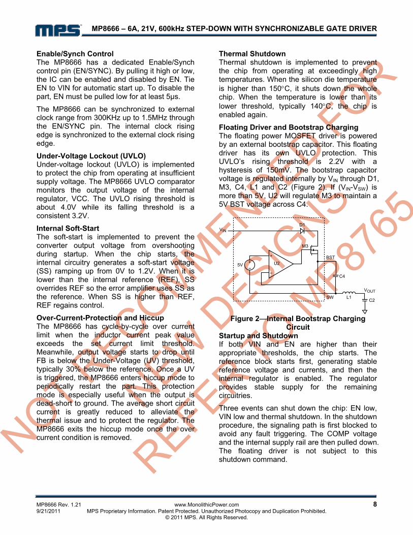
Floating Driver and Bootstrap Charging The floating power MOSFET driver is powered by an external bootstrap capacitor. This floating driver has its own UVLO protection. This UVLO’s rising threshold is 2.2V with a hysteresis of 150mV. The bootstrap capacitor voltage is regulated internally by VIN through D1, M3, C4, L1 and C2 (Figure 2). If (VIN-VSW) is more than 5V, U2 will regulate M3 to maintain a 5V BST voltage across C4.
--
+
--+
VIN
5V U2
D1
M3
BST
SW
C4
C2L1
VOUT
Figure 2—Internal Bootstrap Charging
Circuit Startup and Shutdown If both VIN and EN are higher than their appropriate thresholds, the chip starts. The reference block starts first, generating stable reference voltage and currents, and then the internal regulator is enabled. The regulator provides stable supply for the remaining circuitries.
Three events can shut down the chip: EN low, VIN low and thermal shutdown. In the shutdown procedure, the signaling path is first blocked to avoid any fault triggering. The COMP voltage and the internal supply rail are then pulled down. The floating driver is not subject to this shutdown command.

MP8666 – 6A, 21V, 600kHz STEP-DOWN WITH SYNCHRONIZABLE GATE DRIVER
MP8666 Rev. 1.21 www.MonolithicPower.com 9 9/21/2011 MPS Proprietary Information. Patent Protected. Unauthorized Photocopy and Duplication Prohibited. © 2011 MPS. All Rights Reserved.
APPLICATION INFORMATION The schematic on the front page shows a typical MP8666 application. The IC can provide up to 6A output current at a nominal output voltage of 3.3V. For proper thermal performance, the exposed pad of the device must be soldered down to the printed circuit board.
Setting the Output Voltage The external resistor divider is used to set the output voltage (see the schematic on front page). The feedback resistor R1 also sets the feedback loop bandwidth with the internal compensation capacitor (see Figure 1). Choose R1 to be around 40.2kΩ for optimal transient response. R2 is then given by:
OUT
R1R2 V 10.808V
=−
Table 1—Resistor Selection for Common Output Voltages
VOUT (V) R1 (kΩ) R2 (kΩ) 1.8 40.2 (1%) 32.4 (1%) 2.5 40.2 (1%) 19.1 (1%) 3.3 40.2 (1%) 13 (1%) 5 40.2 (1%) 7.68 (1%)
Selecting the Inductor A 1µH to 10µH inductor with a DC current rating of at least 25% percent higher than the maximum load current is recommended for most applications. For highest efficiency, the inductor DC resistance should be less than 15mΩ. For most designs, the inductance value can be derived from the following equation.
OSCLIN
OUTINOUT
fIV)VV(V
L×Δ×−×
=
Where ΔIL is the inductor ripple current.
Choose inductor current to be approximately 30% of the maximum load current, 6A. The maximum inductor peak current is:
2I
II LLOAD)MAX(L
Δ+=
Under light load conditions below 100mA, larger inductance is recommended for improved efficiency.
Synchronous MOSFET The external synchronous MOSFET is used to supply current to the inductor when the internal high-side switch is off. It significantly reduces the power loss when compared against a Schottky rectifier.
Table 2 lists example synchronous MOSFETs and manufacturers.
Table 2—Synchronous MOSFET Selection Guide
Part No. Manufacture FDS6670AS Fairchild
IRF7821 International Rectifier AM4874 Analog Power
Selecting the Input Capacitor The input capacitor (C1) reduces the surge current drawn from the input and the switching noise from the device. The input capacitor impedance at the switching frequency should be less than the input source impedance to prevent high frequency switching current from passing to the input. Ceramic capacitors with X5R or X7R dielectrics are highly recommended because of their low ESR and small temperature coefficients. For 6A output applications, a 22µF capacitor is sufficient.
Selecting the Output Capacitor The output capacitor (C2) keeps output voltage small and ensures regulation loop stability. The output capacitor impedance should be low at the switching frequency. Ceramic capacitors with X5R or X7R dielectrics are recommended.

MP8666 – 6A, 21V, 600kHz STEP-DOWN WITH SYNCHRONIZABLE GATE DRIVER
MP8666 Rev. 1.21 www.MonolithicPower.com 10 9/21/2011 MPS Proprietary Information. Patent Protected. Unauthorized Photocopy and Duplication Prohibited. © 2011 MPS. All Rights Reserved.
PCB Layout Guide PCB layout is very important to achieve stable operation. Please follow these guidelines and take Figure3 for references.
1) Keep the path of switching current short and minimize the loop area formed by Input cap, high-side and low-side MOSFETs.
2) Keep the connection of low-side MOSFET between SW pin and input power ground as short and wide as possible.
3) Ensure all feedback connections are short and direct. Place the feedback resistors and compensation components as close to the chip as possible.
4) Route SW away from sensitive analog areas such as FB.
5) Connect IN, SW, and especially GND respectively to a large copper area to cool the chip to improve thermal performance and long-term reliability.
R3
LGATE
VCC
BST
SWIN
EN
FB
C1
Cb
Rb
R1
C2
L1
PGND
87
65 4
32
1
SGND
8 7 6 5
4321
GNDR2
C3
Top Layer
SGND
Bottom Layer
Figure 3—PCB Layout External Bootstrap Diode An external bootstrap diode may enhance the efficiency of the regulator, the applicable conditions of external BST diode is:
Duty cycle is high: D=IN
OUT
VV >65%
In these cases, an external BST diode is recommended from the output of the voltage regulator to BST pin, as shown in Fig.4
MP8666SW
BST C
L
BST
COUT
External BST DiodeIN4148
VCC
Figure 4—Add Optional External Bootstrap
Diode to Enhance Efficiency The recommended external BST diode is IN4148, and the BST cap is 0.1~1µF.

MP8666 – 6A, 21V, 600kHz STEP-DOWN WITH SYNCHRONIZABLE GATE DRIVER
NOTICE: The information in this document is subject to change without notice. Users should warrant and guarantee that third party Intellectual Property rights are not infringed upon when integrating MPS products into any application. MPS will not assume any legal responsibility for any said applications.
MP8666 Rev. 1.21 www.MonolithicPower.com 11 9/21/2011 MPS Proprietary Information. Patent Protected. Unauthorized Photocopy and Duplication Prohibited. © 2011 MPS. All Rights Reserved.
PACKAGE INFORMATION
SOIC8E (EXPOSED PAD)
SEE DETAIL "A"
0.0075(0.19)0.0098(0.25)
0.050(1.27)BSC
0.013(0.33)0.020(0.51)
SEATING PLANE0.000(0.00)0.006(0.15)
0.051(1.30)0.067(1.70)
TOP VIEW
FRONT VIEW
SIDE VIEW
BOTTOM VIEW
NOTE:
1) CONTROL DIMENSION IS IN INCHES. DIMENSION IN BRACKET IS IN MILLIMETERS. 2) PACKAGE LENGTH DOES NOT INCLUDE MOLD FLASH, PROTRUSIONS OR GATE BURRS. 3) PACKAGE WIDTH DOES NOT INCLUDE INTERLEAD FLASH OR PROTRUSIONS. 4) LEAD COPLANARITY (BOTTOM OF LEADS AFTER FORMING) SHALL BE 0.004" INCHES MAX. 5) DRAWING CONFORMS TO JEDEC MS-012, VARIATION BA. 6) DRAWING IS NOT TO SCALE.
0.089(2.26)0.101(2.56)
0.124(3.15)0.136(3.45)
RECOMMENDED LAND PATTERN
0.213(5.40)
0.063(1.60)
0.050(1.27)0.024(0.61)
0.103(2.62)
0.138(3.51)
0.150(3.80)0.157(4.00)PIN 1 ID
0.189(4.80)0.197(5.00)
0.228(5.80)0.244(6.20)
1 4
8 5
0.016(0.41)0.050(1.27)0o-8o
DETAIL "A"
0.010(0.25)0.020(0.50) x 45o
0.010(0.25) BSCGAUGE PLANE
Mouser Electronics
Authorized Distributor
Click to View Pricing, Inventory, Delivery & Lifecycle Information: Monolithic Power Systems (MPS):
MP8666DN-LF MP8666DN-LF-Z