mosfet modeling aimed at minimizing emi in...
TRANSCRIPT

THESIS FOR THE DEGREE OF LICENTIATE OF ENGINEERING
MOSFET Modeling Aimed at Minimizing EMI inSwitched DC/DC Converters Using Active Gate Control
ANDREAS KARVONEN
Department of Energy and EnvironmentDivision of Electric Power Engineering
CHALMERS UNIVERSITY OF TECHNOLOGYGoteborg, Sweden 2009

MOSFET Modeling Aimed at Minimizing EMI in Switched DC/DC Converters UsingActive Gate ControlANDREAS KARVONEN
c© ANDREAS KARVONEN, 2009.
Licentiante Thesis at the Graduate School in Energy and Environment
Department of Energy and EnvironmentDivision of Electric Power EngineeringChalmers University of TechnologySE–412 96 GoteborgSwedenTelephone +46 (0)31–772 1000
Chalmers Bibliotek, ReproserviceGoteborg, Sweden 2009

To all of those who believed...

iv
MOSFET Modeling Aimed at Minimizing EMI in Switched DC/DC Converters UsingActive Gate ControlANDREAS KARVONENDepartment of Energy and EnvironmentChalmers University of Technology
Abstract
This thesis deals with electromagnetic interference that can arise from switched DC/DC-converters intended for low-power applications, e.g. within the telecom or automotiveindustry. It analyzes measures and methods that can appliedwhen a reduction of EMIdirectly at the source without using any additional means such as shielding and filteringis desired. By investigating the physical properties of thetwo most important ingoingcomponents, the diode and the MOSFET, an improved MOSFET model and a new gatevoltage control method is proposed. This method is referredto as active gate control witha operating principle where a controller circuit shapes thedesired output to a sinusoidaltrajectory during the entire switching event. By doing this, it is shown that the harmoniccontent in the output signal can be reduced. The proposed MOSFET model is used as abase for extracting suitable controller parameters with the help of a linearized state-spacesystem. Two different outputs were selected and investigated, either the drain-source volt-age or the drain current. The general conclusion from simulations and measurements arethat active gate control where the drain current is selectedas the controlled quantity hasgood potential for reducing the harmonics and the emitted electromagnetic disturbancein a switched DC/DC converter even though it sets high demands on the controller cir-cuit. The analysis shows that a controller with static parameters derived on basis of theproposed MOSFET model is not sufficient due to the complexityof the system whichincludes many nonlinearities and varying parameters. In order to obtain better transitionsthat are valid over a wider range of operating points, adaptive control needs to be imple-mented. Simulations shows that by carefully selecting the controller parameters based onthe proposed MOSFET model and adapting the parameters to thecurrent operating pointan improvement in performance and robustness can be achieved.
Index Terms: Electromagnetic compatibility, Electromagnetic interference, DC-DCpower conversion, Semiconductor device measurements, Semiconductor devicemodeling, MOSFET switches, Power semiconductor diodes, Adaptive control, Statespace methods.
v

vi

Acknowledgements
The financial support given by Volvocars AB, SAAB Microwave Systems, Ericsson, SKFand Vinnova is gratefully acknowledged. I would also like tothank all members in theproject group, Bjorn Bergqvist who has been the project leader, Johan Falt, Anders Frickand Goran Lindsten. A special thank is directed to Trygve Tuveson who initiated theproject and kept coming with new ideas throughout the project. Also, thanks to PierreGildert who supported me when starting this thesis and Henrik Holst whose experimentshave taken me far.
At the department I would like to thank my supervisor Torbjorn Thiringer who alwaysfind some extra time for discussions, no matter the time and reason. My supportive col-leagues are gratefully acknowledged; Stefan Lundberg for constructive discussions, Mas-simo Bongiorno for techincal support and Julia Paixao for the article. A special thank toJohanAstrom who always listen to my reflections and contribute with new creative ideas.
Thanks to Kristofer Andersson at the Microwave ElectronicsLaboratory on Chalmers forhelping me with the equipment. The enlightenment from Professor Claes Breitholtz ishighly appreciated; the words shall act as a commandment forall coming work. Thanksto all Master Thesis workers that have contributed, especially Niklas Fransson and GustavJohanneson for their good spirit and valuable results.
At least but not last, the most important support; my friendsand my family. A warm thankto all of you that have supported, hugged and encouraged whendisbelief have struck.Without you this would not have been possible.
Andreas KarvonenGoteborg, SwedenSpring, 2009
vii

viii

Contents
Abstract v
Acknowledgements vii
Contents ix
1 Introduction 11.1 Problem Background . . . . . . . . . . . . . . . . . . . . . . . . . . . . 11.2 Objectives and Scope of Thesis . . . . . . . . . . . . . . . . . . . . . .. 31.3 Contributions with Present Work . . . . . . . . . . . . . . . . . . . .. . 3
1.3.1 MOSFET Modeling . . . . . . . . . . . . . . . . . . . . . . . . 31.3.2 Active Gate Control . . . . . . . . . . . . . . . . . . . . . . . . 31.3.3 Double MOSFET Switching . . . . . . . . . . . . . . . . . . . . 4
1.4 Outline of Thesis . . . . . . . . . . . . . . . . . . . . . . . . . . . . . . 41.5 Publications . . . . . . . . . . . . . . . . . . . . . . . . . . . . . . . . . 4
2 Semiconductors and Converters 72.1 Component Background . . . . . . . . . . . . . . . . . . . . . . . . . . 72.2 The pn-Diode . . . . . . . . . . . . . . . . . . . . . . . . . . . . . . . . 7
2.2.1 Modeling of the pn-Diode . . . . . . . . . . . . . . . . . . . . . 92.3 The Schottky Diode . . . . . . . . . . . . . . . . . . . . . . . . . . . . . 142.4 The PiN-Diode . . . . . . . . . . . . . . . . . . . . . . . . . . . . . . . 15
2.4.1 Conductivity Modulation and On-State Losses . . . . . . .. . . 152.4.2 Turn-on Behavior of the PiN-Diode . . . . . . . . . . . . . . . . 162.4.3 Turn-off Behavior of the PiN-Diode . . . . . . . . . . . . . . . .162.4.4 PiN Diode Modeling . . . . . . . . . . . . . . . . . . . . . . . . 19
2.5 The MOSFET . . . . . . . . . . . . . . . . . . . . . . . . . . . . . . . . 202.5.1 Operating Regions for the Power MOSFET . . . . . . . . . . . . 212.5.2 Internal Capacitances of the MOSFET . . . . . . . . . . . . . . .232.5.3 The MOSFET in conducting State . . . . . . . . . . . . . . . . . 242.5.4 Turn-On Behavior of the MOSFET . . . . . . . . . . . . . . . . 262.5.5 Turn-Off Behavior of the MOSFET . . . . . . . . . . . . . . . . 28
ix

Contents
2.5.6 The MOSFET model in SPICE . . . . . . . . . . . . . . . . . . 302.5.7 PSPICE MOSFET Models Adapted for Switching Applications . 31
2.6 EMI Generated by Switched DC/DC Converters . . . . . . . . . . .. . . 332.6.1 Hard Switching Converters . . . . . . . . . . . . . . . . . . . . . 332.6.2 Simulating EMI from a Switched DC/DC Converter . . . . . .. 362.6.3 Random Switching . . . . . . . . . . . . . . . . . . . . . . . . . 372.6.4 Gate Voltage Control . . . . . . . . . . . . . . . . . . . . . . . . 40
3 Semiconductor Modeling 433.1 Nodal Analysis Vs. State Variable Approach . . . . . . . . . . .. . . . . 433.2 Improving and verifying the diode model . . . . . . . . . . . . . .. . . 45
3.2.1 Determining thepn-Junction Capacitance . . . . . . . . . . . . . 453.2.2 Validation of the Reverse Recovery . . . . . . . . . . . . . . . .473.2.3 Implementation of a Diode Model Based on Charge Locations . . 50
3.3 A Novel MOSFET Model Based on Circuit Analysis . . . . . . . . .. . 513.3.1 Parameter Extraction for a Power MOSFET . . . . . . . . . . . .533.3.2 MOSFET Model Under Static Conditions . . . . . . . . . . . . . 553.3.3 MOSFET Model Under Dynamic Conditions . . . . . . . . . . . 613.3.4 Switching With Purely Resistive Load . . . . . . . . . . . . . .. 703.3.5 Comparison of Simulations and Measurements . . . . . . . .. . 71
4 Active Gate Control and Controller Design 754.1 Active Gate Control - Theoretical Derivation . . . . . . . . .. . . . . . . 754.2 Controller Design . . . . . . . . . . . . . . . . . . . . . . . . . . . . . . 784.3 Selecting the output of the system . . . . . . . . . . . . . . . . . . .. . 834.4 Controller Design . . . . . . . . . . . . . . . . . . . . . . . . . . . . . . 88
5 Implementation of Active Gate Control 915.1 Step Response of the System . . . . . . . . . . . . . . . . . . . . . . . . 935.2 Sinusoidal Step Response of the System . . . . . . . . . . . . . . .. . . 985.3 Controller Design With Varying Parameters . . . . . . . . . . .. . . . . 1015.4 Robustness of the Circuit . . . . . . . . . . . . . . . . . . . . . . . . . .1085.5 Switching Losses with Active Gate Control . . . . . . . . . . . .. . . . 109
6 Conclusions 113
7 Future Work 115
Written References 117
Internet References 124
x

Contents
A Symbols and Glossary 127
B Derivations of Essential Formulas 131
C Selected Publications 137
xi

Contents
xii

Chapter 1
Introduction
1.1 Problem Background
Power electronic converters can be found wherever there is aneed to modify the electricalenergy form (i.e. to modify its voltage, current or frequency). Power electronics are usedin widely different areas such as point-of-load supplies oncomputer motherboards, trac-tion control for electric drives and connection of windpower-plants to the grid. Therefore,their power range from some milliwatts to hundreds of megawatts. This thesis focuseson the usage of low power DC/DC converters intended for onboard power. Modern elec-tronic devices, e.g. processors, often make use of several different voltage levels in thesame application which gives a demand of power electronics.
One trend in e.g. the automotive industry is that objects that originally were mechani-cally operated are being replaced by electronically controlled ones. These electrical loadsoften demands variable power at a varying voltage level, hence DC/DC converters andDC/DC inverters are employed. Examples of such applications using switching powersupplies in vehicles are fuel pumps, seat heaters and beam lights. The trend of employ-ing several switched converters can also be applied to the server and telecom industry,not due to the plentiful occurrence of mechanical loads, butrather to the high demandof multiple voltages that supplies processors and other consumers. Another aspect thatemphasizes the importance of reduced electromagnetic interference from switched con-verters is the aspect of area and volume. In the automotive industry, all locations whereelectronic equipment can be placed are strictly predetermined and can not be adjusted.This can also be applied to the telecom industry where switched converters can be placedclose to sensitive radio frequency equipment. Since the converter often carries high cur-rents and utilizes large magnetic and inductive components, it often acts as a source ofdisturbance.
The perhaps most important incitement for the increased concern of EMI is the relatively
1

Chapter 1. Introduction
new EMC Directive, 2004/108/EC, that is valid from July 2007within the entire EU. Itis by some considered as one of the most comprehensive standards ever to originate fromthe European Commission. The directive consists of a collection of regulations that ev-erything powered by electricity, regardless of the power source, has to fulfil before theproduct can be marketed in the EU. The EMC Directive consistsof mainly two areas. Onone hand it governs the electromagnetic emissions of equipment in order to ensure that,in its intended use, the equipment does not disturb radio andtelecommunication or otherequipment. On the other hand, the Directive also governs theimmunity of equipment tointerference and seeks to ensure that the equipment is not disturbed by radio emissionsnormally present in the surroundings. The most commonly adapted standards originatefrom Comite International Special des Perturbations Radioelectriques (CISPR) which isa part of IEC. These standards cover several different areasand the specific standard thatapply to a certain product is often adapted directly by the manufacturer to facilitate com-pliance with the EMC Directive. An example is CISPR 25 (Vehicles, boats and internalcombustion engines - Radio disturbance characteristics - Limits and methods of measure-ment for the protection of on-board receivers) which is usedby several large automotivecompanies [65].
As a part of the growing concern of electromagnetic fields theEuropean parliament havepublished directive 2004/40/EC which aims at protecting workers from adverse healtheffects resulting from exposure to non ionizing electromagnetic fields. The directive con-tains minimum requirements concerning electromagnetic fields which employers in themember states of the European Union must fulfil 30th of April 2012. An example of anarea of application is a car which is considered an working environment for many, thusshall directive 2004/40/EC be applied. This gives the need for the automotive industryto carefully interpret and take the appropriate measures necessary to follow this directive[1]. All in all, these new directives in combination with thegrowing electrification andincrease of converter power density are the major reason forinvestigating new methodsthat can minimize EMI from switched DC/DC converters.
One of the most widespread semiconductor models used for simulation of analog cir-cuitry is the SPICE model developed at Berkeley in the mid 1960’s. Since the relativelyrecent introduction of semiconductors with a high voltage handling capability, and thewidespread usage of switched power converters and electricdrives, the use of SPICE as amodeling language can be considered to be insufficient. Thisis mainly due to deficits inthe original semiconductor models that are not adapted to new structures and propertiespresent in modern power semiconductors, but also due to the complex nature of switchedDC/DC converters.
2

1.2. Objectives and Scope of Thesis
1.2 Objectives and Scope of Thesis
Accordingly, it would be useful to develop a simplified powerMOSFET model suited forswitched power applications that can be used for determination of voltage and currentwaveforms during a switching event. The model shall be sufficiently accurate to be ableto give a rough estimation of the EMI. Moreover, it would be very useful if the simplifiedmodel can be used for designing a controller adapted for active gate control. By control-ling the gate of a MOSFET, more EMI-friendly currents and voltages can be obtained.
The usage and implementation of many earlier developed models, can in some cases bevery complex, require long simulation and have a complicated procedure of parameterextraction. In view of this, the objective of this thesis is to obtain a simple model and toverify the results to the greatest extent possible. The models proposed and evaluated in thethesis is designed with simplicity as the main cornerstone.In the section below follows alist of contributions that this thesis comprise of.
1.3 Contributions with Present Work
1.3.1 MOSFET Modeling
A simple system consisting of a MOSFET as a switching elementand a resistive loadwas implemented as a state-space model. This system, including the newly derived MOS-FET model with particular focus on the nonlinear internal capacitors, was used to derivecontroller parameters intended for active gate control.
• A simplified model of MOSFET’s adapted for switching applications.
• The validity of the model is investigated with focus put the usage of the model as ahelp for circuit analysis and controller design.
1.3.2 Active Gate Control
Active gate control reduces the high frequency contents in apulsed signal by applyingsmooth transitions. This part of the thesis is based on a previously performed work per-formed by Henrik Holst and Pravin Futane at Chalmers University of Technology, see [2].The contributions with this thesis are:
• Better digital generation of a sinusoidal waveform that acts as a reference for thecontroller circuit.
• Controller design based on an analytical approach.
3

Chapter 1. Introduction
• Problems that comes with a variable supply voltage are handled by controlling thedrain current instead.
• Implementation of an adaptive controller structure with parameters based on theproposed MOSFET model in the simulation environment.
1.3.3 Double MOSFET Switching
The principle of double MOSFET switching was investigated at an early stage of thethesis. The final result was however slightly out of scope forthe final conclusions, theresults are consequently presented in Appendix C.
1.4 Outline of Thesis
Chapter 2 of the thesis acts as a background and covers the physical properties and de factostandard models of diodes and MOSFET’s as well as how EMI is generated in switchedDC/DC converters together with methods for reduction.
Chapter 3 investigates the deficits of the de facto standard models presented in Chapter 2.The physical and electrical properties of MOSFET’s are measured and act as a base for ora new type of MOSFET model. The model is verified, simulationsas well as measurementresults are presented.
Chapter 4 introduces the concept of active gate control and how the previously derivedMOSFET model can act as a base of parameter derivations. Thischapter also discussesstate space modeling, linearization of the system and how different methods can be usedwhen designing a suitable controller.
In Chapter 5 the theory covering active gate control is realized. Simulation and measure-ment results are presented and from the results conclusionsare drawn.
1.5 Publications
The publications originating from this licentiate projectcan be found in Appendix C andare summarized below.
I J. Paixao,A. Karvonen, J. Astrom, T. Tuveson, and T. Thiringer, ”EMI Reduc-tion Using Symmetrical Switching and Capacitor Control” published at2008 Asia-Pacific Symposium on Electromagnetic Compatibility in conjunction with the 19thIntern. Zurich Symposium on Electromagnetic Compatibility, Singapore, 2008.
4

1.5. Publications
II A. Karvonen, H. Holst, T. Tuveson, T. Thiringer, and P. Futane, ”Reduction of EMIin Switched Mode Converters by Shaped Pulse Transitions” published atSAE WorldConference 2007. Detroit, Michigan, USA. Copyright SAE International, 2007.
5

Chapter 1. Introduction
6

Chapter 2
Semiconductors and Converters
2.1 Component Background
Semiconductor devices with current ratings over 1A are usually referred to as power semi-conductors. The most significant properties of these devices are their ability to handlelarge currents and high voltages. Blocking voltages of suchdevices range from a fewvolts up to 10kV and the current handling may range up to several thousands of amperes.One property that many of these devices have in common, is theuse of silicon as semi-conducting material. Silicon is a material with well known material properties and it isused in a wide range of areas. The manufacturing process has been refined during the lastdecades which have resulted in a large number of manufactured silicon devices with verylow production costs. However, silicon has a considerable deficit when large powers areto be handled; the breakdown field strength of the material requires a considerable waferthickness in order to achieve sufficient voltage handling capability. Since the thickness ofthe semiconducting material is the most important factor that contributes to the overalllosses in the device, the possibility to use a thin wafer would strongly evolve power semi-conductors even further. Recent research has showed that new materials such as siliconcarbide (SiC), gallium nitride (GaN) and diamond (C) has substantially improved mate-rial properties in relation to silicon. Due to the early stage in the development of thesematerials, several problems must still be mastered; SiC, which might be one of the mostpromising new materials, faces problems with cost-effective production of high-qualitySiC wafers [3]. At the time of printing this thesis, silicon is still the main material used inpower semiconductors. Hence, this thesis only focuses on silicon devices and their usage.
2.2 The pn-Diode
The pn-junction is undoubtedly the most important buildingblock in the majority of mod-ern electronics. Most semiconductor devices are made of some kind of pn-junction, thus
7

Chapter 2. Semiconductors and Converters
a thorough understanding of its physical properties is necessary for deeper understandingof more complex devices such as diodes and transistors. Whena p-doped material and ann-doped material is brought together, excess electrons in the n-doped material will diffuseinto the p-doped material. Equilibrium will be reached where the electric field due to thebuilt up net charge balances the diffusion of electrons toward the p-region. The electricfield also gives rise to a potential drop across the two regions, which often is referred toas the built in voltage (Vbi) of a pn-junction [3].
Two of the most important mechanisms that can not be neglected are the generation andrecombination processes in the depletion layer and the avalanche breakdown of a reversebiased junction. In a reverse biased pn-junction, no current can flow through the junctiondue to the reverse bias. However there still exits a depletion layer with an electric fieldin which a net generation of electron-hole pairs will be existing. The freshly generatedelectron-hole pair is immediately separated due to the influence of the electric field, i.e. areverse current will flow. Applied external voltages greater than the built in voltage givesa reverse bias current density that approximately increases proportionally to the squareroot of the applied voltage [3]. Since the reverse current flowing through the pn-junctionis dependant on the carrier generation rate, the reverse current shows a temperature depen-dence. As the temperature of the device increases, the reverse current will also increase[4].
If the pn-junction is forward biased, the same discussion can be applied as for the re-verse biased junction. The applied external voltage gives rise to a depletion region thatdecreases in width as the voltage increases. For low values of the forward voltage (VF ),the recombination is dominant. At higher values of the applied forward voltage, the cur-rent through the pn-junction predominantly consists of a diffusion component. The totalcurrent through the diode also shows a strong temperature dependant, i.e. if the temper-ature increases both the recombination current and the diffusion current increases. Therecombination current increases due to increased carrier lifetime and intrinsic carrier con-centration. The diffusion current increases due to temperature dependant diffusion coeffi-cients, increased carrier lifetime and increased carrier concentration [3].
Since electrons are moved within the crystal lattice both due to the influence of the appliedelectric field and due to the charge that is stored in the diodewhen it is forward biased,the diode can also be seen as a capacitor. In general, the total diode capacitance,CD,consists of two terms; the depletion capacitance (Cj) and the diffusion capacitance (Cd).The depletion capacitance originates from the accumulation of charges in the space chargeregion and its varying width. Linder [3] states that the depletion capacitance for a pn-junction varies according to
8

2.2. The pn-Diode
Cj(V ) =
√
εsqNDNA
2(ND + NA)(Vbi − Vapplied)(2.1)
Note that when the applied voltage (Vapplied) approaches the built in voltage (Vbi), thespace charge region becomes very thin which consequently gives a depletion capacitancethat goes toward infinity which also can be seen in Figure 2.1.
The diffusion capacitance depends on the gradient in the carrier concentration and theapplied voltage. If a change in the junction current is desired, the stored minority carriersclose to the space charge region must be removed. This can be resembled with a capacitorin which charges have to be moved. If these two mechanisms aresummed up and thetotal capacitance,CD, is plotted as a function of the applied voltage,VD, the total junctioncapacitance is shown in Figure 2.1.
C
VD
CD
Cj
Cd
Vbi
Fig. 2.1Total parasitic capacitance for a pn-junction diode.
The capacitance of a pn diode is frequently expressed as a function of the zero bias ca-pacitance,Cj(0), which is also term featured in the simulation language SPICE.
2.2.1 Modeling of the pn-Diode
The simplest semiconductor modeled in SPICE is thepn-junction diode. Originally, it isbased on the well known shockely equation
Idiode = IS
[
exp
(
VD
Vt
)
− 1
]
→ Idiode = IS
[
exp
(
qVD
kT
)
− 1
]
(2.2)
that describes the current through an ideal diode. In (2.2),IS is the saturation current(often referred to as the maximum reverse bias current),VD is the voltage over the diodeandVt is the thermal voltage. For adaptation to SPICE, an emissioncoefficient,N, isintroduced to model the ideality of the pn-junction. Also, aparallel conductance (GMIN)is inserted to help converge problems.
9

Chapter 2. Semiconductors and Converters
Idiode = IS
[
exp
(
− VD
N · Vt
)
− 1
]
+ VDGMIN (2.3)
The emission coefficient is an ideality factor that varies from 1 to 2. A higher emissioncoefficient indicates on a higher rate of recombination of carriers in the depletion layer.For a good diode,N equals 1. WhenVD is smaller than−5nVt, SPICE uses the assumptionthat the leakage current through the junction equals the reverse saturation current, henceis (2.3) simplified to
Idiode = −IS + VDGMIN. (2.4)
To model the breakdown voltage of the diode, the SPICE parameter BV is introduced.The current in the diode once the breakdown voltage has been reached is modeled withexponential behavior and can be expressed as
Idiode = −IS
[
exp
(
−BV + VD
Vt
)
− 1 +BV
Vt
]
. (2.5)
If these three equations are combined, the diode characteristics shown in Figure 2.2 isobtained.
VD
ExponentialBreakdown iD
VD=-5nVtVD=BV
Slope ofGMIN
Shockleyequation
GMIN
ID
Static DCdiode model
VD
Fig. 2.2Diode characteristics split into three regions (left) and the equivalent DC-circuit for thediode (right).
In addition to the current generator shown in Figure 2.2, a series resistance (RS) is oftenadded. The purpose of the resistance is to model the resistance in the connecting wires,the ohmic contact resistances and the ohmic drop in the quasineutral regions. This resis-tance causes a reduction in the internal diode voltage whichgives a decrease in the currentthrough the diode. This gives the need of a higher voltage to deliver the desired forwardcurrent (IF ) which results in higher power dissipation.
10

2.2. The pn-Diode
This model provides a good modeling of the entire static diode characteristics. How-ever, it has two major deficits; it does not take high level injection into considerationand it does not include any dynamic effects. High injection is a phenomena often foundin power semiconductors such as PiN-diodes and IGBTs. For the PiN-diode, numerousmore advanced models that takes high injection into consideration have been developed,see Section 2.4.4.
In order to obtain a better dynamic model designed for transient applications, eg. a switchedmode power supply, the diode capacitance is added to the model, see Figure 2.3.
GMIN
ID
V’D
RS
CD
VD
Fig. 2.3Diode large signal model with dynamic effects.
As the physical interpretation of the diode capacitance suggests,CD can be divided in twoparts; thediffusion capacitance, Cd, and thedepletion capacitance. SPICE interprets thedepletion capacitance as
Cj =Cj(0)
√
1 − Vapplied
Vbi
(2.6)
whereVapplied is the applied junction voltage,Cj(0) is the junction capacitance at zeroapplied bias (also known as the SPICE parameterCJ0) andVbi is the built-in voltagewhich equals the potential difference between thep-material and then-material at zerobias. The diffusion capacitance is according to Massobrio [5] modeled as
Cd =dQd
dV=
q
NkTTTISe
qVNkT (2.7)
whereN is the diode ideality coefficient found in Equation (2.3) andTT is a SPICE pa-rameter that describes the transit time for the carriers through the diode. The total junctioncapacitance,CD, can be calculated from the total stored charge and can consequently beexpressed as
11

Chapter 2. Semiconductors and Converters
CD =dQD
dV=
d(Qj + Qd)
dV(2.8)
Using the total stored charges, the total capacitance can bedefined as
V < FCVbi : CD =dQD
dV= TT
dID
dV+ CJ0
(
1 − V
Vbi
)
−m
(2.9)
V ≥ FCVbi : CD =dQD
dV= TT
dID
dV+
CJ0
F2
(
F3 −mV
Vbi
)
−m
(2.10)
whereF1, F2 andF3 are SPICE constants defined as
F1 =Vbi
1 − m
(
1 − (1 − FC)1−m)
(2.11)
F2 = (1 − FC)1−m (2.12)
F3 = 1 − FC (1 + m) (2.13)
To summarize, the SPICE model parameters for simulating large scale behavior consistsof five different parameters needed to describe the total capacitanceCD, namelyTT (Tran-sit time), CJ0 (Zero bias junction capacitance),M (Grading coefficient),VJ (built injunction potential) andFC (Coefficient for forward-bias depletion capacitance). Furtherreading can be found in [6, 7, 5].
For any type of pn-diode, the main operation principle is injection of minority carriersinto the depletion region that causes charge storage at the interface node located at theboundary between the the regions. For a practical pn-diode,the p-region is usually muchmore heavily doped than the n-region which usually is denoted by p+n. The fundamentalcharge control equation for a pn-junction diode which states that the diode current suppliesholes to the neutral n-region at the rate at which the stored charge increases plus the rateat which holes are being lost due to recombination. This relationship is usually termed asthe quasi-static model.
ID(t) =Qp
τ+
dQp
dt(2.14)
It has been shown by Tseng [8] that the excess carrier distribution profile in the vicinity ofthe pn-junction as the diode is being turned-off depends on the rate of change of the storedcharge. If a lowdQ/dt is present in the diode, the quasi-static charge equation isadequatesince the stored charge in the depletion region also becomesapproximately zero as thecharge in the node at the interface becomes zero. However, ifa highdQ/dt is present, asubstantial amount of stored charge still remains in the depletion region even though thecharge concentration at the interface has decreased to zero. It is this excess charge that
12

2.2. The pn-Diode
causes the behavior of the reverse recovery current. Chargestorage in the depletion layeris not modeled by SPICE, hence the sudden increase and snappybehavior of the diodecurrent at the moment when the charge node at the interface becomes depleted, see Figure2.4 for a comparison between SPICE and real behavior regarding the recovery current.Another deficit in SPICE is the lack of forward recovery modeling. Forward recovery isexplained in Section 2.4.2 and needs to be modeled by more complex models as explainedin e.g. [9].
t
IF Spice Response
Real Response
Idiode
Fig. 2.4Comparison of typical current reverse recovery waveforms from SPICE and real measure-ments
To overcome the problem of more accurate diode modeling, several different techniqueshave been proposed. One of them is the lumped charge model that originally was devel-oped by Linvill [10] in the late 1960’s. It uses lumped elements to represent the pathsthrough which charge will flow in a semiconductor device; therate and amount of thecharge-flow are governed by the hole concentration, the electron concentration, and thevoltage. As the concentrations cannot be measured electrically, the lumped elements can-not be deduced from measurements. However, by using normalized hole and electronconcentrations, the lumped elements have the dimensions ofcurrent and charge, whichcan generally be measured electrically.
The lumped charge method basically considers the semiconductor device as being com-posed of a number of elementary lumps, each lump having threecurrent nodes associatedwith it. Into these nodes and out of them, displacement current, hole current, and electroncurrent flow; currents that are supposed to flow from one lump to another. The currentsare proportional to differences in potential, and to differences in electron and hole con-centration.
The number of lumps can be increased indefinitely and the accuracy of the lumped modelcan be made to approach that obtained using a distributed approach. In order to reducethe complexity of the model, a small number of equations is used which means that themodel is made from a small number of lumps. By applying the charge storage nodes atthe right places in the junction, the lumped charge model gives rise to the exponential
13

Chapter 2. Semiconductors and Converters
law that governs the diode current as a function of the applied voltage [11]. The lumpedcharge technique is further investigated in Section 2.4.4 where it is applied to power diodemodeling.
2.3 The Schottky Diode
When two dissimilar materials are joined together, such as ametal and a semiconductor,a dipole charge will arise on the surface of the junction. This construction gives rise to asimilar behavior as a pn-junction; hence, diodes can be manufactured using this principle,see Figure 2.5. These types of devices are known as Schottky diodes. A diode consistingof a Schottky barrier is commonly referred to as a majority-carrier device since onlymajority-carriers (most commonly electrons) are used in the basic operation principle.The majority-carrier operation is a major difference between the regular pn-diode and theSchottky diode since the pn-diode uses both majority and minority carriers for the basicfunction.
n+
n-
p
Anode
Cathode
Fig. 2.5Cross-section of a power Schottky diode with guard ring for higher blocking voltage abil-ity.
A Schottky diode is commonly made by evaporating a suitable metal onto the surface ofan nn+-epitaxial structure. Figure 2.5 shows the physical structure of a Schottky diodewith a guard ring that increases the blocking voltage capability. The main operating prin-ciple for the guard ring is to reduce the curvature of the depletion layer from the metal-semiconductor interface and to widen the space charge region at the semiconductor sur-face. A larger curvature of the depletion layer reduces the stress caused by high electricfields.
The main advantages of the power Schottky diode is the low forward voltage drop andgood switching characteristics. However, due to material properties of the Schottky struc-ture, the reverse blocking voltage is somewhat limited. With proper material selectionand field terminations (a p-region surrounding the metalliccontact) the blocking voltagecan reach up to 250V. Also, the reverse leakage current is higher for a Schottky diodecompared to a pn-diode with the same physical structure [4].
14

2.4. The PiN-Diode
2.4 The PiN-Diode
When dealing with high voltages, and above all high currents, it is of significant impor-tance to reduce the internal resistance in the diode in orderto reduce the power losses.A regular p+n-junction requires a smaller device thickness for a given voltage class com-pared with an n+p-junction with same geometrical structure; a p-doped material needslower ionization energy before avalanche breakdown occurs. This is an important mate-rial property that makes p+n-junctions more suitable for high power applications since thepower losses in the material approximately increases with the square of the device thick-ness. However, metallic contacts to n-layers with a doping level of less than1019 cm−3
generate high contact resistance which makes the p+n-junction unsuitable for high powerapplications. To overcome this problem, a lightly doped region is added to the structure.When such a device is forward biased, the middle region is always driven into high in-jection, i.e. the charge of the doping atoms in the n−-region no longer contribute to theoverall charge balance. This means that the behavior of the middle region is almost as ifit was undoped, hence the acronym PiN (where I stands for intrinsic).
If a PiN-diode is forward biased, the potential barriers at each junction will be lowered. Inthe n–region (intrinsic), holes will be injected from the pn−-junction due to the forward-bias. At low levels of injection, the thermal movement of electrons in the intrinsic regionneutralizes the injected holes. However, as the injection increases, the space charge willbe large enough to start attracting electrons from the n+-region which gives an injectionof electrons from the n−n+-junction. Since the injected holes in the n−-region cannot exitvia the n−n+-junction; all carriers must recombine in the n−-region. The same analogstatement also applies for the entry of electrons. This is known as Hall’s approximationand states that recombination, generation and regeneration in the emitter regions and de-pletion layers are neglected; hence the current through each junction is only supported byholes and electrons respectively. The intrinsic region is driven into high injection modeeven at low forward bias levels which gives a quasi-neutral mixture of charge particles.This mixture corresponds to the physical definition of plasma.
2.4.1 Conductivity Modulation and On-State Losses
In low power applications, the voltage drop over a diode is equal to the junction voltagewhich can be regarded as a constant voltage. This gives that for a silicon device a totalon-state power loss that equals the current through the diode times 0.7V. However, in highpower applications the recently mentioned approximation will seriously underestimatethe losses since it does not comprise the power dissipation in the drift region of the powerdiode. If a case is studied where the device is operating in steady-state and the carrierdensities in thermal equilibrium are considered, the real on state losses might be much
15

Chapter 2. Semiconductors and Converters
lower in real life. This has to do with the fact that minority carriers are injected in the driftregion, so called conductivity modulation occurs which is closely linked to the definitionof plasma. At the p+n−-junction, holes are injected into the drift region (n-base). The in-trinsic region is easily driven into high injection mode which attracts electrons from then−n+-junction that recombine in the intrinsic region, see Figures 2.6 and 2.7 for plasmaconcentration profiles.
The most common way of reducing the on-state losses is by making the lifetime largeenough so that the diffusion lengthLn(Ln =
√Dnτn) is comparable with the width of
the intrinsic regionWi. If the on-state losses in a majority carrier device with comparabledata such as a MOSFET, is compared with a conductivity modulated device, it can be seenthat the conductivity modeled device shows much lower on-state voltage drop. However,another fact that must be taken into consideration when dealing with high power devicesis that a long carrier lifetime reduces the switching speed due to the stored charges in thedrift region. Hence, the characteristics of a semiconductor device are often an optimizationbetween switching speed and on-state losses.
2.4.2 Turn-on Behavior of the PiN-Diode
As for the regular pn-diode and the Schottky diode, the transient operation as the polaritychanges, is the most crucial moment for the operation and performance of a PiN-diode.The transient process during turn-on for a PiN-diode that ishard switched (i.e. the diodeis used as a freewheeling diode where the current momentarily is switched from the loadto the diode) is a very common application in switched power electronic circuits.
When the diode is turned on, see Figure 2.6, the forward current starts to increase fromzero with a rate ofdiF /dt. The current flow causes excess carriers to be injected into theintrinsic region from the n+n− and p+n− junctions where the eventually diffuse into themiddle. Initially, the ohmic losses in the intrinsic regionare rather large due to the lack ofinjected excess carriers but as the diffusion process continues, the resistivity diminishesand approaches the value for the steady state current. This increased resistance causes anovershoot in the forward diode voltage usually referred to as forward recovery. Note thatthe maximum overshoot is dependent on the rate of current increase,diF /dt; a higherderivative gives a larger overshoot both due to parasitic inductances in the package and tothe resistive drop [4].
2.4.3 Turn-off Behavior of the PiN-Diode
As for the regular pn-diode and the Schottky diode, the transient operation as the polaritychanges, is the most crucial moment for the operation and performance of a PiN-diode.
16

2.4. The PiN-Diode
t1
i, vdiode
t4t0t2 t3
t3 t4
t5
Δp, nΔ
t5
idiode
vdiode
Iforward
Vforward
t2t1 t1t2
p n-
n+
Fig. 2.6Turn on-process for a PiN diode.
The transient process during turn-off for a PiN-diode that is hard switched (i.e. the diodeis used as a freewheeling diode where the current momentarily is switched from the loadto the diode) is shown in Fig 2.7.
At t = t0, the voltage over the diode changes polarity from forward tonegative bias mo-mentarily. During phase 1 (t0 to t1) the drop in diode current is very fast which gives thatthis phase is very short compared with the recombination lifetime. Therefore, as phase 1is completed and the current crosses zero, the plasma concentration in the intrinsic regionis still high.
During phase 2 (t1 to t2) the excess carrier concentration in the intrinsic region keeps thediode in a conducting state. The diode current derivative remains constant which gives asmall voltage drop over the diode. The reverse current in thediode is supported by sweep-out of excess carriers from the intrinsic region. Electronsare swept out via the cathodecontact and holes exit via the anode contact which gives a rapid decrease in carrier con-centration close to the edges in the n−-region, see Figure 2.7, phaset1 to t2.
During phase 3 (t2 to t3) the plasma concentration falls to zero at the pn−-junction dueto the fact that the initial plasma concentration is much lower at the anode than at thecathode. As the plasma concentration falls to zero, a depletion layer starts to form which
17

Chapter 2. Semiconductors and Converters
t1
i, vdiode
Vreverse
t4t0t2 t3
t1
t2t3
t0
t4 t5
Δp, nΔ
p n-
n+
t5
idiode
vdiode
Iforward
Vforward
Fig. 2.7Turn off-process for a PiN diode.
18

2.4. The PiN-Diode
also supports a voltage. Att = t3, the voltage across the diode reachesVreverse and thecurrent derivative reaches zero.
During phase 4 (t3 to t4) the plasma concentration continues to decrease. The excesscharge carrier concentration at the edges of the space charge region that supports the en-tire voltage in the diode must consequently also continue todecrease. As a consequence,the reverse current starts to decrease aftert = t3. If this was not the case, the voltage andthe current would have been constant which would have given adepletion layer with aconstant width. A depletion layer with constant width givesa reverse current that is fullysupported by carrier diffusion from the plasma into the depletion layer, i.e. the drift cur-rent is negligible due to the fact that no electric field is present in the plasma region. As areaction to the negative di/dt, the stray inductances in thecircuit builds up an electromo-tive force that results in a voltage overshoot over the diode.
During phase 5 (t4 to t5) the depleting plasma in the intrinsic region gives a continuedcurrent drop towards zero [3].
2.4.4 PiN Diode Modeling
As described in [12], [13] and [8] amongst others, the SPICE diode model that uses anintegral charge-control approach is not sufficient when PiN-diodes are to be modeled. Asdescribed in Section 2.2.1, the behavior of a PiN-diode becomes more difficult to modelsince the intrinsic region is flooded by a plasma that is not accounted for in the traditionalSPICE model. For this reason, several new modeling techniques have been proposed overthe years. An extensive summary is presented in [8] where thediode models are dividedinto two main categories; analytical and empirical. Amongst the analytical models thathave a physical foundation, several different modeling techniques are represented suchas charge control modeling and dynamic charge modeling. Most of these models requireextensive knowledge of the physical structure of the diode which makes parameter ex-traction a complicated procedure. However, models that arebased on the lumped chargeconcept by Linvill [10] shows a rather simple parameter extraction technique which sig-nificantly extends their everyday usage for an engineer thatdesigns switch mode powersupplies.
As described by Lauritzen and Ma [14, 9, 15] a model of the PiN-diode can be derivedusing the lumped charge technique. When considering a PiN-diode, it can be assumedthat the intrinsic region is operating in high level injection. The original charge controldiode model available in PSPICE employs only one charge storage node. When the chargestored in that node becomes exhausted during reverse conduction, the diode instantlyswitches to the reverse blocking mode. In actual diodes, reverse recovery is caused by
19

Chapter 2. Semiconductors and Converters
diffusion of charge from the center of the i region; thus, oneor more additional chargestorage nodes must be added to provide for this diffusion current. In [14], four chargestorage nodes are implemented in the intrinsic region of thePiN-diode. The total diodecan be described by
it =(qE − qM )
TM
(2.15)
0 =dqM
dt+
qM
τ− (qE − qM)
TM
(2.16)
qE = ISτ
[
exp
(
Vapplied
nVT
)
− 1
]
(2.17)
whereqE is the charge located close to the n+n− and the p+n−junctions,qM is the chargein the nodes in the intrinsic region andTM is the transit time across the same region.The carrier lifetime due to recombination in the intrinsic region is considered by the timeconstantτ andIS denotes the diode saturation current as used in SPICE. Note that (2.17)describes the relationship between the current and voltagefor the p+n−-junction, but inorder to get the charge injected, the current is multiplied with τ which represents a time-constant.
Further details of the lumped charge models are presented inSection 3.2.3 where resultsfrom simulations can be found. For the interested reader, further reading and thoroughexplanations of the models using the lumped charge principle can be found in [14, 9, 15].
2.5 The MOSFET
The Metal Oxide Semiconductor Field Effect Transistor (MOSFET) is one of the most im-portant devices in modern electronics. Due to its improved current and voltage handlingcapability, the vertically diffused double MOSFET (VDMOS)transistor is used whenhandling higher voltages and currents, see Figure 2.8. Thistype of geometry lowers theon-state resistance and reduces the lateral size of the component; the reduced lateral sizemakes it possible to connect several elements in parallel onthe same wafer which lowersthe conduction losses even further.
The area in which the inversion channel is formed is often referred to as thebody region.Also note the overlap of the gate electrode over then−-region which often is referred toas thedrift region. This overlap serves two purposes; the first is to create an accumulationlayer in the drift region to reduce the on-state resistance (see Section 2.5.3) and the secondpurpose is to act as a field plate electrode to reduce the curvature of the depletion layer in
20

2.5. The MOSFET
n
n-
n n
p p
source sourcegate
drain
Fig. 2.8Schematic structure of a vertically diffused MOSFET.
off-state and consequently also increasing the blocking voltage capability.
An unwanted feature of the most common MOSFET structure is the presence of a bodydiode. The difference in geometry between the power MOSFET and the regular MOSFETought to eliminate the presence of the body diode due to the npn-structure. However, toreduce the risk of turning on the parasitic BJT-transistor,the metallic source electrodethat covers then+-region is lengthened to also cover the body region in order to obtaina short-circuited base connector on the BJT, see Figure 2.8.In some switch mode powersupply applications, the body diode might be an unwanted component, but it may also beof great importance in e.g. full bridge switch mode supplieswith inductive loads where itacts as a freewheeling diode.
2.5.1 Operating Regions for the Power MOSFET
When a small positive gate-source voltage is applied, only adepletion layer is formedand the device is found to be in the operating mode known as thesub threshold region.This region is of particular interest for low voltage, low power applications such as digitallogic circuits where even a very low leakage current can contribute to eg. increased lossesdue to the large quantity of MOSFETs operating together in a modern digital logic circuit.The subthreshold region is not treated further in this thesis.
As the applied voltage reaches above the threshold voltage,a strong inversion layer isstarting to form. This accumulation of minority carriers inthe p-material gives a free pathfor the current to flow from drain to source. Not that the strong inversion layer often is
21

Chapter 2. Semiconductors and Converters
very thin (1-10nm) and followed by a layer of weak inversion.If a small drain-sourcevoltage is applied, a current will start to flow from drain to source. The created inversionchannel now acts like a resistor, i.e. the drain current is proportional to the applied drainvoltage. If the gate-source voltage is increased, the area of the channel is increased; hencea lowered resistance is obtained. The MOSFET is said to be operating in the linear region;i.e. the drain current is proportional to the applied gate-source voltage. Figure 2.9 showsthe current voltage characteristics for an ideal MOSFET.
vDS
iD
linear
ohmic active
(v -VGS GS(th) DS)= v
vGS1
vGS2
vGS3
vGS4
v >GS4 vGS3
Fig. 2.9Circuit diagram for a MOSFET model with constant drain-source resistance for imple-mentation in Matlab.
If the drain-source voltage is increased from a low value, the potential at the drain isno longer neglectable compared to the gate voltage. Along the formed channel the volt-age potential is successively decreasing. The new reduced potential at the drain end ofthe channel gives a decreased inversion charge and consequently also a reduced chan-nel width. This reduction in channel width produces the concave curvature in the ohmicregion in Figure 2.9. When the applied voltage at the drain isso large that the inversionlayer at the drain end becomes zero (VDS=VGS-Vth), the so called pinch-off point has beenreached. The electron concentration at the drain end of the channel area becomes very lowsince only a depletion region will exist. Note that the existence of only a depletion regionis no barrier to electron flow; the electric field pulls electrons into the drain. The MOSFETis now operating at the onset of saturation [16].
22

2.5. The MOSFET
2.5.2 Internal Capacitances of the MOSFET
When using a MOSFET in power electronics applications, the switching behavior is oneof the most important parameters. When a gate-source voltage is applied, charges willbuilt up in the semiconducting material; hence a capacitor is being created. These capaci-tors are an unwanted feature of the MOSFET and of great importance in switching modeapplications. The main parasitic capacitors are shown in Figure 2.10.
CDSCDS
Cdepletion
Cfield-oxide
Cchannel Cchannel
Cpp Cpp
GateSource Source
Drain
Fig. 2.10Schematic structure of a vertically diffused MOSFET.
The internal coupling capacitances vary strongly with the applied voltages and depend ondifferent physical properties. They can be divided into three major parts.
The gate-source capacitance (CGS) mainly constitutes of two parts. The first part is formedby the capacitive coupling between the gate electrode and the source electrode (Cpp). Thiscapacitance is geometry dependent and does not vary with theapplied voltages. The sec-ond part is voltage dependent and can in turn be divided into three separate subdivisions.The first subdivision is the major contributor and consists of the gate oxide capacitancein the channel region (Cchannel). The second subdivision is the diffusion capacitance inthen+-region which originates from the gradient in the carrier concentration and dependson the applied voltage. If a change in the junction current isdesired, the stored minoritycarriers close to the space charge region must be removed. This can be resembled witha capacitor in which charges have to be moved, hence the name diffusion capacitance.
23

Chapter 2. Semiconductors and Converters
The third subdivision is the spread of the space charge region in the drift region. All con-stituents are connected in parallel which results in an internal capacitance that does notonly vary with the applied gate-source voltage but also withthe resulting drain-sourcevoltage.
The drain-source capacitance (CDS) is independent of the gate voltage, but is dependenton the applied drain-source voltage. It originates from thedepletion layer capacitance inthe drain-sourcepn-junction and can be divided into two parts; the depletion capacitance(Cj) and the diffusion capacitance (Cd). However, in the internal MOSFETpn-junction,the diffusion capacitance (Cd) is negligible; hence the drain source capacitance is manlymade up of the depletion capacitance (Cj) [17].
The gate-drain capacitance (CGD) is perhaps the most important parameter that determinesthe switching characteristics of a MOSFET. Simplified, it can be seen as the field oxidecapacitance (Cfield−oxide) connected in series with the depletion capacitance (Cdepletion)in the drift region. The depletion capacitance shows a strong voltage dependence sincethe drain-gate voltage varies strongly. As long as the MOSFET is turned off, the voltageacross gate-drain is high which gives a large depletion layer and consequently a low gate-drain capacitance (CGD ≈ Cdepletion). As the MOSFET is turned on and operating in thelinear region, the voltage across it is low, an accumulationlayer is present under the gateelectrode. The gate-drain capacitance is then dominated bythe field oxide capacitance(CGD ≈ Cfield−oxide)[3].
2.5.3 The MOSFET in conducting State
For high voltage and high power applications the conductingstate of the power MOS-FET is of great importance since it is tightly associated with the dissipated power losses.The main conduction losses are usually determined from the on-state resistance termedRDS(on) and is mainly made up of the terms presented in Figure 2.11.
As Figure 2.11 tells, the on-state losses are determined by several different terms. Theseterms can be seen as 6 separate elements connected in series where the total resistancecan be calculated according to
RDS(on)(t) = Rn + Rchannel + RJFET + Rdrift + Rdrain (2.18)
whereRn+ is the lateral resistance of then-source and the contact resistance,Rchannel
is the channel resistance,Racc models the accumulation resistance (the region where theelectrons leave the MOS channel region and enter the drift region), RJFET models theJFET effect,Rdrift models the drift resistance, andRdrain models the resistance in thedrain region. The physical origin of these elements can be considered out of scope for this
24

2.5. The MOSFET
RchannelRacc Rn+
RJFET
Rdrain
Rdrift
Gate
Source
Drain
Fig. 2.11Structure of the on-state resistance for the power MOSFET.
thesis, the interested reader can find a thorough explanation in [3]. How the total on-stateresistanceRDS(on) is divided between the enumerated elements depends on the voltageclass of the component, see Table 2.1.
Table 2.1 Typical contributions of the resistance components toRDS(on).
Component VBreakdown(DS) = 30 V VBreakdown(DS) = 600 VRn+ 6% 0.5%
Rchannel 30% 1.5%Racc + RJFET 25% 0.5%
Rdrift 31% 97%Rdrain 8% 0.5%
For a low voltage MOSFET (30V), the channel resistance is oneof the main contributorsto the total on-state resistance. As the blocking voltage increases, the effect of the chan-nel resistance and the JFET effect diminishes. For a high voltage MOSFET (600 V), theon-state losses is almost entirely made up of the drift resistance due to the large devicethickness [3].
25

Chapter 2. Semiconductors and Converters
2.5.4 Turn-On Behavior of the MOSFET
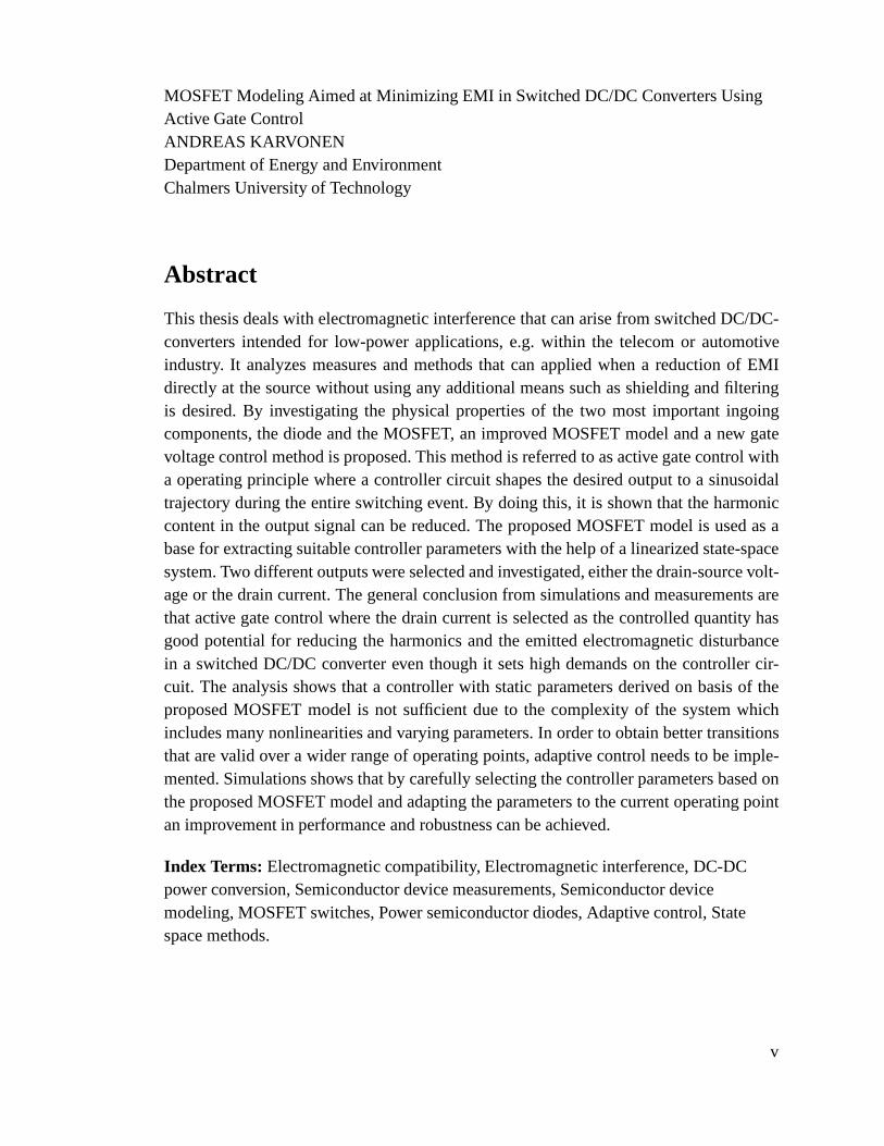
A common application for a MOSFET is when it is used in a configuration together withan inductive load and a freewheeling diode, a typical schematic of this circuit can be seenin Figure 2.12. A pulsed voltage,vG, with high current delivering capacity is applied tothe gate terminal which forces the MOSFET to turn on and off respectively.
Lload
RGVin
VG
Lσ
Fig. 2.12Test circuit to analyze switching behavior of a MOSFET.
For simpler understanding, the diode is assumed to have zeroor very small reverse re-covery time, i.e the diode does not build up any plasma or enters double injection modeduring the conducting phase. This can be a quite realistic assumption if the application isintended for lower voltage, hence a schottky diode can be applied. The turn-on character-istics can be seen in Figure 2.13.
At t = 0, a positive voltage is applied to the gate terminal. The charging of the internalgate capacitances starts and the gate voltage increase during the intervalt0 < t < t1 canbe described according to
vGS(t) = VGS(on)
(
1 − exp
(
− t
RG(CGS + CGD)
))
(2.19)
wherevG(on) is the applied voltage,RG is the gate external and internal resistance, andCGS andCGD are the lumped gate-source and gate-drain capacitances respectively.
At t = t1, the gate voltage reaches the threshold level and a drain-source current can startto flow. The drain source current is starting to build up in theMOSFET. As long as theentire current has not commutated to the diode, it will remain forward biased and carry acurrent. The commutation will not be over until the current through the MOSFET reachesthe inductor current and the diode will become reverse biased. The voltage over the MOS-FET will be equal to the sum of the DC resistance voltage and the voltage drop over thestray inductance in the MOSFET. As long as the voltage over drain source is relativelyhigh, the gate drain capacitance (CGD), which mainly consists of the depletion layer ca-pacitance, will be much smaller than the gate source capacitance (CGS). This means that
26
2.5. The MOSFET
Vth
vDS
idrain
t
t
t
IL
VG(on)
VDS(on)
Vin
vGS
VPULSE
t1 t2 t3 t4
idiode,
iload
tt0
V vPULSE, GS
iloadidiode
idrain
Fig. 2.13Turn-on diagram of a MOSFET.
27

Chapter 2. Semiconductors and Converters
the voltage over the drain source will not have a significant effect on the gate voltage.Also, the current to the gate charges bothCGD andCGS.
At t = t2, the commutation process is completed and the MOSFET is carrying the total in-ductor current which implies the start of a plateau on the gate source voltage. This plateaucomes from the conditions set by the inductor and the diode. The inductor is assumed tobe so large that the total current during the turn on process is constant and the diode isassumed to be ideal, i.e. it does not produce any reverse current peak during turn off. Thedrain current does not increase any further which gives a plateau in the gate-source volt-age. This plateau also forces the gate current to only chargethe gate drain capacitance.If this capacitance would have been constant, the derivative with which the voltage fallswould have been constant and only determined by the gate current. This is not the casesince the gate-drain capacitance increases with decreasing voltage; the derivative ofvDS
decays with time, i.e. the voltage softly drops towards its steady state value.
At t = t3, the drain source voltage has fallen to such a level that the MOSFET no longeris operating in the saturated region. In order to still support the current, the gate voltageis being increased. The drain source voltage is now at such alow voltage level that thechange in gate capacitance (CGS andCGD) will only be determined by the change in gatepotential. Hence, a small value of the total gate capacitance (CGS andCGD) will resultin a faster decrease of the drain source voltage. When the gate voltage reaches the finalvalue (VG(on)), the turn on process is completed.
2.5.5 Turn-Off Behavior of the MOSFET
With the circuit shown in 2.12, the turn-off process of the MOSFET can also be analyzed.When the MOSFET is turned on and carrying the full inductor current, a turn off processcan be started in order to commutate the current to the diode.The turn off process of apower MOSFET transistor is shown in Figure 2.14.
Beforet = 0, a positive voltage is applied to the gate terminal, the device is fully conduct-ing. At t=0, the gate voltage is suddenly decreased to 0 V. The dischargeof the internalgate capacitances starts and the gate voltage decrease during the intervalt0 < t < t1 canbe described according to
vGS(t) = VGS(on)
(
1 − exp
(
− t
RG(CGS + CGD)
))
(2.20)
whereVG(on) is the applied voltage,RG is the gate external and internal resistance, andCGS andCGD are the lumped gate-source and gate-drain capacitances respectively. Notethe obvious similarity to (2.19) that sets the increase of the gate voltage during the earlystage of the turn-on process. The time constant found in the denominator differs though,
28

2.5. The MOSFET
Vth
vGS
vDS
idrain
IL
VDS(on)
VG(on)
Vin
t
t
t
vGS
VG
t1 t2 t3 t4t0
t
idiode,
iload
iload
idiode
idrain
Fig. 2.14Turn-off of a MOSFET. The diagram shows curves of the drain current iDS , the drain-source voltagevDS and the gate source voltagevGS .
29

Chapter 2. Semiconductors and Converters
this due to the voltage dependency of the gate drain capacitance. As long as the MOSFETis turned on, the gate drain voltage is low which results in a large value ofCGD. Also, thegate drain capacitance can this time interval be assumed to be constant since the changein gate drain voltage is relatively small.
At t = t1, the MOSFET leaves the ohmic region and enters the saturatedregion. Thecommutation process between the diode and the MOSFET can notstart until the diodebecomes forward biased. Circuit analysis shows that as longas the drain source voltageis below the DC-voltage level, the diode will be reverse biased, hence no commutationcan start. If the turn off process is observed in a transfer characteristics diagram, it canbe seen that the gate voltage no longer can decrease in order for the MOSFET to carrythe total inductor current. This gives a plateau in the gate voltage. Due to this plateau, thegate current can not discharge the gate source capacitance during this phase; the entiregate current is discharging the gate drain capacitance. As the gate drain voltage continuesto increase, the gate drain capacitance also shows a sudden decrease which gives an in-creasing voltage derivative as the time approachest = t2.
At t = t2, the voltage over the MOSFET becomes equal to the DC-voltagewhich givesa possibility for the diode to start conducting. The drain source current is no longer con-strained to the full inductor current, hence can the decrease in gate source voltage con-tinue. The sudden decrease in gate voltage is reflected in thedrain current, the inductoralso sees this current drop and sets up a reverse voltage thatmakes the diode forwardbiased. If stray inductances are added, a reverse voltage isset up when the drain current isreduced. This voltage is added on top of the drain source voltage and its maximum valueoccurs when the change in drain current is at largest, i.e. right aftert = t3.
At t = t3, the commutation process is completed and the gate voltage drops below thethreshold voltage.
2.5.6 The MOSFET model in SPICE
The FET model in SPICE is based on physical properties of the FET; i.e. in an ideal case,a set of easily measurable process parameters are compiled which gives a fully functionaland adequate FET model. In practice, this is often not enoughwhich gives the demand ofadditional electrical parameters. Hence, the parameters of a FET model are often dividedin two groups; physical (e.g. gate oxide thickness) and electrical. The level 1 MOSFETmodel is the original SPICE model developed in the late 1960s. The threshold voltage isdefined as constant (VTO) which originates from an investigation of the device geometryand the ingoing materials properties such as doping levels,a full derivation can be foundin Appendix B. When the external voltage exceeds the threshold level, the drain source
30

2.5. The MOSFET
current is modeled by mobility equations. The basic equation for the drain source currentif operating in the linear region is
IDS(linear) =µWeffCox
Leff
[
(VGS − Vth)VDS − V 2DS
2
]
(1 + λVDS) (2.21)
whereWeff andLeff are the effective channel width and length, respectively.Cox is thegate oxide capacitance,µ is the carrier mobility (the SPICE parameterUO) andλ (theSPICE parameterLAMBDA) is a channel length modulation parameter. As seen, thedrain current in the linear region is based on external applied voltages such asVDS andVGS, but also on the model geometry, actually the channel length(Weff andLeff ). Thetermλ is an introduced term that represents the separation of the saturation current abovethe saturation point; indirectly it models the channel length modulation. As the MOSFETis being operated in the saturated region the drain current is described as
IDS(saturation) =µWeffCox
2Leff
(VGS − Vth)2(1 + λVDS) (2.22)
whereWeff andLeff once again are the effective channel width and length, respectively.Cox is the gate oxide capacitance,µ is the carrier mobility (the SPICE parameterUO) andλ (the SPICE parameterLAMBDA) is a channel length modulation parameter.
In SPICE are the charge storage represented by thee internalcapacitances;CGS, CGD
andCGate−Bulk . In a power MOSFET context is the gate-bulk capacitance is neglectedsince the drain is connected to the epitaxial bulk layer. Thegate-source and gate-draincapacitances are expressed as functions of applied voltages, channel width and operatingregion. The functions are not adapted for vertically diffused structures which makes theminadequate for power MOSFET simulations. Further details regarding the SPICE level 1,2 and 3 models can be found in [18, 5].
2.5.7 PSPICE MOSFET Models Adapted for Switching Applications
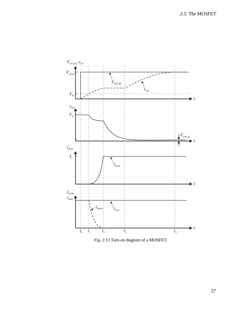
The standard SPICE MOSFET model is, as previous chapter describe, originally intendedand optimized for lateral, low power structures. The most common way to adapt the MOS-FET model to a power MOSFET structure and to solve the problemof inadequate model-ing during the switching process with Level 1 and Level 2 models is to add extra elementsthat represent the different features of a power MOSFET e.g.variable gate-drain capaci-tance and internal body diode.
A solution to the problem proposed by International Rectifier Inc. is assuming a SPICElevel 1 MOSFET model as the main component. The additional parameters added are arepresentative body diode, terminal inductances, terminal resistances and a variable ca-
31
Chapter 2. Semiconductors and Converters
pacitance in series with a variable voltage source [84]. SeeFigure 2.15 for an equivalentschematic.
Gate
Drain
Source
LG RG
LD
LS
R1E1 RDiodeCX
RS
IDiode
CGS
ID
SPICE Level 1MOSFET Model
SPICE DiodeModel
Fig. 2.15SPICE model of a HEXFET power MOSFET as proposed by International Rectifier
In Figure 2.15,LG, LD andLS represent the gate, drain and source bond wire induc-tances, respectively.RG is the internal series gate resistance,R1 is the epitaxial layerbulk resistance,RDiode is the diode bulk resistance andRS is the source lead and bondwire resistance. The diode characteristics are represented by a current sourceIDiode thatmodels the relationship between the diode voltage and the diode current. The gate-draincapacitance is modeled by a polynomial capacitorCX whose coefficients are given in thedatasheet as(VGE)n wheren is the power of the polynomial. In series with this capacitoris a polynomial voltage dependent voltage source (E1) connected. This element has nophysical reality; it is only used to modify the voltage across CX in such a way that thecombination ofCX andE1 emulates the behavior ofCGD in the real device. The high or-der of polynomial curve fitting may give rise to convergence problems which has resultedin a successive phasing out of this model type.
Many modern SPICE models provided by International Rectifier are extracted by the com-pany MODPEX. This model uses the same principle; a level 1 SPICE MOSFET model asa base with additional components that models the power MOSFET features. The maindifference is how the voltage dependent drain source capacitor is represented. The currentin a capacitor can be described as
32

2.6. EMI Generated by Switched DC/DC Converters
i(t) = Cdvc(t)
dt(2.23)
wherevc is the voltage over the capacitor andC is the capacitance. By measuring thechange in gate drain voltage and multiply it with a constant,an analogous capacitor cur-rent can be achieved. In the MODPEX model, the gate drain voltage is connected via aRCD-network which symbolizes the capacitor and the deriving function. MODPEX ex-tracts the model parameters through the use of an optimizer engine, which varies themodel parameters to minimize the error of the model performance to the digitized datasheet performance values.
Almost all semiconductor manufacturing company has some kind of model, see [85] fordescription of Siemens (now owned by Infineon) SIMPOS modelsfor switching applica-tions and [86] for SPICE models provided by Fairchild Semiconductors.
2.6 EMI Generated by Switched DC/DC Converters
2.6.1 Hard Switching Converters
By definition, a hard switching converter, eg. a step down converter, is a converter inwhich the switching element carries the whole input voltageand current as it changesstate at e.g. turn-on. In the beginning of a turn-on interval, the transistor begins to con-duct which gives that the voltage will start to fall at the same time as current begins toflow. A similar event occurs as the transistor turns off; the full current starts to fall as thevoltage over it increases. In such a converter, the simplestway of reducing EMI is byturning the device on and off during a longer time interval inorder to reducedv/dt anddi/dt. However, the simultaneous presence of voltage across the transistor and currentgives increased switching losses. The final solution of converter performance becomes atrade off between switching losses, EMI performance and component cost. To improvethe EMI performance without having to increase the switching losses, a snubber can beadded across the switching element that reducesdv/dt anddi/dt of the power device.Further reading about snubbers can be found in e.g. [19].
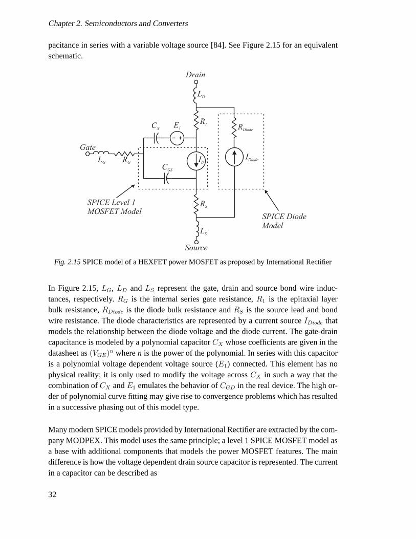
Tihanyi [20] states that for an hard switched converter witha transformer, the primarycauses of harmonics in the output are the leakage inductanceof the transformer and theheat sink applied to the switching element. If a heat sink is used, it is often grounded due tosafety reasons and must then be isolated from the the semiconductor by a dielectric washersince the terminal of the MOSFET that connects to the heat sink is usually connectedto the drain. This causes a high potential to be applied over the stray capacitor formedbetween the drain terminal and the grounded heatsink. The applied voltage gives rise to
33
Chapter 2. Semiconductors and Converters
the flow of a common mode current in the converter, see Figure 2.16.
Insulator
RG
TO220 Package
Copper Sheet
Cstray
Fig. 2.16Proper way of isolating a heat sink to minimize EMI
One way to reduce the problems caused by stray capacitance isto use the technique pro-posed in Figure 2.16 where a copper sheet is used in combination two isolating sheets.The copper sheet is connected to the source terminal of the MOSFET and acts as a Fara-day shield that reduces the stray capacitance. A variant of this is proposed by IXYS andis used in their ISOPLUSTM package that isolates the semiconducting material from theheat sink. It also effectively reduces the stray capacitance to the heat sink and allows forseveral semiconductors to be mounted on the same flange [21].Note that the previousdiscussion has only comprised of the conducted emissions, also radiated emissions needto be considered when dealing with heat sinks. According to Felic [22], a heat sink mayaffect the radiated emission of a switched DC/DC converter.The electric field amplitudespectrum at certain frequency ranges is generally enhancedby the application of a heatsink acting as an antenna which makes the antenna effect necessary to take into consider-ation in certain cases.
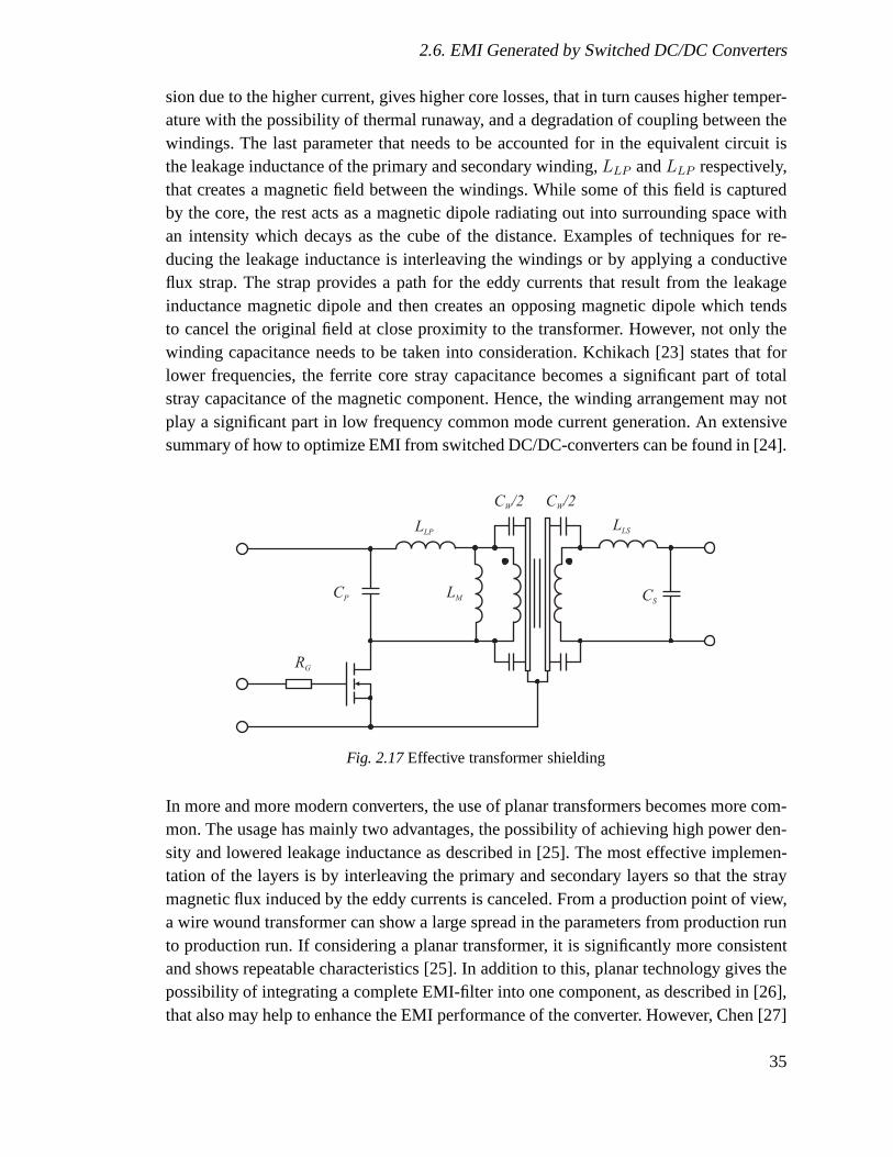
Another common cause of EMI is the stray inductance and capacitance of the transformerthat often is used in a SMPS, an equivalent circuit is shown inFigure 2.17. The equivalentcircuit models the interwinding capacitance asCW . This capacitance causes the problemof common mode emissions in isolated power supplies in a similar way as for the heatsink. One effective way of decreasing the interwinding capacitance is by applying a fara-day shield between the windings. The shield usually consists of a copper sheet connectedto the primary ground of the transformer. Note that a proper connection of the faradayshield is important; a bad connection to eg. the secondary side of the transformer canhave the the opposite effect where the conducted common modenoise measured by LISNat the feeding end is increased due to injection of secondarycommon mode noise. Theintrawinding capacitances,CP andCS are small and usually negligible at the operatingfrequencies of switching power supplies and controllers. Alarge magnetizing inductance,LM , causes a large magnetizing current which may lead to saturation of the transformercore. As for inductors, saturation of a transformer will increases the magnetic-field emis-
34
2.6. EMI Generated by Switched DC/DC Converters
sion due to the higher current, gives higher core losses, that in turn causes higher temper-ature with the possibility of thermal runaway, and a degradation of coupling between thewindings. The last parameter that needs to be accounted for in the equivalent circuit isthe leakage inductance of the primary and secondary winding, LLP andLLP respectively,that creates a magnetic field between the windings. While some of this field is capturedby the core, the rest acts as a magnetic dipole radiating out into surrounding space withan intensity which decays as the cube of the distance. Examples of techniques for re-ducing the leakage inductance is interleaving the windingsor by applying a conductiveflux strap. The strap provides a path for the eddy currents that result from the leakageinductance magnetic dipole and then creates an opposing magnetic dipole which tendsto cancel the original field at close proximity to the transformer. However, not only thewinding capacitance needs to be taken into consideration. Kchikach [23] states that forlower frequencies, the ferrite core stray capacitance becomes a significant part of totalstray capacitance of the magnetic component. Hence, the winding arrangement may notplay a significant part in low frequency common mode current generation. An extensivesummary of how to optimize EMI from switched DC/DC-converters can be found in [24].
CP
RG
LM CS
LLPLLS
C /2WC /2W
Fig. 2.17Effective transformer shielding
In more and more modern converters, the use of planar transformers becomes more com-mon. The usage has mainly two advantages, the possibility ofachieving high power den-sity and lowered leakage inductance as described in [25]. The most effective implemen-tation of the layers is by interleaving the primary and secondary layers so that the straymagnetic flux induced by the eddy currents is canceled. From aproduction point of view,a wire wound transformer can show a large spread in the parameters from production runto production run. If considering a planar transformer, it is significantly more consistentand shows repeatable characteristics [25]. In addition to this, planar technology gives thepossibility of integrating a complete EMI-filter into one component, as described in [26],that also may help to enhance the EMI performance of the converter. However, Chen [27]
35

Chapter 2. Semiconductors and Converters
states that a planar transformer has the disadvantage of increased intrawinding parasiticcapacitances,CP andCS, and increased interwinding capacitance,CS. The increase ofthese capacitances gives rise to higher differential mode and common mode noise magni-tude, respectively, as shown in [27].
2.6.2 Simulating EMI from a Switched DC/DC Converter
When it comes to predicting the overall performance of a switched DC/DC converter,several factors complicate the results and the accuracy of the simulation. At first, themost common language for simulating electronic components, SPICE, is not originallyintended as a simulator for switched elements. As describedin Section 2.4.4 and 2.5.7 re-spectively, the performance of included models for MOSFETsand PiN-diodes can showsignificant discrepancies with real component behavior. This becomes a problem worthconsidering when designing switched DC/DC converters since these two components areextensively used. The second factor that contributes to difficulties in simulation is thelarge amount of parameters that affect the results and the difficulties to determine them.Kyriazis [28] uses a basic approach with a model over the converter that considers boththe parasitic capacitance in the transformer and from the heat sink. Once these parametersare known, equivalent circuits over both common and differential mode conducted emis-sions can be performed. However, the model shows significantdiscrepancies in simulationresults and measurements for higher frequencies (1Mhz) andthe versatility is drasticallyreduced due to difficulties in determining the parasitic capacitances in the circuit.
A more general approach for simulating EMI is proposed by Jinin [29, 30] where a EMIprediction tool based on approximating the switching eventhas been implemented. Thetool focuses on finding the correct current and voltage derivatives,di/dt anddv/dt, dur-ing the switching event by studying an behavioral model of the IGBT and approximate theswitching transients with a piecewise linear function. By doing so, the practical switchingcharacteristic can be reconstructed in the EMI noise quantification study. A comparisonshowed that this method improved the simulated EMI spectrumcompared with trape-zoidal switching events. This method vouches for a simple method to evaluate the EMInoise, however, the major deficit is it only can be quantified once the switching event isknown in detail.
Other methods of determining the EMI performance of switch mode converters have beenproposed in eg. [31] where a state variable approach is used together with stray param-eter extraction from a PEEC-program. Also, complete programs have been developed tocalculate EMI-levels [32]. These programs are often based on several simplifications thatmakes their versatility limited.
36

2.6. EMI Generated by Switched DC/DC Converters
When radiated disturbances are to be modeled, much more complex simulation modelsare needed, often in full 3D. In a paper by Ala et. al [33] a full3D numerical model basedon the finite difference time-domain (FDTD) method is proposed. The method allows thestudy of geometrically complicated structures which are supposed to simulate a realisticelectromagnetic environment in eg. a hybrid vehicle. The most advantageous benefit withthe proposed method is that only a current measurement in thetime domain is needed topredict the radiated emissions. However, the complexity ofthe FDTD-model makes it dis-advantageous since it requires a good knowledge of the environment where the converteris to be placed.
2.6.3 Random Switching
Several studies have been performed in the past that shows reduced levels of EMI fromswitched DC/DC converters that are using some kind of non-deterministic property ap-plied to the switching pattern. The key property that differentiates random switching ina switch mode power converter from regular switching, whichgenerates time-periodicswitching functions, is that random switching produces switching functions that have anon-deterministic, random component. If a random switching converter is well designed,it can behave similarly to a regular converter, i.e., generating a switching function thatallows the reference signal to be extracted by a low-pass filtering and transferred to theload. As a consequence of the non-repetitive switching functions, the frequency-domainspectra for randomized modulators are different from the spectra caused by a determin-istic modulation strategy. For classic PWM modulation, thespectrum mainly consists ofdiscrete frequency components clustered around multiplesof the PWM carrier frequency,whereas a random modulator transfers the power carried by the harmonics into a con-tinuous density spectrum. The main purpose with this chapter is to present a study overthe present work performed on random switching converters.However, no own work isperformed on this subject, it is only attached to illustratean alternative method to reduceEMI from a switched DC/DC converter.
Although a randomized switching pattern can be applied as shown in eg. [34, 35, 36, 37]where field oriented control and speed vector-control of induction machines are investi-gated, the main field of interest in this thesis lies on how random switching can be appliedto DC/DC converters. Hence is no further attention spent on DC/AC applications butrather on basic random switching principles and their application to DC/DC-converters.A thorough review of the current research is presented in [38] which is followed to a largeextent in this report.
A randomized modulation scheme is characterized by an invariant deterministic and prob-
37

Chapter 2. Semiconductors and Converters
abilistic structure. If considering the reference switch pattern, dither is added that does notchange from one switching cycle to the next. At each new cycle, the same probabilisticstructure is used which means that there are no variations inthe requirements on averagequantities such as the duty ratio. Based on this, the stationary switching schemes can befurther classified into three main categories:
• Randomized Pulse Position Modulation (RPPM)
• Randomized Pulse Width Modulation (RPWM)
• Asynchronous Switching Schemes, both simplified and regular
Figure 2.18 shows a switching function that consists of several consecutive random switch-ing cycles.ξk is the time at which the the cycle starts,Tk is the duration of thek:th cycle,ak is the duration of the on-state within this cycle, andεkis the delay to the turn-on withinthe cycle. Note that the duty ratio isdk = ak/Tk. All of the above mentioned switchingschemes can be achieved by altering some of the parameters shown in Figure 2.18. Ingeneral, one can ditherεk, ak or Tk individually or simultaneously.
q(t)
u (t- )k kξTkξk ξk+1
εk
ak
Tkξk ξk+1
εk
ak
t
t
Fig. 2.18The switching waveformq(t) and the pulseu(t − ξk) representing just thek:th cycle ofq(t).
If randomized PPM is studied, each cycle has the same lengthTk, and the pulse in each cy-cle has the same durationak , but an independent random variation in the positionεk of thepulse in thek:th cycle is allowed. Randomized PWM triggers the pulse in the beginningof each period, i.e.εk = 0, and varies the duration of the pulseak. The total switching pe-riod Tk remains fixed. Not that in contrast to conventional switching that for eg.ak = 0.5
has only odd harmonics, randomized PWM yields discrete harmonics at even multiplesof the switching frequency as well. According to Stankovic[39] both RPPM and RPWMare efficient ways of reducing the size of discrete harmonicsand in satisfying narrow-band constraints. However, due to its widespread nature, random switching techniques
38

2.6. EMI Generated by Switched DC/DC Converters
are much less effective in dealing with wide-band requirements. If the two previouslymentioned techniques are compared, randomized PWM can reduce the fundamental fre-quency component in the power spectra more than randomized PPM. On the other handis randomized PPM more efficient at reducing higher discreteharmonics.
A true asynchronous modulation technique, proposed by Tanaka [40], adds a random vari-ation to the period time of the pulse,Tk. The time delay at the beginning of each pulse,εk = 0, is set to zero and the pulse width,ak, is also kept constant. The true asynchronouscan also be simplified as proposed by Tanaka in [41]. This is done by varying the periodtime of the pulse,Tk, but keep the on-state at a constant length, i.e.ak. Both of thesemethods are proven to give lower power density spectrum [40,41].
One of the main motivations for use of randomized modulationis the possibility of acous-tic noise reduction in inverter-based motor drives. A motordrive benefits from the ran-domized switching strategy by a better utilization of the available harmonic content ofwaveforms at the interface where the power supply connects to the motor. However, in eg.modern telecommunication systems, sensitive consumers such as radio applications canbe interfered by high spectral power density concentrated to a certain frequency, this canbe seen as a spuriose on the carrier frequency. Random switching schemes can for thatreason offer a fairly wide range of waveform spectra to choose from. The added degreesof freedom allows for a more effective optimization of signal power at specific frequen-cies and frequency bands of interest. When compared with deterministic waveforms andswitching schemes, the main effect of randomization is a reduction of the discrete spec-trum and consequently also an introduction of a continuous spectrum. Depending on whattype of equipment that is connected to the power supply, the consequences of randomizedintroduction can vary. For instance, the damaging effect ofharmonic torque pulsationsin electric motors is more severe than that of wideband fluctuations of the same overallpower. In general, the impact of randomization is likely to be positive for systems thatare susceptible to narrow-band interference, like digitalcircuits, rotating machinery andcommunication systems. while many types of communication systems are sensitive tonarrow-band interference, the actual performance is very much dependent on the partic-ular communication method. Hence can randomized modulation can be seen as a part ofemerging digital energy systems that aim to achieve efficiency while minimizing undesir-able effects on the environment like EMI, vibrations and acoustic noise.
Shrivastva [42] states that a new method referred to as a discrete RPWM scheme can beof interest of reducing EMI problems since virtually no harmonics of the switching fre-quency are present in the output power spectrum.
Note that not only random parameter modulation such as RPWM and RPPM can be of
39

Chapter 2. Semiconductors and Converters
interest. Another technique proposed by [43, 44, 45, 46] that can be of interest is wherethe switching frequency is modulated by a much lower modulation frequency. All authors[43, 44, 45, 46] unanimously agrees that that by modulating the switching frequency, areduction in the peak levels of conducted electromagnetic disturbances (both commonand differential mode) can be achieved. The switching frequency,fc, is modulated witha frequency,fm, with an amplitude of frequency change∆f , that helps to spread out thespectrum. The principle of how the spectra is spread is shownin Figure 2.19.
fc nfc
1/fc
fc nfc
]/)2sin(1[
1
cmc ftfff ???
fm
fm
Fig. 2.19Comparison of spectra from a square waveform and a frequencymodulated square wave-form.
The modulation frequency is typically selected much lower than the switching frequency.Feng and Cheng [45] suggests a modulation frequency,fc, of 200Hz for a converter thatoperates with 150kHz switching frequency. Note that the total power of the signal is un-affected by frequency modulation. The total power of a signal equals to the summationof the square of each harmonic amplitude. The general tendency of frequency modulationis to spread out the power of each switching harmonic. The higher the harmonic number,the more even is the spread-out power [45]. However, Gonzalez [43] states that due tothe fluctuations in the output voltage, the technique of carrier modulation is better suitedfor DC/AC applications that can tolerate these small fluctuations better than a DC/DCconverter with high output tolerances. Another deficit stated in [44] that needs to be takeninto consideration is the interaction of the modulation frequency within the control-loopthat might lead to a deteriorated EMI-performance.
2.6.4 Gate Voltage Control
Traditionally, the EMI from a hard switched converter have been controlled by reducingdv/dt of the switching element in the circuit as described by e.g. Clayton [47]. By doingthis, the spectral content in the switching waveforms will be decreased. However, doing
40
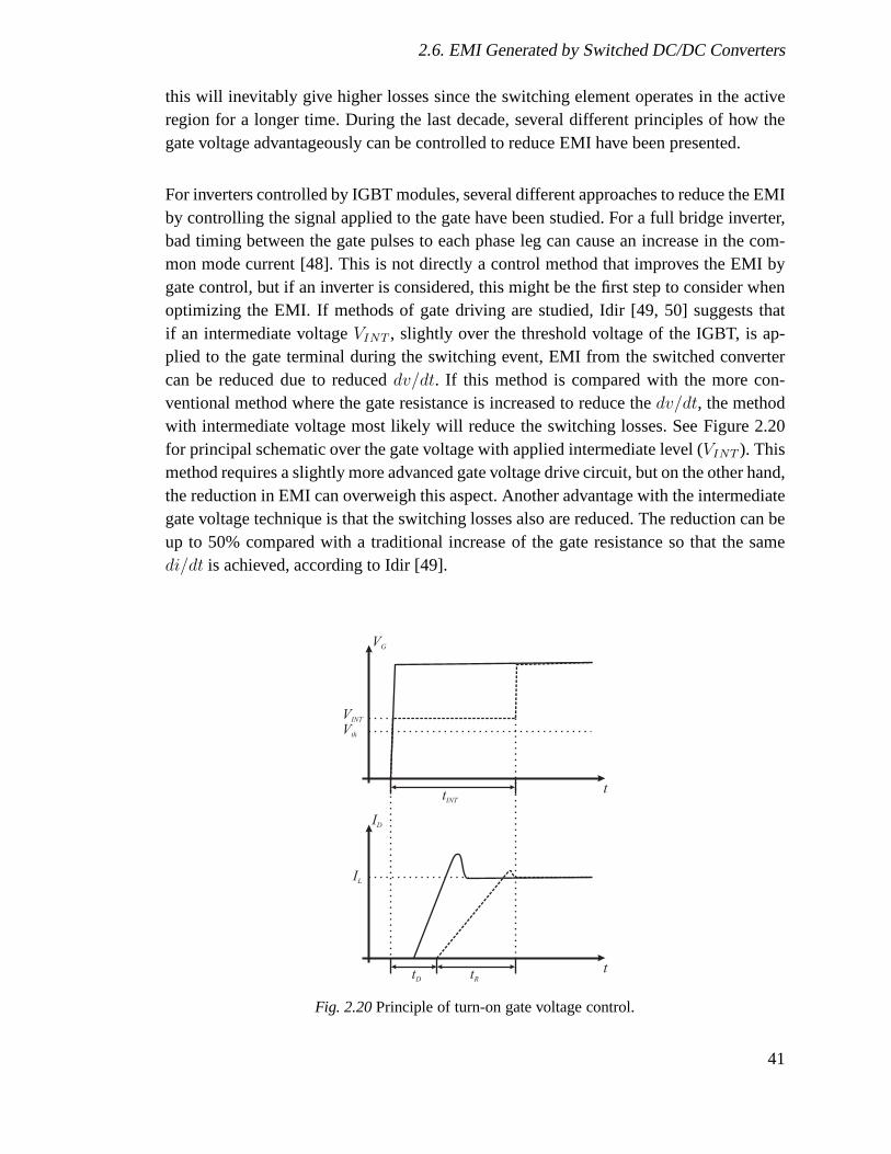
2.6. EMI Generated by Switched DC/DC Converters
this will inevitably give higher losses since the switchingelement operates in the activeregion for a longer time. During the last decade, several different principles of how thegate voltage advantageously can be controlled to reduce EMIhave been presented.
For inverters controlled by IGBT modules, several different approaches to reduce the EMIby controlling the signal applied to the gate have been studied. For a full bridge inverter,bad timing between the gate pulses to each phase leg can causean increase in the com-mon mode current [48]. This is not directly a control method that improves the EMI bygate control, but if an inverter is considered, this might bethe first step to consider whenoptimizing the EMI. If methods of gate driving are studied, Idir [49, 50] suggests thatif an intermediate voltageVINT , slightly over the threshold voltage of the IGBT, is ap-plied to the gate terminal during the switching event, EMI from the switched convertercan be reduced due to reduceddv/dt. If this method is compared with the more con-ventional method where the gate resistance is increased to reduce thedv/dt, the methodwith intermediate voltage most likely will reduce the switching losses. See Figure 2.20for principal schematic over the gate voltage with applied intermediate level (VINT ). Thismethod requires a slightly more advanced gate voltage drivecircuit, but on the other hand,the reduction in EMI can overweigh this aspect. Another advantage with the intermediategate voltage technique is that the switching losses also arereduced. The reduction can beup to 50% compared with a traditional increase of the gate resistance so that the samedi/dt is achieved, according to Idir [49].
t
ID
VG
ttINT
tD tR
VINT
IL
Vth
Fig. 2.20Principle of turn-on gate voltage control.
41

Chapter 2. Semiconductors and Converters
Tazikawa [51] proposes a method where different sizes of gate resistors are connected dur-ing different phases of the turn-on and turn-off process respectively. This method reducesthedi/dt in the current flowing through the converter, avoids collector voltage overshootsand reduces the EMI. The disadvantages is that the method is based on the existence of astray inductor and that the control becomes significantly more complicated.
Another control method is when the gate signal is divided into two stages as proposed ineg. [52, 53]. In the two-stage method, thedi/dt of the transistor current is controlled asusual, but in the Miller-phase during turn-on, an additional current generator is connectedto the gate that adds extra energy to the gate and shortens thetime in which the transistoris operating in the active region, i.e. increasing thedv/dt. Hence will a lowered EMI benoticeable, but also lower switching losses due to the shorter time in the active region.Musumeci [54] has developed this technique by implementinga phase locked loop thatdetects the transition into the Miller region. Another development of the two-stage switch-ing strategy is proposed by Kagerbauer [55] where the possibility to dynamically adjustthedv/dt on a pulse-by pulse basis is introduced. The main feature of the control circuitis an external capacitor,Cm, that is connected from the gate to the collector. The capac-itor acts as an external Miller capacitance connected in parallel with the internal Millercapacitance of the MOS switching element. During the turn-on or turn-off event, both theinternal and external Miller capacitors are charged or discharged by the gate current. Thecurrent through the external Miller capacitor is routed through an electronically controlledcurrent mirror circuit that injects a current into the gate.This current is proportional to theexternal Miller capacitor current and contributes to a change in the voltage transition rate.
Kempski [56] states that thedv/dt of the voltage over the switching element can be chosenin such a way that the oscillations in the circuit are canceled due to resonances in thecircuit. A slight change in rise time can change the resonantbehavior so that the commonmode current is minimized.
42

Chapter 3
Semiconductor Modeling
In order to simplify the construction process of applications that includes semiconductors,it is of great importance that the construction can be simulated, both when regardinga single component and as a complete system. However, when dealing with switchedDC/DC applications, some of the models show deficits that maydecrease the accuracy.When dealing with PiN-diodes, models for more accurate switching characteristics havebeen proposed in several articles; models intended for power applications and SMPS havebeen investigated in e.g. [13, 12, 57]. In the following sections a novel PiN-diode modelbased on charge node locations is investigated. Also, an overview of MOSFET modelingincluding the introduction of a new novel model based on circuit analysis is presented.
3.1 Nodal Analysis Vs. State Variable Approach
In classical nodal analysis, a consistent set of simultaneous equations is obtained by in-voking Kirchhoff’s current law for each node in the circuit.The currents are expressed interms of all the branch currents leaving a node equated to theforcing currents entering thenode. The currents and voltages can in matrix notation be written as
G ∗ v = i (3.1)
whereG is the conductance matrix,v is the voltages in each node andi is the currentsources in the circuit. The most significant drawback of classical nodal analysis (imple-mented in e.g. the first versions of SPICE) is that independent voltage sources, transform-ers and dependent sources do not enter into nodal analysis ina natural way and have to betransformed using a variety of algorithms to get the equations into suitable form. In orderto avoid this problem, Modified Nodal Analysis (MNA) can be incorporated as proposedby eg. [58, 59]. Modified nodal analysis removes most of the limitations of the classicalnodal method and is according to [59] suitable for symbolic and numeric analysis of elec-trical circuits. MNA is applied later versions of SPICE which solved the problem with
43

Chapter 3. Semiconductor Modeling
independent voltage sources.
Practical circuits contain many nonlinear elements such asdiodes and transistors. Thecommon approach to solve these elements, e.g. diode characteristics, is by linearizationusing the Newton-Raphson method. This method is known to be very fast, but also tohave convergence problems sometimes. Semiconductor junctions (exponential relation-ships) may lead to huge currents that exceed the computers computational range.
Modified nodal analysis suffers from some drawbacks such as zero diagonal elementscaused by floating voltage sources and singularity in the subset of circuit equations forinitial state and steady-state analysis. Hence is another method named Unified NodalAnalysis (UNA) proposed by Fung-Yuel Chang in [60, 61]. The UNA formulation ofcircuit equations eliminates the singularity in Modified Nodal Analysis when deriving theinitial-state and steady-state responses without performing any transient analysis. Also,UNA works well for nonlinear circuits as well which can be considered a major advan-tage [60, 61].
However, the focus in this thesis is not aimed at speed of the solver or simple implemen-tation of the circuits in an graphical user interface but rather at investigating the stabilityof the system by using transfer functions and developing suitable controller structures.These properties makes state space representation more suitable rather than nodal analy-sis and consequently analyzed further in this thesis. The general state-space equations canbe expressed as
x(t) = f(x(t), u(t))
y(t) = g(x(t), u(t))(3.2)
wherex(t) is the states,u(t) is the input to the system andy(t) is the output of the system.If (3.2) is applied to a linear system, it can be rewritten as
x(t) = Ax(t) + Bu(t)
y(t) = Cx(t) + Du(t)(3.3)
whereA, B, C andD are matrixes. The state space representation provides a convenientand compact way to model and analyze systems with multiple inputs and outputs. Theuse of the state space representation is not limited to systems with linear components andzero initial conditions which makes it suitable for the analysis performed in this thesis.The perhaps most important feature of the state space representation is that the stabilityand response characteristics of a system can be studied fromthe eigenvalues of matrixA.
44

3.2. Improving and verifying the diode model
3.2 Improving and verifying the diode model
When a diode is modeled, there are mainly two different properties that needs to be con-sidered, namely how the junction capacitance is modeled andthe behavior of the reverserecovery current. Hence are these two aspects investigatedfurther and the results are pre-sented below. The main objective with this investigation isto verify the capacitance of apn-junction which is a part of a power MOSFET, see Section 3.3.3 for applications.
3.2.1 Determining the pn-Junction Capacitance
As previously mentioned, the traditional SPICE model of a diode describes the junc-tion capacitance as explained in Section 2.2.1. This capacitance is of great importance inswitched DC/DC converters since the interaction of this capacitance and other parasiticcircuit elements can cause oscillations and other unwantedbehavior in the circuit. Ac-cording to Lucia [62], the total junction capacitance showsa frequency dependence thatbecomes apparent when the diode is forward biased. This dependence originates fromthe diffusion capacitance that dominates the total junction capacitance when the diodeis forward biased; for low frequencies, the minority carriers that constitute the physicalmeaning of the capacitor, will follow the applied ac-signal. However, if the diode is usedas a part of MOSFET modeling which is the main application in this investigation, theimportance of the diffusion capacitance becomes comparably small since the body diodewill be operated in reverse bias for most normal conditions;small signal variations inthe diffusion capacitance is neglected for all upcoming simulations. When the diode isreverse biased, the capacitance can be considered independent of the measurement fre-quency [63, 62]. This is also shown by own measurements wherethe diode is kept reversebiased and the test frequency is varied, see Figure 3.1. Hence is the test frequency isselected to 1MHz in accordance with the de facto standard given in most data sheets.
104
105
106
107
10−11
10−10
10−9
10−8
10⋅C
1N4007
C32CTQ030
Vreverse
Vreverse
Frequency [Hz]
Cap
acita
nce
[C]
Fig. 3.1Junction capacitance as a function of the applied frequency.
The method for determining device capacitances proposed inthis thesis is based on a
45

Chapter 3. Semiconductor Modeling
constant current charger described in [64]. The test circuit is presented in Figure 3.2
LM334
CprobeDUT
Fig. 3.2Circuit diagram for a constant current charger.
The principle of the test is to charge the DUT with a constant current and measure the volt-age over the DUT. Due to the constant current, the total capacitance of the measurementobject is
Ctot =itot
dvDUT /dt(3.4)
whereCDUT is the total device capacitance andvDUT is the measured voltage. Since thedevice that is analyzed can have a capacitance with the same magnitude as the inherentprobe capacitance, this factor also needs to be taken into account. The voltage over theprobe is measured and together with the known value of the inherent capacitor (usuallyspecified by probe manufacturer), the current into the probecan be easily calculated. Dueto current sharing, the capacitance of the DUT can then easily be calculated since bothcapacitors are connected in parallel and will have the same voltage applied over them.The circuit was verified using a varactor (ZC836) due to its well defined capacitance, theresults are shown in Figure 3.3
0 0.5 1 1.5 2 2.5−15
−10
−5
0
5
v
DUT, measured
vDUT, spice
100
101
102
101
102
C
measured
CSpice
Cdatasheet
Time [µs]
Volta
ge[V
]
Frequency [Hz]
Cap
acita
nce
[F]
Fig. 3.3Analysis of the junction capacitance in the ZC836 varactor.
46
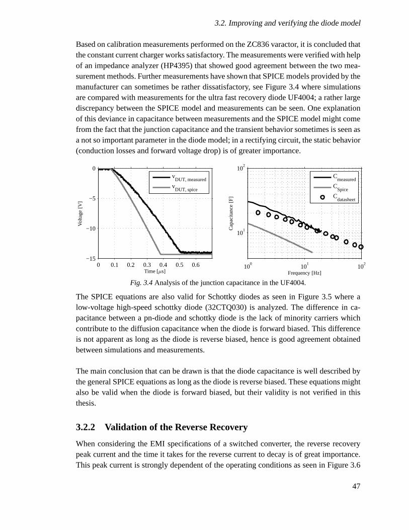
3.2. Improving and verifying the diode model
Based on calibration measurements performed on the ZC836 varactor, it is concluded thatthe constant current charger works satisfactory. The measurements were verified with helpof an impedance analyzer (HP4395) that showed good agreement between the two mea-surement methods. Further measurements have shown that SPICE models provided by themanufacturer can sometimes be rather dissatisfactory, seeFigure 3.4 where simulationsare compared with measurements for the ultra fast recovery diode UF4004; a rather largediscrepancy between the SPICE model and measurements can beseen. One explanationof this deviance in capacitance between measurements and the SPICE model might comefrom the fact that the junction capacitance and the transient behavior sometimes is seen asa not so important parameter in the diode model; in a rectifying circuit, the static behavior(conduction losses and forward voltage drop) is of greater importance.
0 0.1 0.2 0.3 0.4 0.5 0.6−15
−10
−5
0
v
DUT, measured
vDUT, spice
100
101
102
101
102
C
measured
CSpice
Cdatasheet
Time [µs]
Volta
ge[V
]
Frequency [Hz]
Cap
acita
nce
[F]
Fig. 3.4Analysis of the junction capacitance in the UF4004.
The SPICE equations are also valid for Schottky diodes as seen in Figure 3.5 where alow-voltage high-speed schottky diode (32CTQ030) is analyzed. The difference in ca-pacitance between a pn-diode and schottky diode is the lack of minority carriers whichcontribute to the diffusion capacitance when the diode is forward biased. This differenceis not apparent as long as the diode is reverse biased, hence is good agreement obtainedbetween simulations and measurements.
The main conclusion that can be drawn is that the diode capacitance is well described bythe general SPICE equations as long as the diode is reverse biased. These equations mightalso be valid when the diode is forward biased, but their validity is not verified in thisthesis.
3.2.2 Validation of the Reverse Recovery
When considering the EMI specifications of a switched converter, the reverse recoverypeak current and the time it takes for the reverse current to decay is of great importance.This peak current is strongly dependent of the operating conditions as seen in Figure 3.6
47

Chapter 3. Semiconductor Modeling
0 5 10 15 20 25 3010
2
103
104
C
measured
CSpice
Cdatasheet
Voltage [V]
Cap
acita
nce
[F]
Fig. 3.5Analysis of the junction capacitance in the 32CTQ030.
where the reverse recovery characteristics of a standard recovery rectifier diode (20ETS12from International Rectifier) is investigated by using the test circuit depicted in Figure2.12. In this circuit, the MOSFET is seen as an ideal switch since it is turned on muchfaster than the diode that is subject to test. As seen, the current peak that occurs duringreverse recovery is not only dependent on the forward current carried by the diode beforeforced to blocking state (see Figure 3.6, left picture), butvariations in the reverse voltageapplied over the diode also gives an indirect effect (see Figure 3.6, right picture).
−0.05 0 0.05 0.1 0.15 0.2 0.25−400
−300
−200
−100
0
idiode
vdiode
−0.1 0 0.1 0.2 0.3 0.4
−200
−150
−100
−50
0
idiode
vdiode
iforward
Time [µs]Time [µs]
Volta
ge[V
]/C
urre
nt[A
]
Volta
ge[V
]/C
urre
nt[A
]
Fig. 3.6Reverse recovery current as a function of the operating conditions. Left: Constant current,varying reverse voltage (Iforward = 0.5A,Vreverse = 100V, 200V, 300V ). Right: Con-stant voltage, varying forward current (Iforward = 0.4A, 1.0A, 1.8A,Vreverse = 100V ).
The reverse current peak depends on two criteria; the forward current and thedi/dt car-ried by the diode [3]. A high forward current gives a high plasma concentration in theintrinsic region which in turn results in a high reverse current peak. This is seen in Figure3.6, left picture, where the forward current is varied from0.4A to 1.8A. Theoretically isthe peak reverse recovery current linearly dependent on theforward current but for highforward currents, the peak reverse current can be saturateddue to emitter injection. Theother factor that determines the reverse recovery current is the current derivative,di/dt.
48
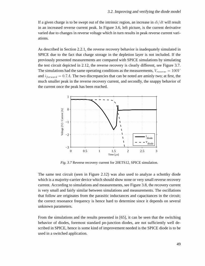
3.2. Improving and verifying the diode model
If a given charge is to be swept out of the intrinsic region, anincrease indi/dt will resultin an increased reverse current peak. In Figure 3.6, left picture, is the current derivativevaried due to changes in reverse voltage which in turn results in peak reverse current vari-ations.
As described in Section 2.2.1, the reverse recovery behavior is inadequately simulated inSPICE due to the fact that charge storage in the depletion layer is not included. If thepreviously presented measurements are compared with SPICEsimulations by simulatingthe test circuit depicted in 2.12, the reverse recovery is clearly different, see Figure 3.7.The simulations had the same operating conditions as the measurements,Vreverse = 100V
andiforward = 0.7A. The two discrepancies that can be noted are aminly two; at first, themuch smaller peak in the reverse recovery current, and secondly, the snappy behavior ofthe current once the peak has been reached.
0 0.5 1 1.5 2 2.5 3−3
−2
−1
0
1
idiode
vdiode
Time [µs]
Volta
ge[V
]/C
urre
nt[A
]
Fig. 3.7Reverse recovery current for 20ETS12, SPICE simulation.
The same test circuit (seen in Figure 2.12) was also used to analyze a schottky diodewhich is a majority-carrier device which should show none orvery small reverse recoverycurrent. According to simulations and measurements, see Figure 3.8, the recovery currentis very small and fairly similar between simulations and measurements. The oscillationsthat follow are originates from the parasitic inductances and capacitances in the circuit;the correct resonance frequency is hence hard to determine since it depends on severalunknown parameters.
From the simulations and the results presented in [65], it can be seen that the switchingbehavior of diodes, foremost standard pn-junction diodes,are not sufficiently well de-scribed in SPICE, hence is some kind of improvement needed isthe SPICE diode is to beused in a switched application.
49

Chapter 3. Semiconductor Modeling
−0.1 0 0.1 0.2 0.3−40
−30
−20
−10
0
vdiode, meas
idiode, meas
−0.1 0 0.1 0.2 0.3−40
−30
−20
−10
0
vdiode, Spice
idiode, Spice
Time [µs]Time [µs]
Volta
ge[V
]/C
urre
nt[A
]
Volta
ge[V
]/C
urre
nt[A
]
Fig. 3.8Reverse recovery current and voltage for 30CTQ030, comparison of SPICE simulationand measurements.
3.2.3 Implementation of a Diode Model Based on Charge Locations
As described in Section 2.4.4, a simple pn-diode model can beimplemented by usingthe principle of charge storage using the lumped charge model as proposed by Linvill[10]. The diode models used in circuit simulators such as SPICE are based on the originalcharge control model as described in [5]. This model includes effects of charge storageduring reverse recovery but it does not consider the effect reverse recovery effect of thediode. This gives a diode model that exhibit an instantaneous recovery during commu-tation to the non-conducting state. A more gradual or softerrecovery can be obtainedby adding extra parallel capacitance to the diode model. However, a capacitive current isnon-dissipative, associated with energy storage in the capacitor which is not the case in areal diode. The actual diode reverse recovery current is dissipative and hereby one of themost important sources of power dissipation for diodes usedin switching converters.
The original charge control diode model used in e.g. SPICE employs one charge storagenode at the boundary between the different doping regions. When the charge stored inthat node becomes exhausted during reverse conduction, thediode instantly switches toreverse blocking mode. This is not the case in an actual PiN-diode where reverse recov-ery is caused by diffusion of charge from the center of the intrinsic region. One way toimprove the behavior is to utilize a diode model proposed by Lauritzen [14] that utilizesfour charge storage nodes. The total model is described by (2.15) to (2.17) that describesthe diffusion current through the intrinsic region. If thisdiode model is implemented inMatlab/Simulink and suitable parameters are extracted according to the procedure in [14],a diode model with reverse recovery may be obtained. For illustrative purposes, the diodemodel for ETS12 is implemented together with a switching element consisting of a MOS-FET to form the circuit depicted in 2.12. The simulation results are presented in Figure
50

3.3. A Novel MOSFET Model Based on Circuit Analysis
3.9 are obtained. Note that the MOSFET model used in all simulations presented aboveis the empirical model provided by the manufacturer International Rectifier.
0 0.01 0.02 0.03 0.04 0.05−100
−80
−60
−40
−20
0
20
idiode
vdiode
Time [µs]
Volta
ge[V
]/C
urre
nt[A
]
Fig. 3.9Reverse recovery current and voltage for 20ETS12, lumped charge model.
The operating conditions in Figure 3.9 are similar to those in Figures 3.6 and 3.7, namelyVreverse = 100V andiforward = 0.7A. As seen, the reverse recovery current may obtaina more correct appearance as the intrinsic layer in the diodegets depleted as the con-ductivity decreases; the recovery current is less snappy than the current simulated by theSPICE model. However, the derivatives of the current slopesare still much higher thanthose achieved during measurements.
This method may improve the reverse recovery current but dueto difficulties in the param-eter extraction procedure, the lumped charge model proposed by Lauritzen is not inves-tigated further for the benefit of the regular SPICE model provided by the manufacturer.When MOSFET modeling is considered, as seen in the followingsection, the recoverycharacteristics are only of interest when the MOSFET is reverse biased; hence can theneed for correct recovery characteristics be considered asa minor detail in the MOSFETmodel.
3.3 A Novel MOSFET Model Based on Circuit Analysis
Many studies have been performed in how the switching behavior of a power MOSFETcan be modeled with various approaches. The usage of these models tend to be somewhatlimited and most important of all, the practical applications have been limited due to e.g.complex parameter extraction procedures. The model proposed in this thesis aims at rep-resenting the MOSFET with some relatively simple circuit elements in combination with
51

Chapter 3. Semiconductor Modeling
already known equations.
The proposed MOSFET model is depicted in Figure 3.10. The main elements are the cur-rent generator,IDS, determining the drain-source current, and the capacitorsCGS, CGD,CDS that emulates the charge accumulations in the semiconductor. Note that these ca-pacitors have no physical presence in the MOSFET; their intention is only to simulatethe charge accumulation in the MOSFET. All external connectors have a resistance,RS,RD andRS, that simulates the built in ohmic losses in each terminal. In addition to theresistance in each terminal, a parasitic series inductance, LG, LD andLS is introduced.The inductance in the bonding wires that attaches the silicon substrate with the package isnot neglectable at fast transitions such as a switching event; hence the need for a parasiticinductance.
RG
RD
RdiodeCGD
CGS Cdiode
RS
IDS
LD
LG
LS
Idiode
Fig. 3.10Circuit diagram for the proposed MOSFET model
The drain-source current (IDS) is determined as a function of the applied gate-sourcevoltage (VGS) and the drain-source voltage (VDS) by equations that are taken directlyfrom SPICE [5]. WhenVGS exceedsVth and the MOSFET is operating in the linear/ohmicregion ((VGS − Vth >= VDS)), the drain source current can be described as
IDS(linear) =µWeffCox
Leff
[
(VGS − Vth)VDS − V 2DS
2
]
(1 + λVDS) (3.5)
where several constants (µ, Weff , Cox, Leff ) scale the current to a suitable level. TheSPICE constant (λ) that models the channel length of the MOSFET is also introduced.Usuallyλ has a very low value and causes only a small slope on the outputcharacteristics,mostly in the active region. In the active/saturated region((VGS −Vth < VDS)), the drain-source current can be described as
IDS(saturation) =µWeffCox
2Leff
(VGS − Vth)2(1 + λVDS) (3.6)
where the channel length modulation parameter (λ) once again is present. As describedin Section 2.5, a feature of the VDMOS is the internal body-diode. This diode is modeled
52

3.3. A Novel MOSFET Model Based on Circuit Analysis
by a current source (Idiode), an internal series resistor (Rdiode), and a junction capacitor(Cdiode) whose capacitance shows a strong voltage dependence. Thismodel can be com-pared with the SPICE model for regular pn-junction diodes [5] and can also be found inSPICE models for power MOSFET’s provided by manufacturers,see Chapter 2.5.7.
In order to implement Figure 3.10 in Matlab/Simulink, nodalanalysis in combinationwith voltage loop analysis is used. The circuit contain six energy storing elements whosevoltage or current are selected to form the state matrix
x(t) =
vCGS
vCGD
vCdiode
iGiDiS
(3.7)
where the current through an inductor or the the voltage overa capacitor will constitutea state. For a functional circuit, the MOSFET model is implemented in a circuit togetherwith appropriate external elements. The inputs (u(t)) and the outputs (y(t)) to the systemare selected in an appropriate way to form a state-space model of the total system, see(3.3).
3.3.1 Parameter Extraction for a Power MOSFET
To be able to simulate the performance of the component, parameter extraction needs tobe performed. The procedure suggested in this thesis is based on three different sourcesof information; datasheets provided by the manufacturer, SPICE models provided by themanufacturer and component measurements. The main idea is to keep the procedure assimple as possible and use known sources of data such as a datasheet, SPICE model orsome other source of information provided by the manufacturer. A flowchart of how thesuggested procedure can be performed is found in Figure 3.11.
At first, the datasheet is analyzed where the package of the component is specified. Thevalue of the parasitic inductor in each terminal (LG, LD andLS) is not investigated indetail in this thesis; instead is typical values used in all forthcoming simulations. Thisinductance is strongly dependent on the package type and canaccording to [66, 67] beapproximated to 5-15nH for a regular TO-247 package and morethan 30nH for largerIGBT power module packages [68]. For all coming simulationswhere nothing else isspecified from the manufacturer, the terminal inductance isset to 5nH since this thesismainly deal with low power components. In addition to information about inductances,the datasheet also contains information about the voltage dependent capacitorsCGS, CGD
53

Chapter 3. Semiconductor Modeling
Analyze datasheet andapproximate values for inductances
Extract values fromSpice model
Make capacitancemeasurement
Anlyze measurement dataand insert in MOSFET model
Fig. 3.11Procedure for extracting model parameters.
andCDS. This information is however only valid for one specific operating point and ishence not suitable for the operating range that will appear during a switching event. How-ever, there is one exception; the gate-source capacitance,CGS. This capacitance can beconsidered almost constant [4], hence can this value be extracted from the datasheet.
Once the parasitic inductances and the gate-source capacitance are extracted from thedatasheet, the SPICE model provided by the manufacturer is used for parameter extrac-tion. Since the proposed model uses the same equations to calculate the drain-sourcecurrent as SPICE, the parameters found in the manufacturer SPICE model can be reused.Also, data for the parasitic body diode and terminal resistances can usually be found in themanufacturer SPICE model. The main difference between the SPICE model and the pro-posed MOSFET model is the voltage dependent capacitorCGD. The data for this capacitorneeds to be measured by an impedance analyzer. Once the measurements are done, data isextracted in order to make the gate-drain capacitance dependent on both gate-source anddrain-source voltage,CGD(vGS, vDS). For further details regarding the extraction methodfor dynamic parameter, see Section 3.3.3.
To test the parameter extraction procedure, the HEXFETr power MOSFET IRF520Nfrom International rectifier was chosen, see [87] for datasheet. The reason to select thiscomponent is a suitable voltage and current rating in combination with a detailed SPICEmodel and datasheet provided from the manufacturer. Table 3.1 shows the most commonparameter values for the selected MOSFET.
54

3.3. A Novel MOSFET Model Based on Circuit Analysis
Table 3.1 Parameter values for IRF520N
Parameter Source ValueCGS Datasheet CGD(vDS)CGD Measurements CGD(vGS, vDS)CDS SPICE CGD(vDS)LG Approximation 5nHLD Datasheet 4.5nHLS Datasheet 7.5nHRG SPICE 2.49ΩRD SPICE 98ΩRS SPICE 439µΩRdiode SPICE 11.2mΩ, see Figure 2.3Idiode SPICE See (2.3) to (2.5)iDS SPICE See (3.5) and (3.6)
In order to make the proposed procedure more versatile, further analysis on differentoperating temperatures might be needed. Also, it can be of interest to compare severalcomponents from different manufacturing batches to investigate how the manufacturingprocess influences the parameter values. For reasons of simplicity, the following reason-ing is based on typical values and measurements on a individual component in roomtemperature.
3.3.2 MOSFET Model Under Static Conditions
The verification of the proposed model can be divided into twoparts; static and dynamicbehavior. For the static behavior of the model, the gate-source voltage (vGS) is kept con-stant while the drain-source voltage is connected directlyto a strong voltage-source withvarying voltage, preferably a ramping function. A principle schematic which can be usedfor simulation purposes can be seen in Figure 3.12.
VG
Vramp
Fig. 3.12Principal test circuit for determining output characteristics.
If the states found in (3.7) are applied to the system for static testing the derivatives of thestates can be expressed as
x(t) = Ax(t) + Bu(t) + B2
[
iDS
iDiode
]
(3.8)
55

Chapter 3. Semiconductor Modeling
A =
−1CGSRS
1CGSRS
1CGSRS
1CGS
1CGS
0
1CGDRS
−1CGDRS
−1CGDRS
0 −1CGD
0
−1CdiodeRS
1CdiodeRS
1CdiodeRS
0 0 0
−Ld
Lsum
−Ls
Lsum0 −LsRd−LdRg−LsRg
Lsum0 LsRd−LdRs
Lsum
−Lg
Lsum
Lg+Ls
Lsum0 LsRg−LgRs
Lsum
−LgRd−LsRd−LgRs
Lsum0
−Ld−Lg
Lsum
Lg
Lsum0 LgRd−LdRg
Lsum0 −LgRd−LdRs−LgRs
Lsum
(3.9)
B =
0 0
0 0
0 0
Ld+Ls
Lsum
−Ls
Lsum
−Ls
Lsum
Lg+Ls
Lsum
Ld
Lsum
Lg
Lsum
(3.10)
u(t) =
[
vg
vramp
]
(3.11)
B2 =
−1CGS
0
−1CGD
0
0 −1CDiode
0 0
0 0
0 0
(3.12)
where
Lsum = LdLg + LdLs + LgLs. (3.13)
Since no external components are applied to the MOSFET, the only part that limits thedrain-source current is the MOSFET itself, neglecting the wire resistances and assumingthat the voltage sources are sufficiently strong. The elements that determine fast transientcharacteristics (eg.CGS, CGD andCDS) becomes neglectable since the course of event
56

3.3. A Novel MOSFET Model Based on Circuit Analysis
is relatively long; i.e. the voltage ramp applied to the drain-source terminals has a ratherlow derivative. This makes it possible to set the normally voltage dependent capacitorsto a fixed approximative value during the static simulations. However, these capacitors incooperation with the parasitic inductances strongly determine the switching characteris-tics of the MOSFET. The static characteristics of the model is instead determined by theinternal resistances (RS andRD) in the MOSFET and the drain-source current which inturn is described as a function of the applied terminal voltages. The equations that governthe static behavior can be found in (3.5) and (3.6) with parameter values taken from theSPICE model of the component, see Table 3.2.
Table 3.2 SPICE parameters for IRF520N, static behavior.
Parameter Source Value UnitVTO SPICE 2.7908 Vλ SPICE 0 V −1
L SPICE 100 · 10−6 mW SPICE 100 · 10−6 mLD SPICE 0 mKP SPICE 0 A/V 2
CGS0 SPICE 2.79 · 10−6 FCGD0 SPICE 1 · 10−11 F
The manufacturer specifies a certain output characteristics in the datasheet, and it is ofinterest to verify both the SPICE model and the proposed MOSFET against this data, seeFigures 3.13 and 3.14.
10−1
100
101
102
100
101
102
v
GS = 4.5V
vGS
= 5V
vGS
= 5.5V
vGS
= 6V
vGS
= 7V
vGS
= 8V
vGS
= 10V
Drain-Source Voltage [V]
Dra
inC
urre
nt[A
]
Fig. 3.13IRF520N output characteristics, comparison between SPICEmodel (solid line) anddatasheet (dashed line).
The output characteristics correspond quite well both for the SPICE model and the pro-posed model. The results from both models correspond to eachother since they are basedon the same equations and use the same input data taken from the SPICE model provided
57

Chapter 3. Semiconductor Modeling
10−1
100
101
102
100
101
102
v
GS = 4.5V
vGS
= 5V
vGS
= 5.5V
vGS
= 6V
vGS
= 7V
vGS
= 8V
vGS
= 10V
Drain-Source Voltage [V]
Dra
inC
urre
nt[A
]
Fig. 3.14IRF520N output characteristics, comparison between proposed MOSFET model (solidline) and datasheet (dashed line).
by the manufacturer.
To verify the model against a real component, the test circuit found in Figure 3.15 wasbuilt. The test circuit generates a voltage ramp on the drain-source terminals of the de-vice under test for a short period of time while the gate-source voltage is kept constant.The voltage ramp is generated by a commercial hot-swap circuit (LT1641 from LinearTechnology Corporation) in combination with a single pulsegenerator. It is of great im-portance that the test circuit generates a sufficiently slowvoltage ramp so that dynamicalphenomena can be neglected. On the other hand, the voltage ramp must be sufficientlyfast so that the energy dissipated in the component does not exceed the maximum allowedsafe operating area as specified in the MOSFET datasheet. Also, the MOSFET that createsthe voltage ramp needs to be much larger than the device undertest. This means that thefirst (and second) MOSFET in series with the device under testshall not limit the currentin any way. This can be assured by selecting a MOSFET that generates the voltage rampwith much greater current handling capabilities than the DUT. The total gate charge andturn-time of the ramping MOSFET component is not a critical issue; it is only importantthat the hot-swap circuit (LT1641) can deliver sufficient current for the MOSFET to turnwith the desired voltage ramp. If a the MOSFET IRF520N is tested with the proposed testcircuit, the output characteristics in Figure 3.16 are obtained.
The conclusion from the measurement is that the output characteristics deviates signifi-cantly from the data specified by the manufacturer. This has mainly to do with two majorissues; the chip temperature and the threshold level of the component. The differencein threshold level (see Appendix B for thorough derivation)can on component level bededuced to variation in process parameters such as oxide thickness and doping concentra-tion. But also, the threshold level shows a dependence on thechip temperature. The totalmechanism of how the threshold voltage varies with temperature and between individualcomponents due to manufacturing variations is complicatedand is out of scope of this
58

3.3. A Novel MOSFET Model Based on Circuit Analysis
RSENSE
Vinvpulse
LT1641
Fig. 3.15Test circuit for determining output characteristics.
10−1
100
101
102
10−1
100
101
102
V
GS = 4.5V
VGS
= 5V
VGS
= 5.5V
VGS
= 6V
VGS
= 7V
VGS
= 8V
VGS
= 10V
Drain-Source Voltage [V]
Dra
inC
urre
nt[A
]
Fig. 3.16IRF520N output characteristics, comparison between measurements and datasheet.
59

Chapter 3. Semiconductor Modeling
thesis; in this case it is more important to determine how thevariations influence the sys-tem in which the component comprise. To show the dependence of the threshold level onthe output characteristics, simulations were made with twodifferent threshold voltages,see Figure 3.17.
10−1
100
101
102
10−1
100
101
102
10−1
100
101
102
10−1
100
101
102
Drain-Source Voltage [V]Drain-Source Voltage [V]
Dra
inC
urre
nt[A
]
Dra
inC
urre
nt[A
]
Fig. 3.17IRF520N output characteristics. Left:Vth = 2V , Right:Vth = 4V
The conclusion that can be drawn from these simulations is that the output characteristicsis strongly dependent on the individual component. In the datasheet, the span in whichthe threshold voltage varies can be rather large; for the selected MOSFET, IRF520N, thethreshold voltage may vary betweenVth = 2V andVth = 4V , hence the limits for the pre-vious simulations. The individual component that was selected most likely has a slightlyhigher threshold voltage (Vth ≈ 3.6V ) than the typical value specified in the datasheet.
To investigate the temperature affects the output characteristics, two measurements weremade at two different temperatures, see Figure 3.18. The temperature of the componentwas selected to25C and80C and was carefully monitored throughout the test in orderto keep it as constant as possible. Note that these measurements take no consideration ofthe internal heating of the component; the only measure taken is to keep the duration ofthe voltage ramp as short as possible to avoid internal heating.
But not only the temperature dependency of the threshold voltage causes a difference be-tween the measurements and the simulations. Other parameters such as increased electronmobility with temperature also contribute to deviancies. All together are these dependen-cies very hard to take into account due to the complexity of the ingoing parameters; thisthesis do not focus on correct modeling of doping levels but rather on simplicity and use-ability. Due to this, the temperature is assumed to be 25C and the threshold voltage to a
60

3.3. A Novel MOSFET Model Based on Circuit Analysis
100
101
10−1
100
101
100
101
10−1
100
101
Drain-Source Voltage [V]Drain-Source Voltage [V]
Dra
inC
urre
nt[A
]
Dra
inC
urre
nt[A
]
Fig. 3.18IRF520N output characteristics. Left:25C. Right:80C.
fixed value for all coming simulations.
3.3.3 MOSFET Model Under Dynamic Conditions
To describe the total switching characteristics, the capacitors in the model must be givena characteristic that makes them nonlinearly voltage dependent. If a linear capacitor isconsidered, it can be defined as a component whose charge is a function of voltage. Thecapacitance is defined as the derivative of charge with respect to voltage according to
C(t) =dq(vc)
dvc
(3.14)
wherevc is the voltage applied over the capacitor. The current through a capacitor canthen be expressed as the time-derivative of the charge
i(t) =dq(vc(t))
dt(3.15)
which in turn can be expanded to
i(t) =dq(vc(t))
dvc(t)
dvc(t)
dt= C(vc(t))
dvc(t)
dt(3.16)
This methodology to model non-linear voltage dependent capacitors are described in [69,70] and [88, 89]. Some would argue that the current through the capacitor can be describedas
61

Chapter 3. Semiconductor Modeling
i(t) = C(vc(t))dvc(t)
dt+ vc(t)
dC(vc(t))
dt(3.17)
but this is wrong as shown in [88]. The error lies the interpretation of charge; the chargestored in the capacitor equals the capacitance times the voltage change of the capacitor,not the static voltage.
Even though (3.15) and (3.16) are equivalent, using (3.16) to build models can result indeviancies according to [88]. Circuit simulators divide the simulation time into discretesteps and solve the circuit equations at the points in between. The sameC(v) is usedacross each step, which results in a small error in every step. The charge in the capacitoris not conserved as if it would be if the capacitor shows linear characteristics [71]. WhenC(v) is known, the proper approach to building a large signal model is to reconstructq asa function ofvc. Recall that capacitance is defined as the derivative of charge with respectto voltage. Thus, the chargeq is simply the integral of the capacitance,C, with respect tothe voltage,vc, according to
q(v) =
v∫
0
C(v)dv (3.18)
The current through the component can be computed using
i(t) =dq(vc(t))
dt(3.19)
According to Kundert [88], the suggested approach of how to model a voltage dependentcapacitor results in a system that is both accurate, computationally efficient and does notsuffer from the charge conservation problems. However, this method is not investigatedfurther in this thesis since the proposed model is based on the states in (3.7).
When consulting the datasheet provided by the semiconductor manufacturer[87], it onlypresents the internal capacitances, (CGS, CGD andCDS), as a function of the applied volt-age for one operating point, see Figure 3.19 whereCiss, Coss andCrss refers to the inputcapacitance, output capacitance and reverse transfer capacitance respectively.
Hence, the capacitors must be thoroughly investigated in order to get a more compre-hensive description of the switching procedure. One significant difference between thedatasheet and the capacitors in the proposed model is how thecapacitance is expressed.In Figure 3.19, the capacitors are expressed as
Ciss = CGS + CGD (CDS shorted)
Crss = CGD
Coss = CDS + CGD.
(3.20)
62

3.3. A Novel MOSFET Model Based on Circuit Analysis
100
101
102
0
100
200
300
400
500
600
Ciss
Coss
Crss
Drain-Source Voltage [V]
Cap
acita
nce
[pF
]
Fig. 3.19Typical capacitances as a function of applied drain-sourcevoltage for IRF520N. Figuretaken from datasheet provided by International Rectifier Inc.
whereCiss, Coss andCrss refers to the input capacitance, output capacitance and reversetransfer capacitance respectively. From these quantitiesthat are easily measurable, thecapacitances included in the proposed MOSFET model can be calculated as
CGD = Crss
CGS = Ciss − Crss
CDS = Coss − Crss.
(3.21)
As seen, it is of great importance that the gate-drain capacitance is measured correctly;with help of this parameter, it is possible to extract information about the other two com-ponents. In [72] the standard procedure of how to measure these capacitances is described.This method however lacks some information since the measurements are usually onlyperformed around one operating point. Y. Lembeye et al. [73,74] suggests a slightly dif-ferent method to characterize all internal capacitances asa function of the applied voltagewith the help of an impedance analyzer. If the suggested method in [73, 74] is performedon the object of investigation (IRF520N) with help of a HP4395 impedance/network an-alyzer, the results shown in Figures 3.20, 3.21 and 3.22 are obtained. These figures showa comparison between measurement and data taken from the datasheet of the capacitanceas a function of the applied drain-source voltage.
Still, Lembeye[73, 74] takes no consideration of how the gate-drain capacitance can berepresented when the MOSFET is conducting. This phenomena is instead described inby Deml in [75, 76]. Deml suggests that the gate-drain capacitance, which is the mostcrucial component for correct switching behavior, diminishes as the gate-source voltagedecreases. A typical view of how the capacitance behaves taken from [75] is depicted inFigure 3.23.
63
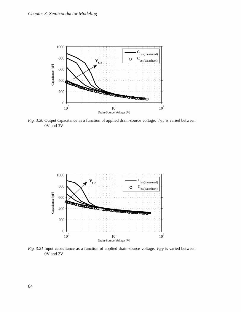
Chapter 3. Semiconductor Modeling
100
101
102
0
200
400
600
800
1000
C
oss(measured)
Coss(datasheet)V
GS
Drain-Source Voltage [V]
Cap
acita
nce
[pF
]
Fig. 3.20Output capacitance as a function of applied drain-source voltage.VGS is varied between0V and 3V
100
101
102
0
200
400
600
800
1000
C
iss(measured)
Ciss(datasheet)
VGS
Drain-Source Voltage [V]
Cap
acita
nce
[pF
]
Fig. 3.21Input capacitance as a function of applied drain-source voltage.VGS is varied between0V and 2V
64

3.3. A Novel MOSFET Model Based on Circuit Analysis
100
101
102
0
200
400
600
800
1000
C
rss(measured)
Crss(datasheet)
VGS
Drain-Source Voltage [V]
Cap
acita
nce
[pF
]
Fig. 3.22Reverse transfer capacitance as a function of applied drain-source voltage.VGS is variedbetween 0V and 2V
0 10 20 30 40 50 600
500
1000
1500
2000
VGS
Drain-source voltage [V]
Gat
e-dra
in c
apac
itan
ce [
pF
]
Fig. 3.23Graph from article by Deml
This statement is based on the fact that the gate-drain capacitor mainly consists of twocapacitors connected in series; field oxide capacitance (Cfield−oxide) and the depletion ca-pacitance (Cdepletion) in the drift region, see Figure 2.10. A high drain-source voltage (i.e.the MOSFET is in blocking state or during current saturation) results in a small depletioncapacitance (Cdepletion ≪ Cfield−oxide) which gives that the gate-drain capacitance basi-cally consists of the depletion capacitance. When the gate-source voltage increases, theMOSFET will eventually turn on and start to operate in the ohmic region. This gives riseto an accumulation layer under the gate electrode which consequently increases the de-pletion capacitance. The drain terminal basically becomesshorted to the source-terminalwhich results in a gate-drain capacitance that is dominatedby the field oxide capacitance[3].
65

Chapter 3. Semiconductor Modeling
In the article by Deml [75, 76], the gate-drain capacitance is measured by a complex reg-ulated circuit whose construction is out of scope for this thesis. The approach used in thisthesis is to measure the gate-drain capacitance at the highest possible gate-source voltagebefore the MOSFET enters the ohmic region and after this point approximate its valuebased on previous measurements. The final function of how thegate-drain capacitancedepends on the applied voltages (CDG(vGS, vDS)) is depicted in 3.24.
0 5 10 15 20 25 0
5
10
15
20
0
500
1000
VDS [V]
VGS [V]
CG
D[p
F]
Fig. 3.24Gate-drain capacitance as a function of applied drain-source and gate-source voltages.
If a switching event is analyzed in detail, the operating points found during the course ofevents can be plotted in the same graph as the gate-drain capacitance, see Figure 3.25.
0
10
20
30
010
20
0
500
1000
0
10
20
30
010
20
0
500
1000
VDS [V]VDS [V]
VGS [V]VGS [V]
CG
D[p
F]
CG
D[p
F]
Fig. 3.25Gate-drain capacitance as a function of applied drain-source and gate-source voltages.Left: Turn-on event marked as a line. Right: Turn-off event marked as a line
66

3.3. A Novel MOSFET Model Based on Circuit Analysis
The main reason for incorporating the gate-drain capacitoras a function of bothVGS andthe VDS comes from the fact that a switching event is a fairly complexprocedure thatcovers all of the operating areas of a power MOSFET. Figure 3.25 visualizes the factthat as the gate-source voltage increases and reaches the miller-region, an increase ofthe gate-drain capacitance will occur. Hence must this region be thoroughly characterizedwhich in this case is accomplished by incorporating the gate-drain capacitance as functionof all applied voltages. Figure 3.26 shows a simulation results from the Matlab modelwhereCGD is only dependent onVDS as suggested in the datasheet. A small deviancecan be seen in all voltages and currents during the switchingevent. This discrepancy isminimized if the gate-drain capacitance is made dependent on bothVGS andVDS, i.e.CGD = f(VGS, VDS), see Figure 3.27. Both simulations are compared with the SPICEmodel which is proven to show good agreement to real measurements.
Time[µs] Time[µs]
Volta
ge[V
]
Volta
ge[V
] /C
urre
nt[A
]
Fig. 3.26Simulation of switching event whereCGD is a function of onlyVDS according to thedatasheet. Matlab simulations: Solid line. SPICE simulations: Dashed line.
Time[µs]Time[µs]
Volta
ge[V
]
Volta
ge[V
] /C
urre
nt[A
]
Fig. 3.27Simulation of switching event whereCGD is a function of bothVGS andVDS . Matlabsimulations: Solid line. SPICE simulations: Dashed line.
67

Chapter 3. Semiconductor Modeling
As previously mentioned, the gate-source capacitance can be considered almost constant[4] since it mainly consists of the parallel plate capacitorformed by the gate electrode,the substrate and the gate-oxide as a dielectric in between.Since the model proposed inthis thesis only deals with positive voltage applied on the gate-terminal, the gate-sourcecapacitance value is chosen to be extracted from the datasheet. The datasheet capacitancecan be expressed as
CGS = 2.84 · 10−9exp (−0.0011 · VDS) + 3.55 · 10−14exp (−0.056 · VDS)(3.22)
if an exponential function is used. The coefficients are calculated using a curve-fittingprocedure.
100
101
102
0
100
200
300
400
CGS(Curve Fit)
CGS(Datasheet)
VDS [V]
CG
S[p
F]
Fig. 3.28Gate-source capacitance as a function of applied Drain-Source voltage. Exponentialcurve fit (solid line) and datasheet values.
The last capacitor that needs to be extracted is the drain-source capacitor. This capac-itor is determined by the size of the junction area between p-type well and the n-typesubstrate layer which has the same electric potential as thesource. This capacitor showssimilar behavior as the capacitance in the pn-junction; it is therefore chosen to obtain thecv-characteristics from the SPICE model where a body diode is present. In SPICE, thejunction capacitance is calculated as described in (2.6) to(2.11). The parameter values inthese equations are taken from the SPICE model delivered by the manufacturer and canbe found in Table 3.3.
The diode capacitance,Cdiode, as a function of applied drain-source voltage,VDS, can beseen in Figure 3.29. Also, the curve fit taken from SPICE is compared with datasheetvalues which show good agreement.
68

3.3. A Novel MOSFET Model Based on Circuit Analysis
Table 3.3 Parameter values for the internal body diode.
Parameter Source Value UnitIS SPICE 8.70123 · 10−12 AN SPICE 1.18415BV SPICE 100 VISR SPICE IS/2 ACJ0 SPICE 1.909 · 10−10 FVJ SPICE 0.5 VM SPICE 0.395FC SPICE 0.1TT SPICE 1 · 10−7 sVthermal SPICE 25.8 · 10−3 VNR SPICE 2Rrev Approximation 1 · 106 Ω
100
101
102
0
50
100
150
200
C
DS(Curve Fit)
CDS(Datasheet)
VDS [V]
Cdio
de
[pF
]
Fig. 3.29Drain-source capacitance as a function of applied Drain-Source voltage. SPICE equa-tions (solid line) and datasheet values.
69

Chapter 3. Semiconductor Modeling
3.3.4 Switching With Purely Resistive Load
Switching of the MOSFET when the load is purely resistive, e.g. a heating element, canbe considered the simplest case of switching and is selectedas a test circuit for furtheranalysis. A typical schematic is depicted in Fig. 3.30.
Rload
RGVin
VG
Fig. 3.30MOSFET switching circuit with purely resistive load.
Even this fairly simple circuit sets high demands on the included models. This can beillustrated by examining Figure 3.31 that depicts a comparison between simulation andmeasurement results. The measurements were made on a circuit consisting of many strayelements, such as hard-wiring between the components and a wire wound load resistor.
0 1 2 3 4 5
0
10
20
30
40
VDS
VGS
ILoad
Time[µs]
Volta
ge[V
]/C
urre
nt[A
]
Fig. 3.31Switching circuit with hardwired layout and wire-wound load resistor. Measurementssolid line. Simulations dotted line.
The values of these stray elements can to some extent be determined if a simple circuitis analyzed. Johannesson and Fransson [65] states that it ispossible to determine val-ues of the parasitic elements if the circuit is built in a controlled way. A controlled waymeans e.g. that the characteristics of the ingoing components are well specified and thatthe circuit layout can be easily measured in order to calculate the stray capacitances.The switching circuit in Figure 3.31 was not built using any favorable components (e.g.
70

3.3. A Novel MOSFET Model Based on Circuit Analysis
low inductive resistors or capacitors with a well defined model); this makes it virtuallyimpossible to determine the stray elements. Also, by mounting the components on anexperimental board, several significant stray elements areintroduced in e.g. long wiresbetween components. All of these stray elements contributeto the resonance circuit thatis formed in the circuit; the voltage overshoot or resonancefrequency as the MOSFETturns off becomes virtually impossible to calculate due to the many unknown parameters.
These results can be compared with Figure 3.32 that depicts simulation and measure-ment results from a circuit with similar operating conditions but utilizes surface mountedcomponents including a low inductive load resistor mountedon a fabricated PCB withadvantageous layout. One conclusion that can be drawn from these measurements andsimulations is that the properties of the investigated semiconductor, in this case only aMOSFET with a simulation model provided by the manufacturer, results in fairly goodagreement between simulation and real life operation. Thishas mainly to do with the factthat the MOSFET model, in this case the IFR7403 from International Rectifier Corpora-tion, has been adapted to suit a switching event. As explained in Section 2.5.7, the modelof the MOSFET can be a rather complex black-box component consisting of several non-physical elements with the only purpose to model a correct switching behavior. This isnot the intention with the MOSFET model proposed in this thesis.
0 1 2 3 4 5
0
10
20
30
40
VDS
VGS
ILoad
Time[µs]
Volta
ge[V
]/C
urre
nt[A
]
Fig. 3.32Switching circuit with advantageous circuit layout and lowinductive load resistor. Mea-surements solid line. Simulations dotted line.
3.3.5 Comparison of Simulations and Measurements
In order to verify the validity of both the SPICE model and theproposed MOSFET model,results from simulations needs to be compared with measurements. By doing this, it can
71

Chapter 3. Semiconductor Modeling
be seen that the black-box SPICE model provided by the manufacturer shows a switchingbehavior that corresponds rather well with the measurements, see Figures 3.33 to 3.34.
0 0.1 0.2 0.3 0.4 0.5 0.6
0
10
20
30
40
50
60
V
GS
VDS
10⋅Id
1 1.1 1.2 1.3 1.4 1.5 1.6
0
10
20
30
40
50
60
V
GS
VDS
10⋅Id
Time[µs]Time[µs]
Volta
ge[V
]/C
urre
nt[A
]
Volta
ge[V
]/C
urre
nt[A
]
Fig. 3.33Switching circuit with IRF520N (Rgate = 110Ω, Rload = 33Ω, Vbat = 60V , Vpulse =12V ). Measurements: solid line. SPICE simulations: dashed line.
0.1 0.2 0.3 0.4 0.5 0.6 0.7
0
5
10
15
20
25
30
V
GS
VDS
Id
1 1.1 1.2 1.3 1.4 1.5 1.6
0
5
10
15
20
25
30
V
GS
VDS
Id
Time[µs]Time[µs]
Volta
ge[V
]/C
urre
nt[A
]
Volta
ge[V
]/C
urre
nt[A
]
Fig. 3.34Switching circuit with IRF520N (Rgate = 110Ω, Rload = 3.7Ω, Vbat = 25V , Vpulse =15V ). Measurements: solid line. SPICE simulations: dashed line.
The most noticeable difference comes from the turn-off procedure. As the gate-sourcevoltage reaches the miller-region and levels out, the drain-source voltage starts to fall. Inthe measurement, this event takes much shorter time which might be caused by a differ-ence in the gate-drain capacitance as the MOSFET turns off. Figure 3.35 and 3.36 shows acomparison between measurements and simulations with the proposed MOSFET model,
72
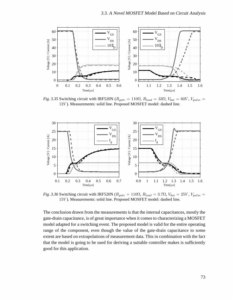
3.3. A Novel MOSFET Model Based on Circuit Analysis
0 0.1 0.2 0.3 0.4 0.5 0.6
0
10
20
30
40
50
60
V
GS
VDS
10⋅ID
1 1.1 1.2 1.3 1.4 1.5 1.6
0
10
20
30
40
50
60
V
GS
VDS
10⋅ID
Time[µs]Time[µs]
Volta
ge[V
]/C
urre
nt[A
]
Volta
ge[V
]/C
urre
nt[A
]
Fig. 3.35Switching circuit with IRF520N (Rgate = 110Ω, Rload = 33Ω, Vbat = 60V , Vpulse =12V ). Measurements: solid line. Proposed MOSFET model: dashedline.
0.1 0.2 0.3 0.4 0.5 0.6 0.7
0
5
10
15
20
25
30
V
GS
VDS
Id
0.9 1 1.1 1.2 1.3 1.4 1.5 1.6
0
5
10
15
20
25
30
V
GS
VDS
Id
Time[µs]Time[µs]
Volta
ge[V
]/C
urre
nt[A
]
Volta
ge[V
]/C
urre
nt[A
]
Fig. 3.36Switching circuit with IRF520N (Rgate = 110Ω, Rload = 3.7Ω, Vbat = 25V , Vpulse =15V ). Measurements: solid line. Proposed MOSFET model: dashedline.
The conclusion drawn from the measurements is that the internal capacitances, mostly thegate-drain capacitance, is of great importance when it comes to characterizing a MOSFETmodel adapted for a switching event. The proposed model is valid for the entire operatingrange of the component, even though the value of the gate-drain capacitance to someextent are based on extrapolations of measurement data. This in combination with the factthat the model is going to be used for deriving a suitable controller makes is sufficientlygood for this application.
73

Chapter 3. Semiconductor Modeling
74

Chapter 4
Active Gate Control and ControllerDesign
4.1 Active Gate Control - Theoretical Derivation
As described in Section 2.6.4, several methods have throughout time been proposed wherethe electromagnetic interference from a switched DC/DC converter is reduced by con-trolling the gate-source voltage. In this section, a new wayof controlling the EMI froma switched DC/DC converter by active gate control is proposed. The main idea behindthe operation principle is that the gate voltage is controlled in such a way that that theharmonic content in the desired output, either drain-source voltage or drain current, is re-duced. The proposed way to do this is by reducing the sharp transitions in the output. Thismethod shall not be mixed up with the traditional method of increasing the gate resistancewhich in a way also accomplishes a lowered harmonic content.Active gate control canlower the harmonic content but also decrease the losses as described in [82].
Instead of using a trapezoidal shaped (can be seen as a squarewave voltage with a finiterise time) gate voltage to switch the semiconductor, it is possible to control the desiredoutput in a more curved way by applying a corresponding gate voltage. The desired outputcan take several shapes, e.g. a sinusoidal transition or a third degree approximation. Themain purpose of this transition and what all applied curveforms should have in commonis the low harmonic content mainly due to rounding off sharp edges and avoiding suddensharp transitions. In this thesis, only the sinusoidal transition is considered. Figure 4.1presents a comparison between a sinusoidal and a trapezoidal transition. The time tracesas well as the resulting frequency spectra is presented.
Figure 4.2 presents a schematic time function,f(t) of the desired voltage waveforms withlinear and sinusoidal transitions.Assume the rise time to betr and the duty cycle to beD, expressed as fractional parts of
75

Chapter 4. Active Gate Control and Controller Design
0 0.1 0.2 0.3 0.4 0.5 0.6 0.7 0.8 0.9 1
0
0.5
1
SinusoidalTrapezoidal
0 10 20 30 40 50
0
0.5
1
104
106
−150
−100
−50
0← f
cutoff = 6.5 kHz
← −40 dB/decade
0 10 20 30 40 50
0
0.5
1
104
106
−150
−100
−50
0← f
cutoff = 10 kHz
← −60 dB/decade
Time [ms]
Time [µs]
Time [µs]
Frequencye [Hz]
Frequencye [Hz]
Am
plitu
de[p
.u.]
Am
plitu
de[p
.u.]
Am
plitu
de[p
.u.]
Am
plitu
de[d
B]
Am
plitu
de[d
B]
Fig. 4.1FFT comparison of pulses with sinusoidal and trapezoidal transitions.
76

4.1. Active Gate Control - Theoretical Derivation
tT/2
tr tf
T/2
A
tT/2
tr tf
T/2
A
Fig. 4.2PWM pulse with sinusoidal and trapezoidal transitions.
the periodT . One period of the functions can be written for the sinusoidal transition as
fsine(t) =
−1 −T2≤ t ≤ t1
f1 = cos[
πtrT
t + π2
(
Dtr− 1
)]
t1 ≤ t ≤ t2
1 t2 ≤ t ≤ t3
f2 = cos[
πtrT
t − π2
(
Dtr− 1
)]
t3 ≤ t ≤ t4
−1 t4 ≤ t ≤ T2
(4.1)
And for the trapezoidal pulse as:
ftrap(t) =
−1 −T2≤ t ≤ t1
f1 = 2trT
t + Dtr
t1 ≤ t ≤ t21 t2 ≤ t ≤ t3f2 = − 2
trTt + D
trt3 ≤ t ≤ t4
−1 t4 ≤ t ≤ T2
(4.2)
wheret1 = (−D − tr)T2, t2 = (−D + tr)
T2, t3 = (D − tr)
T2
andt4 = (D + tr)T2.
The Fourier series expansion for an even function is:
f(t) =a0
2+
∞∑
n=1
an cos(nΩt) (4.3)
77

Chapter 4. Active Gate Control and Controller Design
wherean is determined by
an =4
T
t3∫
0
1 · cos(nΩt)dt +4
T
t4∫
t3
f2 · cos(nΩt)dt + +4
T
T2
∫
t4
−1 · cos(nΩt)dt
After solving and simplifying the expressionan can be written as, for the trapezoidal case:
an =4
π· 1
n2πtr· sin(nπtr) · sin(nπD) (4.4)
an will decrease asn−2 which equals to -40 dB/decade. For the sinusoidal transition func-tion the Fourier component will be given as:
an =−4
π· 1
n((2trn)2 − 1)· cos(nπtr) · sin(nπD) (4.5)
Obviously,an will decrease asn3 for largen. The suspected singularity at(2trn)2 = 1
can be investigated as follows. Consider that
cos(nπtr) = − sin(nπtr −π
2) = − sin
π
2(2ntr − 1) (4.6)
and that
[(2trn)2 − 1] = (2trn + 1)(2trn − 1) (4.7)
Inserting (4.6) and (4.7) in (4.5) gives:
an =4
π· 1
n· 1
(2trn + 1)· π
2· sin π
2(2ntr − 1)
π2(2trn − 1)
· sin(nπD) (4.8)
Since
lim2ntr−1→0
sin π2(2ntr − 1)
π2(2trn − 1)
= 1 (4.9)
an is defined for every value ofn. This results in a theoretical proof of the statement thata sinusoidal transition reduces the harmonic content with -60dB/decade.
4.2 Controller Design
In order to develop a controller that satisfies the demands set by the principle of activegate control, the proposed MOSFET model can be used to deriveappropriate parame-ters. However, the system is strongly nonlinear which meansthat it is not possible toapply straightforward techniques for determining an analytic solution. The common wayof dealing with a nonlinear system equation is to linearize it about an operating point. This
78

4.2. Controller Design
approach gives a reasonably accurate solution for the specified output around a specifiedoperating point. Consider the general nonlinear system
x(t) = f(x(t), u(t))
y(t) = g(x(t), u(t)) (4.10)
wherex(t), u(t) and f are, respectively, then-dimensional system state space vector,the r-dimensional input vector, and then-dimensional vector function. Assume that thenominal (operating) system trajectoryxn(t) is known and that the nominal system inputthat keeps the system on the nominal trajectory is given byfn(t). It can be assumed thatthe actual system dynamics in the immediate proximity of thesystem nominal trajectoriescan be approximated by the first terms of the Taylor series. That is, starting with
x(t) = xn(t) + ∆x(t), u(t) = un(t) + ∆u(t) (4.11)
and
d
dtxn(t) = f(xn(t), un(t)) (4.12)
we expand the right-hand side into the Taylor series as follows
ddt
xn(t) + ddt
∆x(t) = f(xn(t) + ∆x(t), un(t) + ∆u(t)) =
= f(xn + un) +(
∂f
∂x
)
∣
∣
∣
∣
∣
∣
xn(t)
un(t)
∆x +(
∂f
∂u
)
∣
∣
∣
∣
∣
∣
xn(t)
un(t)
∆u + higher order terms (4.13)
Higher-order terms contain at least quadratic quantities of ∆x and∆u. Since they al-ready are small and their squares are even smaller, the high-order terms can be neglected.Neglecting higher-order terms, an approximation is obtained
d
dt∆x(t) =
(
∂f
∂x
)
∣
∣
∣
∣
∣
∣
xn(t)
un(t)
∆x(t) +
(
∂f
∂u
)
∣
∣
∣
∣
∣
∣
xn(t)
un(t)
∆u(t) (4.14)
The partial derivatives represent the Jacobian matrices given by
(
∂f
∂x
)
∣
∣
∣
∣
∣
∣
xn(t)
un(t)
= An×n =
∂f1
∂x1· · · ∂f1
∂xn
......
∂fn
∂x1· · · ∂fn
∂xn
∣
∣
∣
∣
∣
∣
xn(t)
un(t)
(4.15)
79

Chapter 4. Active Gate Control and Controller Design
(
∂f
∂x
)
∣
∣
∣
∣
∣
∣
xn(t)
un(t)
= Bn×r =
∂f1
∂x1· · · ∂f1
∂xn
......
∂fn
∂x1· · · ∂fn
∂xn
∣
∣
∣
∣
∣
∣
xn(t)
un(t)
(4.16)
If the same methodology is applied to then-dimensional vector functiong that governs theoutputs of the system, the expression for the how the outputsbehave around an operatingpoint can be expressed in an analogous way. If the Jacobian matrices are evaluated at thenominal points, that is, atxn(t) andfn(t), the linearized system can be expressed on theform
∆x(t) = A∆x(t) + B∆u(t)
∆y(t) = C∆x(t) + D∆u(t). (4.17)
If a switching event of the proposed MOSFET model is to be simulated, the model needsto be divided into three parts; turned-off region, linear region and the saturated region.Depending on which region the MOSFET operates in, the state matrix A will change, butthe state matrixB will remain the same. When the MOSFET is turned off(iDS = 0), thestate-matrixA becomes
Aoff =
−1CGSRS
1CGSRS
1CGSRS
1CGS
1CGS
0
1CGDRS
−1CGDRS
−1CGDRS
0 −1CGD
0
−1CdiodeRS
1CdiodeRS
−Rrev−RS
CdiodeRrevRS0 0 0
−Ld
Lsum
−Ls
Lsum0 −LsRd−LdRg−LsRg
Lsum0 LsRd−LdRs
Lsum
−Lg
Lsum
Lg+Ls
Lsum0 LsRg−LgRs
Lsum
−LgRd−LsRd−LgRs
Lsum0
−Ld−Lg
Lsum
Lg
Lsum0 LgRd−LdRg
Lsum0 −LgRd−LdRs−LgRs
Lsum
(4.18)
B =
0 0
0 0
0 0
Ld+Ls
Lsum
−Ls
Lsum
−Ls
Lsum
Lg+Ls
Lsum
Ld
Lsum
Lg
Lsum
(4.19)
80

4.2. Controller Design
where
Lsum = LdLg + LdLs + LgLs. (4.20)
For the active and linear region respectively, the state matrix A becomes
Aactive =
−1−2KP ·RS·VCGS0−2KP ·λ·RS·VCd0·VCGS0+2KP ·RS·Vth0+2KP ·λ·RS·VCd0·Vth0
CGSRS1
CGSRS· · ·
1+2KP ·RS·VCGS0+2KP ·λ·RS·VCd0·VCGS0−2KP ·RS·Vth0−2KP ·λ·RS·VCd0·Vth0
CGDRS−1
CGDRS· · ·
−1CdRS
1CdRS
· · ·−Ld
Lsum
−Ls
Lsum· · ·
−Lg
Lsum
Lg+Ls
Lsum· · ·
−Ld−Lg
Lsum
Lg
Lsum· · ·
· · · −1−KP ·λ·RS(VCGS0−Vth0)2
CGSRS1
CGS
1CGS
0
· · · 1+KP ·λ·RS(VCGS0−Vth0)2
CGSRS0 −1
CGD0
· · · −Rrev−RS
CdRrevRS0 0 0
· · · 0 −LsRd−LdRg−LsRg
Lsum0 LsRd−LdRs
Lsum
· · · 0 LsRg−LgRs
Lsum
−LgRd−LsRd−LgRs
Lsum0
· · · 0 LgRd−LdRg
Lsum0 −LgRd−LdRs−LgRs
Lsum
(4.21)
Alinear =
−1+KP ·RS·VCd0+KP ·λ·RS·V 2Cd0
CGSRS1
CGSRS
−2+KP ·RS(3λV 2Cd0
+2(VCGS0−Vth0)+VCd0(2+4λVCGS0−4λVth0)
CGSRS· · ·
1−KP ·RS·VCd0−KP ·λ·RS·V 2Cd0
CGDRS−1
CGDRS
2−KP ·RS(3λV 2Cd0
+2(VCGS0−Vth0)+VCd0(2+4λVCGS0−4λVth0)
CGSRS· · ·
−1CdRS
1CdRS
−Rrev−RS
CdRrevRS· · ·
−Ld
Lsum
−Ls
Lsum0 · · ·
−Lg
Lsum
Lg+Ls
Lsum0 · · ·
−Ld−Lg
Lsum
Lg
Lsum0 · · ·
81

Chapter 4. Active Gate Control and Controller Design
· · · 1CGS
1CGS
0
· · · 0 −1CGD
0
· · · 0 0 0
· · · −LsRd−LdRg−LsRg
Lsum0 LsRd−LdRs
Lsum
· · · LsRg−LgRs
Lsum
−LgRd−LsRd−LgRs
Lsum0
· · · LgRd−LdRg
Lsum0 −LgRd−LdRs−LgRs
Lsum
(4.22)
The step response of the proposed linearized model can be seen in Figure 4.3. In the figure,a small voltage step (3V to 3.1V) is applied on the gate-source terminal of the componentwhen the component is operating in its linear region. The results from SPICE simulationsand the proposed MOSFET model show good agreement both for the gate-source voltageand the drain current, but a small difference can be seen if the linearized model is ana-lyzed. This discrepancy is clearly reasonable due to the linearization around the specifiedoperating point. Several different operating points were analyzed and the conclusion isthat the linearized model shows good agreement with the SPICE model when it comes tosmall signal analysis.
If the linearized model and the SPICE model are verified against real measurements,significantly larger discrepancies can be noticed. Figure 4.4 shows a comparison of mea-surements and SPICE simulations of the small signal response in the active region. Thedifference can mainly be explained due to deviations in static behavior between simulationmodels and real components, see Section 3.3.2 for further explanation and measurements.Due to practical reasons such as internal heating of the component, simulation results arehard to verify with a practical measurement for higher currents.
1 1.1 1.2 1.3
3
3.02
3.04
3.06
3.08
3.1
SpiceFull modelLin. Model
1 1.1 1.2 1.30.03
0.04
0.05
0.06
0.07
0.08
SpiceFull modelLin. Model
Gat
e-S
ourc
eVo
ltage
[V]
Dra
inC
urre
nt[A
]
Time [µs]Time [µs]
Fig. 4.3Comparison of the step response of different MOSFET models.Left: VGS Right: ID
82

4.3. Selecting the output of the system
0 0.5 1 1.54.7
4.75
4.8
4.85
4.9
4.95
SpiceMeasurementLin. Model
0 0.5 1 1.51.5
2
2.5
3
3.5
4
SpiceMeasurementLin. Model
Gat
e-S
ourc
eVo
ltage
[V]
Dra
inC
urre
nt[A
]
Time [µs]Time [µs]
Fig. 4.4Measured step response compared with simulation models. Left: VGS Right: ID
Since this thesis deals with switching procedures, the system will operate in all of thepreceding states. The selected switching needs bo be analyzed and broken down into dis-crete operating points where the first task is to identify which area the model is operatingin. Note that the proposed methodology only gives a rule of thumb when designing thecontroller, when designing a controller that is fully validover the entire operating range,other methods such as exact linearization should be used instead. The method of exactlinearization is described in [77] and a computer based toolis presented in [78].
4.3 Selecting the output of the system
Once the state matrixesA andB are known for all operating points of the system, thematrixes that determine the outputs of the system, matrixesC andD, must be defined.These matrixes do not vary depending on the operating point,but the will differ dependingon the desired output. Basically there are two different signals that can be of interest; thecomponent drain-source voltage and the drain-current (which is the same as the currentthrough the load when the system consists of a purely resistive load). Depending on theoutput, the state-matrixesC andD can be defined as
CVds =[
0 0 0 0 −1 Rd,External
]
(4.23)
DVds =[
0 0]
(4.24)
CId =[
0 0 0 0 1 0]
(4.25)
DId =[
0 0]
(4.26)
83

Chapter 4. Active Gate Control and Controller Design
When the MOSFET is turned off (IDS = 0), a small change in the gate-source voltagewill not affect the desired output in a significant way. This means that the gain of thesystem will be low as seen in Figure 4.5. Also, since it is desired to boost the gate-sourcevoltage to a level just beneath the threshold voltage just before the switching event, thesubthreshold region is of lower importance when the controller is designed. More discus-sions on this topic can be found in Chapter 5 where different methods are considered inorder to optimize the physical implementation of a suitablecontroller.
105
106
107
108
−80
−60
−40
105
106
107
108
0
50
100
frequency [rad/sec]
frequency [rad/sec]
Am
plitu
de
[dB
]P
hase
[Deg
]
Fig. 4.5Bode diagram of the transfer function fromVGS to ID. VGS = 1V andVDS = 25V .
Since the MOSFET are operating under a dynamic procedure, the operating points that thesystem experiences during the switching transient can not be considered as steady statesolutions. Several operating points in the vicinity of the switching event depicted in Figure3.36 were selected and analyzed where an example of the transfer function of the systemoperating in the active region is shown in Figure 4.6 and the ohmic region is shown inFigure 4.7. The bode plots clearly show that the gain of the system depends on the output(drain-source voltage or drain current) which needs to be taken into consideration whendesigning a suitable controller.In order to implement a suitable controller, the system needs to be evaluated in both theohmic and the active region. The problem that inevitably occurs by this transition viathe previously defined stationary points is that the system will enter undefined operatingpoints; the previously analyzed switching event is broken down into some discrete operat-ing points for which the system is defined, but for the area between these points the systemwill still be undefined. In order to get a controller that is suitable for the entire operatingrange, other methods such as exact linearization should be used. However, the purpose ofthis approach is solely to investigate if there is a potential to design a controller on a basis
84

4.3. Selecting the output of the system
105
106
107
108
−10
0
10
20
30
105
106
107
108
−100
−50
0
frequency [rad/sec]
frequency [rad/sec]A
mplitu
de
[dB
]P
hase
[Deg
]
Fig. 4.6Bode diagram of the transfer function fromVGS to ID. VGS = 4.4V andVDS = 25V .
of the obtained parameters and if an adaptive controller gives better performance.
If Figures 4.6 and 4.7 are compared, it can be seen that the gain varies strongly between thetwo operating states. Just as the gate-source voltage exceeds the threshold level, a smallincrease in this voltage gives a large increase in the output, both when the drain-sourcevoltage and the drain current are specified as outputs. Another property of the systemis that the ingoing constants in the state matrixesA, B, C andD varies as the switch-ing event continues. This gives a system with varying properties, see Figure 4.8 wherethe gate-source voltage is increased but kept within the active region. These changes inthe state matrixes as the system is moved along its trajectory can result in two differentscenarios; either can the controller be designed so that it gets exhaustive coverage of alloperating points or it may need adaptive control which is investigated further in Section5.3.
85

Chapter 4. Active Gate Control and Controller Design
105
106
107
108
−60
−40
−20
105
106
107
108
−100
−50
0
frequency [rad/sec]
frequency [rad/sec]
Am
plitu
de
[dB
]P
hase
[Deg
]
Fig. 4.7Bode diagram of the transfer function fromVGS to ID. VGS = 9.5V andVDS = 25V .
105
106
107
108
−10
0
10
20
105
106
107
108
−100
−50
0 VGS
VGS
frequency [rad/sec]
frequency [rad/sec]
Am
plitu
de
[dB
]P
hase
[Deg
]
Fig. 4.8Bode diagram of the transfer function fromVGS to ID. VGS = 4.4V andVDS = 25V .
86

4.3. Selecting the output of the system
The bode plot of the system resembles the bode plot of a first order system; hence cana reasonable approximation be made by translating the low frequency properties of thesystem into a first order system. The transfer function of thetotal system,Gsys, can bewritten as
−4.8e7 · s5 − 1.4e20 · s4 − 1.7e30 · s3 − 7.2e38 · s2 + 2.9e48 · s + 1.2e57
s6 + 2.9e12 · s5 + 7.9e22 · s4 + 5.6e32 · s3 + 4.0e41 · s2 + 7.7e49 · s + 2.2e56(4.27)
which equals a sixth order system. However, the dominant poles of this system can befound at a relatively low frequency, the system can be approximated with a first ordersystem on the form
Gsys =αe
s + αe
. (4.28)
The transfer function in (4.27) can now be expressed as
Gsys =1.47 · 107
s + 2.88 · 106(4.29)
which is a suitable form for designing a controller. Figure 4.9 shows a bode plot com-parison where the difference between the total and the simplified system is shown. Byexpressing the the system as a first order system, the controller design can be significantlysimplified and most important of all; it can be made accordingto the method of loop-shaping which is a special case of the Internal Model Control(IMC) design procedure.This method is thoroughly explained by Harnefors in [79].
105
106
107
108
109
1010
−60
−40
−20
0
20
105
106
107
108
109
1010
−100
−50
0
frequency [rad/sec]
frequency [rad/sec]
Am
plitu
de
[dB
]P
hase
[Deg
]
Fig. 4.9Bode diagram of the transfer function fromVGS to ID. VGS = 4.4V andVDS = 25V .
87

Chapter 4. Active Gate Control and Controller Design
4.4 Controller Design
The basic operating principle of the complete closed loop system including a controlleris depicted in Figure 4.10 where a block diagrams is presented for both the drain currentand the drain-source voltage selected as the controlled quantity.
GSYSFC
IDS* IDSVGS
GSYSFC
VDS* VDSVGS
Fig. 4.10MOSFET switching circuit with purely resistive load.
Since the transfer function of the system,Gsys, can be approximated with a transfer func-tion of order one, the controller,Fc, can b selected as a simple PI-controller; the orderof the controller does not need to be higher than that of the controlled process. The ideais to specify the desired rise time (10% - 90%) of the closed loop system. If the transferfunction of the system,Gsys, is known, it is apparent that the closed loop transfer functionof the total closed loop system depicted in Figure 4.10 can beobtained according to
Gcl(s) =Fc(s)Gsys(s)
1 + Fc(s)Gsys(s), (4.30)
whereGcl is the closed-loop transfer function andFc(s) is the transfer function of thecontroller. In Figure 4.11 the step response of the open loopsystem from a unity stepapplied to the input (VGS) is seen as a solid line. The step response of the system if aunity step is applied results in a large remaining error; an error that can be eliminated byapplying a well designed controller.
By using the IMC-method, a controller can be designed that isvalid around a specifiedoperating point. In order to obtain the closed loop transferfunction in (4.30), the controllerFc(s) must be designed according to
Fc(s) =αe
sG−1
sys(s) (4.31)
whereαe is the desired bandwidth of the total system. A suitable controller for the systemin (4.29) can then be expressed as
Fc(s) =αe
s
(
1.47 · 107
s + 2.88 · 106
)
−1
(4.32)
88

4.4. Controller Design
where the bandwidth is determined byαe. To verify the method, the step response of thesystem can be studied. The dashed line in Figure 4.11 shows how the systemGcl(s) takenfrom (4.29) behaves when a controller circuit with rise time10µs is implemented.
0 5 10 150
0.5
1
1.5
2
2.5
3
3.5
Time [µs]
Volta
ge[V
]
Fig. 4.11Step response of the transfer function fromVGS to VDS . Solid Line: Without controller.Dashed Line: Closed loop system with controller.
The method proposed by IMC works and gives the desired results applied to the system.However, one concern still remains and that is how the changes in system parameters willinfluence the controller design.
89

Chapter 4. Active Gate Control and Controller Design
90

Chapter 5
Implementation of Active Gate Control
In order to realize a control circuit for active gate control, the control strategies that werederived in the previous section are now implemented. A principal schematic of how theproposed controller structure is realized is shown in Figure 5.1 where the magnitude ofthe error depends on which output quantity (VDS or ID) that is desired to control.
Rload
errorR1
R2 C
Fig. 5.1Principal schematic of the controller circuit implementedin SPICE.
According to the reasoning in Section 4.4, a suitable controller would consist of a propor-tional and a integral part, a PI-controller, with the transfer function
Fc(s) = Kp +Ki
s. (5.1)
This controller can be realized with help of operational amplifiers according to the circuitdepicted in Figure 5.1. The proportional gain is determinedby
Kp =R2
R1(5.2)
and the integral gain is determined by
Ki =1
R1C. (5.3)
Note that the circuit in Figure 5.1 produces a negative voltage, hence, an inverting voltagefollower or summer must be attached between the controller circuit and the MOSFET in
91

Chapter 5. Implementation of Active Gate Control
order to obtain a functioning circuit. One other important aspect of the controller designis to guarantee that the output of the operational amplifier can deliver sufficient current.As the gate-source voltage increases above the threshold voltage, a charge of the internalcapacitors will start which causes a high flow of current. Thepeak of this inrush currentis mainly determined by theRC-link formed on the gate terminal of the component andcan consequently be limited by selecting a larger gate resistor.
An FPGA is used to generate the sinusoidal shaped reference waveform [80], see Figure5.2 for a photo of the measurement setup. Due to limitations in the FPGA-circuit, the in-vestigated rise times and switching frequencies are limited to a certain number of discretesteps in order to avoid jitter. The frequencies and rise-times are presented in Table 5.1 andare consequently the subject of investigation for all upcoming measurements.
Table 5.1 Switching frequency and rise-times of the reference waveform.
Frequency Rise Time [%] Rise Time [µs]2464Hz 10% 40.6µs
1% 4.0µs493Hz 10% 202.8µs
1% 20.3µs
Fig. 5.2Photograph of the FPGA reference waveform generator and controller circuit.
According to the reasoning in Section 4.4, the design of the controller circuit can be madeaccording to IMC which requires a small signal analysis around an operating point. Theapproach analyzed in this thesis is based on discretizationof the switching event, bothturn-on and turn-off, where each operating point is analyzed individually to form a con-troller that will vary during the event. The external parameters are chosen correspondinglyto Figure 3.36 whereVbat = 25V , Vgate = 15V andRload = 3.7Ω. The analyzed operatingpoints during the turn-on switching event (for only the electrical circuit system excluding
92

5.1. Step Response of the System
the controller circuit) are shown as circles in Figure 5.3, in total 16points excluding thesubthreshold region. In all forthcoming reasoning, the operating points that are discussedrefers to this figure.
0.2 0.3 0.4 0.5 0.6
0
5
10
15
20
25
V
GS
VDS
Operating Point
Point 1
Time [µs]
Volta
ge[V
]
Fig. 5.3Proportional and integral gain variations for a suitable controller during a switching event.
5.1 Step Response of the System
In order to evaluate the closed loop system, the step response of the system is evaluated.The entire switching event is discretized into operating points, each evaluated separately.Figure 5.4 shows all analyzed operating points (in total 16points excluding the subthresh-old region) for only the electrical circuit system during turn-on excluding the controllercircuit. The variations in both the proportional gain (Kp) and integral gain (Ki) for theanalyzed switching event with a resulting rise-time of 4µs are shown on the right axis inFigures 5.4 and 5.5. The same analysis was performed to the turn-off event even thoughthe discretized event is not shown here.
Based on measurements and simulations for the current operating case and for all rise-times specified in Table 5.1, it can be concluded that the mostsuitable controller withfixed parameters is always the one derived from the beginningof the turn-on event (point1 in Figure 5.4). If controllers from the following operating points are used (i.e. points2 and up in Figure 5.4), the step response becomes highly distorted. The most probableexplanation of this relationship is that the integral gain of the controller becomes toolarge in order to initialize the switching event. This is illustrated in Figure 5.6 where thestep response for the system including a mathematically derived controller for the firstoperating points in the active region is shown. The simulation results from the SPICEmodel and the proposed simulink model show good agreement.
93

Chapter 5. Implementation of Active Gate Control
0.1 0.2 0.3 0.4 0.5 0.6
0
10
20
30
0.1 0.2 0.3 0.4 0.5 0.6
0
1
2GainV
GS
VDS
0.1 0.2 0.3 0.4 0.5 0.6
0
10
20
30
0.1 0.2 0.3 0.4 0.5 0.6
0
1
2x 10
7
GainV
GS
VDS
ActiveRegion
ActiveRegion
Time [µs]
Time [µs]
Volta
ge[V
]
Pro
port
iona
lGai
n
Volta
ge[V
]
Inte
gral
Gai
n
Fig. 5.4Proportional and integral gain variations for a controllerwith trise = 4µs during a switch-ing event,iDS selected as output.
0.1 0.2 0.3 0.4 0.5 0.6
0
10
20
30
0.1 0.2 0.3 0.4 0.5 0.6
0
1
2GainV
GS
VDS
0.1 0.2 0.3 0.4 0.5 0.6
0
10
20
30
0.1 0.2 0.3 0.4 0.5 0.6
0
1
2x 10
7
GainV
GS
VDS
ActiveRegion
ActiveRegion
Time [µs]
Time [µs]
Volta
ge[V
]
Pro
port
iona
lGai
n
Volta
ge[V
]
Inte
gral
Gai
n
Fig. 5.5Proportional and integral gain variations for a controllerwith trise = 4µs during a switch-ing event,vDS selected as output.
94

5.1. Step Response of the System
Also worth noticing in Figure 5.6 is the difference between the real rise time (≈ 1.5µs)which is significantly faster than the desired rise time (4µs). This discrepancy is seen forall rise times specified in Table 5.1 and is most likely explained by the change in the in-going parameters as the switching event proceeds; a controller derived for the initiationof the switching event is not suitable any longer at the end ofthe switching event due tochanges in the system parameters such asCGD.
0 1 2 3 4 5−1
0
1
2
3
4
5
6
7
vreference
VGS, spice
VGS, simulink
0 1 2 3 4 5−1
0
1
2
3
4
5
6
7
vreference
VGS, spice
VGS, simulink
Increasingoperating point
Increasingoperating point
Volta
ge[V
]/C
urre
nt[A
]
Volta
ge[V
]/C
urre
nt[A
]
Time [µs]Time [µs]
Fig. 5.6Simulated step response with derived controller structures.Id selected as output, step from0A to 6A. 4µs desired rise time. Note that the dashed line is not visible due to overlapping.
0 1 2 3 4 5−1
0
1
2
3
4
5
6
7
vref, measured
VGS, measured
0 1 2 3 4 5−1
0
1
2
3
4
5
6
7
vref, measured
IDS, measured
Increasingoperating point
Increasingoperating point
Volta
ge[V
]/C
urre
nt[A
]
Volta
ge[V
]/C
urre
nt[A
]
Time [µs]Time [µs]
Fig. 5.7Measured step response with derived controller structures. Id selected as output, step from0A to 6A. 4µs desired rise time.
The previously derived simulation results are also valid for real measurements, see Figure5.7 which shows the measurement results for the same operating conditions as in Figure5.7. Once again, the difference in static behavior between the simulation models and themeasurements can be noted, see Section 3.3.2. Here is it foremost seen as a difference in
95
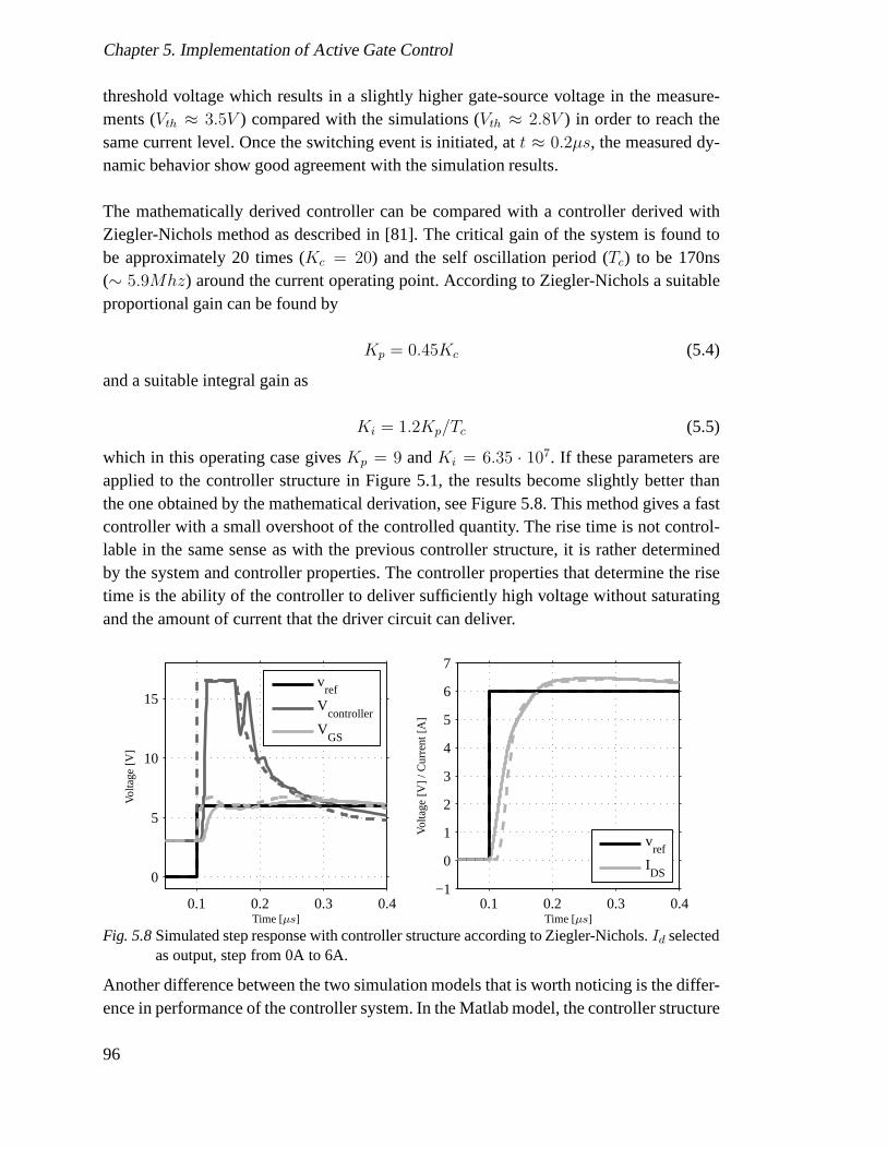
Chapter 5. Implementation of Active Gate Control
threshold voltage which results in a slightly higher gate-source voltage in the measure-ments (Vth ≈ 3.5V ) compared with the simulations (Vth ≈ 2.8V ) in order to reach thesame current level. Once the switching event is initiated, at t ≈ 0.2µs, the measured dy-namic behavior show good agreement with the simulation results.
The mathematically derived controller can be compared witha controller derived withZiegler-Nichols method as described in [81]. The critical gain of the system is found tobe approximately 20 times (Kc = 20) and the self oscillation period (Tc) to be 170ns(∼ 5.9Mhz) around the current operating point. According to Ziegler-Nichols a suitableproportional gain can be found by
Kp = 0.45Kc (5.4)
and a suitable integral gain as
Ki = 1.2Kp/Tc (5.5)
which in this operating case givesKp = 9 andKi = 6.35 · 107. If these parameters areapplied to the controller structure in Figure 5.1, the results become slightly better thanthe one obtained by the mathematical derivation, see Figure5.8. This method gives a fastcontroller with a small overshoot of the controlled quantity. The rise time is not control-lable in the same sense as with the previous controller structure, it is rather determinedby the system and controller properties. The controller properties that determine the risetime is the ability of the controller to deliver sufficientlyhigh voltage without saturatingand the amount of current that the driver circuit can deliver.
0.1 0.2 0.3 0.4
0
5
10
15
v
ref
Vcontroller
VGS
0.1 0.2 0.3 0.4−1
0
1
2
3
4
5
6
7
vref
IDS
Volta
ge[V
]
Volta
ge[V
]/C
urre
nt[A
]
Time [µs]Time [µs]
Fig. 5.8Simulated step response with controller structure according to Ziegler-Nichols.Id selectedas output, step from 0A to 6A.
Another difference between the two simulation models that is worth noticing is the differ-ence in performance of the controller system. In the Matlab model, the controller structure
96
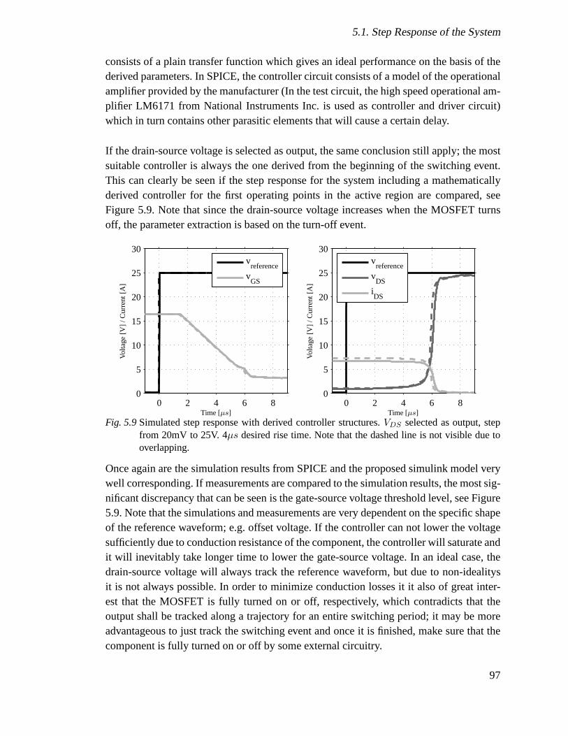
5.1. Step Response of the System
consists of a plain transfer function which gives an ideal performance on the basis of thederived parameters. In SPICE, the controller circuit consists of a model of the operationalamplifier provided by the manufacturer (In the test circuit,the high speed operational am-plifier LM6171 from National Instruments Inc. is used as controller and driver circuit)which in turn contains other parasitic elements that will cause a certain delay.
If the drain-source voltage is selected as output, the same conclusion still apply; the mostsuitable controller is always the one derived from the beginning of the switching event.This can clearly be seen if the step response for the system including a mathematicallyderived controller for the first operating points in the active region are compared, seeFigure 5.9. Note that since the drain-source voltage increases when the MOSFET turnsoff, the parameter extraction is based on the turn-off event.
0 2 4 6 80
5
10
15
20
25
30
v
reference
vGS
0 2 4 6 80
5
10
15
20
25
30
v
reference
vDS
iDS
Volta
ge[V
]/C
urre
nt[A
]
Volta
ge[V
]/C
urre
nt[A
]
Time [µs]Time [µs]
Fig. 5.9Simulated step response with derived controller structures. VDS selected as output, stepfrom 20mV to 25V. 4µs desired rise time. Note that the dashed line is not visible due tooverlapping.
Once again are the simulation results from SPICE and the proposed simulink model verywell corresponding. If measurements are compared to the simulation results, the most sig-nificant discrepancy that can be seen is the gate-source voltage threshold level, see Figure5.9. Note that the simulations and measurements are very dependent on the specific shapeof the reference waveform; e.g. offset voltage. If the controller can not lower the voltagesufficiently due to conduction resistance of the component,the controller will saturate andit will inevitably take longer time to lower the gate-sourcevoltage. In an ideal case, thedrain-source voltage will always track the reference waveform, but due to non-idealitysit is not always possible. In order to minimize conduction losses it it also of great inter-est that the MOSFET is fully turned on or off, respectively, which contradicts that theoutput shall be tracked along a trajectory for an entire switching period; it may be moreadvantageous to just track the switching event and once it isfinished, make sure that thecomponent is fully turned on or off by some external circuitry.
97

Chapter 5. Implementation of Active Gate Control
0 2 4 6 80
5
10
15
20
25
30
v
ref, measured
vGS, measured
0 2 4 6 80
5
10
15
20
25
30
v
ref, measured
vDS, measured
iDS, measured
Volta
ge[V
]/C
urre
nt[A
]
Volta
ge[V
]/C
urre
nt[A
]
Time [µs]Time [µs]
Fig. 5.10Measured step response with derived controller structures. VDS selected as output, stepfrom 20mV to 25V. 4µs desired rise time.
Another problem that will appear when the drain source-voltage is selected as output isthe delay that occurs before the voltage start to rise. This delay originates from severalfactors parts; the delay in the controller circuit and the speed of the controller whichaffects the time it takes for the controller to lower the gatevoltage to reach the Millerregion. Measurements shows the same results and verify the simulations, see Figure 5.10.One way to minimize the problem is to slow down the controller, but simulations showsthat the delay will always cause some delay in the circuit before the drain-source voltagestarts to rise.
5.2 Sinusoidal Step Response of the System
In order to implement active gate control, not only the step response of the system needsto be evaluated, the behavior when a applying a sinusoidal reference waveform also needsto be analyzed. Figure 5.11 shows the simulated response of the system withIDS selectedas output when a sinusoidal reference with 4µs rise time is applied. It can be concludedthat the SPICE model gives more accurate results compared with measurements due tothe delay in the controller. The simulink model gives a similar step response but slightlyfaster due to the lack of delay. Measurements show that the SPICE model shows goodaccuracy, see Figure 5.12 where the same sinusoidal step is applied as reference voltage.Also, if a controller with parameters derived by the ZieglerNichols method is simulated,a slightly better result is obtained, see Figure 5.13, the controller is s
98

5.2. Sinusoidal Step Response of the System
0 2 4 6 8 10−1
0
1
2
3
4
5
6
7
vreference
vGS, spice
vGS, simulink
0 2 4 6 8 10−1
0
1
2
3
4
5
6
7
vreference
iDS, spice
iDS, simulink
Volta
ge[V
]
Volta
ge[V
]/C
urre
nt[A
]
Time [µs]Time [µs]
Fig. 5.11Simulation results with sinusoidal reference,trise = 4µs. Id selected as output.
0 2 4 6 8 10−1
0
1
2
3
4
5
6
7
ylab
el
vref, measured
VGS, measured
0 2 4 6 8 10−1
0
1
2
3
4
5
6
7
ylab
el
vref, measured
IDS, measured
Time [µs]Time [µs]
Fig. 5.12Measurement results with sinusoidal reference,trise = 4µs. Id selected as output.
0 2 4 6−1
0
1
2
3
4
5
6
7
vreference
vGS, spice
vGS, simulink
0 2 4 6−1
0
1
2
3
4
5
6
7
vreference
iDS, spice
iDS, simulink
Volta
ge[V
]
Volta
ge[V
]/C
urre
nt[A
]
Time [µs]Time [µs]
Fig. 5.13Simulation results with sinusoidal reference, Ziegler-Nichols controller,trise = 4µs. Id
selected as output.
99

Chapter 5. Implementation of Active Gate Control
If the sinusoidal step response withVDS selected as output, the previously mentioned de-lay becomes even more significant, see Figure 5.14. In this case has delay not so muchto do with the internal delay in the controller circuit as it has to do with the time it takesfor the controller to respond and lower the gate-source voltage to a suitable level. Thisdelay was also observed by Holst and Futane in [2], their approach was to implement anexternal circuitry that pre-charges (or pre-discharges) the gate-source voltage just beforethe moment of transition. Also, a rather big discrepancy canbe seen SPICE results andthe results obtained by the Matlab model. This deviance mostlikely origin from an inad-equate description in the gate-drain capacitance for the off transition.
0 2 4 6 8
0
10
20
30
40 vreference
vGS
0 2 4 6 8
0
10
20
30
40 vreference
iDS
vDS
Volta
ge[V
]
Volta
ge[V
] /C
urre
nt[A
]
Time [µs]Time [µs]
Fig. 5.14Simulation results with sinusoidal reference,trise = 4µs. vDS selected as output.
0 2 4 6 80
10
20
30
40
ylab
el
v
ref, measured
VGS, measured
0 2 4 6 80
10
20
30
40
ylab
el
v
ref, measured
iDS, measured
vDS, measured
Time [µs]Time [µs]
Fig. 5.15Measurement results with sinusoidal reference,trise = 4µs. vDS selected as output.
The results presented in [2, 82] showed that a slight improvement is possible by precharg-ing the gate of the MOSFET. This investigation was performedat an early stage of the
100
5.3. Controller Design With Varying Parameters
project and it was decided that a more theoretical approach was to be investigated, hence,this thesis was focused on semiconductor modeling and deriving suitable controller pa-rameters instead. The external precharging circuitry increased the cost and the complexityof the circuit and made it rather sensitive to changes in operating conditions, e.g. supplyvoltage and reference voltage variations. All in all, the technique of external prechargingwas considered not worth investigating further due to thesedisadvantages.
Although an external precharging was found to be too complex, the idea can still beadapted to modern technology such as digital control. In order to make precharging moreversatile and suitable for this type of system it can be of interest to completely imple-ment the precharging circuitry within a digital controller. By doing this, the gate controlis entirely embedded in an digital environment which facilitates both adaptive control (seenext section) and removes the need for external circuitry that increases/decreases the gate-source voltage once the transition has been passed. However, this kind of digital controlis out of scope of this thesis and can be considered to be an interesting subject for furtherinvestigations.
Based on simulations and measurements it is concluded that the drain-source voltage ishard to control due to several reasons. The foremost disadvantage when controlling thedrain-source voltage is to adjust the reference voltage to the current operating conditions.This means that when the MOSFET is fully conducting, the voltage drop that becomespresent over the component must be accounted for when comparing the measured voltagewith the reference voltage. If these two voltages does not correspond, i.e. the referencevoltage is lower than the measured voltage, the controller will saturate. The forward volt-age drop over the MOSFET depends on several factors where thegate-source voltage isone of them. Also, in addition to finding the low level of the reference voltage, the highlevel also needs to be adjusted depending on the operating conditions (i.e. supply volt-age). Parts of this reasoning are of course also valid when controlling the drain current;the main difference is that when the MOSFET is turned off, thedrain current also goes tozero which gives no need for adjusting the reference voltagelevel during this time. Hence,all further investigations focused on controlling the drain current.
5.3 Controller Design With Varying Parameters
The controller designed with the proposed method must be valid over the entire operat-ing range of the MOSFET, all parameter (e.g.CGD) variations included. The reasoning inprevious sections have shown that the parameter variationsare too big for the controller tohandle. This gives the need for adaptive design of the controller parameters; i.e. the con-troller parameters shall be adapted during the switching transition itself in order to bettersuit the system. This section is entirely based on theoretical reasoning and simulations
101
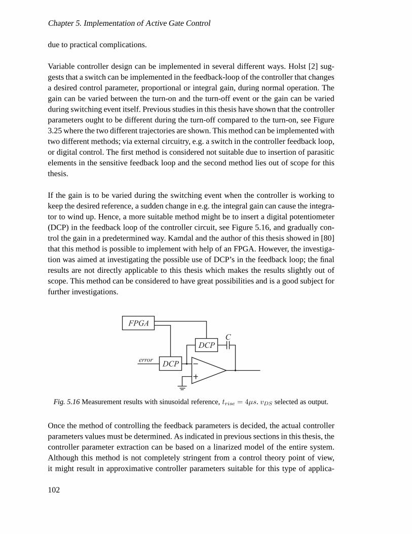
Chapter 5. Implementation of Active Gate Control
due to practical complications.
Variable controller design can be implemented in several different ways. Holst [2] sug-gests that a switch can be implemented in the feedback-loop of the controller that changesa desired control parameter, proportional or integral gain, during normal operation. Thegain can be varied between the turn-on and the turn-off eventor the gain can be variedduring switching event itself. Previous studies in this thesis have shown that the controllerparameters ought to be different during the turn-off compared to the turn-on, see Figure3.25 where the two different trajectories are shown. This method can be implemented withtwo different methods; via external circuitry, e.g. a switch in the controller feedback loop,or digital control. The first method is considered not suitable due to insertion of parasiticelements in the sensitive feedback loop and the second method lies out of scope for thisthesis.
If the gain is to be varied during the switching event when thecontroller is working tokeep the desired reference, a sudden change in e.g. the integral gain can cause the integra-tor to wind up. Hence, a more suitable method might be to insert a digital potentiometer(DCP) in the feedback loop of the controller circuit, see Figure 5.16, and gradually con-trol the gain in a predetermined way. Kamdal and the author ofthis thesis showed in [80]that this method is possible to implement with help of an FPGA. However, the investiga-tion was aimed at investigating the possible use of DCP’s in the feedback loop; the finalresults are not directly applicable to this thesis which makes the results slightly out ofscope. This method can be considered to have great possibilities and is a good subject forfurther investigations.
error
DCPC
DCP
FPGA
Fig. 5.16Measurement results with sinusoidal reference,trise = 4µs. vDS selected as output.
Once the method of controlling the feedback parameters is decided, the actual controllerparameters values must be determined. As indicated in previous sections in this thesis, thecontroller parameter extraction can be based on a linarizedmodel of the entire system.Although this method is not completely stringent from a control theory point of view,it might result in approximative controller parameters suitable for this type of applica-
102
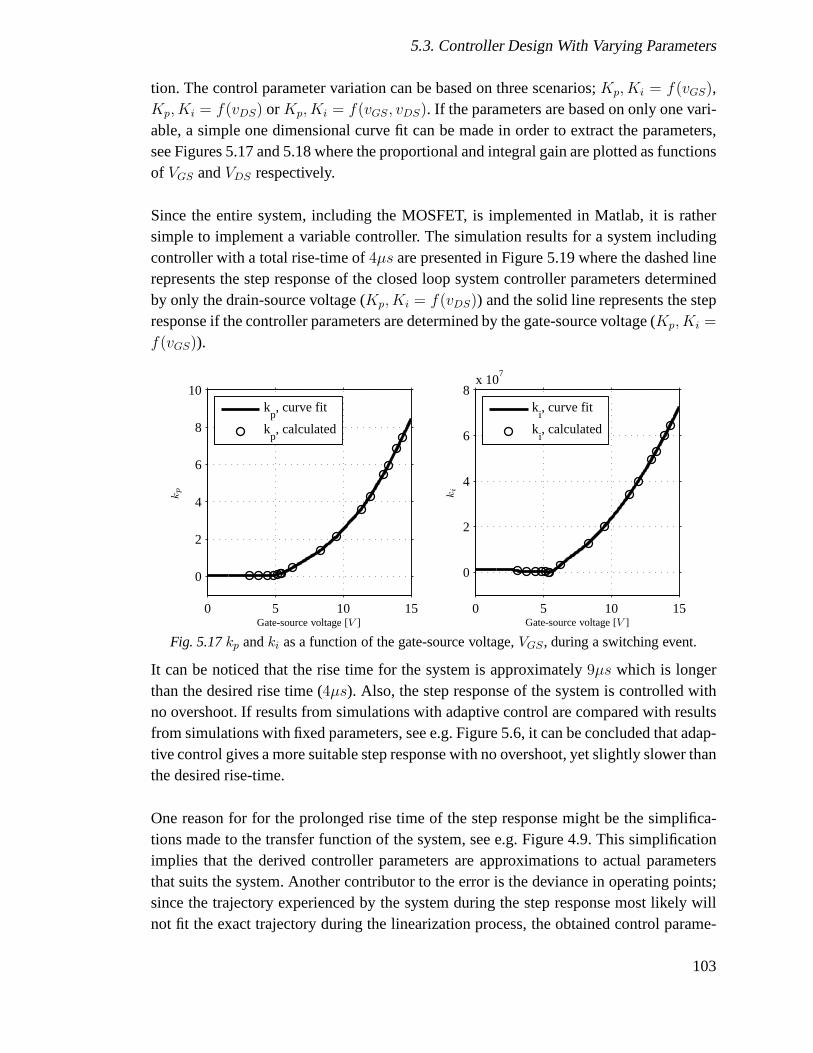
5.3. Controller Design With Varying Parameters
tion. The control parameter variation can be based on three scenarios;Kp, Ki = f(vGS),Kp, Ki = f(vDS) or Kp, Ki = f(vGS, vDS). If the parameters are based on only one vari-able, a simple one dimensional curve fit can be made in order toextract the parameters,see Figures 5.17 and 5.18 where the proportional and integral gain are plotted as functionsof VGS andVDS respectively.
Since the entire system, including the MOSFET, is implemented in Matlab, it is rathersimple to implement a variable controller. The simulation results for a system includingcontroller with a total rise-time of4µs are presented in Figure 5.19 where the dashed linerepresents the step response of the closed loop system controller parameters determinedby only the drain-source voltage (Kp, Ki = f(vDS)) and the solid line represents the stepresponse if the controller parameters are determined by thegate-source voltage (Kp, Ki =
f(vGS)).
0 5 10 15
0
2
4
6
8
10
k
p, curve fit
kp, calculated
0 5 10 15
0
2
4
6
8x 10
7
k
i, curve fit
ki, calculated
kp ki
Gate-source voltage [V ] Gate-source voltage [V ]
Fig. 5.17kp andki as a function of the gate-source voltage,VGS , during a switching event.
It can be noticed that the rise time for the system is approximately9µs which is longerthan the desired rise time (4µs). Also, the step response of the system is controlled withno overshoot. If results from simulations with adaptive control are compared with resultsfrom simulations with fixed parameters, see e.g. Figure 5.6,it can be concluded that adap-tive control gives a more suitable step response with no overshoot, yet slightly slower thanthe desired rise-time.
One reason for for the prolonged rise time of the step response might be the simplifica-tions made to the transfer function of the system, see e.g. Figure 4.9. This simplificationimplies that the derived controller parameters are approximations to actual parametersthat suits the system. Another contributor to the error is the deviance in operating points;since the trajectory experienced by the system during the step response most likely willnot fit the exact trajectory during the linearization process, the obtained control parame-
103

Chapter 5. Implementation of Active Gate Control
0 5 10 15 20
0
2
4
6
8
k
p, curve fit
kp, calculated
0 5 10 15 20−1
0
1
2
3
4
5x 10
7
k
i, curve fit
ki, calculated
kp ki
Drain-source voltage [V ] Drain-source voltage [V ]
Fig. 5.18kp andki as a function of the drain-source voltage,VDS , during a switching event.
5 10 15 20 25 30−1
0
1
2
3
4
5
6
7
vreference
vGS
5 10 15 20 25 30
0
5
10
15
20
25
v
reference
vDS
iDS
Volta
ge[V
]
Volta
ge[V
]/C
urre
nt[A
]
Time [µs]Time [µs]
Fig. 5.19Measured step response with variable controller structures. Id selected as output, stepfrom 0A to 6A. 4µs desired rise time. Dashed line:Kp,Ki = f(vDS). Solid line:Kp,Ki = f(vGS)
ters can be inadequate. This divergence is a well known shortcoming with the proposedmethodology as explained in previous sections.
In order overcome, or at least minimize, the problem with finding suitable controller pa-rameters when the proportional and integral gain changes during a switching event, thetwo controller parameters can be made dependent on two variables,Kp, Ki = f(vGS, vDS).In Figure 5.20, three different switching trajectories areshown as a function ofvDS andvGS. Each switching trajectory are valid for the investigated system with different externalvoltages applied, i.e. the supply voltagevDS and the peak value ofvGS is changed.
Based on these three switching trajectories obtained by simulations of the system without
104

5.3. Controller Design With Varying Parameters
05
1015
2025 4 6 8 10 12 14
0
5
10
Drain-source voltage [V ] Gate-source voltage [V ]
kp
Fig. 5.20kp as a function of both drain-source and gate-source voltage during a turn-on event.Three different switching trajectories.
controller, the proportional and integral gain can be calculated in several discrete oper-ating points in the vicinity of the trajectory. This is exactly the same methodology asdescribed in Figure 5.3, but adapted for three different operating conditions. Based onthese trajectories, an approximative surface can be created from which the approximativegain, both proportional and integral, can be interpolated for all operating points that thesystem may experience, see Figure 5.21 forkp-surface and 5.22 forki-surface. Once againit shall be noted that this methodology is not completely stringent from a control theorypoint of view; the obtained gains shall rather be seen as a rule of thumb.
05
1015
2025
5
10
150
5
10
Drain-source voltage [V ]Gate-source voltage [V ]
kp
Fig. 5.21Interpolated surface forkp as a function of both drain-source and gate-source voltageduring a turn-on event.
105
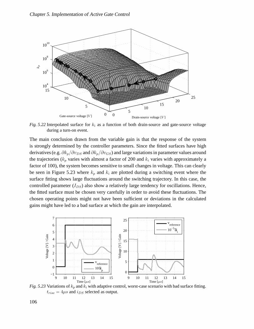
Chapter 5. Implementation of Active Gate Control
05
1015
2025
0
5
10
1510
4
106
108
1010
Drain-source voltage [V ]Gate-source voltage [V ]
kp
Fig. 5.22Interpolated surface forki as a function of both drain-source and gate-source voltageduring a turn-on event.
The main conclusion drawn from the variable gain is that the response of the systemis strongly determined by the controller parameters. Sincethe fitted surfaces have highderivatives (e.g.∂kp/∂vDS and∂kp/∂vGS) and large variations in parameter values aroundthe trajectories (kp varies with almost a factor of 200 andki varies with approximately afactor of 100), the system becomes sensitive to small changes in voltage. This can clearlybe seen in Figure 5.23 wherekp andki are plotted during a switching event where thesurface fitting shows large fluctuations around the switching trajectory. In this case, thecontrolled parameter (IDS) also show a relatively large tendency for oscillations. Hence,the fitted surface must be chosen very carefully in order to avoid these fluctuations. Thechosen operating points might not have been sufficient or deviations in the calculatedgains might have led to a bad surface at which the gain are interpolated.
9 10 11 12 13 14 15−1
0
1
2
3
4
5
6
7
vreference
10⋅kp
9 10 11 12 13 14 15
0
5
10
15
20
25
v
reference
10−5⋅ki
Volta
ge[V
]/G
ain
Volta
ge[V
]/G
ain
Time [µs]Time [µs]
Fig. 5.23Variations ofkp andki with adaptive control, worst-case scenario with bad surface fitting.trise = 4µs andiDS selected as output.
106
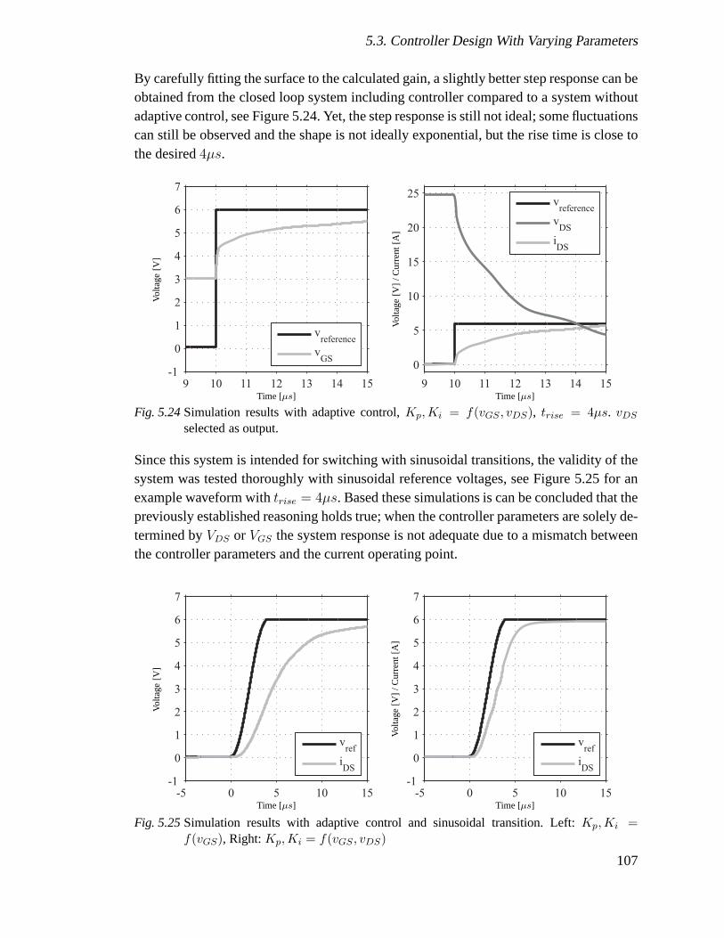
5.3. Controller Design With Varying Parameters
By carefully fitting the surface to the calculated gain, a slightly better step response can beobtained from the closed loop system including controller compared to a system withoutadaptive control, see Figure 5.24. Yet, the step response isstill not ideal; some fluctuationscan still be observed and the shape is not ideally exponential, but the rise time is close tothe desired4µs.
9 10 11 12 13 14 15-1
0
1
2
3
4
5
6
7
vreference
vGS
9 10 11 12 13 14 15
0
5
10
15
20
25v
reference
vDS
iDS
Volta
ge[V
]
Volta
ge[V
] /C
urre
nt[A
]Time [µs]Time [µs]
Fig. 5.24Simulation results with adaptive control,Kp,Ki = f(vGS , vDS), trise = 4µs. vDS
selected as output.
Since this system is intended for switching with sinusoidaltransitions, the validity of thesystem was tested thoroughly with sinusoidal reference voltages, see Figure 5.25 for anexample waveform withtrise = 4µs. Based these simulations is can be concluded that thepreviously established reasoning holds true; when the controller parameters are solely de-termined byVDS or VGS the system response is not adequate due to a mismatch betweenthe controller parameters and the current operating point.
-5 0 5 10 15-1
0
1
2
3
4
5
6
7
vref
iDS
-5 0 5 10 15-1
0
1
2
3
4
5
6
7
vref
iDS
Volta
ge[V
]
Volta
ge[V
] /C
urre
nt[A
]
Time [µs]Time [µs]
Fig. 5.25Simulation results with adaptive control and sinusoidal transition. Left: Kp,Ki =f(vGS), Right:Kp,Ki = f(vGS , vDS)
107

Chapter 5. Implementation of Active Gate Control
An example of this deviance can be seen Figure 5.25, left picture, where a sinusoidalreference voltage withtrise = 4µs is applied to a system withKp, Ki = f(vGS). Bymaking the controller parameters dependent on bothVDS or VGS, the system response getsslightly better, see Figure 5.25, right picture, whereKp, Ki = f(vGS, vDS). Once again,the controller parameters from the fitted surface does not entirely match the analyticallyobtained values for the current trajectory which can be seenas a small superimposedoscillation onIDS.
5.4 Robustness of the Circuit
In order to evaluate the system stability and usefulness it is important to verify the circuitin different operating conditions. Until now, only one operating case has been evaluated;this section deals with problems that can arise the the operating conditions are changedand discussions regarding the system versatility. As previously discussed, it if found moreadvantageous to control the drain current than the drain-source voltage. By doing this,only one voltage level of the waveform has to be varied if the supply voltage changes.This is illustrated in Figure 5.26 where three different simulations with varying supplyvoltage are presented. As seen, only one of these voltages (25V) result in a correct shapeof the controlled quantity. For the other two cases, 17V and 22V, the reference voltage islo longer adapted to the maximum drain current which causes the controller to saturateand the controlled quantity be distorted. For reasons of simplicity and the illustrative pur-pose of the figure, the simulations were made with fixed controller parameters.
0 20 40 600
5
10
15
20
v
ref
vGS
0 20 40 600
5
10
15
20
25
v
ref
vDS
iDS
VDC
VDC
Volta
ge[V
]
Volta
ge[V
]
Time [µs]Time [µs]
Fig. 5.26Simulation results with sinusoidal transition and varyingDC-supply. VDC =17V, 22V, 25V .
The same conditions also apply when the voltage level of the reference waveform is al-tered, see Figure 5.27 where three simulations with varyingreference voltages are pre-
108
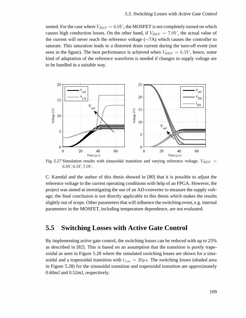
5.5. Switching Losses with Active Gate Control
sented. For the case whereVREF = 6.0V , the MOSFET is not completely turned on whichcauses high conduction losses. On the other hand, ifVREF = 7.0V , the actual value ofthe current will never reach the reference voltage (∼7A) which causes the controller tosaturate. This saturation leads to a distorted drain current during the turn-off event (notseen in the figure). The best performance is achieved whenVREF = 6.5V , hence, somekind of adaptation of the reference waveform is needed if changes in supply voltage areto be handled in a suitable way.
0 20 40 600
5
10
15
20
v
ref
vGS
0 20 40 600
5
10
15
20
25
v
ref
vDS
iDSV
ref
Vref
Volta
ge[V
]
Volta
ge[V
]
Time [µs]Time [µs]
Fig. 5.27Simulation results with sinusoidal transition and varyingreference voltage.VREF =6.0V, 6.5V, 7.0V .
C. Kamdal and the author of this thesis showed in [80] that it is possible to adjust thereference voltage to the current operating conditions withhelp of an FPGA. However, theproject was aimed at investigating the use of an AD-converter to measure the supply volt-age; the final conclusion is not directly applicable to this thesis which makes the resultsslightly out of scope. Other parameters that will influence the switching event, e.g. internalparameters in the MOSFET, including temperature dependence, are not evaluated.
5.5 Switching Losses with Active Gate Control
By implementing active gate control, the switching losses can be reduced with up to 25%as described in [82]. This is based on an assumption that the transition is purely trape-zoidal as seen in Figure 5.28 where the simulated switching losses are shown for a sinu-soidal and a trapezoidal transition withtrise = 20µs. The switching losses (shaded areain Figure 5.28) for the sinusoidal transition and trapezoidal transition are approximately0.60mJ and 0.52mJ, respectively.
109
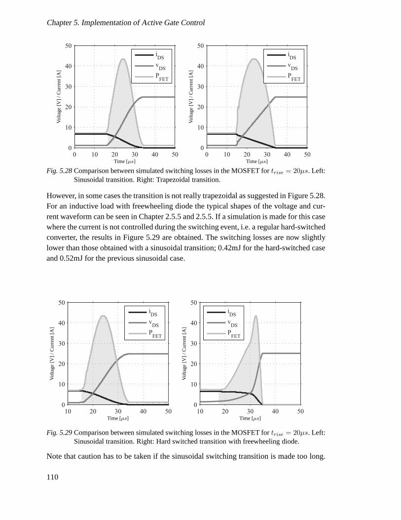
Chapter 5. Implementation of Active Gate Control
0 10 20 30 40 500
10
20
30
40
50
iDS
vDS
PFET
0 10 20 30 40 500
10
20
30
40
50
iDS
vDS
PFET
Volta
ge[V
] /C
urre
nt[A
]
Volta
ge[V
] /C
urre
nt[A
]
Time [µs]Time [µs]
Fig. 5.28Comparison between simulated switching losses in the MOSFET for trise = 20µs. Left:Sinusoidal transition. Right: Trapezoidal transition.
However, in some cases the transition is not really trapezoidal as suggested in Figure 5.28.For an inductive load with freewheeling diode the typical shapes of the voltage and cur-rent waveform can be seen in Chapter 2.5.5 and 2.5.5. If a simulation is made for this casewhere the current is not controlled during the switching event, i.e. a regular hard-switchedconverter, the results in Figure 5.29 are obtained. The switching losses are now slightlylower than those obtained with a sinusoidal transition; 0.42mJ for the hard-switched caseand 0.52mJ for the previous sinusoidal case.
10 20 30 40 500
10
20
30
40
50
iDS
vDS
PFET
10 20 30 40 500
10
20
30
40
50
iDS
vDS
PFET
Volta
ge[V
] /C
urre
nt[A
]
Volta
ge[V
] /C
urre
nt[A
]
Time [µs]Time [µs]
Fig. 5.29Comparison between simulated switching losses in the MOSFET for trise = 20µs. Left:Sinusoidal transition. Right: Hard switched transition with freewheeling diode.
Note that caution has to be taken if the sinusoidal switchingtransition is made too long.
110

5.5. Switching Losses with Active Gate Control
In Figure 5.30 the transition for two different transition times are depicted;trise = 4µs
andtrise = 40µs. For the case where the switching time istrise = 4µs, the energy dis-sipated in the component during one switching event is approximately 0.09mJ and fortrise = 40µs, the energy dissipation is approximately 1.0mJ. From this simulation it canbe concluded that if sinusoidal transitions are to be implemented, the energy dissipationin the component during the switching event has to be thoroughly investigated. For thecurrent switching frequency 2464Hz, the switching losses can be calculated to approxi-mately 4.7W which can be considered relatively high for thistype of application. So, iftrise = 40µs is applied to the component at the current operating case, itis most likely tobreak due to a too high junction temperature. However, underspecial circumstances theremight be an application for this type of switching, e.g. for high voltage DC/DC convertersoperating with IGBT’s where the switching frequency is rather low.
0 2 4 60
10
20
30
40
50
iDS
vDS
PFET
0 20 40 600
10
20
30
40
50
iDS
vDS
PFET
Volta
ge[V
] /C
urre
nt[A
]
Volta
ge[V
] /C
urre
nt[A
]
Time [µs]Time [µs]
Fig. 5.30Comparison between simulated switching losses in the MOSFET. Left: trise = 4µs.Right: trise = 40µs.
111

Chapter 5. Implementation of Active Gate Control
112

Chapter 6
Conclusions
In this thesis a new approach to MOSFET modeling have been presented. The proposedmodel was used to show that it is possible to achieve better controllability of a systemcomprising of varying parameters with an adaptive control algorithm.
Regarding the output of the system, the controllability is significantly better for a systemwhere the drain current is selected as an output compared to asystem where the drain-source voltage is selected as an output. Nevertheless, certain problems are still existingwhere the greatest problem to overcome is how the reference voltage shall be adapted tothe present operating conditions.
The suggested procedure for extracting parameters, although not completely correct froma control theory point of view, gives the possibility to approximate suitable values alreadyat the simulation stage of the development work. It is shown that a single operating pointis not sufficient when the controller parameters are to be determined. The total system isa complex entity with many non-linear variables and a procedure for finding the adaptivecontrol parameters is presented in this thesis.
The principle of active gate control is found to be working sufficiently well for slowerswitching transitions, i.e.> 20µs. For faster transitions, the derived controller structuresstill work, but disturbances can be noticed due to saturation of the controller.
The switching losses can in some cases be lowered if active gate control is applied. Thisstatement holds true for the fastest switching transitions(4µs) investigated in this thesis.
113

Chapter 6. Conclusions
114

Chapter 7
Future Work
Based on the investigations performed in this thesis and theproblems that were encoun-tered, some ideas for further research in this and related fields are outlined below.
• Analyze how the diode capacitance is affected by forward bias. All measurementsin this thesis have been aimed at how the capacitance behaveswhen the diode isreverse biased. One possible scenario might be that the diode capacitance is such asmall contributor to the overall EMI performance; the reverse recovery might be agreater contributor.
• Further analysis of how a correct reverse recovery behaviorcan be modeled. Is theinvestigated model suitable for diodes at this power level?If the investigated modelis found to be suitable, how can the parameters needed for appropriate modeling beextracted?
• Add a diode model with reverse recovery to a system comprising of the proposedMOSFET model and use it as a freewheeling diode when switching an inductiveload. For correct modeling of the EMI performance of the system, correct reverserecovery characteristics needs to be taken into account.
• Use exact linearization to evaluate a more suitable controller circuit. Since themethod for determining controller parameters proposed in this thesis have showncertain deficits, Exact linearization might give better overall performance.
• Digital implementation of pre-charging. This can be done intwo ways; either byimplementing a complete digital control system or by implementing digitally con-trolled potentiometers in the feedback loop of the controller circuit.
• Develop a better algorithm for determining the proportional and integral gain whenadaptive control is used. As previously shown this thesis, the trajectory which thesystem takes during a switching interval is strongly determined by the controller
115

Chapter 7. Future Work
parameters. This gives the need for a very thorough extraction of the parameters thatare suitable for that operating point. Also, it would be of great interest to evaluatewhich quantities that are most suitable for determining thecontroller parameters; inthis thesis wereKp, Ki = f(vGS, vDS), but mightiDS be more suitable?.
• Adaptation of the reference voltage to the current operating conditions. If digitalcontrol is implemented, the reference voltage can adjustedto the current supplyvoltage in order to fully turn on and off the MOSFET without saturating the con-troller.
116
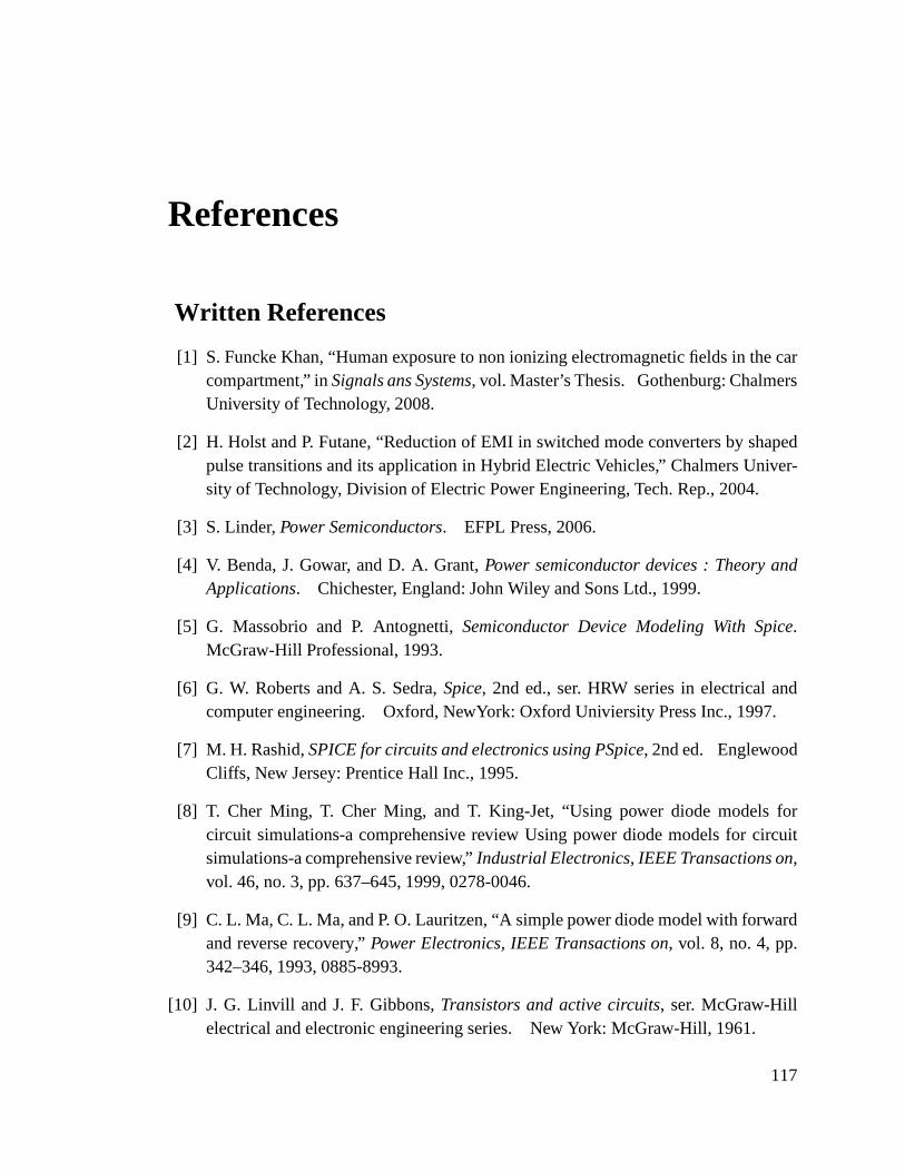
References
Written References
[1] S. Funcke Khan, “Human exposure to non ionizing electromagnetic fields in the carcompartment,” inSignals ans Systems, vol. Master’s Thesis. Gothenburg: ChalmersUniversity of Technology, 2008.
[2] H. Holst and P. Futane, “Reduction of EMI in switched modeconverters by shapedpulse transitions and its application in Hybrid Electric Vehicles,” Chalmers Univer-sity of Technology, Division of Electric Power Engineering, Tech. Rep., 2004.
[3] S. Linder,Power Semiconductors. EFPL Press, 2006.
[4] V. Benda, J. Gowar, and D. A. Grant,Power semiconductor devices : Theory andApplications. Chichester, England: John Wiley and Sons Ltd., 1999.
[5] G. Massobrio and P. Antognetti,Semiconductor Device Modeling With Spice.McGraw-Hill Professional, 1993.
[6] G. W. Roberts and A. S. Sedra,Spice, 2nd ed., ser. HRW series in electrical andcomputer engineering. Oxford, NewYork: Oxford Univiersity Press Inc., 1997.
[7] M. H. Rashid,SPICE for circuits and electronics using PSpice, 2nd ed. EnglewoodCliffs, New Jersey: Prentice Hall Inc., 1995.
[8] T. Cher Ming, T. Cher Ming, and T. King-Jet, “Using power diode models forcircuit simulations-a comprehensive review Using power diode models for circuitsimulations-a comprehensive review,”Industrial Electronics, IEEE Transactions on,vol. 46, no. 3, pp. 637–645, 1999, 0278-0046.
[9] C. L. Ma, C. L. Ma, and P. O. Lauritzen, “A simple power diode model with forwardand reverse recovery,”Power Electronics, IEEE Transactions on, vol. 8, no. 4, pp.342–346, 1993, 0885-8993.
[10] J. G. Linvill and J. F. Gibbons,Transistors and active circuits, ser. McGraw-Hillelectrical and electronic engineering series. New York: McGraw-Hill, 1961.
117

Written References
[11] M. P. Beddoes and M. P. Beddoes, “Linvill’s lumped models and the simplifiedmodel,”Proceedings of the IEEE, vol. 53, no. 5, pp. 552–554, 1965, 0018-9219.
[12] A. Maxim and G. Maxim, “A novel power PIN diode behavioral SPICE macromodelincluding the forward and reverse recoveries and the self-heating process,” vol. 2,2000, pp. 1088–1094 vol.2.
[13] G. M. Buiatti, F. Cappelluti, and G. Ghione, “Power PiN diode model for PSPICEsimulations,” vol. 3, 2005, pp. 1911–1916 Vol. 3.
[14] P. O. Lauritzen, P. O. Lauritzen, and C. L. Ma, “A simple diode model with reverserecovery,”Power Electronics, IEEE Transactions on, vol. 6, no. 2, pp. 188–191,1991, 0885-8993.
[15] C. L. Ma, C. L. Ma, P. O. Lauritzen, and J. Sigg, “Modelingof power diodes withthe lumped-charge modeling technique,”Power Electronics, IEEE Transactions on,vol. 12, no. 3, pp. 398–405, 1997, 0885-8993.
[16] S. Sze and K. K. Ng,Physics of semiconductor devices, 3rd ed. Hoboken, NJ: J.Wiley and Sons, Inc, 2007.
[17] G. Verneau, L. Aubard, J. C. Crebier, C. Schaeffer, and J. L. Schanen, “Empiricalpower MOSFET modeling: practical characterization and simulation implantation,”vol. 4, 2002, pp. 2425–2432 vol.4.
[18] D. P. Foty,MOSFET Modelling with PSpice. Principles and Practice. PrenticeHall, Inc., 1997.
[19] T. M. Undeland, W. P. Robbins, and N. Mohan,Power Electronics : Converters,Applications, and Design. New York : Wiley, cop., 1989.
[20] L. Tihanyi, Electromagnetic Compatibility in Power Electronics. Butterworth-Heinemann, Linacre House, Jordan, Hill, Orford OX2 8DP, United Kingdom, 1995.
[21] “ISOPLUS - The Revolution in Discrete Isolation Technique. Technical ReportIXAN0025. ,” IXYS Semiconductor GmbH, Tech. Rep., 2006.
[22] G. Felic and R. Evans, “Study of heat sink EMI effects in SMPS circuits,” inElec-tromagnetic Compatibility, 2001. EMC. 2001 IEEE International Symposium on,R. Evans, Ed., vol. 1, 2001, pp. 254–259 vol.1.
[23] M. Kchikach, M. H. Pong, and Z. M. Qian, “The influence of magnetic compo-nent on common-mode current in a boost converter,” inPower Electronics and Mo-tion Control Conference, 2000. Proceedings. IPEMC 2000. The Third International,M. H. Pong, Ed., vol. 2, 2000, pp. 925–929 vol.2.
118

Written References
[24] B. Mammano and B. Carsten, “Understanding and Optimizing ElectromagneticCompatibility in Switchmode Power Supplies,”Texas Instrument Inc., 2003.
[25] A. I. Maswood and S. Lim Keng, “Design aspects of planar and conventional SMPStransformer: a cost benefit analysis,”Industrial Electronics, IEEE Transactions on,vol. 50, no. 3, pp. 571–577, 2003, 1557-9948.
[26] C. Rengang, C. Rengang, J. D. van Wyk, S. Wang, and W. G. A.O. W. G. Odendaal,“Planar electromagnetic integration technologies for integrated EMI filters Planarelectromagnetic integration technologies for integratedEMI filters,” in Industry Ap-plications Conference, 2003. 38th IAS Annual Meeting. Conference Record of the,J. D. van Wyk, Ed., vol. 3, 2003, pp. 1582–1588 vol.3.
[27] R. Chen, R. Chen, F. Canales, B. Yang, P. A. B. P. Barbosa,J. D. A. v. W. J. D. vanWyk, and F. C. A. L. F. C. Lee, “Integration of electromagnetic passive componentsin DPS front-end DC/DC converter - a comparative study of different integrationsteps Integration of electromagnetic passive components in DPS front-end DC/DCconverter - a comparative study of different integration steps,” in Applied PowerElectronics Conference and Exposition, 2003. APEC ’03. Eighteenth Annual IEEE,F. Canales, Ed., vol. 2, 2003, pp. 1137–1142 vol.2.
[28] G. A. Kyriazis, “Analysis of discrepancies between measured and predicted con-ducted emissions in switched-mode power supplies,” inElectromagnetic Compati-bility, 1997. IEEE 1997 International Symposium on, 1997, pp. 504–506.
[29] M. Jin, M. Jin, and M. Weiming, “Power Converter EMI Analysis Including IGBTNonlinear Switching Transient Model Power Converter EMI Analysis IncludingIGBT Nonlinear Switching Transient Model,”Industrial Electronics, IEEE Trans-actions on, vol. 53, no. 5, pp. 1577–1583, 2006, 0278-0046.
[30] J. Meng, W. Ma, Q. Pan, L. A. Z. L. Zhang, and Z. A. Z. Z. Zhao, “Multiple SlopeSwitching Waveform Approximation to Improve Conducted EMISpectral Anal-ysis of Power Converters Multiple Slope Switching WaveformApproximation toImprove Conducted EMI Spectral Analysis of Power Converters,” ElectromagneticCompatibility, IEEE Transactions on, vol. 48, no. 4, pp. 742–751, 2006, 0018-9375.
[31] P. R. Mugur, J. Roudet, and J. C. Crebier, “Power electronic converter EMC analysisthrough state variable approach techniques,”Electromagnetic Compatibility, IEEETransactions on, vol. 43, no. 2, pp. 229–238, 2001, 0018-9375.
[32] F. S. Dos Reis, J. C. M. de Lima, V. M. Canalli, and E. F. Magnus, “Conducted EMIsimulation tool,” inPower Electronics Specialists Conference, 2002. pesc 02. 2002IEEE 33rd Annual, vol. 4, 2002, pp. 2033–2038.
119

Written References
[33] G. Ala, G. Ala, M. C. Di Piazza, G. Tine, F. A. V. F. Viola, and G. A. V. G. Vitale,“Evaluation of Radiated EMI in 42-V Vehicle Electrical Systems by FDTD Simula-tion,” Vehicular Technology, IEEE Transactions on, vol. 56, no. 4, pp. 1477–1484,2007, 0018-9545.
[34] R. L. Kirlin, W. Jian, and R. M. Dizaji, “Study on spectral analysis and design forDC/DC conversion using random switching rate PWM,” inStatistical Signal andArray Processing, 2000. Proceedings of the Tenth IEEE Workshop on, 2000, pp.378–382.
[35] Y. Shrivastava, S. Y. Hui, and S. Sathiakumar, “Noise analysis of DC-AC randomPWM schemes,”Power Electronics, IEEE Transactions on, vol. 14, no. 4, pp. 761–770, 1999, 0885-8993.
[36] M. M. Bech, J. K. Pedersen, and F. Blaabjerg, “Field-oriented control of an inductionmotor using random pulsewidth modulation,”Industry Applications, IEEE Transac-tions on, vol. 37, no. 6, pp. 1777–1785, 2001, 0093-9994.
[37] Y. S. Lai, “Sensorless speed vector-controlled induction motor drives using newrandom technique for inverter control,”Energy Conversion, IEEE Transaction on,vol. 14, no. 4, pp. 1147–1155, 1999, 0885-8969.
[38] A. M. Stankovic and H. Lev-Ari, “Randomized modulationin power electronic con-verters,”Proceedings of the IEEE, vol. 90, no. 5, pp. 782–799, 2002, 0018-9219.
[39] A. M. Stankovic, G. E. Verghese, and D. J. Perreault, “Analysis and synthesis ofrandomized modulation schemes for power converters Analysis and synthesis ofrandomized modulation schemes for power converters,”Power Electronics, IEEETransactions on, vol. 10, no. 6, pp. 680–693, 1995, 0885-8993.
[40] T. Tanaka, T. Ninomiya, and K. Harada, “Random-switching control in DC-to-DCconverters,” inPower Electronics Specialists Conference, 1989. PESC ’89 Record.,20th Annual IEEE, 1989, pp. 500–507 vol.1.
[41] T. Tanaka, H. Kameda, and T. Ninomiya, “Noise analysis of DC-to-DC converterwith random-switching control,” inTelecommunications Energy Conference, 1991.INTELEC ’91., 13th International, 1991, pp. 283–290.
[42] Y. Shrivastva, S. Sathiakumar, and S. Y. R. Hui, “Randomdiscrete PWM methodfor DC-DC power converters Random discrete PWM method for DC-DC powerconverters,”Electronics Letters, vol. 32, no. 23, pp. 2105–2106, 1996, 0013-5194.
[43] D. Gonzalez, D. Gonzalez, J. Balcells, A. Santolaria, J. C. A. L. B. J. C. Le Bunetel,J. A. G. J. Gago, D. A. M. D. Magnon, and S. A. B. S. Brehaut, “Conducted EMI Re-duction in Power Converters by Means of Periodic Switching Frequency Modulation
120

Written References
Conducted EMI Reduction in Power Converters by Means of Periodic SwitchingFrequency Modulation,”Power Electronics, IEEE Transactions on, vol. 22, no. 6,pp. 2271–2281, 2007, 0885-8993.
[44] J.-C. Le Bunetel, D. Gonzalez, and J. Balcell, “Impact of Periodic Switching Fre-quency Modulation control to reduce conducted EMI in Power Factor ConvertersImpact of Periodic Switching Frequency Modulation controlto reduce conductedEMI in Power Factor Converters,” inIEEE Industrial Electronics, IECON 2006 -32nd Annual Conference on, D. Gonzalez, Ed., 2006, pp. 2541–2545.
[45] L. Feng, L. Feng, and D. Y. Chen, “Reduction of power supply EMI emissionby switching frequency modulation Reduction of power supply EMI emission byswitching frequency modulation,”Power Electronics, IEEE Transactions on, vol. 9,no. 1, pp. 132–137, 1994, 0885-8993.
[46] K. K. Tse, C. Henry Shu-Hung, S. Y. Ron Hui, and H. C. A. S. H. C. So, “A com-parative study of carrier-frequency modulation techniques for conducted EMI sup-pression in PWM converters A comparative study of carrier-frequency modulationtechniques for conducted EMI suppression in PWM converters,” Industrial Elec-tronics, IEEE Transactions on, vol. 49, no. 3, pp. 618–627, 2002, 0278-0046.
[47] C. R. Paul, Introduction to Electromagnetic Compatibility, 2nd ed. Wiley-Interscience, 2006.
[48] Z. Kai, Z. Yunbin, Z. Yonggao, and A. Y. K. Yong Kang, “Reduction of CommonMode EMI in a Full-Bridge Converter through Automatic Tuning of Gating Signals,”in Power Electronics and Motion Control Conference, 2006. IPEMC ’06. CES/IEEE5th International, Z. Yunbin, Ed., vol. 1, 2006, pp. 1–5.
[49] N. Idir and J. Franchaud, “Gate-Voltage Control Minimizes EMI from IGBTs,”Power Electronics Technology, vol. February, February 2004 2004.
[50] N. Idir, R. Bausiere, and J. J. Franchaud, “Active gate voltage control of turn-on di/dtand turn-off dv/dt in insulated gate transistors,”Power Electronics, IEEE Transac-tions on, vol. 21, no. 4, pp. 849–855, 2006, 0885-8993.
[51] S. Takizawa, S. Igarashi, and K. Kuroki, “A new di/dt control gate drive circuit forIGBTs to reduce EMI noise and switching losses,” inPower Electronics SpecialistsConference, 1998. PESC 98 Record. 29th Annual IEEE, S. Igarashi, Ed., vol. 2,1998, pp. 1443–1449 vol.2.
[52] A. Consoli, S. Musumeci, G. Oriti, and A. A. T. A. Testa, “An innovative EMI reduc-tion design technique in power converters,”Electromagnetic Compatibility, IEEETransactions on, vol. 38, no. 4, pp. 567–575, 1996, 0018-9375.
121

Written References
[53] R. Sachdeva and E. P. Nowicki, “Characterization of a gate drive technique for snub-berless operation of gate controlled devices,” inElectrical and Computer Engineer-ing, 2001. Canadian Conference on, E. P. Nowicki, Ed., vol. 2, 2001, pp. 1085–1089vol.2.
[54] S. Musumeci, A. Raciti, A. Testa, A. Galluzzo, and M. Melito, “Switching-behaviorimprovement of insulated gate-controlled devices Switching-behavior improvementof insulated gate-controlled devices,”Power Electronics, IEEE Transactions on,vol. 12, no. 4, pp. 645–653, 1997, 0885-8993.
[55] J. D. Kagerbauer and T. M. Jahns, “Development of an Active dv/dt Control Al-gorithm for Reducing Inverter Conducted EMI with Minimal Impact on Switch-ing Losses,” inPower Electronics Specialists Conference, 2007. PESC 2007. IEEE,T. M. Jahns, Ed., 2007, pp. 894–900.
[56] A. Kempski, A. Kempski, and R. Smolenski, “Metod of Selection of dv/dt for EMICurrent Ringing Attenuation Metod of Selection of dv/dt forEMI Current RingingAttenuation,” inCompatibility in Power Electronics, 2007. CPE ’07, R. Smolenski,Ed., 2007, pp. 1–5.
[57] A. G. M. Strollo and E. Napoli, “Improved PIN diode circuit model with automaticparameter extraction technique,”Circuits, Devices and Systems, IEE Proceedings -,vol. 144, no. 6, pp. 329–334, 1997, 1350-2409.
[58] H. Chung-Wen, A. Ruehli, and P. Brennan, “The modified nodal approach to net-work analysis,”Circuits and Systems, IEEE Transactions on, vol. 22, no. 6, pp.504–509, 1975, 0098-4094.
[59] L. M. Wedepohl and L. Jackson, “Modified nodal analysis:an essential addition toelectrical circuit theory and analysis,”Engineering Science and Education Journal,vol. 11, no. 3, pp. 84–92, 2002, 0963-7346.
[60] C. Fung-Yue, “The unified nodal approach to circuit analysis,” in Circuits and Sys-tems, 1997. ISCAS ’97., Proceedings of 1997 IEEE International Symposium on,vol. 2, 1997, pp. 849–852 vol.2.
[61] C. Fung-Yuel, “Unified nodal analysis of electronic circuits,” in Circuits and Sys-tems, 1996., IEEE 39th Midwest symposium on, vol. 3, 1996, pp. 1119–1122 vol.3.
[62] C. L. I. M. M L Lucia, J L Hernandez-Rojas, “Capacitance measurements of p-njunctions: depletion layer and diffusion capacitance contributions,”European jour-nal of Physics, no. 14, pp. 86–89, 1993.
[63] M. Pedersen, “A capacitor, a p-n junction, and a MOS circuit - Comparison of differ-ent methods of measurements.” University of Southern Denmark, Tech. Rep., 2002.
122

Written References
[64] “LeCroy Applications Brief No. L.A.B. 418,” Tech. Rep., 2002.
[65] G. Johannesson and N. Fransson, “EMI measurements and modeling of a DC-DCBuck converter,” Chalmers University of Technology, Division of Electric PowerEngineering, Tech. Rep., 2008.
[66] D. Li and P. Mazumder, “Accurate estimating simultaneous switching noises by us-ing application specific device modeling,” inDesign, Automation and Test in EuropeConference and Exhibition, 2002. Proceedings, 2002, pp. 1038–1043.
[67] R. P. Frey, “Advanced Power Technology Aplication NoteAPT0001 - High Voltage,High Efficiency MOSFET RF Amplifiers - Design Procedure and Examples,” Tech.Rep.
[68] K. Xing, F. C. Lee, and D. Boroyevich, “Extraction of parasitics within wire-bondIGBT modules,” inApplied Power Electronics Conference and Exposition, 1998.APEC ’98. Conference Proceedings 1998., Thirteenth Annual, vol. 1, 1998, pp. 497–503 vol.1, [Acessed 2008-10-25].
[69] J. Hammon, S. K. Lam, D. Drury, and M. Ingram, “Compact 1 MV, 10 Hz pulser,”in Pulsed Power Conference, 1997. Digest of Technical Papers.1997 11th IEEEInternational, vol. 1, 1997, pp. 147–152 vol.1.
[70] N. Jurisic and F. Bezanilla, “Letter to the Editor. ,”Journal of Neurophysiology,vol. 96, p. 959, 2006.
[71] K. Kundert,The Designer’s Guide to SPICE and SpectreA R© (The Designer’s GuideBook Series), 1st ed. Springer, 1995.
[72] “Application Note AN-957 - Measuring HEXFET MOSFET Characteristics,” Inter-national Rectifier Inc., Application Note.
[73] Y. Lembeye, J. P. Keradec, and J. L. Schanen, “Experimental characterization of anon linear electrostatic quadripole: application to insulated gate power components,”in Instrumentation and Measurement Technology Conference, 1998. IMTC/98. Con-ference Proceedings. IEEE, vol. 1, 1998, pp. 525–529 vol.1.
[74] Y. Lembeye, J. L. Schanen, and J. P. Keradec, “Experimental characterization of in-sulated gate power components: capacitive aspects,” inIndustry Applications Con-ference, 1997. Thirty-Second IAS Annual Meeting, IAS ’97.,Conference Record ofthe 1997 IEEE, vol. 2, 1997, pp. 983–988 vol.2.
[75] C. Deml, “Input and reverse transfer capacitance measurement of MOS-gated powertransistors under high current flow,” inIndustry Applications Conference, 1999.
123
Internet References
Thirty-Fourth IAS Annual Meeting. Conference Record of the1999 IEEE, vol. 2,1999, pp. 1093–1097 vol.2.
[76] C. Deml and K. Hoffmann, “Gate-drain capacitance behaviour of the DMOS powertransistor under high current flow,” inPower Electronics Specialists Conference,1998. PESC 98 Record. 29th Annual IEEE, vol. 2, 1998, pp. 1716–1719 vol.2.
[77] W. Jie and C. Chen, “Exact linearization of nonlinear differential algebraic systems,”in Info-tech and Info-net, 2001. Proceedings. ICII 2001 - Beijing. 2001 InternationalConferences on, vol. 4, 2001, pp. 284–290 vol.4.
[78] M. Ondera and M. Huba, “Web-based Tools for Exact Linearization Control De-sign,” in Control and Automation, 2006. MED ’06. 14th Mediterranean Conferenceon, 2006, pp. 1–6.
[79] L. Harnefors,Control of Variable-Speed Drives. Vasteras, Sweden: Departmentof Electronics, Malardalens University, 2002.
[80] C. Kamdal, “VHDL Generated Reference Voltage Providing Active Control for aDC/DC Converter,” Department of Space Science, Lulea University of Technology,Sweden, Tech. Rep., 2006.
[81] B. Lennartsson,Reglerteknikens grunder. Lund, Sweden: Studentlitteratur, 2002.
[82] A. Karvonen, H. Holst, T. Tuveson, T. Thiringer, and P. Futane, “Reduction of EMIin Switched Mode Converters by Shaped Pulse Transitions,” in SAE World Confer-ence 2007. Detroit, Michigan, USA: SAE International, 2007.
[83] J. Kaewchai, W. Khangern, and S. Nitta, “Controlling conducted EMI emission ona Buck-boost converter using gate controlled circuit,” inElectromagnetic Compati-bility, 2002 3rd International Symposium on, W. Khangern, Ed., 2002, pp. 541–544.
Internet References
[84] S. Malouyans, “Application Note 975B - SPICE Computer Models for HEXFETPower MOSFETs,” International Rectifier Inc., ApplicationNote, [Accessed 2006-10-27].
[85] P. Turkes, M. Marz, and P. Nance, “Application Note AN-PSM1e - Spicemodels for SIPMOS components,” 2001, [Accessed 2007-03-10]. Available:http://www.infineon.com/upload/Document/anpsm1e.pdf
124

Internet References
[86] “Power Spice Model User Manual, Version 1.5,”13, March 2006 1996, [Accessed 2007-01-17]. Available:http://www.fairchildsemi.com/modelsstatic/spicemanual.html
[87] “International Rectifier IRF520N HEXFET Power MOSFET Datasheet,PD - 91339A,” 1998, [Accessed 2009-01-27]. Available:http://www.irf.com/product-info/datasheets/data/irf520n.pdf
[88] K. Kundert, “Modeling Varactors,” 2006, [Accessed 2008-10-25].
[89] C. Basset and B. Hirasuna, “A Nonlinear Capacitor Modelfor Use in PSpice,” 1999, [Accessed 2008-10-25]. Available:www.cadence.com/appnotes/ANonlinearCapacitorModelForUseInPSpice.pdf
125

Internet References
126

Appendix A
Symbols and Glossary
Symbols
Cchannel Gate-oxide capacitance in the channel region for the power MOS-FET (F)
Cd Diffusion capacitance (F)CD Total pn-junction capacitance (F)Cdepletion Depletion capacitance in the channel region for the power MOS-
FET (F)CDS Drain-source capacitance (F)Cfield−oxide Field-oxide capacitance in the power MOSFET (F)CGD Gate-drain capacitance (F)CGS Gate-source capacitance (F)Cj Depletion capacitance (F)Cj(0) Zero bias capacitance (F)Cox Gate-oxide capacitance in MOSFET modeling (F)Cpp Parallel plate capacitance for the MOS interface in a power MOS-
FET (F)Dn Diffusion coefficient for electrons (cm2s−1)εs Dielectric permittivity of silicon (F/cm)iF Forward current in a diode (A)IS Saturation current (A)k Boltzmann constant (J/K)ki Integral gain for a controllerkp Proportional gain for a controllerλ Channel length modulation parameter
127

Ln Diffusion length for electrons (cm)Leff Effective channel length (cm)µ Carrier Mobility (cm2V−1s−1)NA acceptor concentration (cm−3)ND acceptor concentration (cm−3)Racc Accumulation resistance in the power MOSFETΩRchannel Channel resistance in the power MOSFETΩRdrift Resistance in the drift region for the power MOSFETΩRDS(on) On-state resistance for the power MOSFETΩRG External gate-resistanceΩRJFET JFET-effect resistance in the power MOSFETΩRn n-source contact resistance in the power MOSFETΩτn Carrier Lifetime for electrons (s)τ Time constant for diode modeling proposed by Lauritzen(s)T Temperature (K)Tm Transit time across the intrinsic region for diode modelingpro-
posed by Lauritzen(s)Vbi Built-in voltage for pn-junction (V )VDS Drain-source voltage (V )VGD Gate-drain voltage (V )VGS Gate-source voltage (V )VGS(on) Gate-source voltage, final value (V )Vt Thermal voltage (V )Vth Threshold voltage (V )Wi Width of intrinsic region (m)Weff Effective channel width (cm)q Elementary charge (C)qE Charge located close to the semiconductor junctions, for diode
modeling proposed by Lauritzen (C)qM Charge located in the intrinsic region, for diode modeling pro-
posed by Lauritzen (C)QD Total charge in a pn-junction (C)Qj Depletion charge (C)Qd Diffusion charge (C)
128

AbbreviationsBJT Bipolar Junction TransistorCISPR Special International Committee on Radio Interference
(Eng)Comite International Special des Perturbations Ra-dioelectriques (Fr)
DUT Device Under TestEMC Electromagnetic CompatibilityEMI Electromagnetic InterferenceFDTD Finite Difference Time DomainFPGA Field Programmable Gate ArrayIEC International Electrotechnical CommissionIGBT Insulated Gate Bipolar TransistorJFET Junction gate field-effect transistorIMC Internal Model ControlMNA Modified Nodal AnalysisMOSFET Metal Oxide Field Effect TransistorPiN pn-diode with intrinsic regionPEEC Partial Element Equivalent CircuitPWM Pulse Width ModulationPPM Pulse Position ModulationSMPS Switch Mode Power SupplySPICE Simulation Program with Integrated Circuit EmphasisUNA Unified Nodal AnalysisVDMOS Vertically diffused double MOSFET
129

130

Appendix B
Derivations of Essential Formulas
Derivation of the Threshold Voltage
If a metal-oxide-semiconductor interface with a positive bias voltage is considered, thethreshold of strong inversion in terms of the potential differenceVs in silicon. The holeconcentration in a non-depleted silicon material can be written as
p = NA = ni · exp
(
Ei − EF
kT
)
(B.1)
If Equation (B.1) is rearranged, the difference in energy betweenEF andEi can be writtenas
∆E1 = Ei − EF = kT · ln(
NA
Ni
)
(B.2)
To be able to analyze the energy condition at the occurrence of inversion, it is necessaryto increase the gate-body potential so much that the Fermi energy at the silicon/oxideinterface crosses the intrinsic energy level. If this happens, the electron concentration willexceed the hole concentration. Even though the channel region originally is ap-dopedregion, electrons will now be the majority carrier. This state is referred to asinversionwhich in turn can be divided into two separate characterizations. The first is the so calledweak inversionand is characterized by an electron concentration that still is much lowerthan the acceptor concentration (NA). If the energy levels are considered, the criteria forweak inversion can be written as
(EF − Ei) |Surface< (Ei − EF ) |Body (B.3)
Under these conditions, the electron concentration (n) is still much lower than the acceptorconcentration (NA) which gives no significant change in the space-charge concentrationand consequently the electric field and potential.
131

As the gate potential is increased even further, the electron concentration (ns) at the sil-icon/oxide interface is successfully increased. When the electron concentration reachesthe concentration of acceptors the energy levels can be expressed as
(EF − Ei) |Surface= (Ei − EF ) |Body (B.4)
The interface is now in strong inversion which is characterized by the fact thatns = NA.
The hole concentration in the non-depleted region as a function of the Fermi level can beexpressed as
p = NA = ni · exp
(
Ei − EF
kT
)
(B.5)
From Equation (B.5) the energy difference can be expressed as
∆E = Ei − EF = kt · ln(
NA
Ni
)
(B.6)
If (B.4) is inserted in (B.6) the required energy to reach thebeginning of strong inversioncan be expressed as
∆Etot = 2 · ∆E = 2kt · ln(
NA
Ni
)
(B.7)
The potential difference can be calculated by dividing the energy difference by the elec-tron charge,q, according to
VS |strong inversion=2kT
q· ln
(
NA
Ni
)
(B.8)
whereVS is the potential drop in the silicon from the silicon-oxide interface to the bodycontact. In the strongly inverted region, the electron concentration depends exponentiallyon the position of the Fermi level. Hence, as the gate-body potential increases even further,all of the additional charge is built up in the region of the strong inversion. The depletionlayer has reached its maximum. If considering Poissons equation, the change inE-fieldcan be expressed as
dE
dx= −qNA
εSi
(B.9)
If integrated, the distribution of theE-field can be expressed as
E(x) = Emax − x · qNA
εSi
(B.10)
If the entire space charge region is integrated as
132

VS =qNA
2εSi
· W 2 (B.11)
By comparing Equations (B.11) and (B.8), the maximum thickness of the depletion layerat the edge of strong inversion can be expressed as
2kT
q· ln
(
NA
Ni
)
=qNA
2εSi
· W 2 ⇒ Wmax =
√
4εSikT · lnNA
ni
q2NA
(B.12)
The minimum gate-body voltage needed for strong inversion to occur is known as thethreshold voltage, which equals to the sum of the voltage drop in the silicon andin theoxide area. The stored charge at the metal/oxide interface,Qm, must be exactly the sameas the stored charge as in the silicon region,QSi, but with inverse sign.
QSi = −qNAWmax (B.13)
Poissons equation gives the electric field strength in the oxide layer as
Eox =Qm
εox
(B.14)
By assuming that the oxide is free of space-charge, i.e. the electric field strength in theoxide is constant, the voltage drop in the oxide can be expressed as
∆Vox = εox · tox =Qm
εox
· tox =Qm
εox
· tox =qNAWmax
εox
tox (B.15)
The threshold voltage can now be written as
VT = ∆Vox + VS |strong inversion=qNAWmax
εox
· tox +2kT
q· ln
(
NA
ni
)
(B.16)
Equation (B.12) inserted in (B.15) gives an expression for the threshold:
Vth =
√
4NAεSikT · ln(
NA
Ni
)
εox
· tox + 2kT
q· ln
(
NA
Ni
)
(B.17)
As a final step, the gate-oxide capacitance per unit area can be expressed as
Cox =εox
tox
(B.18)
wheretox is the gate oxide thickness expressed in [m]. If B.18 is inserted in B.17, the finalresults yields a commonly used formula for the threshold voltage:
Vth =
√
4NAεSikT · ln(
NA
Ni
)
Cox
+ 2kT
q· ln
(
NA
Ni
)
(B.19)
133

Drain Current for the MOSFET in the Ohmic Region
Assuming a MOSFET that ha reached the state of strong inversion, the current-voltagecharacteristics can be derived. If a field of strong inversion is considered, the currentthrough this field is strongly dependent on the electric field, consists only of majoritycarriers and can be expressed as
Jdrift = (qµnn + qµpp)E −→ Je = µeQinv
dV (x)
dx(B.20)
whereµ is the carrier mobility,Qinv is the total electron charge in the channel region andVGS is the applied gate-body potential. Once the threshold voltage is reached, almost allexcess charge is built up in the channel region, the MOSFET then exhibits the propertiesof a parallel plate capacitor. The inversion layer charge can be assumed to be proportionalto the applied voltage. Also, at and below the threshold voltage, the inversion layer chargeis zero. Hence, the inversion charge can be described by
Qinv = Cox(VGS − Vth) (B.21)
whereQinv is the charge in the inversion channel of the semiconductingmaterial,Cox isthe parallel plate gate-oxide capacitance,VGS is the applied gate-body voltage andVth
is the threshold voltage derived in Appendix B. The charge can also be described as afunction of the potential at the silicon-oxide interface with respect to the source as
Qinv(x) = Cox(VGS − Vth − V (x)) (B.22)
whereV (x) is the potential along the channel region.
If B.22 is inserted in B.20, the following expression for thedrain current density is ob-tained
Je = −µeCox(VGS − Vth − V (x))dV (x)
dx(B.23)
Rearrange and separate the variables according to
Jedx = −µeCox(VGS − Vth − V (x))dV (B.24)
Integrate over the entire channel length whereV = 0 aty = 0 andV = VDS aty = L.
LChannel∫
0
Jedy =
VDS∫
0
−µeCox(VGS − Vth − V (x))dV (B.25)
Solving gives
134

Je =−µeCox
L
(
VGS − 1
2VDS − Vth
)
VDS (B.26)
The total current can be written as
ID = −JeW (B.27)
which gives the final expression for the drain current
ID = µeCox
W
L
(
VGS − 1
2VDS − Vth
)
VDS (B.28)
This equation is valid for the drain current as long as stronginversion prevails in all pointsof the channel, i.e. as long as the channel is not pinched off.Equation (B.28 is only valid aslong as(VDS < (VGS − Vth), the MOSFET is operating in the linear region.VGS controlsthe electron concentration in the channel andVDS controls the lateral electric field in thechannel.
Drain Current for the MOSFET in the Active Region
According to the derivation in Appendix B, the equation for the drain current is only validin the linear region. AsVDS reaches or exceedsVGS − Vth the electron concentration atx = L drops to very small concentrations, only a depletion regionis existing and thechannel is said to be pinched off. All additional applied drain-source voltage is consumedby the depletion region, hence isID independent ofVDS
IDsat = ID (VDS = VGS − Vth) (B.29)
which gives a drain current that can be expressed as
IDsat = µeCox
W
2L(VGS − Vth)
2 (B.30)
In the saturation regime,ID is modulated byVGS but independent ofVDS. VGS controlsboth the electron concentration in the channel and the lateral electric field in the channel.VDS does not affect the lateral field in the channel due to pinch-off.
135

136

Appendix C
Selected Publications
Paper I
J. Paixao, A. Karvonen, J.Astrom, T. Tuveson, and T. Thiringer, ”EMI Reduc-tion Using Symmetrical Switching and Capacitor Control” published at2008Asia-Pacific Symposium on Electromagnetic Compatibility in conjunction withthe 19th Intern. Zurich Symposium on Electromagnetic Compatibility , Singa-pore, 2008.
137

138

EMI Reduction Using Symmetrical Switching and Capacitor Control
Julia Paixão#1, Andreas Karvonen#2, Johan Åström#3, Trygve Tuveson*4, Torbjörn Thiringer#5 #Division of Electric Power Engineering
Department of Energy and Environment
Chalmers University of Technology
Hörsalsvägen 11, SE-412 96, Gothenburg, Sweden [email protected]
*EMC Services Elmiljöteknik AB
Mölndal, Sweden [email protected]
Abstract— An EMI reduction technique using two MOSFETs
instead of a single MOSFET in a step-down converter is
investigated in this article. A circuit that implements this
technique together with external capacitor control was designed
and measurement results were compared against simulations.
The switching element in the proposed circuit is an IRF7309 that
consists of a p-channel and an n-channel MOSFET in the same
package. The entire circuit also consists of an input circuit for
the control pulses and a controller circuit responsible for
optimizing the turn-on and turn-off of the p-channel MOSFET
and n-channel MOSFET. The effect of difference in the threshold
voltage between the two MOSFETs is controlled by external
capacitances in a configuration referred to as capacitor control.
The analyzes of simulations and measurement results show that
the symmetrical switching (or double MOSFET switching)
technique can successfully be applied to reduce the RF emission
in the low frequency and medium frequency range when
compared to the single MOSFET switching.
I. INTRODUCTION
Following the increased number of power electronic converters in many applications, such as houses, vehicles, etc, the concern for electromagnetic interference (EMI) is increasing. If electrical equipment unintentionally generates electromagnetic interference in the RF range, there is a substantial risk that it will interfere with other equipment such as radio receivers. One particular situation of an unintended RF interference source is when a single switch buck converter is located far from the load, for instance light bulb control in a vehicle. In this situation, the wires between the converter and the load act as an antenna radiating electromagnetic waves due to the variation of the electric field. Traditionally, the most popular method of EMI mitigation is passive filtering techniques which often are implemented late in the project phase at a significant size and cost penalty. As an alternative to passive filtering for common mode conducted EMI mitigation, a new circuit topology is presented in this article that actively cancels the common mode voltage created by the
converter. The single switching signal is transformed into two signals that are symmetrical to each other and hereby cancel out the antenna effect by eliminating the resulting variations in the electric field. This can be accomplished by utilizing two switching elements in a configuration called Double MOSFET Switching (or Symmetrical Switching) instead of one element as used in a regular step-down converter. According to Erkuan and Lipo [1], the common mode noise in electrical applications such as AC-machine inverters can fail conducted EMI tests even before power to the load is applied due to EMI generated by the internal power supplies. For this reason, to meet today's stringent specifications, attention must be given to any sub-system that would contribute to the overall EMI production.
The authors have identified one reference [2] that apply a similar technique to a DC-DC buck converter. Here, an active cancellation of common mode (CM) voltage is applied to a simple buck converter by using double MOSFET switching. However, the main purpose in the previous article was to create a stable power supply for an inverter drive. Further on, the concept of double MOSFET switching has been applied to three phase and six phase inverters [3][4]. In the prolongation, this technique can be used in many power electronic topologies such as a step down-converter discussed in this article. The main area of application for the step-down converter proposed in this article is automotive applications where the load is located far from the switching unit and is fed with long unshielded wires.
The overall purpose of the article is to investigate and implement the symmetrical switching principle. Moreover, based on the work performed in [5], further improvements such as an improved circuit layout and control stage are implemented and investigated. Further on, the structure and influence of the error handling circuit is investigated.
The following sections will in detail explain the idea behind symmetrical switching and how to implement it. The design of

each part of the circuit will be described in detail together with a brief explanation of the implementation of the complete circuit. The most important SPICE simulations and circuit measurements, as well as the comparison between them, will be presented in the section about the results. Finally, a comparison between double MOSFET switching and single MOSFET switching regarding the reduction of emissions will be done and final conclusions will be drawn.
II. DOUBLE MOSFET SWITCHING IDEA
A. Cancellation Technique
In order to reduce RF-emissions from the wires between the switching equipment and the load, a cancellation technique that operates by splitting the switching voltage into two paths with 180º phase difference and equal magnitude is proposed. The split signal is intended to cancel out the variation in the electric field and consequently, reduce the electromagnetic emission.
B. Proposed Setup
In this article, the cancellation technique is achieved by using two controlled switching devices which are switching symmetrically against each other. This can be compared with a regular converter that utilizes only one single switching device to drive the load. The chosen switching device in the proposed converter is a MOSFET due to the widespread use in low to medium power switching DC/DC supplies.
Rload
VUPPER
VLOWER
InputPMOS
InputNMOS
PMOS
NMOS
VBAT
RGATE
RGATE
10kΩ
10kΩ
Fig. 1. MOSFET setup for symmetrical switching
An overview picture of the proposed setup is shown in Fig. 1 where the switching devices and the load are depicted. The working principle is as follows; the upper MOSFET produces the upper voltage VUPPER while the lower MOSFET produces the lower voltage VLOWER. When the upper and lower MOSFETs are conducting, VUPPER and VLOWER are respectively VBAT and zero, and the voltage over the load is VBAT. When the upper and lower MOSFETs are in off-state, VUPPER and VLOWER are approximately VBAT/2 which results in a voltage over the load that equals to zero.
When double switching is used, the voltage over the load switches between zero and VBAT, similarly to single switching.
The most important difference between double and single switching is that, in the double switching, the sum of VUPPER and VLOWER equals VBAT at all times. Consequently for an ideal converter with double switching, a DC-signal is seen from the external interface which gives a reduction in the common mode voltage and also the high frequency disturbances originating from the cables supplying the load.
III. CIRCUIT DESIGN
As the sum of VUPPER and VLOWER should be equal to VBAT at all times, it is essential that VUPPER and VLOWER are as symmetrical as possible. Such a difference will occur due to the difference in electron mobility between n-doped and p-doped silicon which results in different switching characteristics for an n-channel MOSFET and a p-channel MOSFET. Also, an n-channel device will show a lower on-state resistance if compared with a p-channel device with identical geometry for the same reason [6]. The proposed solution is to compensate the difference of time constants between the p-channel and the n-channel device by using polarized gate resistors with different values for each MOSFET. The polarization utilizes one value of gate resistance for the turn-on and a different value of gate resistance for the turn-off for each MOSFET. By doing this, the maximum turn-on and turn-off time constants can be approximated for both the PMOS and NMOS. However, even though the gate resistors are optimized, the temperature dependence of the parameters can introduce a small error. One way to implement an error handling circuit is to define one MOSFET as a master and the other as a slave. The MOSFET that acts as a slave will have the switching signal added with a regulated feedback signal from the load as its input. The block diagram in Fig. 2 shows the setup of the converter.
PowerSupply
InputCircuit Controller
Circuit
ErrorhandlingCircuit
CapacitorControl
MOSFET
Fig. 2. Block diagram over the proposed converter setup.
The complete converter, including error handling system and polarized gate resistors, was implemented on a PCB where the load is externally connected to the board via two unshielded wires. Due to its experimental nature, the converter uses an external reference square wave generator.
IV. REGULATOR DESIGN
As described in previous section, the proposed way to handle the switching error between the MOSFETS is to define one MOSFET as a master and the other MOSFET as a slave. The MOSFET that acts as a slave will use the previously designed input signal added with a regulated signal from the

load as its input. For the selected MOSFET IRF7309, the PMOS device has larger CGD capacitance than the NMOS and due to the design of the proposed converter; it also has a more complicated input stage that adds a propagation delay. These characteristics makes the dynamics of the PMOS slower than the NMOS, and for that reason, the PMOS is defined as the master MOSFET.
In order to implement an error handling circuit with sufficiently high bandwidth, the regulator must be carefully chosen. The main regulator structure analyzed in this article is a P-regulator realized by the operational amplifier LM6144ANS. For the P-regulator which also is used as a non inverting summer, the error voltage can be expressed as
+
+
+=
LOWER
LOWER
UPPER
UPPER
LOWERUPPER
fs
errorR
V
R
V
RR
RRV
11
1 (1)
where Verror is the error voltage detected by the controller
circuit, Rs is the resistor connected from the inverting input to ground, Rf is the feed forward resistor and VUPPER, RUPPER, VLOWER and RLOWER are the PMOS and NMOS voltage respectively with belonging series resistors. If the error, E, is defined as E = VBAT-(VUPPER+VLOWER). The final error signal can be described as
21
2
1 BAT
s
f
error
V
R
REV +
+−= (2)
where Verror is the same error voltage as in Eq. 1. This
corresponds to the relation that describes the P regulator, but with a voltage offset of VBAT/2.
The regulator output is then added to the NMOS input signal via an operation amplifier used as a non-inverting summer. The resulting signal is then fed to the gate of the NMOS. Note that depending on the results from the previously described summation, the regulator output must be able to produce negative voltage. This causes a need to supply the second operational amplifier stage with a negative voltage source; in this case it is achieved by an additional voltage converter that delivers -10V. The chosen converter is the Maxim MAX680.
V. SIMULATION AND MEASUREMENT RESULTS
The simulations of the circuit were made in OrCad Capture that uses PSpice which is an industry standard circuit simulation language. The implemented circuit uses the parameters specified in Table 1.
TABLE 1 COMPONENT PARAMETERS FOR SIMULATIONS
Quantity Value Quantity Value
VREF 12V RG,ON 1.6kΩ (NMOS) fREF 2.5kHz RG,OFF 1.7kΩ (NMOS) VBAT 12V RG,ON 1kΩ (PMOS)
Rf 10.3kΩ RG,OFF 1kΩ (PMOS) Rs 10.0kΩ RLOAD 6.58Ω
The most important observation from the comparison
between simulations and measurements is that the measured
switching waveforms show a slightly different threshold
voltage compared with the simulation results. These
oscillations most likely originate from the discrepancy in
switching behaviour between the MOSFET SPICE model and
the real device. It is well known that the classical SPICE
MOSFET Model has certain deficits when it comes switching
behaviour which is e.g. described in [7] among others.
0 50 100 150 200 250 300 350 400
-2
0
2
4
6
8
10
12
14
Time (us)
Voltage (V
) / Current(A)
VGD(PMOS)
VGS(NMOS)
Iload
VBAT
Fig. 3. Comparison between simulations and measurements for double
MOSFET switching with regulator and polarized resistance set-up –
VGD P-MOS, VGS N-MOS, Iload and VBAT (supply voltage to the load).
0 50 100 150 200 250 300 350 400
-2
0
2
4
6
8
10
12
14
Time (us)
Voltage (V
) / Current(A)
VD(PMOS)
VD(NMOS)
Iload
VBAT
Fig. 4. Comparison between simulations and measurements for double
MOSFET switching with regulator and polarized resistance set-up –
VDS P-MOS, VDS N-MOS, Iload and VBAT (supply voltage to the load).
In Fig. 3 and Fig. 4, the simulation and measurement results
are compared to each other where continuous lines represent
measurement results and dotted lines represent simulation
results. As seen, the results correspond well to each other.
In order to verify the expected frequency content of the
radiated emissions in the wires when comparing double
MOSFET switching and single MOSFET switching, the FFT
of the sum of VUPPER and VLOWER for the measured and
simulated configuration were calculated using MATLAB. Fig.
5 and Fig. 6 show the magnitude of the FFT components
expressed in dBV. As expected, the double MOSFET
switching shows a lower voltage component in the frequency
range from 1 kHz up to 0.3 MHz compared to single
MOSFET switching. This is an indication that the double
MOSFET switching is a viable alternative to reduce radiated
emissions on wires between a DC/DC converter and the load
when they are located at a large distance from each other.
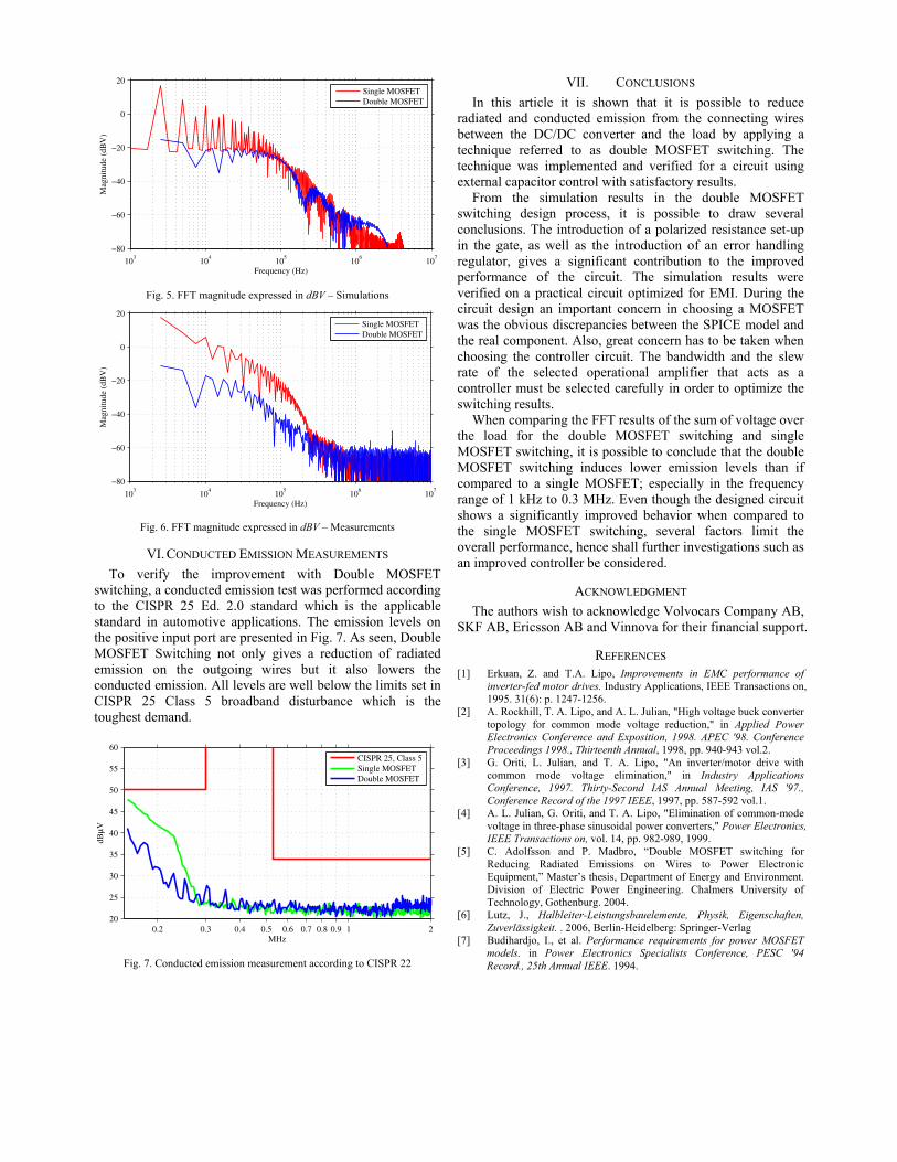
103
104
105
106
107
−80
−60
−40
−20
0
20
Frequency (Hz)
Mag
nit
ude
(dB
V)
Single MOSFET
Double MOSFET
Fig. 5. FFT magnitude expressed in dBV – Simulations
103
104
105
106
107
−80
−60
−40
−20
0
20
Frequency (Hz)
Mag
nit
ude
(dB
V)
Single MOSFET
Double MOSFET
Fig. 6. FFT magnitude expressed in dBV – Measurements
VI. CONDUCTED EMISSION MEASUREMENTS
To verify the improvement with Double MOSFET
switching, a conducted emission test was performed according
to the CISPR 25 Ed. 2.0 standard which is the applicable
standard in automotive applications. The emission levels on
the positive input port are presented in Fig. 7. As seen, Double
MOSFET Switching not only gives a reduction of radiated
emission on the outgoing wires but it also lowers the
conducted emission. All levels are well below the limits set in
CISPR 25 Class 5 broadband disturbance which is the
toughest demand.
0.2 0.3 0.4 0.5 0.6 0.7 0.8 0.9 1 2
20
25
30
35
40
45
50
55
60
MHz
dB
µV
CISPR 25, Class 5
Single MOSFET
Double MOSFET
Fig. 7. Conducted emission measurement according to CISPR 22
VII. CONCLUSIONS
In this article it is shown that it is possible to reduce
radiated and conducted emission from the connecting wires
between the DC/DC converter and the load by applying a
technique referred to as double MOSFET switching. The
technique was implemented and verified for a circuit using
external capacitor control with satisfactory results.
From the simulation results in the double MOSFET
switching design process, it is possible to draw several
conclusions. The introduction of a polarized resistance set-up
in the gate, as well as the introduction of an error handling
regulator, gives a significant contribution to the improved
performance of the circuit. The simulation results were
verified on a practical circuit optimized for EMI. During the
circuit design an important concern in choosing a MOSFET
was the obvious discrepancies between the SPICE model and
the real component. Also, great concern has to be taken when
choosing the controller circuit. The bandwidth and the slew
rate of the selected operational amplifier that acts as a
controller must be selected carefully in order to optimize the
switching results.
When comparing the FFT results of the sum of voltage over
the load for the double MOSFET switching and single
MOSFET switching, it is possible to conclude that the double
MOSFET switching induces lower emission levels than if
compared to a single MOSFET; especially in the frequency
range of 1 kHz to 0.3 MHz. Even though the designed circuit
shows a significantly improved behavior when compared to
the single MOSFET switching, several factors limit the
overall performance, hence shall further investigations such as
an improved controller be considered.
ACKNOWLEDGMENT
The authors wish to acknowledge Volvocars Company AB,
SKF AB, Ericsson AB and Vinnova for their financial support.
REFERENCES
[1] Erkuan, Z. and T.A. Lipo, Improvements in EMC performance of
inverter-fed motor drives. Industry Applications, IEEE Transactions on,
1995. 31(6): p. 1247-1256.
[2] A. Rockhill, T. A. Lipo, and A. L. Julian, "High voltage buck converter
topology for common mode voltage reduction," in Applied Power
Electronics Conference and Exposition, 1998. APEC '98. Conference
Proceedings 1998., Thirteenth Annual, 1998, pp. 940-943 vol.2.
[3] G. Oriti, L. Julian, and T. A. Lipo, "An inverter/motor drive with
common mode voltage elimination," in Industry Applications
Conference, 1997. Thirty-Second IAS Annual Meeting, IAS '97.,
Conference Record of the 1997 IEEE, 1997, pp. 587-592 vol.1.
[4] A. L. Julian, G. Oriti, and T. A. Lipo, "Elimination of common-mode
voltage in three-phase sinusoidal power converters," Power Electronics,
IEEE Transactions on, vol. 14, pp. 982-989, 1999.
[5] C. Adolfsson and P. Madbro, “Double MOSFET switching for
Reducing Radiated Emissions on Wires to Power Electronic
Equipment,” Master’s thesis, Department of Energy and Environment.
Division of Electric Power Engineering. Chalmers University of
Technology, Gothenburg. 2004.
[6] Lutz, J., Halbleiter-Leistungsbauelemente, Physik, Eigenschaften,
Zuverlässigkeit. . 2006, Berlin-Heidelberg: Springer-Verlag
[7] Budihardjo, I., et al. Performance requirements for power MOSFET
models. in Power Electronics Specialists Conference, PESC '94
Record., 25th Annual IEEE. 1994.

Paper II
A. Karvonen, H. Holst, T. Tuveson, T. Thiringer, and P. Futane, ”Reduction ofEMI in Switched Mode Converters by Shaped Pulse Transitions” published atSAE World Conference 2007. Detroit, Michigan, USA. Copyright SAE Interna-tional, 2007.
The work is here reproduced in print with kind permission from the publisher.
Copyright c© SAE International 2007
143

1
Reduction of EMI in Switched Mode Converters byShaped Pulse Transitions
Andreas Karvonen, Henrik Holst, Tryggve Tuveson, Torbjorn Thiringer, and Pravin Futane
Abstract— An idea of reducing the amplitude of higher orderharmonic frequencies from PWM switching pattern is presentedand analyzed in this paper. For experimental studies a flexi-ble curve shaping circuit was developed and implemented forachieving and controlling smooth transitions in a DC/DC PWMcontrolled converter for a 12 V system. A comparison betweentrapezoidal and sinusoidal transitions is made and it is found thata sinusoidal transition gives better EMI performance withoutincreasing the switching losses. In order to further reducetheEMI, a strategy of controlling the output voltage transitions in aMOSFET by ”pre-charging” its gate is derived and investigated.
The developed practical circuit is tested with sinusoidal refer-ence for a purely resistive load and an R-L load. Frequencyresponses obtained from simulations and measurements arecompared and discussed.
Index Terms— EMC, EMI, DC/DC, PWM converter
I. I NTRODUCTION
ELECTROMAGNETIC compatibility, EMC, is an impor-tant consideration for development of electrical circuits,
especially in the field of power electronics. It is not unusualthat circuits are designed for their desired functionalityandafter that any occurring EMI problems are solved by modify-ing the circuit, shielding of the circuit, twisting of connectedcables, using EMI filter etc. Many times this approach endsup in costly, time consuming, trial and error solutions. Forautomotive applications the EMI concern is becoming morecritical since the trend is that mechanically operated objects(actuators, loads, etc) are being replaced by electronicallycontrolled ones. These electrical loads often demands variablepower at a varying voltage level, hence DC/DC convertersare employed more and more. Examples of applications usingswitching power supplies in vehicles are: fuel pump, seatheaters, rear window heaters, beam lights etc.
By attacking the EMI noise generation at the source itself,during the initial design of the circuit, a redesigning processdue to EMI noise problems can be avoided. In addition, if EMIis reduced by this method the bulkiness of possible EMI filterand other radiation-limiting measures can also be reduced.
In the literature there are several design techniques pre-sented which deals with reduction of EMI from switchingpower electronic applications. One method is to use a Ran-domized Pulse Width Modulation (RPWM) [1], [2]. Thistechnique does not actually reduce the EMI noise, instead it
This work was supported by Vinnova, Volvo Car Corporation, SaabMicrowave systems, Ericsson AB and SKF Automotive Division.
Henrik Holst, are with Condesign Electro Guide in collaboration with VolvoCar Company, Andreas Karvonen, Pravin Futane and TorbjornThiringer arewith Chalmers University of Technology, Goteborg and Tryggve Tuvesson, iswith Volvo Car Corporation, Goteborg.
distributes the noise into a wider frequency region. Anotheroption is to use soft switching circuits like resonant converters[4]. Because of their complexity in control and difficultiesin obtaining dynamic performance they have not becomecommon in industrial applications [3].
[8] presents a strategy of reducing the current or voltagerate-of-rise by applying intermediate voltage levels on thegate control voltage of isolated gate transistors placed inabuck converter configuration. The strategy is compared withthe method of increasing the gate resistance [5], [6] and [7].The result showed that the EMI performance was similar forthe two configurations while the switching power losses werelower for the configuration with intermediate voltage levels.
In [5], [6] and [7] control of the drain currentdi/dt in aswitching power MOSFET was obtained by tuning the gateresistance. A reduction indi/dt also leads to a reduction indv/dt and accordingly to a reduction in the produced EMInoise. In [9] an EMI supression driver circuit is presentedwhich directly acts ondv/dt instead. The proposed circuitsenses thedVdrain/dt during turn off, and selectively adjuststhe VGS transition time at a voltage near the threshold volt-age. By this techniquedVdrain/dt is reduced and hence theproduced EMI noise and switching power losses is kept at aminimum.
The purpose of this paper is to evaluate a strategy to reducethe EMI noise by controllingdv/dt of the drain to sourcevoltage during switching of a MOSFET located in a buckconverter for a 12 V system. The idea is to makeVDS toresemble a sinusoidal curve during the switching. In this waya smooth transition of the output voltage is obtained. Theresulting EMI noise using this method is then to be comparedwith the case of using ”standard” switching. Finally, a goalisto study the impact that this transition has on the switchinglosses.
II. REDUCTION IN EMI BY EMPLOYING SMOOTH
TRANSITIONS
Instead of using a trapezoidal gate voltage in order to switcha semiconductor device, in this case a MOSFET, it is alsopossible to control the voltage in a more”curved” way, forinstance a sinusoidal transition. In principle, it can be saidthat the trapezoidal shape corresponds to a”traditional” hardswitching and the sinusoidal shape to a soft transition. Fig1presents a comparison between these two types of transitions.The time traces as well as the resulting frequency spectra arepresented.
Both the pulses have a switching frequency of 1 kHz,amplitude of 1 p.u. (12 V) and a duty cycle of 50 %. The

2
0 0.2 0.4 0.6 0.8 1
0
0.5
1A
mpl
itude
[p.u
]
t [ms]
TrapezoidalSinusoidal
0 10 20 30 40 50
0
0.5
1
Am
plitu
de [p
.u]
t [µs]10
410
6
−150
−100
−50
0
f [Hz]A
mpl
itude
[dB
] ← fcutoff
= 6.5 kHz
← −40 dB/decade
0 10 20 30 40 50
0
0.5
1
t [µs]
Am
plitu
de [p
.u]
104
106
−150
−100
−50
0
f [Hz]
Am
plitu
de [d
B] ← f
cutoff = 10 kHz
← −60 dB/decade
Fig. 1. Comparison of frequency spectrums from PWM waveforms withtrapezoidal and sinusoidal pattern.
D
t r t r
t 1
t 2
T/2
1
-T/2 t 3 t 4
-1
t
A
f sine
D
t r t
r
t t 1
t 2
T/2
1
-T/2 t 3 t
4
-1
A
f trap
Fig. 2. PWM pulse with linear and sinusoidal transition.
transition time i.e. the time for the pulse to go from lowvoltage level to the high or vice versa for the rising and fallingedges respectively, is 50µs for both the trapezoidally and thesinusoidally shaped pulses.
The slopes of the envelopes (in the frequency spectra) in thelower frequency region before the cut-off frequency for boththe pulses are the same, i.e. -20 dB/decade. The envelope forthe trapezoidal pulse falls after the cut-off frequency of 6.5kHz with a slope of -40 dB/decade. For the sinusoidal pulse,the envelope falls after the cut-off frequency of 10 kHz witha slope of -60 dB/decade.
A. Theoretical comparison between sinusoidal and lineartransition
Fig. 2 presents a schematic time function,f(t) of the desiredvoltage waveforms with linear and sinusoidal transitions.
Assume the rise time to betr and the duty cycle to beD,expressed as fractional parts of the periodT . One period ofthe functions can be written for the sinusoidal transition as:
fsine(t) =
−1 −T2≤ t ≤ t1
f1 = cos[
πtrT
t + π2
(
Dtr
− 1)]
t1 ≤ t ≤ t2
1 t2 ≤ t ≤ t3
f2 = cos[
πtrT
t − π2
(
Dtr
− 1)]
t3 ≤ t ≤ t4
−1 t4 ≤ t ≤ T2
(1)And for the trapezoidal pulse as:
ftrap(t) =
−1 −T2≤ t ≤ t1
f1 = 2
trTt + D
tr
t1 ≤ t ≤ t21 t2 ≤ t ≤ t3f2 = − 2
trTt + D
tr
t3 ≤ t ≤ t4
−1 t4 ≤ t ≤ T2
(2)
wheret1 = (−D−tr)T2
, t2 = (−D+tr)T2
, t3 = (D−tr)T2
and t4 = (D + tr)T2
.The Fourier series expansion for an even function is:
f(t) =a0
2+
∞∑
n=1
an cos(nΩt) (3)
an is determined by:
an =4
T
∫ t3
0
1 · cos(nΩt)dt +4
T
∫ t4
t3
f2 · cos(nΩt)dt +
+4
T
∫ T
2
t4
−1 · cos(nΩt)dt (4)
After solving and simplifying the expressionan can bewritten as, for the trapezoidal case:
an =4
π· 1
n2πtr· sin(nπtr) · sin(nπD) (5)
an will decrease asn−2 which equals to -40 dB/decade.For the sinusoidal transition function the Fourier component
will be given as:
an =−4
π· 1
n((2trn)2 − 1)· cos(nπtr) · sin(nπD) (6)
Obviously,an will decrease asn3 for largen.The suspected singularity at(2trn)2 = 1 can be investigated
as follows.Consider that
cos(nπtr) = − sin(nπtr −π
2) = − sin
π
2(2ntr − 1) (7)
and that
[(2trn)2 − 1] = (2trn + 1)(2trn − 1) (8)
Inserting (7) and (8) in (6) gives:
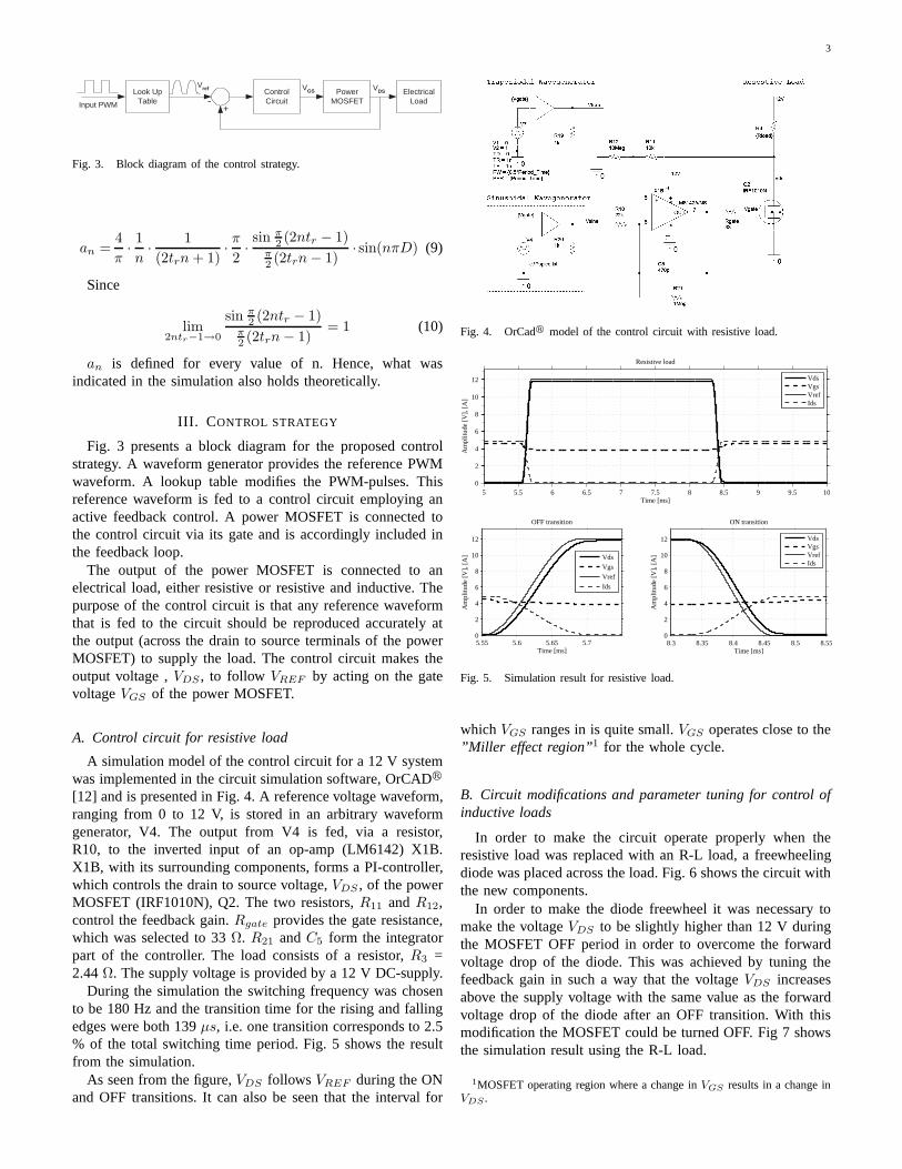
3
V DS Look Up Table
Control Circuit
Power MOSFET
Electrical Load Input PWM
V ref V GS
- +
Fig. 3. Block diagram of the control strategy.
an =4
π· 1
n· 1
(2trn + 1)· π2· sin π
2(2ntr − 1)
π2(2trn − 1)
· sin(nπD) (9)
Since
lim2ntr−1→0
sin π2(2ntr − 1)
π2(2trn − 1)
= 1 (10)
an is defined for every value of n. Hence, what wasindicated in the simulation also holds theoretically.
III. C ONTROL STRATEGY
Fig. 3 presents a block diagram for the proposed controlstrategy. A waveform generator provides the reference PWMwaveform. A lookup table modifies the PWM-pulses. Thisreference waveform is fed to a control circuit employing anactive feedback control. A power MOSFET is connected tothe control circuit via its gate and is accordingly includedinthe feedback loop.
The output of the power MOSFET is connected to anelectrical load, either resistive or resistive and inductive. Thepurpose of the control circuit is that any reference waveformthat is fed to the circuit should be reproduced accurately atthe output (across the drain to source terminals of the powerMOSFET) to supply the load. The control circuit makes theoutput voltage ,VDS , to follow VREF by acting on the gatevoltageVGS of the power MOSFET.
A. Control circuit for resistive load
A simulation model of the control circuit for a 12 V systemwas implemented in the circuit simulation software, OrCADr
[12] and is presented in Fig. 4. A reference voltage waveform,ranging from 0 to 12 V, is stored in an arbitrary waveformgenerator, V4. The output from V4 is fed, via a resistor,R10, to the inverted input of an op-amp (LM6142) X1B.X1B, with its surrounding components, forms a PI-controller,which controls the drain to source voltage,VDS , of the powerMOSFET (IRF1010N), Q2. The two resistors,R11 and R12,control the feedback gain.Rgate provides the gate resistance,which was selected to 33Ω. R21 andC5 form the integratorpart of the controller. The load consists of a resistor,R3 =2.44Ω. The supply voltage is provided by a 12 V DC-supply.
During the simulation the switching frequency was chosento be 180 Hz and the transition time for the rising and fallingedges were both 139µs, i.e. one transition corresponds to 2.5% of the total switching time period. Fig. 5 shows the resultfrom the simulation.
As seen from the figure,VDS follows VREF during the ONand OFF transitions. It can also be seen that the interval for
Fig. 4. OrCadr model of the control circuit with resistive load.
5 5.5 6 6.5 7 7.5 8 8.5 9 9.5 100
2
4
6
8
10
12
Resistive load
Time [ms]
Am
plitu
de [V
], [A
]
VdsVgsVrefIds
5.55 5.6 5.65 5.70
2
4
6
8
10
12
OFF transition
Time [ms]
Am
plitu
de [V
], [A
]
Vds
Vgs
Vref
Ids
8.3 8.35 8.4 8.45 8.5 8.550
2
4
6
8
10
12
ON transition
Time [ms]A
mpl
itude
[V],
[A]
VdsVgsVrefIds
Fig. 5. Simulation result for resistive load.
which VGS ranges in is quite small.VGS operates close to the”Miller effect region”1 for the whole cycle.
B. Circuit modifications and parameter tuning for control ofinductive loads
In order to make the circuit operate properly when theresistive load was replaced with an R-L load, a freewheelingdiode was placed across the load. Fig. 6 shows the circuit withthe new components.
In order to make the diode freewheel it was necessary tomake the voltageVDS to be slightly higher than 12 V duringthe MOSFET OFF period in order to overcome the forwardvoltage drop of the diode. This was achieved by tuning thefeedback gain in such a way that the voltageVDS increasesabove the supply voltage with the same value as the forwardvoltage drop of the diode after an OFF transition. With thismodification the MOSFET could be turned OFF. Fig 7 showsthe simulation result using the R-L load.
1MOSFET operating region where a change inVGS results in a change inVDS .
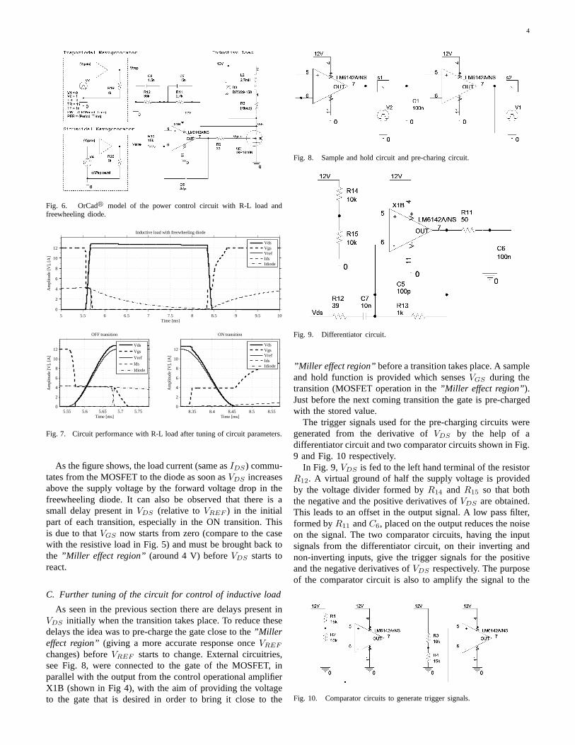
4
Fig. 6. OrCadr model of the power control circuit with R-L load andfreewheeling diode.
5 5.5 6 6.5 7 7.5 8 8.5 9 9.5 100
2
4
6
8
10
12
Inductive load with freewheeling diode
Time [ms]
Am
plitu
de [V
], [A
]
VdsVgsVrefIdsIdiode
5.55 5.6 5.65 5.7 5.750
2
4
6
8
10
12
OFF transition
Time [ms]
Am
plitu
de [V
], [A
]
Vds
Vgs
Vref
Ids
Idiode
8.35 8.4 8.45 8.5 8.550
2
4
6
8
10
12
ON transition
Time [ms]
Am
plitu
de [V
], [A
]
VdsVgsVrefIdsIdiode
Fig. 7. Circuit performance with R-L load after tuning of circuit parameters.
As the figure shows, the load current (same asIDS) commu-tates from the MOSFET to the diode as soon asVDS increasesabove the supply voltage by the forward voltage drop in thefreewheeling diode. It can also be observed that there is asmall delay present inVDS (relative toVREF ) in the initialpart of each transition, especially in the ON transition. Thisis due to thatVGS now starts from zero (compare to the casewith the resistive load in Fig. 5) and must be brought back tothe ”Miller effect region” (around 4 V) beforeVDS starts toreact.
C. Further tuning of the circuit for control of inductive load
As seen in the previous section there are delays present inVDS initially when the transition takes place. To reduce thesedelays the idea was to pre-charge the gate close to the”Millereffect region” (giving a more accurate response onceVREF
changes) beforeVREF starts to change. External circuitries,see Fig. 8, were connected to the gate of the MOSFET, inparallel with the output from the control operational amplifierX1B (shown in Fig 4), with the aim of providing the voltageto the gate that is desired in order to bring it close to the
Fig. 8. Sample and hold circuit and pre-charing circuit.
Fig. 9. Differentiator circuit.
”Miller effect region” before a transition takes place. A sampleand hold function is provided which sensesVGS during thetransition (MOSFET operation in the”Miller effect region” ).Just before the next coming transition the gate is pre-chargedwith the stored value.
The trigger signals used for the pre-charging circuits weregenerated from the derivative ofVDS by the help of adifferentiator circuit and two comparator circuits shown in Fig.9 and Fig. 10 respectively.
In Fig. 9,VDS is fed to the left hand terminal of the resistorR12. A virtual ground of half the supply voltage is providedby the voltage divider formed byR14 and R15 so that boththe negative and the positive derivatives ofVDS are obtained.This leads to an offset in the output signal. A low pass filter,formed byR11 andC6, placed on the output reduces the noiseon the signal. The two comparator circuits, having the inputsignals from the differentiator circuit, on their inverting andnon-inverting inputs, give the trigger signals for the positiveand the negative derivatives ofVDS respectively. The purposeof the comparator circuit is also to amplify the signal to the
Fig. 10. Comparator circuits to generate trigger signals.

5
5.55 5.6 5.65 5.7
0
5
10
OFF transitionA
mpl
itude
[V]
t [ms]
VDS
VDSPreCharge
8.35 8.4 8.45
0
5
10
OFF transition
Am
plitu
de [V
]
t [ms]
VDS
VDSPreCharge
5.56 5.57 5.58 5.590
1
2
3
Am
plitu
de [V
]
t [ms]8.34 8.35 8.36 8.37 8.38
10
10.5
11
11.5
12
12.5A
mpl
itude
[V]
t [ms]
Fig. 11. Comparison ofVDS performance without and with the”pre-charging” circuit.
supply voltage level.In Fig. 11 a comparison of two simulations are presented
with and without ”pre-charging” circuits. As can be notedfrom the figure, the delays are substantially reduced.
There is another important advantage with this set-up. The”Miller effect region” varies with temperature and also variesfrom MOSFET to MOSFET. With the used set-up, the circuitnow provide a great flexibility, since it becomes self-adjusting.
IV. A NALYSIS ON SWITCHING LOSSES FROM SIMULATION
FOR RESISTIVE LOAD
By using the method proposed in [5], [6] and [7], i.eto increase the gate resistance in order to obtain a ”softer”transition, the switching losses in the MOSFET increases.Accordingly, an important aspect is to investigate how theswitching losses are affected when the trapezoidal transitionis changed to a sinusoidal one.
For a resistive load the current transition is sinusoidal aswell as the voltage transition. The voltage and current OFFtransition can be described as:
vsine(ωt) = v · 1 − cos(ωt)
2, 0 ≤ ωt ≤ π (11)
isine(ωt) = i · 1 + cos(ωt)
2, 0 ≤ ωt ≤ π (12)
For the linear OFF transition for a trapezoidal pulse withsame transition time as the sinusoidal the voltage and currentcan be written as:
vtrap(ωt) =v
π· ωt, 0 ≤ ωt ≤ π (13)
itrap(ωt) = i ·[
1 − 1
πωt
]
, 0 ≤ ωt ≤ π (14)
Fig. 12 shows the linear and sinusoidal OFF transitions withcorresponding instantaneous switching power losses.
0 0.5 1 1.5 2 2.5 3
0
0.2
0.4
0.6
0.8
1
Trapezoidal TransitionVoltage and Current
Am
plitu
de [p
.u.]
ωt [rad]
Voltage
Current
0 0.5 1 1.5 2 2.5 3
0
0.2
0.4
0.6
0.8
1
Sinusoidal TransitionVoltage and Current
Am
plitu
de [p
.u.]
ωt [rad]
Voltage
Current
0 0.5 1 1.5 2 2.5 30
0.1
0.2
0.3
Trapezoidal TransitionPower Losses
Am
plitu
de [p
.u.]
ωt [rad]0 0.5 1 1.5 2 2.5 3
0
0.1
0.2
0.3
Sinusoidal TransitionPower Losses
Am
plitu
de [p
.u.]
ωt [rad]
Fig. 12. Linear and sinusoidal OFF transition with corresponding instanta-neous switching losses.
The total switching loss for one transition, linear andsinusoidal, is given by:
Psine =
∫ π
ωt=0
vsine(ωt) · isine(ωt) dωt =viπ
8(15)
Ptrap =
∫ π
ωt=0
vtrap(ωt) · itrap(ωt) dωt =viπ
6(16)
As seen from (16) and (15) the switching losses can bereduced by 25 % theoretically when going from the lineartransition to the sinusoidal transition for a resistive loading.
Fig. 13 shows the corresponding switching losses for one offtransition obtained from simulation using the control circuit inFig. 4. The transition time was set to 139µs and the load usedwas a 2.44Ω resistance. The switching losses were given asthe product of the voltageVDS and the currentIDS throughthe MOSFET. As seen from Fig. 13 the behavior of the powerlosses is similar as for the theoretical case (refer Fig. 12). Theswitching losses for the linear transition was 9.2 W whereasthe sinusoidal gave 7.2 W, so the losses where reduced byroughly 23 %, almost same as the theoretical result showed.
V. M EASUREMENTS AND ANALYSIS
A. Practical test setup
An experimental circuit was built based on the simulationmodel shown in Fig. 4. A Complex Programmable LogicDevice (CPLD (XC2C256)) mounted on a design kit [13]worked as the reference voltage waveform generator as seenin Fig. 14. The reference waveform was stored as an 8-bitlookup table in the CPLD. An 8-bit D/A-converter (HI5660IB)connected to the CPLD converts this digital data to an analogreference signal.
A voltage reference level, obtained as a scaled value of themain supply, controls the maximum amplitude of the referencesignal. The lookup table in the CPLD is triggered from anexternal PWM reference pulse coming from a signal generator.

6
5.55 5.6 5.65 5.7
2
4
6
8
10
12
Trapezoidal TransitionVoltage and Current
Time [ms]
Am
plitu
de [V
], [A
]
Voltage
Current
5.55 5.6 5.65 5.7
2
4
6
8
10
12
Sinusoidal TransitionVoltage and Current
Time [ms]
Am
plitu
de [V
], [A
]
Voltage
Current
5.55 5.6 5.65 5.7
2
4
6
8
10
12
14
Trapezoidal TransitionPower Losses
Pow
er [W
]
Time [ms]5.55 5.6 5.65 5.7
2
4
6
8
10
12
14
Sinusoidal TransitionPower Losses
Pow
er [W
]
Time [ms]
Fig. 13. Linear and sinusoidal OFF transition with corresponding instanta-neous switching losses obtained from simulations in OrCadr for a resistiveloading.
Fig. 14. The CPLD kit along with the power control circuit.
Every time the PWM signal changes its state from low tohigh or vice versa, the lookup table is triggered to feed outthe stored values counting up or down respectively. The D/Aconverter converts the data from the lookup table into ananalog signal, which is fed as the reference voltage to thecontrol circuit. An external signal generator was used to supplythe PWM pattern.
Regarding the control circuit, a few modifications fromthe simulation model were considered. The feedback resistorsfor the control op-ampR11 and R12 as seen in Fig. 4were exchanged with trim pots and some EMI suppressioncapacitors were placed at strategic positions in the circuit. Theload consists of 16 power resistors connected in parallel, eachone of them having a resistance of 39Ω, giving an equivalentresistance of 2.44Ω, same as for the simulation model withthe resistive load.
L m R m
MOSFET
G
S
D
freewheeling diode
+V
+
- LM6144
PWM
+V
S w R 1
R 5 R 4
R 2
R 3
C 2
C 3
C 1
X1
+V
Fig. 15. Control op-amp with extra-switched feedback control.
B. Different feedback gains for ON and OFF transitions
While tuning the practical circuit, it was found that forsmooth transitions during both the ON and the OFF transitions,different feedbacks were required. A resistive divider governsthe feedback gain, for the control op-amp. By putting a seriescombination of a trim pot and a switch in parallel with one ofthe feedback resistors, the gain could be adjusted in order toobtain two different suitable values. Fig. 15 shows the circuitachieving this switching.
C. Frequency response of output voltage from measurementswith resistive load
In this section a comparison between the trapezoidal andsinusoidal pulses is presented based on practical measurementsfor resistive load. The system clock used for the CPLDwas 1.8432 MHz, making the transition time to be 139µs.Considering the transition times to be 2.5 % of the totalswitching time period, the switching frequency employed was180 Hz and the duty cycle was set to 50 % on the signalgenerator. The frequency response was obtained by using adynamic signal analyser with a sampling frequency of 250kHz. The dynamic signal analyser presents the frequencyspectrum up till 100 kHz from the FFT of the measured signal.For each measurement, an average of 100 FFTs was taken inorder to reduce the effect of the background noise level2. Fig.16 compares the frequency spectrum of the measured outputvoltage using sinusoidal transitions and trapezoidal shapedpulses [10].
As can be seen from the measurements, the two voltagereferences have the same slopes of the frequency spectrumenvelope in the low frequency region, which is around -22 dB/decade. The envelope of the trapezoidal waveformfalls after a cut-off frequency of 3 kHz with a slope of -48dB/decade. The envelope of the sinusoidal waveform falls aftera cut-off frequency of 4.5 kHz with a slope of -67 dB/decade.
The theoretical study, where the sinusoidal waveform wascompared with the trapezoidal as seen in Fig. 1, showed that
2The envelope of the frequency spectrum is the major concern,and hencethe average mode is a very well motivated method to be employed
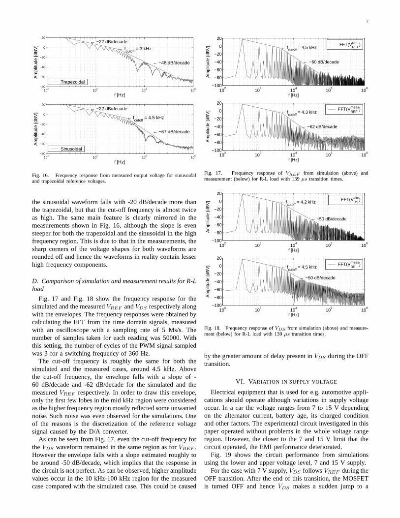
7
102
103
104
105
−80
−60
−40
−20
0
20
f [Hz]
Am
plitu
de [d
BV
]
← fcutoff
= 3 kHz
← −22 dB/decade
← −48 dB/decade
Trapezoidal
102
103
104
105
−80
−60
−40
−20
0
20
f [Hz]
Am
plitu
de [d
BV
]
← fcutoff
= 4.5 kHz
← −22 dB/decade
← −67 dB/decade
Sinusoidal
Fig. 16. Frequency response from measured output voltage for sinusoidaland trapezoidal reference voltages.
the sinusoidal waveform falls with -20 dB/decade more thanthe trapezoidal, but that the cut-off frequency is almost twiceas high. The same main feature is clearly mirrored in themeasurements shown in Fig. 16, although the slope is evensteeper for both the trapezoidal and the sinusoidal in the highfrequency region. This is due to that in the measurements, thesharp corners of the voltage shapes for both waveforms arerounded off and hence the waveforms in reality contain lesserhigh frequency components.
D. Comparison of simulation and measurement results for R-Lload
Fig. 17 and Fig. 18 show the frequency response for thesimulated and the measuredVREF andVDS respectively alongwith the envelopes. The frequency responses were obtained bycalculating the FFT from the time domain signals, measuredwith an oscilloscope with a sampling rate of 5 Ms/s. Thenumber of samples taken for each reading was 50000. Withthis setting, the number of cycles of the PWM signal sampledwas 3 for a switching frequency of 360 Hz.
The cut-off frequency is roughly the same for both thesimulated and the measured cases, around 4.5 kHz. Abovethe cut-off frequency, the envelope falls with a slope of -60 dB/decade and -62 dB/decade for the simulated and themeasuredVREF respectively. In order to draw this envelope,only the first few lobes in the mid kHz region were consideredas the higher frequency region mostly reflected some unwantednoise. Such noise was even observed for the simulations. Oneof the reasons is the discretization of the reference voltagesignal caused by the D/A converter.
As can be seen from Fig. 17, even the cut-off frequency fortheVDS waveform remained in the same region as forVREF .However the envelope falls with a slope estimated roughly tobe around -50 dB/decade, which implies that the response inthe circuit is not perfect. As can be observed, higher amplitudevalues occur in the 10 kHz-100 kHz region for the measuredcase compared with the simulated case. This could be caused
102
103
104
105
106
−100
−80
−60
−40
−20
0
20
f [Hz]
Am
plitu
de [d
BV
] ← fcutoff
= 4.5 kHz
← −60 dB/decade
FFT(VREFsim )
102
103
104
105
106
−100
−80
−60
−40
−20
0
20
f [Hz]
Am
plitu
de [d
BV
] ← fcutoff
= 4.3 kHz
← −62 dB/decade
FFT(VREFmeas)
Fig. 17. Frequency response ofVREF from simulation (above) andmeasurement (below) for R-L load with 139µs transition times.
102
103
104
105
106
−100
−80
−60
−40
−20
0
20
f [Hz]
Am
plitu
de [d
BV
] ← fcutoff
= 4.2 kHz
← −50 dB/decade
FFT(VDSsim)
102
103
104
105
106
−100
−80
−60
−40
−20
0
20
f [Hz]
Am
plitu
de [d
BV
] ← fcutoff
= 4.5 kHz
← −50 dB/decade
FFT(VDSmeas)
Fig. 18. Frequency response ofVDS from simulation (above) and measure-ment (below) for R-L load with 139µs transition times.
by the greater amount of delay present inVDS during the OFFtransition.
VI. VARIATION IN SUPPLY VOLTAGE
Electrical equipment that is used for e.g. automotive appli-cations should operate although variations in supply voltageoccur. In a car the voltage ranges from 7 to 15 V dependingon the alternator current, battery age, its charged conditionand other factors. The experimental circuit investigated in thispaper operated without problems in the whole voltage rangeregion. However, the closer to the 7 and 15 V limit that thecircuit operated, the EMI performance deteriorated.
Fig. 19 shows the circuit performance from simulationsusing the lower and upper voltage level, 7 and 15 V supply.
For the case with 7 V supply,VDS follows VREF during theOFF transition. After the end of this transition, the MOSFETis turned OFF and henceVDS makes a sudden jump to a

8
5.5 5.6 5.7 5.80
2
4
6
87 V supply
t [ms]
VREF
[V]V
DS [V]
5.5 5.6 5.7 5.80
5
10
15
15 V supply
t [ms]
VREF
[V]V
DS [V]
Fig. 19. Simulation of the control circuit for supply voltage of 7 and 15 V.
level equal to the supply voltage plus the forward voltage droprequired for the freewheeling diode. The jump inVDS will giverise to unwanted EMI noise.
For the case with 15 V supply,VDS does not complete afull sinusoidal OFF transition, but is instead interruptedat themaximum voltage level.
In order to achieve a smooth transition independently ofthe present supply voltage, the feedback gain should havebeen tuned accordingly. It should be pointed out that this isaminor problem. The fact that the main function, i.e. obtaininga PWM-switched voltage, still is working without problems,isthe most important issue in the case of a large voltage deviationfrom the ideal one. However, the results show that there isa need for further development if the lowest possible EMIperformance is desired also at the upper and lower voltagelimits.
VII. C ONCLUSION
In this paper theoretical and experimental studies show thatby employing smooth transitions in DC/DC converters, theEMI from a switching converter can be reduced. A flexiblecurve shaping circuit was developed and implemented forcontrol of resistive and R-L loads for a 12 V system. A methodof employing pre-charging of the gate of a switching MOSFETis investigated and implemented with the aim of reducingdelays presented in switching voltage. Results from theoreticalanalysis and simulations showed that sinusoidal transition is abeneficial choice compared to a linear transition, both in termsof reduction in EMI and lowering the switching losses (at leastfor a resistive loading case).
REFERENCES
[1] Y. Shrivastava, S. Y. Hui, S. Sathiakumar, H. S. Chung, and K. K. Tse,Harmonic Analysis of Nondeterministic Switching Methods for DC/DCPower Converters, IEEE Trans. Circuits Syst., vol. 47, pp. 868-883, June2000.
[2] K. K. Tse, H. S. Chung, S. Y. R. Hui, and H. C. So,A ComparativeInvestigation on the Use of Random Modulation Schemes for DC/DCConverters, IEEE Trans. Ind. Electron., vol. 47, pp. 253-263, Apr. 2000.
[3] Divan, D.M., The resonant DC link converter-a new concept in staticpower conversion; Industry Applications, IEEE Transactions on , Vol-ume: 25 , Issue: 2 , March-April 1989 pp:317-325
[4] Ned Mohan, Tore Undeland, William Robbins,Power Electronics: Con-verters, Applications and Design, 2 nd Edition, John Wiley & Sons Inc.,ISBN 0-471-58408-8
[5] A. Consoli, S. Musumeci, G. Oriti, A. Testa.”Conducted EmissionImprovement of Modern Gate Controlled Devices”, Proceedings ofNinthInternational Conference on Electromagnetic Compability, September 5-7, 1994, Manchester, UK
[6] A. Consoli, S. Musumeci, G. Oriti, A. Testa.”An Innovative EMIReduction Design Technique in Power Converters”, Proceedings ofInter-national Symposium on Electromagnetic Compability, September 13-16,1994, Roma, Italy
[7] S. Musumeci, G. Oriti, G. Scarcella, A. Testa, A. Consoli. ”Optimizationof Switching Losses and EMI in a Cuk converter”, Proceedings ofPower Electronics, Drives and Energy Systems for Industrial Growth,Proceedings of the 1996 International Conference on , Volume: 2 , 8-11Jan. 1996 Pages:807 - 812 vol.2, September 13-16, 1994, Roma, Italy.
[8] H. Sawezyn, N. Idir, R. Bausiere”Lowering the Drawbacks of Slowingdowndi/dt anddv/dt of Insulated Gate Transistors”, Power Electronics,Machines and Drives, 2002. International Conference on (Conf. Publ. No.487) , 4-7 June 2002 Pages:551-556.
[9] H.P. Yee. ”An EMI suppression MOSFET driver”, Applied PowerElectronics Conference and Exposition, 1997. APEC ’97 ConferenceProceedings 1997., Twelfth Annual , Volume: 1 , 23-27 Feb. 1997 pp:242-248 vol.1.
[10] Henrik Holst, Himashu Jain, Torbjrn Thiringer, Tryggve Tuveson,Re-duction of RF-emissions from a Pulsed Electrical Supply using an ActiveGate Control, Paper No 070, NORPIE June 2004, NTNU, Norway
[11] Henrik Holst, Pravin Futane,Reduction of EMI in Switched ModeConverters by Shaped Pulse Transitions and its Applicationto HybridElectric Vehicles, Chalmers University of Technology 2004, ISSN 1401-6176, Report No. 32R.
[12] Cadence Design Systems, Inc. 2006, PSpicer . An OrCADr familyproduct providing industry-standard solutions for accurate analog andmixed-signal simulations. URL: http://www.cadence.com/orcad/
[13] Xilinx Corporation (2003), XC2C256 Coolrunner-II CPLD: Design kit.URL: http://www.xilinx.com/cpld/
