mos sc filters
DESCRIPTION
SC FiltersTRANSCRIPT

PROCEEDINGS OF THE IEEE, VOL. 67, NO. 1 , JANUARY 1979 61
MOS Switched-Capacitor Filters
Invited Paper
Abstmct-In the past sevd yeas, much progress has been made in bringing the economies of integrated-circuit technology to bear on the realization of voiceband frequency selective biters. This paper will re- view one approach to this problem, the use of switched-capacitor tech- niqueg n e paper emphasizes the practical aspects of switched-capacitor filter design under the constraints imposed by MOS mmted-circuit technology. The basic operation of switched-capacitor filters is re- viewed, followed by a discussion of the properties of the various cir- cuit building blocks m MOS technology. Finally, a of several flter orgpoiptions which appear to be wen suited to santched-capacitor implementation is presented.
I. INTRODUCTION
F REQUENCY selective analog filtering has long evaded the efforts of technologists and designers to develop filter realizations which can be completely integrated on a sili-
con chip. The development of low-cost high-performance monolithic operational amplifiers led to the utilization of active-RC filtering techniques to Teplace passive RLC filters in the 1960's. Classical RC-active filters have proven difficult to realize in completely monolithic form because stable pre- cise RC products cannot be achieved in standard monolithic processes. As a result, the preferred technological approach to voice-frequency analog filtering until very recently has been discrete component or hybrid integrated-circuit realizations of various types of active filters. Recent developments in mono- lithic circuit techniques offer the possibility of fully integrat- ing the voice-frequency filtering function, with resultant savings in manufacturing cost. One of these techniques, the switched- capacitor approach, is the subject of this paper.
This technique makes use of the unique properties of metal- oxide-semiconductor (MOS) integrated-circuit technology. This technology has become widely used in the realization of digital LSI circuits because of its superior logic density, which arises from the fact that, in contrast to bipolar, the MOS tran- sistor is self-isolating. While the density advantage of MOS has led to its wide utilization for digital circuits, a second-key advantage, which has only recently been recognized, has led to the increasing use of MOS technology to perform analog signal processing. In contrast to bipolar technology, MOS integrated circuits offer the ability to store charge on a node over a period of many milliseconds and to sense the value of the charge continuously and nondestructively. The former results from the high impedance of the MOS transistor in the off state, and the latter results from the essentially infinite input impedance of the MOS transistor in the active mode of
research w a s supported by DARPA and monitored by NRL under Con- Manuscript received June 17, 1978;revised September 21 ,1978 . The
tract N000173-77-C-0238. The authors are with the Department of Electrical Engineering and
Computer Sciences and the Electronics Research Laboratory, Uni- versity of California, Berkeley, CA 94720.
operation. This inherent analog memory capability does not exist in bipolar technology because the recombination current associated with the flow of minority carriers in a bipolar tran- sistor rapidly discharges the small capacitance on which the voltage information is stored.
The charge storage feature of MOS technology was first utilized in dynamic random-access memory design and dy- namic logic. In both instances, information storage on small nodal capacitances in the circuit allows the elimination of active or pullup transistors which are otherwise required to preserve the information content of the circuit. This results in greater circuit density. While the information stored on nodal capacitance is essentially analog in that the node voltage has a continuous range of Values, in digital applications the in- formation is usually interpreted as being only one of two logic levels; these binary levels are typically refreshed (restored) every two milliseconds.
The charge storage feature of MOS technology was first used to perform analog signal processing with the advent of the bucket brigade shift register. In this device, a time-vary- ing analog signal is converted to a series of charge packets, proportional to the value of the input signal at the sample instants. These charge packets are passed serially through a chain of MOS capacitors, the motion of the charge being brought about by the action of appropriately clocked MOS devices. In analog filtering applications of such devices, the charge at each capacitor site is sensed nondestructively by MOS transistors. These sensed voltages can, for example, be added in a weighted summation to produce a single output, providing realization of sampled-data transversal filter [ 1 1.
The charge-coupled device (CCD), which was developed subsequent to the bucket brigade, provides a similar func- tion in analogsignal processing applications, but with the in- tegration of the storage capacitance with the MOS switch structure and MOS sensing device in such a way that trans- versal fiters and other analog signal processing devices can be fabricated in a smaller silicon area and achieve higher per- formance. These devices provide an extremely effective tech- nological tool for attacking filtering problems in which trans- versal filter structures are required, for example as matched and adaptive filters [ 21.
However, the utilization of CCD and bucket-brigade filters in large-quantity low-cost general filtering applications has been hindered by several factors. First, until very recently, the peripheral circuitry required to convert the input signal into charge packets and to recover a low-impedance voltage signal at the output had to be realized off-chip since this circuitry was not thought to be easily realizable on the same chip. Second, the transversal filter itself has certain limita- tions as a general-purpose analog filtering and signal process-
0018-9219/79/0100-0061$00.75 0 1979 IEEE

62 PROCEEDINGS OF THE IEEE, VOL. 67, NO. 1, JANUARY 1979
IN
Fig. 1. A second-order direct form discrete time filter.
1 ‘ t t
i _ _ _ _ i L _ _ _ _ _ - I i - - - - - I MULTIPLY8 DELAY 1 MULTIPLY 8 DELAY SUM 6 HOLD 1-
Fig. 2 . Analog sampled data realization of,the filter shown in Fig. 1 using MOS switches, capacitors, and operational amplifiers.
ing technique. Among these is the fact that since the signal is time sampled at the input to the CCD, a continuous-time antialiasing filter is required to bandlimit the input signal to a frequency below the sampling rate. Since the sampling rate in CCD’s must be relatively low (to minimize filter length and conserve silicon area) a relatively complex anti-aliasing filter is required. Also, since CCD filters are nonrecursive, for transfer functions with a narrow passband which have long impulse responses, a very long CCD filter utilizing large silicon area is required.
In the last two years, the concept of analog charge storage and processing in MOS technology has been applied in new ways and has overcome some of the difficulties inherent in the transversal filter structures. First, in order to obtain highly selective filters with long impulse responses in a small silicon area, one is led to adopt a recursive filter structure. The classical second-order recursive filter section, shown in Fig. 1, requires two delay elements (shown as a D) and four multipli- cation elements with factors which can be greater than unity. While a passive charge-coupled structure can realize the delays, an active amplifier of some type must be used to provide gain. This second-order recursive section can perhaps be most ef- ficiently realized by simply using two capacitive delay elements together with several amplifiers as shown in Fig. 2 [ 3 1, [4]. This structure has the advantage that infinitely long impulse responses can be obtained, but it suffers from the disadvantage that as one attempts to make the sampling rate higher to ease the anti-aliasing requirements, the sensitivity of the filter re- sponse to variation in the parameters al and a2 becomes larger. Since in an analog recursive filter like the one shown in Fig. 2, these coefficients are realized using ratioed passive compo- nents, a severe practical limitation is imposed on the range of sample rates and the selectivity of responses obtainable from analog realizations of these filters.
The recursive section of Fig. 2 consists of analog switches, operational amplifiers, and capacitors. These same elements
(a) (b) Fig. 3. (a) A switched-capacitor which in many cases can simulate the
shown in part (a). function of a resistor. (b) An MOS implementation of the circuit
can be rearranged to provide many alternate filtering con- figurations with sensitivity properties more closely resembling those of continuous-time filters in the limit of high sampling rates. These filters have come to be called switched-capacitor filters, and are distinguished by the fact that they utilize a capacitor and MOS switches to simulate the circuit behavior ofaresistor,asshowninFig.3 [ S I - [ 7 ] .
The operation of this “resistor” is as follows: the switch is initially in the left-hand position so that the capacitor C is charged to the voltage VI. The switch is then thrown to the right and the capacitor is discharged to the voltage V2. The amount of charge which flows into (or from) V2 is thus Q = C( Vz - VI ). If the switch is thrown back and forth at a clock rate f,, then the average current flow i from VI into Vz will be C(V2 - Vl)f,. Thus the size of an equivalent resistor which would give the same average current as this circuit is
R = l/Cfc.
If the switched time is much larger than the signal frequencies of interest then the time sampling of the signal which occurs in this circuit can be ignored in a first-order analysis and the switched capacitor can often be considered as a direct replace- ment for a conventional resistor. If, however, the switch rate and signal frequencies are of the same order then sampled data techniques are required for analysis and, as for any sampled data system, the input signal should be bandlimited as dic- tated by the sampling theorem.
Note that we have assumed that VI and Vz are voltage sources, and that the values of VI and Vz are not affected by the switch closures. While this is in effect true in the filters to be described in this paper, which are based on switched- capacitor integrators, it is not true in more general circuits containing capacitors and switches. In these cases simple sub- stitution of switched capacitors for resistors can give results different from the continuous case.
The switched-capacitor resistors require very little silicon area to implement large resistance values. In fact the silicon area decreases as the required value of resistance increases. To implement audio-frequency filters a resistance on the order of 10 Ma is needed if a monolithic capacitor of a reasonable size is to be used (-10 pF). This value of resistance is easily achieved by switching a I-pF capacitor at 100-kHz rate, re- quiring approximately a silicon area of 0.01 mmz (to be com- pared to a total chip area of 10-20 mm2). If a 1 O-MQ resistor were implemented by using a polysilicon line or diffusion the area required would be at least 100 times larger.
By using this switched-capacitor resistor in conjunction with other capacitors and op amps it is possible to realize many of the circuit configurations used in conventionalRCactive filters. As in the case of the recursive filter of Fig. 1 and the charge- transfer device (CTD) filters, the signal in switched-capacitor filters is sampled in time so that an antialiasing filter is re- quired. However, in contrast to the circuit of Fig. 2, as the

BRODERSEN e t al . : MOS SWITCHED-CAPACITOR FILTERS 63
c ' 'T f c z & g (b)
Fig. 4. (a) A single-pole RC continuous low-pass fiiter. (b) Single-pole low-pass filter utilizing a switched-capacitor resistor.
sampling rate is increased the sensitivities generally decrease to those of the continuous-time RC-active counterpart. Also the penalty in silicon area for a high sample rate is much less in the switched-capacitor filters in comparison to the CTD transversal filters.
Viewed from a conventional RC-active filter standpoint, these filters have the property, which will be demonstrated below, that all the RC time constants of the filter are deter- mined by the clock frequency which is used to drive the switches and by capacitor ratios. Thus the problem of con- trolling RC products to a high degree of accuracy, which is characteristic of RC-active filter realizations, is reduced for these filters to the problem of maintaining accurate capacitor ratios and supplying an accurate external clock frequency. This property makes the filters much more practical for mono- lithic realization.
A conventional single-pole RC-low-pass filter is shown in Fig. 4(a), and a switched-capacitor implementation of this filter is shown in Fig. 4(b). In spite of the simplicity of this filter it demonstrates some of the most important advantages of the use of switched-capacitors. The 3-dB bandwidth of the conventional RC filter is
The 3-dB width of the switched-capacitor fiter can be found approximately by substituting the effective resistance of the switched capacitor C1 into (1) to obtain
(The constraint that fc >> O%B is imposed in order that the effect of time sampling and charge sharing can be ignored.) Since the bandwidth of the switched-capacitor filter is pro- portional to a ratio of capacitor values, it can be accurately defined with a high degree of stability.
From (3) it can be seen that WEB is proportional to the clock frequency; thus programmability can be achieved by simply varying the clock rate (a property which is common to all discrete time filters).
If one were restricted to the use of passive components and switches as in the case of Fig. 4(b), a very limited class of filter responses would be possible. It is possible, however, to design MOS operational amplifiers that can be used with switches and capacitors so as to extend greatly the capability of the filters. In the next section the limitations of the MOS technology and its relation to switched-capacitor filter cir- cuits will be descrjbed.
11. PROPERTIES OF MOS SWITCHES, CAPACITORS, AND OPERATIONAL AMPLIFIERS
The properties of MOS technology and the switched-capaci- tor resistors place significant limitations on the range of real- izable filter configurations. In this section these limitations are explored.
A. MOS Capacitors The MOS transistor itself is essentially a nonlinear capacitor
in which the charge induced on one plate by the applied volt- age forms the conducting channel of the transistor. The di- electric of this capacitor is silicon dioxide, which is one of the most stable dielectrics known. However, the MOS tran- sistor itself is not particularly useful as a capacitor because of its inherently nonlinear behavior. Within an MOS integrated circuit, capacitors which have a sufficiently low-voltage coef- ficient to be useful as precision passive components are gener- ally made in one of several ways:
1) Metal-Oxide-Crystalline Silicon Capacitors: This struc- ture is formed by utilizing a heavily doped (low-resistance) re- gion in the silicon substrate as the capacitor back plate, and the interconnect metallization (usually aluminum) as the top plate. This particular capacitor type is best suited to metal- gate CMOS and MOS processes which do not use self-alignment procedures and can thus realize the capacitors directly without process modifications.
2) Polysilicon-Oxide-Polysilicon Capacitors: In this capaci- tor structure, the two plates of the capacitor are formed of two separate layers of polysilicon (deposited polycrystalline silicon). This capacitor structure is best suited to silicon gate NMOS and CMOS processes having two polysilicon layers, which can realize these capacitance structures without extra process steps.
3) Other Capacitance Structures: By including extra mask- ing steps, any combination of silicon substrate, polysilicon layer, and metallization layer can be used as the plates of the capacitors. However, such structures are only needed in sili- con gate processes which have only one layer of polysilicon.
These capacitance structures tend to have common charac- teristics, From the standpoint of switched-capacitor filters, the most important of these characteristics are:
a) Ratio accuracy: A key aspect of the performance of any frequency-selective filter is the accuracy and reproducibil- ity of the frequency response. For switched-capacitor filters this requires a certain level of accuracy in the ratios of capaci- tors. Integrated MOS capacitors have a value which is deter- mined by the dielectric constant, the thickness of the dielec- tric, and the area of the capacitor. Assuming that the dielectric constant and thickness do not vary, the ratio of two capacitors made within the same integrated circuit will depend only on their area ratio. This is primarily determined by the geometri- cal shape of the capacitors defined by the photolithographic mask used to make the integrated circuit.
Errors in the geometrically defined ratio occur because the actual definition of the capacitor is done optically, which re- sults in errors in the capacitor edge location due to the finite wavelength of the light used and the control of the chemical or plasma etching of the metallization and, in addition, be- cause the thickness of the dielectric can vary with distance across the integrated circuit. These effects can be alleviated with careful layout of the components and the errors gen- erally get smaller as the capacitor dimensions are made larger. Generally speaking, the achievable ratio accuracies range from

64 PROCEEDINGS OF THE IEEE, VOL. 67, NO. 1 , JANUARY 1979
1-2 percent for small capacitor geometries (-400 pm') t o on the order of 0.1 percent for capacitor geometries which ap- proach the limit of economical size (40 000 pm2) [8]. This also implies that as the capacitance ratio gets larger, the achiev- able accuracy in a given area decreases since the smaller of the two capacitors must be decreasing.
b) Voltage coefficient and temperature coefficient: MOS capacitors made with heavily doped silicon plates display volt- age coefficients in the range of 10 to 100 ppm/V. Tempera- ture coefficients are generally in the range of from 20 to 50 ppm/OC and are of course much lower for the value of a ratio 181. These variations are low enough to be insignificant in almost all applications.
c) Parasitic capacitances: In both polysilicon-polysilicon capacitors and in metal-silicon capacitors, a sizable parasitic capacitance exists from the bottom plate of the capacitor to the substrate. In the case of capacitors made with two poly- silicon plates, this is the capacitance of the Si02 layer under the f m t layer of poly. In the case of metal-silicon capacitors, it is the capacitance of the p-n junction surrounding the heavily doped region. Typically, this capacitance has a value of from one-fifth to one-twentieth of the MOS capacitor it- self, depending on the technology. Also, because the top plate of the MOS capacitor must be connected to other cir- cuitry, a small capacitance will exist from the top plate to the substrate due to the interconnections. This capacitance can range from 0.01 to 0.001 of the desired MOS capacitance, depending on the capacitor size, layout, and technology. These parasitic capacitances are unavoidable, and the design of switched-capacitor filters must be done in such a way that they do not degrade the performance of the filter.
B. MOS Switches
The second principal component in switched-capacitor filters is the MOS switch. This device behaves like a resistor in the onstate and in the off-state like an open circuit. The important parameters of the MOS transistor from the stand- point of switched-capacitor filters are the on-resistance, off- leakage currents, and the parasitic capacitances. Typical NMOS silicon gate technology is capable of producing switch devices with a channel length of 5 pm and, assuming a length/width ratio of unity, an on-resistance of 5 kS2 (with a gate drive voltage of 5 V with respect t o the source). This device would display a leakage current from the source and drain to the substrate of on the order of A at 7OoC. The parasitic capacitance from source and drain to substrate would be about 0.020 pF each, and the overlap capacitance from drain to gate and source to gate would be about 0.005 pF. The charge in- duced in the channel when the gate potential is five volts more positive than the source and drain is approximately 0.03 PC. The values of capacitances used as passive components in switched-capacitor filters typically range from 1 to 20 pF. Thus the effect of the various parasitic capacitances on the be- havior of the filter must be carefully considered, as well as the flow of the charge stored in the channel of the transistor.
C. MOS Operational Amplifiers Until very recently, virtually all commercially manufactured
operational amplifiers were fabricated utilizing either bipolar technology or a mixture of bipolar and MOS technology. Re- cently, the trend toward higher levels of integration on MOS- LSI chips has led to the need for all-MOS operational amplifiers t o be included on such chips. Considerable recent work has
Fig. 5 . (a) A conventional differential RC integrator and (b) a switched- capacitor differential integrator.
been carried out directed towards the realization of CMOS and NMOS operational amplifiers. Typically achieved levels of performance are a gain of from 60 to 80 dB, common- mode and power supply rejection ratios of 60 dB, unity-gain bandwidth of 2 MHz, and power dissipation of 5-15 mW [ 91. These devices typically occupy a die area on the order of 0.2 mm2, so that the inclusion of several tens of them on a single chip is feasible.
D. Sampled-Data Differential Integrators and Summers Often in filter design the need arises for a differential in-
tegrator, which integrates the difference between two analog voltages. The traditional approach to this function is shown in Fig. 5(a), and requires two matched capacitors and two matched resistors. The input-output relation for this circuit is
The differential integrator function is quite amenable to real- ization in switched-capacitor form as shown in Fig. 5(b). Here, the basic switched-capacitor concept has been used t o replace a resistor (Fig. 3); but, in addition, the capability of the capacitor to perform a level shift functionhas been utilized. The result is a particularly efficient realization of the integrator which for frequencies much less than the clock rate, realizes the following input-output relation:
Switched-capacitor differential integrators are subject t o several important deviations from ideal behavior. These re- sult from the parasitic capacitances from each plate of the capacitor to ground, and from finite bandwidth and gain in the operational amplifier. The effect of the parasitic capaci- tances on the circuit are illustrated in Fig. 6 . For the integrat- ing capacitor Cz , the parasitic capacitance cSUB2 from the op amp output to ground has no effect on circuit operation since it is driven from the op amp output voltage source (unless it is too large, when it can cause stability problems in the op amp). Assuming that an amplifier of sufficiently high gain is used, the parasitic capacitance Cp2 from the inverting input of

BRODERSEN e2 al.: MOS SWITCHED-CAPACITOR FILTERS 65
CZ
I
Fig. 6 . A switched-capacitor differential integrator showing the parasitic capacitances associated with the switches and capacitors.
the operational amplifier to ground does not affect circuit operation since the steadystate voltage does not change at this input. Further, the parasitic capacitance, C S U S ~ , from the bottom plate of the sampling capacitor C1 has no effect on cir- cuit operation because it is always connected to either an in- put voltage or to ground. Therefore, the only parasitic capaci- tance of any significance is that from the top plate of the sampling capacitor to ground, C p l . The charge placed on this capacitor when the input sampling switches are on is trans- ferred into the integrating capacitor. This results in a transfer function from input to output of
Vou*=- -fc -(VI c1 - V 2 ) + 5 V1] 1w [ cz cz
which can be rearranged to give
where Vdm = Vl - V2 and Vcm = ( Vl t V z ) / 2 . Thus the effect of C p causes the integrator t o have a degraded common-mode rejection ratio (CMRR) and to change slightly the differential mode gain constant. By making C1 and Cz large compared to C p l , the CMRR can be increased to any desired level. Practi- cal circuits generally have a CMRR of 40-60 dB.
If the filter circuit only requires a noninverting integrator (i.e., VI = 0, V2 = Vin), then from (6a) it can be seen that the integrator is unaffected by the parasitic capacitance. Therefore, it is possible to use a very small value for C1 and/or Cz to obtain very large ratios (>200) without con- suming large amounts of silicon area.
The frequency response of the switched capacitor integrator shown in Fig. 5(b) deviates from that of the continuous one in Fig. 5(a) in a very important way. The sampling process inherent in the switching introduces an excess phase shift at frequencies approaching the clock frequency in the switched capacitor version. A straightforward analysis (over a complete clock cycle) of the switched-capacitor integrator gives a fre- quency response :
WTC exp ( - i w T o / 2 ) . 2 sin ( w T c / 2 )
(8)
The first term in brackets is the response of an ideal continuous integrator, and the rest of the expression is the deviation from that response caused by the sampling process. The most im- portant aspect of this deviation is the delay term. The result- ing excess phase shift will distort the frequency response of the complete filter in a way which is similar to the effects of excess phase shift in operational amplifiers in conventionalRC- active filters. Typically, this distortion takes the form of Q-
Fig. 7. A two-integrator loop with proper switch phasing to minimize phase errors.
i
Fig. 8. A switched-capacitor integrator/summer.
enhancement, in which the response of the filter shows some undesired peaking.
The problem of excess phase due to sampled data effects can be attacked in three ways. The filter can be predistorted so that the response is the desired one when the excess phase is present. This approach has the disadvantages of increasing component sensitivity and of considerably complicating the design of filters requiring transmission zeros in t h e response. A second approach is to use a more complex integrator which inherently has less excess phase shift. Several such configura- tions have recently been proposed [ 11 1. Perhaps the simplest approach is one based on earlier work by Bruton [ 101 on digi- tal integrators, in which it was shown that the excess phase in the simple digital integrator could be precisely removed by de- creasing the delay time through the integrator block by pre- cisely one-half clock cycle. In ladder filters, in which one integrator always samples the output of another integrator, one can alternatively remove a full unit of delay from every other integrator. Fortunately, this can very easily be accom- plished in switched-capacitor filters by simply reversing the phase of alternate clocks in the ladder filters. This clocking technique has been termed lossless digital integrator (LDI) clocking after Bruton. The correct phasing for the LDI clock- ing scheme is illustrated in Fig. 7 [ 1 1 ].
In addition to integrating a signal it is often necessary to sum one signal with the integrated value of other inputs. The circuit in Fig. 8 performs this function with only one op amp. The output of this circuit is
where it is assumed that the clock rate is high enough that the sampled-data effects are not important.
The effect of finite op amp open-loop gain is to cause the integrator t o display a pole at some finite low frequency rather than at zero frequency. Typically, this pole is a factor of 1000 or more below the unity-gain frequency of the integrator (as determined by the op amp open loop gain) so that this be- havior does not usually have an important effect on filter performance.
There are two primary sources of noise in switched-capacitor integrators. The first is due to the thermal noise in the MOS transistor switches. When a MOS transistor switch is in the ON

66 PROCEEDINGS OF THE IEEE, VOL. 67, NO. 1 , JANUARY 1979
state connecting a capacitor C, to a voltage source, the thermal noise power in the resistive channel of the switch (4kTR) ap- pears in series with the voltage source. The noise source is bandlimited by the RC circuit formed by the on-resistance of the switch R and the sampling capacitor. This single-pole low-pass circuit has a noise bandwidth of 1/4RC. The band- limited noise power is, therefore,
When the switch is turned off, this noise is then sampled and held on the sampling capacitor.
In the switched-capacitor integrator, the noise contributed by each of the two switches must be considered. The analysis outlined above applies directly to the noise contributed by the switch between the input and the sampling capacitor. The analysis of the noise contributed by the switch between the sampling capacitor and the operational amplifier input is more complex because it involves the frequency response of the operational amplifier itself and the timing of the switches sampling the amplifiers output. However, it appears that the noise contributed by this device is similar in magnitude to that contributed by the first switch.
More quantitative noise analysis can be made on the passive low-pass circuit of Fig. 4, which gives insight into the noise to be expected from the use of switched-capacitors in place of resistors. Since the circuit of Fig. 4(a) is the same type of cir- cuit which was analyzed in arriving at (10(a)) (bandqimited resistor noise) the output noise of this simple RC circuit is
To calculate the noise of the switched-capacitor circuit of Fig. 4(b) it is necessary to take into account the noise of the two switches, the capacitive division of this noise and the two separate sampling operations which occur each clock cycle. This calculation yields an output noise for the switched- capacitor circuit of
Since the factor in curly brackets is always less than one, by comparison with (10(b)) it can be seen that the switched- capacitor circuit always has less noise than its RC equivalent. In fact if the ratio CI/C2 is small, the noise of the switched- capacitor circuit is substantially lower (e.g., if CI/CZ = 0.2, the factor is 0.1 7).
The second important noise source is that of the operational amplifiers. Since the most attractive feature of these filters is that they can be completely integrated in NMOS technology, one must carefully consider the effects of the relatively noisy NMOS operational amplifiers (compared to bipolar amplifiers) which must be used. These amplifiers inherently display a relatively high value of 1/ f noise because of the surface be- havior in the channel of the MOS transistors. This low-fre- quency noise falls in the passband of voice-frequency filters. For typical NMOS-LSI processes, this noise restricts the dy- namic range of these filters to the range of 90-100 dB or less.
A second important noise source related to the operational amplifier is the broad-band noise of the amplifiers, which is aliased into the passband by the sampling process. This can be an important source of noise unless the operational amplifier
is designed to have a low level of noise output at frequencies beyond its own unity-gain frequency.
E. Practical Considerations for MOS Implementation The techniques have been shown for implementing all the
basic building blocks of conventional RC-active filters using MOS technology. There are, however, some constraints on the type of active filters which can be used that are imposed by some additional practical aspects of the MOS circuit elements, if high-performance filters are required.
I) Switched Capacitor Resistors Cannot Close an O p A m p Feedback Path: Since the switched-capacitor resistor does not provide a continuous time path, it cannot be used to provide the continuous time feedback necessary to stabilize an op amp ; as required for example in negative immittance con- verter filter circuits; However, switched-capacitor resistors can be used in conjunction with capacitors t o shape the fre- quency dependence of the feedback as long as a continuous time path exists.
This constraint complicates the design of circuits which require a precise value of closed loop gain (such as that often required in voltage controlled-voltage source filters) since capacitors and switched capacitors must be connected in parallel in order to insure a continuous feedback path for the op amp as well as stability against charge accumulation. Alternatively, conventional diffused or ion-implanted resis- tors could also be used, but they result in increased power dissipation.
2) N o Floating Nodes: All capacitive plates are subject t o charge accumulation from a variety of parasitic sources such as leakage currents, electromagnetic radiation, and transient power-up conditions. In order to insure stability of the circuit there must be a path either directly or through switched- capacitor resistors from every node in the circuit to a voltage source. For example, the top plate of capacitor Cz in Fig. 4(b) is stabilized against parasitic charge build up because it is indirectly connected to the input voltage source Vi, through the switched-capacitor resistor C1.
3) A t Least One Plate of Every Capacitor Must Be Con- nected to a Voltage Source or Switched Between Voltage Sources: The nonlinear parasitic capacitance between the lower plate of any capacitor and the substrate must either be connected to a voltage source or switched between voltage sources. It will then be charged and discharged, but will not affect the filter response. This, therefore, rules out capacitive voltage dividers which are composed of three or more series capacitors or circuits which sequentially switch both ends of a capacitor into an op amp.
4) The Noninverting O p A m p I n p u t Should Be Kept at a Constant Voltage: If the positive input of the op amp is con- nected to a signal voltage, then the filter response is sensitive to all the parasitic capacitances due to switches, bus lines and substrate that are connected to the inverting input. In addi- tion, increased common-mode performance is required of the op amp.
111. SWITCHED-CAPACITOR FILTER ORGANIZATIONS In spite of the constraints imposed by the MOS technology
there still remains a large variety of possible active filter or- ganizations which can be used for monolithic implementations.
One class of filters which are particularly well suited to switched capacitor techniques are those which use op amps as integrators in the same way they would be used in an analog

BRODERSEN et a l . : MOS SWITCHED-CAPACITOR FILTERS 6 1
computer realization [ 161. This class of filters is closely re- lated to such commonly used circuits as the infinite-gain multiple-feedback, state variable, and leapfrog (or active lad- der) filters. An important advantage of these types of filters is that they can be organized so that there is a close corre- spondence between these circuits and passive LC ladder net- works. By exploiting this correspondence the extensive tables available for the LC networks can be used to considerably de- crease the filter design effort. Also by simulating passive LC circuits the active filter retains the low sensitivity of the fre- quency response to errors in the element values which is pres- ent in the passive network [ 151. In particular a doubly terminated LC ladder which has been designed for maximum power transfer in the passband has very low sensitivity of the passband response to first-order changes in the values of the L and C elements. For the switched-capacitor implementa- tion this implies an extremely low sensitivity of the filter re- sponse to the accuracy of the capacitor ratios.
A second-order low-pass filter will be discussed in detail to demonstrate the design technique as well as the practical con- siderations. The excitation to higher order low-pass, bandpass, and high-pass filters is then relatively straightforward and will be discussed briefly.
A . Second-Order Low-Pass Filter Example In this section a switched capacitor simulation of a two-
pole singly terminated LC ladder (Fig. 9(a)) will be derived and then related to state variable and infinite gain-multiple feedback filters. A single rather than double termination is used because for this low-order filter only a small decrease in sensitivity is obtained with the addition of a second termina- tion which does not justify the extra circuitry (for higher order filters the sensitivity decrease with two terminations is much more dramatic).
The values of the L and C values for the passive prototype filter can be found from standard design tables for a normal- ized low-pass filter; i.e., R T = 1 51 and a cutoff of wco = 1 rad/s. An abbreviated version of these tables is given in Table I which gives the values of L and C for a few of the standard filter responses. The relationships between the table values 6: and and LC values for arbitrary values of the cutoff fre- quency oc0 and termination resistance R T are
LR T L =- w c o
e c =-.
(1 1 (a))
(1 l(b))
In Fig. 9(a) the node voltages and loop currents are defined for the passive circuit. The equations which describe this net- work can be written so that they only contain integrations:
R T W c o
= vin - R T i l (1 %a))
t-- V O U T
I 1
v I' = D E L A Y B Y T c / 2
(4
Fig. 9. (a) Two-pole singly terminated LC ladder filter. (b) Analog simulation of the LC ladder filter. (c) Switched-capacitor realization of ladder simulator. (d) Discrete time model for switched-capacitor circuit of (c).
TABLE I L AND C VALUES FOR NORMALIZED LOW-PASS FILTERS
(R, = 1 R wCo = 1 md/s)
Chebyshev Butterworth (0.1-dB Passband Ripple) Bessel
C 1.4142 F 1.3911 F 1.3617 F I: 0.7071 H 0.8191 H 0.4539 H
~~ ~~
1 s c
Vz = - i l (1 2(c)) by multiplying il by a scaling resistance R s so that Vi = i l R s .
(12(d)) The resulting all-voltage equations which maintain the proper
Since the op amps which will be used to implement this circuit are voltage-controlled voltage sources it is necessary to repre- v, = vin - - R T v, I (1 3 ( 4 ) sent the current il by a voltage V i . This can be accomplished RS
vout = vz * relationships between the voltage and current nodes are

68 PROCEEDINGS OF THE IEEE, VOL. 67, NO. 1 , JANUARY 1979
Vout = vz From (16(a)) and (16(b)) it is seen that if Rs/RT is set by
(13(d)) (1 5 ) then the dynamic range is maximized since all outputs
Fig. 9(b) is a schematic representation of the circuit which represents these equations in which the bandwidths of the two integrators are ( R S I L ) and ( l /RsC) . This two-integrator loop structure is more commonly known as a second-order state variable network. This network is very versatile since in addi- tion to the low-pass response which is available at Vz , a band- pass response is simultaneously present at the V; node and a high pass at VI.
The switched-capacitor implementation of the network of Fig. 9(b) is obtained by replacing the conventional integrators with their switched-capacitor equivalents shown in Fig. 5 which yields the network in Fig. 9(c). The termination path RT/Rs is implemented by the capacitor C T , which is switched between the input and output of the first integrator. The capacitor ratios in Fig. 9(c) can be determined in terms of the normalized L and C values given in Table I , X, and by combining ( l ) , (1 1 ), and (1 3),
where C, is a unit capacitor which other capacitors are ratioed against, fc is the clock rate of the switches, and wco is the de- sired cutoff frequency (in rad/s) of the fiter.
The value of the ratio Rs/RT is a free variable which can be used to maximize the filter dynamic range as well as to adjust the capacitor ratios CL/C, and CCIC, in order t o minimize the silicon circuit area required for implementation. From (14) it is seen that the minimum ratios are achieved when CJC, = C&, which implies that
The maximum dynamic range of the fiiter is achieved when all the op amp outputs have the same peak voltage. If the gain from the fiiter input to the output of an internal op amp is greater than the gain to the output of the filter, that in- ternal op amp will saturate before the output amplifier satu- rates. On the other hand, if the gain to the interior op amp is low, then this implies that there will be gain from this node to the filter output and thus any noise generated in the in- ternal op amp will be amplified.
For the filter in Fig. 9 the peak amplitude at VI and Vout oc- curs at a frequency oo = l / a which yields a gain to the in- ternal op amp output, v;, of
have the same peak gain (as well as simultaneously resulting in the minimum size for the capacitors). The optimization of the design for dynamic range and minimum circuit area is par- ticularly simple for this low-order filter since simple analytic expressions can be obtained. For higher order filters the same general considerations for the Rs/RT ratio hold, but the op- timum values are more dependent on the particular frequency response.
Up to this point in the analysis it has been assumed that the clock rate has been sufficiently high that the magnitude errors in the integrators due to the time delay through the switched capacitors have had a negligible effect on the frequency re- sponse of the fiiters. In order to check the validity of this assumption or if it is desirable to operate the clock at a low rate (a small multiple of the cutoff frequency), a more exact analysis is desirable. The exact frequency response can be found by analyzing the equivalent discrete time circuit for the filter. In Fig. 9(d) such an equivalent circuit is shown for the lowpass filter of Fig. 9(c). The delay blocks (squares with a D) represent a half of a clock cycle delay (Tc/2 = 1/2fc) which is obtained by the switch phasing shown in Fig. 7. The remaining elements are multipliers and summers as in conven- tional digital filters. The extra delay associated with the ter- mination (the path which contains the cT/cL multiplier) re- sults in a phase shift which has a relatively large effect on the frequency response of filters which have both a low Q(-l) and a low ratio of the clock rate to the fiiter cutoff frequency.
The z-transform transfer function of the discrete time net- work of Fig. 9(d) is given by
The exact frequency response H(o) of the fiiter can be deter- mined by evaluating H(z) along the unit circle defined by z = exp (jwT,); i.e., H(o) = H(Z),=,,~ ( jw~,) . The devia- tion of this discrete-timeswitched capacitor transfer function from the response obtained with a continuous time prototype RLC filter response can be reduced by a modification of the capacitor ratios. The modified capacitor ratios ((cT/cc)M, ( C u / C c ) ~ and (Cu/Cc)~) can be chosen by matching the Q and center, frequency wo , of the two transfer functions where oo and Q are defined by the continuous time transfer func- tion as follows:
The values of the modified ratios in terms of the ratios cal- culated by using (14) and (15) (CT/CL, C,/CL, and C,/Cc) are

BRODERSEN e t al.: MOS SWITCHED-CAPACITOR FILTERS 69
0 5 10 I5 20
f ( k H z ) -
Fig. 10. Magnitude response of example filter of Fig. 9 with various clock frequencies.
" l N ~ $ ; + p ; ~ o u T * -
- Q*L
C " - Fig. 11. Switched-capacitor implementation of an infinite gain-multiple
feedback low-pass filter.
l l l l l l l l l l l 0 I 2 3 4 5 k H Z
Fig. 13. Frequency response and output noise spectrum of low-Q version of the filter of Fig. 12. The noise spectrum was taken with a bandwidth of 30 Hz and was amplified by 30 dB.
"OUT 4
(b)
Fig. 14. (a) Doubly terminated RLC fifth-order all-pole low-pass ladder fdter. (b) Switched-capacitor version of fifth-order all-pole low-pass filter.
l l l l l l l l l l l 0 4 8 12 16 20kHz
Fig. 12. Frequency response and output noise spectrum o f h i g h 3 version of experimental filter of Fig. 11. The noise spectrum was taken with a bandwidth of 30 H z and amplified by 30 dB.
cos{(2)' - +(Z) } +ex.(?). 2 112
(20) In Fig. 10 a plot of the magnitude of the switched capacitor
transfer function with modified ratios for a Butterworth (Q = 0.707) filter for clock rates 20 and 40 times the cutoff fre- quency of 1 kHz is compared to the continuous time LC filter response (or for f, = 00). Note that the responses are very close at frequencies f << f, but deviate as f approaches f,. The aliased response of the switched capacitor fiiter which is clocked at 20 kHz is clearly evident in the region near f = 20 kHz.
A simplification of the circuit shown in Fig. 9(c) can be made by recognizing that the integrator labeled L which has the negative feedback through capacitor CT is in effect a lossy integrator which can be replaced by a switched-capacitor re- sistor and a capacitor to ground. The resultant circuit with
resistors in place of switched-capacitors is known as an in- finite-gain multiple-feedback network [ 131. Several filters of this form (shown in Fig. 11) were fabricated by Hostica et al. [ 141 using an n-channel metal gate MOS process. The filters which were fabricated included responses which had a high Q(Q = 73) and low Q(Q = 1). The two filters required about 2800 mm'.
In the top trace in Fig. 12 the frequency response of the high3 filter is shown. The reference level of 0 dB at dc cor- responds to 0-dB insertion loss through the filter. The peak of the response is a factor of Q times larger ( Q = 73 yields 37 dB). Also shown in Fig. 12(a) is the noise spectral density (measured with a 30-Hz bandwidth) which has been amplified by 30 dB. As expected because of the 37-dB gain of the filter at the center frequency the noise also shows a peak at fo .
In Fig. 13 the low-Q filter response is shown as well as the noise of the filter (also after an amplification of 30 dB with a bandwidth of 30 Hz). Since this filter has very little gain in the passband the noise is not amplified; however, the l/f noise of the input MOSFET's of the amplifier can be seen. In Table I1 the measured and calculated filter performance is shown for a small sample of these filters.
B. High-Order Low-Pass It is possible to implement higher order 0 2 ) low-pass filters
by cascading the second-order sections which were just de-

70 PROCEEDINGS OF THE IEEE, VOL. 67, NO. 1 , JANUARY 1979
Fig. 1 5 . Die photo of experimental fifth-order all-pole low-pass switched-capacitor filter. Bottom edge of chip contains test devices.
TABLE I1 MEASURED PERFORMANCE PARAMETERS OF A SAMPLE OF
TWO-POLE FILTERS
Filter I Filter II
Clock rate f, 102.4 kHz 16.0 kHz Calculated: center frequency fo 3.75 kHz 264.0 Hz
selectivity Q 73.14 0.99 Measured: center frequency mean 3.715 kHz 287.0 Hz
center frequency standard 13 Hz 1.0 Hz
selectivity mean 71.2 0.97 selectivity standard deviation 2.2 0.004 output wide-band noise (rms) 0.85 mV 160 pV
derivation
scribed. However, the frequency response will then exhibit relatively high sensitivity to component variations. A better method is to simulate a passive-LC low-pass ladder which has the desired order [ 151. A five-pole network of this form is shown in Fig. 14(a). Note that resistor terminations are used at each end of the ladder since this results in significant re- ductions in sensitivity for these high-order fiiters.
Following a procedure similar to that used to obtain Fig. 9(b) and (c), a switched capacitor simulation of the passive prototype five-pole filter shown in Fig. 14(a) can be obtained and is shown in Fig. 14(b). This network is a switched-capaci- tor implementation of what is known as the “leapfrog” or “active-ladder’’ active-filter circuit [ 161. Using the switch

BRODERSEN e t al.: MOS SWITCHED-CAPACITOR FILTERS 71
TABLE I11
LOWPASS FILTER MEASURED PERFORMASCE PARAMETERS OF A FIVE-POLE
Ripple bandwidth (f, = 128 kHz) 3400 Hz Total passband ripple 20.1 dB Output THD (3 VPep) 0.5 percent Power dissipation 30 mW Chip area (fifth order) 68 X 98 m i l s Noise (300-3 kHz) 180 PVRMS Dynamic range (1-percent THD) 80 dB
d B
- so
- 80
- 100 I I I I I I 0 IO 20 30 4 0 50 k H z
Fig. 16. Frequency response of experimental low-pass fifth-order filter.
phasing described in Fig. 7, the capacitor ratios are given by
%- - e i (t:)(20), - - i = 1 , 3 , 5 (21(b)) C U
where i's and Li's are the normalized values corresponding to a cutoff frequency of 1 rad/s and a 142 termination re- sistance R T obtained from design tables. The input and out- put terminations C R ~ were set equal to minimize sensitivity, but if extremely low sensitivity is not required it is sometimes possible to reduce capacitor ratios by not setting them equal. The values of R S and R T are free variables as in the second- order case; and, as discussed in the previous section, their ratio should be chosen to minimize the capacitor ratios and maximize filter dynamic range (see the discussion leading to (1 5) and (1 6)). The modification of the capacitor ratios which was found to be necessary with lowQ second-order filters (equations (19) and (20)) due to the phase shift in the termi- nations has been observed not to be necessary for the higher order doubly terminated filters even for precise passband fre- quency characteristics as long as the clock rate is at least 10-20 times the cutoff frequency of the filter. A fifth-order Chebyshev filter was fabricated by Allstot et al. 11 7 1 which was designed for a kO.1-dB passband ripple and a cutoff fre- quency of 3400 Hz when clocked at a rate of 128 kHz. The die which required 6300 mm2 is shown in Fig. 15 and the experimental frequency response is shown in Fig. 16. The measured performance is summarized in Table 111.
C. The Addition of Transmission Zeros t o Filter Response The addition of finite transmission zeros to a low-pass
ladder filter response has great importance in many filter
applications. The zero addition is easily accomplished on the LC low-pass prototype by adding a shunting capacitor across the series arm of the ladder network such as C2 in Fig. 17(a). Imaginary axis zero locations are the resonant frequencies of the L-C tank circuit, i.e., oo = [C2L2 ] - l I 2 . The active-filter implementation of this noncanonical net- work is not as straightforward as the simple low-pass case. The usual approach to simulation of the circuit is suitable only for continuous-time activeRC implementations as it contains voltage attenuators (multiplications separate from op amp integrators) [ 161. This is not desirable in a switched- capacitor implementation since additional op amps would be required.
In order to design a switched capacitor network with zeroes which does not require any additional operational amplifiers, it is useful to examine in detail the operations that are per- formed by the feedthrough capacitors added to the low-pass ladder structure. Referring to Fig. 17(a), a three-pole two- zero RLC filter is shown with voltages and currents defined. Using Kirchhoff's current law at nodes A and B , the follow- ing equations are derived to explain the function of C2 (this is shown symbolically in Fig. 17(b)):
Thus C2 has been identified as an element that feeds some of the voltage V3 to node V I and vice versa as well as to modify the integrator time constants. The integrator/summer circuit shown in Fig. 8 can be used to perform this function if minor modifications are made to the circuit t o take into account the fact that all summations involve a sign inversion [ 11 1. The complete switched-capacitor circuit is shown in Fig. 18. As seen in this figure the method described above for obtaining transmission zeros only requires two switches and four capaci- tors over the all-pole circuit.

72 PROCEEDINGS OF THE IEEE, VOL. 67, NO. 1, JANUARY 1979
(b) Fig. 17. (a) An RLC third-order elliptic low-pass fdter. (b) I t s equiva-
lent circuit.
Fig. 18. Switched-capacitor version of thud-order elliptic low-pass filter.
Fig. 19. Die photo of experimental elliptic thud-order low-pass fdter.
In the filter of Fig. 18 note that the input capacitor is twice tne usual unit size (2C,). This doubles the overall gain of the filter and avoids the 6-dB insertion loss usually associated with doubly terminated filters.
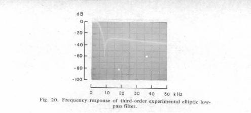
A monolithic implementation of this version of an elliptic filter has been integrated [ 171 and is shown in Fig. 19 using standard MOS technology. The filter was designed for an elliptic lowpass response with 0.1-dB passband ripple, a cut- off frequency of 3400 Hz, and a transmission zero at 8.8 kHz when clocked at 128 kHz. Again, the measured performance shown in Fig. 20 agrees very closely with the design goals as summarized in Table IV.
D. Bandpass Filters
The technique of simulating passive RLC ladders which was used to implement the low-pass filters in the previous section is directly applicable to the design of bandpass filters. An im- portant advantage of these filters is that because of their low sensitivity to component values it is possible to attain rela- tively high values of Q (up to -100) with a high degree of precision.
The bandpass design is based on the use of the standard low- pass to bandpass transformation [ 121 which involves replacing each capacitor and inductor in a normalized low-pass circuit

BRODERSEN et al . : MOS SWITCHED-CAPACITOR FILTERS 73
d B
I I I I I I 0 10 20 30 4 0 50 k H z
Fig. 20. Frequency response of third-order experimental elliptic low- pass filter.
(e.g., see Table I) with a parallel LC (tank) circuit and series LC circuit respectively. The values of the inductor and capaci- tor in the tank circuit which replaces a capacitor are
where oo is the center frequency of the desired bandpass filter, Q is the selectivity ( Q = OO/OBW), WBW is the 3-dB bandwidth, and R T the termination resistance.
The LC values of the series circuit which replace an inductor J, are
RTJQ L , =- WO
The passive prototype circuit is then transformed into a switched capacitor circuit following a method similar to that indicated in Fig. 9. An example of the complete procedure is outlined in Fig. 21 which leads to a second-order bandpass filter. In Fig. 21(a) a normalized low-pass filter (wco = 1 rad/s) is shown which is transformed using the low-pass to bandpass transformation into the circuit shown in 21(b). An all-integrator representation of the circuit is given in 21(c) and the switched-capacitor implementation follows in 21(d). The values of the capacitor ratios in Fig. 2 l(d) are found from ( l ) , (21, (4),and Fig. 21(c).
since = 1 F, it has not been included in the above expres- sions. It can be seen from these equations that if the Q is large then the capacitor ratios can also become very large. The size of the ratios can be minimized, however, by requiring that
_ - RT RS
- Q.
TABLE IV MEASURED PERFORMANCE OF A THIRDORDER ELLIPTIC LOW-PASS
SWITCHED-CAPACITOR FILTER
Clock frequency Ripple bandwidth Total passband ripple Minimum stopband rejection RMS output voltage (l-percent THD) RMS noise (300-3 kHz) Dynamic range Power dissipation Filter die area
128 kHz
0.1 dB 30.4 dB 2.6 V
80 rV 90 dB 18 mW
MOO milZ
3400 Hz
This condition also matches the peak gain from the input to the internal node V i with the gain to the output (which is unity) and, therefore, maximizes the dynamic range. The effect of the sampled data time delays (especially the delay through the termination path) on the transfer function of a second-order bandpass filter is the same as already discussed for a low-pass filter. Therefore, the equations which describe the modification of the capacitor ratios (which retain the same Q and center frequency for the switched capacitor band- pass filter as the prototype LC filter) are the same as those given in (19) a n d , (20). For this to be true, however, the RT/Rs ratio must be set by the condition given (27) and the switches phased as shown in Fig. 7.
Even after minimizing the capacitor ratios, the ratios can be very large for high-Q filters. It is possible, however, t o de- crease the size of the ratios by increasing the sensitivity of the filter. This is accomplished by using the switch phasing for the integrators which was described earlier that gives a fuZZ clock cycle of delay and thus yields an integrator which has an additional phase shift of exp (-jwTc/2) (see (8)). This pre- cisely defined amount of extra phase shift results in a pole movement which increases the Q of the filter (and also in- creases the sensitivity).
As in the case of the low-pass filter shown in Fig. 1 1, single op amp bandpass filters can be implemented which make use of the equivalence between a lossy integrator and an RC circuit. These single op amp structures are essentially switched capaci- tor versions of the infiitegain multiple-feedback bandpass circuits of active-filter theory [ 131.
The implementation of higher order bandpass filters is a straightforward extension of the procedure outlined in Fig. 21. As in the case of the high-order low-pass filters the modi- fications to the capacitor ratios which compensate for sampled data effects in the second-order filters (equations (19) and (20)) are usually not necessary in the high-order bandpass circuits.

74 PROCEEDINGS OF THE IEEE, VOL. 67, NO. 1, JANUARY 1979
Fig. 21. (a) Normalized single-pole low-pass fdter. (b) Bandpass trans- formed low-pass fdter. (c) Integrator realization of bandpass fdter. (d) Switched-capacitor implementation of bandpass filter.
E. Other Filter Organizations The implementation of high-pass and band-reject filters can
also be performed by use of the appropriate transformation on a low-pass LC circuit and then developing the switched capaci- tor realization by the use of the switched-capacitor integrators.
Of course, as mentioned earlier there are many other pos- sible switched-capacitor filteri that are based on active-filter circuits that are consistent with the limitations of the MOS implementation.
There are also switched-capacitor filter organizations which are not based on standard active filters [ 181 -[ 201. One ex- ample is the filter which was shown in Fig. 2. Another is the N-path circuit which uses modulation techniques to translate a very-narrow-low-pass characteristic up to a center frequency which is controlled by the clock rate of the switches [ 201. In this way extremely narrow bandpass and b&d elimination filters can be realized and in fact Q’s in excess of 1000 are readily achievable.
IV. CONCLUSIONS Design considerations for MOS switched-capacitor filters
have been described. The major advantage of this approach is that a broad range of monolithic MOS filters can be realized which are insensitive- to component variations. MOS filters have been designed and tested, and the results confirm the theoretical predictions.
Commercial exploitation of the switched-capacitor filtering technique is proceeding at a rapid pace. The first areas for ap- plication of the technique has been in special-purpose fre- quency selective filters for telecommunications applications,
and in telephone applications in particular. It appears likely that the technique will also be used in monolithic program- mable filters for general-purpose applications.
REFERENCES F. L. J . Sangster, “The bucket brigade delay line, a shift register for analogue signals,” Philips Tech. Rev., vol. 31, pp. 97-110, 1969. D. D. Buss, D. R. Collins, W. H. Bailey, and C. R. Reeves, “Trans- versal filtering using charge transfer devices,” IEEE J. Solidstare
W. Kuntz, “A new sample and hold device and its application t o Circuits, vol. SC-8, pp. 138-146, Apr. 1973.
the realization of digital filters,” Proc. ZEEE, pp. 2092-2093, Nov. 1968. I . A. Young, D. A. Hodges, and P. R. Gray, “Analog MOS sampled- data recursive filters,” in Int. SolidState Circuits Conf. Dig. of
D. L. Fried, “Analog sampled-data filters,” ZEEE J. Solid-state Tech. Papers, pp. 156-157, 1977.
Circuits (Corresp.), SC-7, pp. 302-304, Aug. 1972. B. J. Hosticka, R. W. Brodersen, and P. R. Gray, “MOS sampled data recursive filters using state variable techniques,” in hoc. Znt. Symp. Circuits and Syst., Phoenix, AZ, pp. 525-529, Apr. 1977. J. T. Caves et al., “Sampled analog frttering using switched ca- pacitors as resistor equivalents,” IEEE J. SolidState Circuits, vol. 6,SC-12, pp. 592-599, Dec. 1977. J . L. McCreary and P. R. Gray, “All-MOS charge redistribution analog-to-digital conversion techniques-Part I,” ZEEE 1. Solid- State Circuits,vol. SC-10, pp. 371-379, Dec. 1975. D. Senderowicz, D. A. Hodges, and P. R. Gray, “A high per- formance NMOS operational amplifier,” ZEEE J. SolidState Circuits, Dec. 1978. L. T. Bruton, “Low sensitivity digital ladder filters,” IEEE Trans. Circuitsand Syst., vol. CAS-22, pp. 168-176,Mar. 1975. G. M. Jacobs, D. J. Allstot, R. W. Brodersen, and P. R. Gray, “Design techniques for MOS switched capacitor ladder filters,” ZEEE Trans. Circuirs and Syst., Dec. 1978. See also Proc. Int. Symp. Circuits and Syst., New York, May 1978.
Wiley, 1957. E. A. Guillemin, Synthesis of Pasn’ve Networks. New York:

PROCEEDINGS O F THE IEEE, VOL. 67, NO. 1, JANUARY 1979
[ 131 J. G. Graeme, G. E. Tobey, and L. P. Huelsman, Operational Amplifier Design and Application. New York: McGraw-Hill,
[ 141 B. J . Hosticka, R. W. Brodersen, and P. R. Gray, “MOS sampled 1971.
data recursive filters using switched capacitor integrators,” ZEEE
[ 151 H. J. Orchard, “Inductorless filters,” Elecfron. Lett . , vol. 2, pp. J. SolidState Circuits, vol. SC-12, pp. 600-608, Dec. 1977.
224-225, June 1966. [ 161 F. E. J . Girling and E. F. Good, “The leadfrog or active ladder
synthesis,” Wireless World, pp. 341-345, July 1970. [ 171 D. J. Allstot, R. W. Brodemn, and P. R. Gray, “MOS switched
capacitor ladder filters,” ZEEE J. SolidSrate Circuirs, Dec. 1978. See also Int. Solid-State Circuits Conf. Tech. Dig., San Francisco, CA, pp. 82-83, Feb. 1978.
75
[18] A. Fettweis, “Steady state analysis of circuits containing a
CT-6, pp. 252-260, Sept. 1959. periodically operated switch,” IRE Trans. Circuit Theory, vol.
[ 191 J. McKinney and C. Halijak, “The periodically reverse-switched capacitor,” ZEEE Trans. Circuit Theory, vol. CT-15, pp. 288- 290,1968.
[20] L. E. Franks and I. W. Sandberg, “An alternative approach to the realization of network transfer functions: the N-path filter,” BellSyst. Tech.J.,pp. 1321-1350,Sept. 1960.
[ 2 1 ] P. R. Gray, D. Senderowicz, H. Ohara, and B. W. Warren, “A single-chip NMOS dual channel filter for PCM telephony appli- cations,” in Dig. Tech. Papers, Inr. Solid-State Circuits Conf., Philadelphia, PA., Feb., 1979.:
Crystal, Ceramic, and Mechanical Filters in Japan MORIO ONOE, SENIOR MEMBER, IEEE
Invited Paper
Abstmct-In Japan, there has been considerable activity in the research and manufacturing of quartz crystal filters, ceramic filters and mechan- ical filtem This paper reviews =me of these contributions. An emphasis is placed on filters actually used First multiple-mode resonators are reviewed; this concept having had profound effects on dl types of filters. Qurrtz-crystal filters as w l as other crysta l filters are discussed. Then follow reviews on ceramic and mechanical filters
M I. INTRODUCTION
ECHANICAL resonators have higher Q and stability than do electrical resonant circuits of comparable size. They are also suitable for mass production. Hence in
many cases, more selective, more stable, smaller and more economical filters can be obtained by the use of mechanical resonators. In Japan, there has been a great deal of activity in research and development of crystal, mechanical, ceramic and surface-acoustic-wave (SAW) filters, which are generally called electromechanical (EM) filters. Most of this work, however, has been published only in Japanese and consequently it is little known outside of our country. Hence it would be ben- eficial for readers in English speaking countries to undertake such a review which includes some historical background.
Our usual channels of publication are the Journal and the Transactions of the Institute of Electronics and Communica- tion Engineers of Japan (Translated by Scripta Publishing Company as Electronics and Communication in Japan). Many other papers are presented at monthly meetings of technical groups on Components and Materials, Ultrasonics, Circuits and Systems, etc. as well as at national conventions in the Spring and the Fall.
Furthermore, the activity in EM filters has been effectively suported by several committees who have encouraged active interaction among people of different disciplines from materials t o final applications. The broad spectrum of people and their
Manuscript received August 7, 1978; revised September 29, 1978. The author is with the Institute of Industrial Science, University of
Tokyo, 7-22-1 Roppongi, Tokyo, 106 Japan.
interests enable us to treat a problem from many facets. For example, when monolithic filters vibrating in trapped energy mode were conceived, we were not limited to quartz-crystal filters. We also studied an application to ceramic filters, which resulted a monthly production of a few million ceramic mono- lithic filters.
Among others, the following two permanent committees are notable in terms of their contributions to the development of EM filters.
The Barium Titanate Application Research Committee or the Study Group on Applied Ferroelectrics (The first president: Professor K. Abe and the second president: Professor T. Tanaka) contributed much to the development of ceramic materials and ceramic filters. The group publishes an annual report of papers presented at its regular monthly meetings and also sponsors the Annual Meeting on Ferroelectric Materials and Their Applications [ 1 1.
The Committee on Electromechanical Functional Devices covers EM filters as well as delay lines and oscillators and has published a comprehensive textbook on these subjects [2]. Besides its regular monthly meetings, it sponsors an annual EM Symposium [ 31.
There were also special committees for intensive studies of the following topics under the governmental grant in aid for scientific research:
Multiple-mode piezoelectic vibrators and their applications, 1969-1971 (Chairman: M. Onoe) [3] ;
Piezoelectric materials with high electromechanical coupling and their applications, 1972-1 975 (Chairman: M. Onoe)
Applications of surface acoustic waves to communication, 1975-1976 (Chairman: Professor M. Shibayama, Tohoku University) [ 41 .
I31 ;
No review of EM filters would be complete without covering materials, vibration theory, experimental techniques to observe modes of vibration, filter design, manufacturing, measurement,
0018-9219/79/0100-0075$00.75 0 1979 IEEE