mos-bounded diodes for on-chip esd protection in deep
TRANSCRIPT

IEICE TRANS. ELECTRON., VOL.E88–C, NO.3 MARCH 2005429
PAPER
MOS-Bounded Diodes for On-Chip ESD Protection in DeepSubmicron CMOS Process
Ming-Dou KER†a), Kun-Hsien LIN†, and Che-Hao CHUANG††, Nonmembers
SUMMARY New diode structures without the field-oxide boundaryacross the p/n junction for ESD protection are proposed. A NMOS (PMOS)is especially inserted into the diode structure to form the NMOS-bounded(PMOS-bounded) diode, which is used to block the field oxide isolationacross the p/n junction in the diode structure. The proposed N(P)MOS-bounded diodes can provide more efficient ESD protection to the internalcircuits, as compared to the other diode structures. The N(P)MOS-boundeddiodes can be used in the I/O ESD protection circuits, power-rail ESDclamp circuits, and the ESD conduction cells between the separated powerlines. From the experimental results, the human-body-model ESD levelof ESD protection circuit with the proposed N(P)MOS-bounded diodes isgreater than 8 kV in a 0.35-µm CMOS process.key words: electrostatic discharge (ESD), diode, poly-bounded diode,MOS-bounded diode, ESD protection
1. Introduction
To scale down device dimension, the shallower junctiondepth, much thinner gate oxide, salicided (self-aligned sili-cide) process, and LDD (lightly-doped drain) structure hadbeen widely used in deep submicron CMOS technology.But, those advanced process technologies result in theCMOS integrated circuits more susceptible to electrostaticdischarge (ESD) damage [1]–[3]. To sustain a reasonableESD stress (typically, ±2 kV in the human-body-model ESDevent [4]) for safe mass production, on-chip ESD protectioncircuits have to be added into the IC products. The typ-ical ESD protection circuit with double diodes for a padis shown in Fig. 1 [5]. To avoid unexpected ESD damagein the internal circuits of CMOS ICs, the power-rail ESDclamp circuit must be placed between the VDD and VSSpower lines [6]. The ESD current at the input pad under thepositive-to-VSS (PS-mode) ESD stress condition can be dis-charged through the forward-biased P-type diode (Dp) andthe VDD-to-VSS ESD clamp circuit to ground. However, ifthe turn-on resistance of the power-rail ESD clamp circuit istoo high or the device dimension of P-type diode is drawntoo small, the overshooting voltage on the input pad couldbe so high to cause the reverse-biased junction breakdownon the N-type diode (Dn). Therefore, the diodes under both
Manuscript received July 20, 2004.Manuscript revised November 3, 2004.†The authors are with Nanoelectronics and Gigascale Systems
Laboratory, Institute of Electronics, National Chiao-Tung Univer-sity, 1001 Ta-Hsueh Road, Hsinchu, Taiwan.††The author is with ESD and Product Engineering Department,
SoC Technology Center, Industrial Technology Research Institute,Taiwan.
a) E-mail: [email protected]: 10.1093/ietele/e88–c.3.429
Fig. 1 The typical ESD protection design with double diodes for an inputpad.
Fig. 2 The pull-down weakest point at the boundary between the field-oxide shallow-trench isolation (STI) and the diffusion edge of the diodestructure [7].
forward-biased and reverse-biased stress conditions are im-portant concerns of providing efficient ESD protection to theinternal circuits.
When the diodes are stressed by the ESD pulse underthe reverse-biased stress conditions, which are the positive-to-VSS (PS-mode) ESD stress for N-type diode and thenegative-to-VDD (ND-mode) ESD stress for P-type diode,the diffusion boundary to the field-oxide isolation is easilydamaged by ESD to cause a very low ESD robustness [7].The weakest point at the boundary between the field-oxideshallow-trench isolation (STI) and the diffusion edge of thediode structure is illustrated in Fig. 2, where the field-oxideregion near to the P+ diffusion has a pull-down structure.When the p/n junction is reverse biased during ESD stress,the breakdown point is located at the boundary between theP+ diffusion and field-oxide region. Due to the limited areaof the boundary for heat dissipation, this pull-down struc-ture on the field-oxide boundary often causes the P+ diffu-sion having a lower ESD robustness on its diffusion edge.If the CMOS process has the silicided diffusion, the sili-cided layer covered on the P+ diffusion causes a bend-down
Copyright c© 2005 The Institute of Electronics, Information and Communication Engineers

430IEICE TRANS. ELECTRON., VOL.E88–C, NO.3 MARCH 2005
corner at the boundary between the P+ diffusion and field-oxide region [7], [8]. This bend-down corner further causesthe diode being more easily damaged by ESD. Thus, theESD protection circuits formed by double diodes often havelower ESD robustness in the reverse-biased ESD-stress con-ditions (PS-mode and ND-mode ESD stresses), even if thediodes have been drawn with larger silicon area.
In this paper, new diode structures, called as NMOS-bounded diode and PMOS-bounded diode, are proposedto significantly improve ESD robustness of CMOS ICs indeep-submicron CMOS processes [9], [10]. With the newproposed diode structures, the on-chip ESD protection cir-cuits for input, output, and power pads have been designedand practically verified in a 0.35-µm CMOS process.
2. Diode Structures
2.1 Normal Diodes
The cross-sectional view of the normal N-type diode real-ized in a deep submicron CMOS process is shown in Fig. 3.For the normal N-type diode, N+ diffusion (as the cathode)is placed in a P-well in P-substrate to form the p/n junctionof the diode. The anode of such an N-type diode is con-nected out by the P+ diffusion in the P-well (or p-substrate).Between the P+ and N+ diffusions, there is the field-oxideregion to isolate these two diffusions. For the normal P-typediode, P+ diffusion (as the anode) is placed in an N-well toform the p/n junction of the diode. The cathode of such aP-type diode is connected out by the N+ diffusion in the N-well. Between the P+ and N+ diffusions, there is the field-oxide region to isolate these two diffusions.
2.2 Poly-Bounded Diodes
To overcome the weakest ESD-damaged location at the p/njunction diffusion to the field-oxide boundary, the modi-fied diode structures with dummy gate [7], [11], [12], calledas the poly-bounded N-type (P-type) diodes, had been re-ported. The cross-sectional view of the poly-bounded N-type diode realized in a deep submicron CMOS process isshown in Fig. 4. As comparing to Fig. 3, the field-oxideisolation regions between the P+ and N+ diffusions are re-moved away from the N+ diffusion of the normal N-typediode and replaced by the dummy poly gates. The dummypoly gates are located half on the P-well region and half
Fig. 3 The device cross-sectional view of the normal N-type diode inCMOS process.
on the field-oxide region. Therefore, there is no field-oxideboundary to the N+ diffusion edge of the poly-bounded N-type diode. Without the field-oxide boundary at the p/n junc-tion of the diode, the pull-down and bend-down corner inFig. 2 that causes low ESD robustness can be overcome.
2.3 NMOS-Bounded and PMOS-Bounded Diodes
The layout top views and the device cross-sectional views
Fig. 4 The device cross-sectional view of the poly-bounded N-typediode in CMOS process.
(a)
(b)
Fig. 5 The layout top views and the device cross-sectional views of (a)the NMOS-bounded diode, and (b) the PMOS-bounded diode, in CMOSprocess.
KER et al.: MOS-BOUNDED DIODES FOR ON-CHIP ESD PROTECTION IN DEEP SUBMICRON CMOS PROCESS431
of the new proposed NMOS-bounded diode and PMOS-bounded diode are shown in Figs. 5(a) and 5(b), respec-tively, where the corresponding symbols are also shown inFigs. 5(a) and 5(b). These symbols will be used to draw theon-chip ESD protection circuits in Sect. 4. The N(P)MOS-bounded diode has an N(P)MOS structure inserted in thediode structure. The NMOS-bounded diode in Fig. 5(a) hasa cathode of N+ diffusion, which does not directly touchthe P+ diffusion in the diode structure. The diode anodeof P+ diffusion directly touches another N+ diffusion inthe NMOS-bounded diode, but this N+ diffusion is floatingin the device structure. The anode of the PMOS-boundeddiode in Fig. 5(b) is the P+ diffusion in the center regionof device structure, which does not directly touch the N+diffusion. The cathode of PMOS-bounded diode is the N+diffusion, which directly touches another P+ diffusion in thediode structure, but this P+ diffusion is floating in the de-vice structure. Therefore, silicide-blocking mask is usedto block the silicided layer covered on the anode P+ dif-fusion/floating N+ diffusion (cathode N+ diffusion/floatingP+ diffusion) of the N(P)MOS-bounded diode in the sili-cided or salicided CMOS processes. In this N(P)MOS-bounded diode, the poly gate is fully covered by the N+(P+)implantation, therefore the gate function can be successfullyformed on the NMOS (PMOS) channel. The poly gate inthe layout top view has a close-loop ring to block the field-oxide boundary from the cathode N+ diffusion (anode P+diffusion) of the N(P)MOS-bounded diode structure.
3. Experimental Results
The new proposed N(P)MOS-bounded diodes, the tradi-tional normal diodes, and the poly-bounded diodes hadbeen fabricated in a 0.35-µm CMOS process without sili-cided diffusion. In this study, the gate length of N(P)MOS-Bounded Diodes is 0.35 µm and the gate oxide thicknessis 70 Å. The dc I-V characteristics of the diodes are mea-sured by HP4155. To investigate the turn-on behavior ofthe diodes during high ESD current stress, transmission linepulse (TLP) generator with the pulse width of 100 ns isused to measure the second breakdown current (It2) [13].The ESD protection circuits with diodes under four differ-ent stress modes which include PS-mode (positive-to-VSS),ND-mode (negative-to-VDD), NS-mode (negative-to-VSS),and PD-mode (positive-to-VDD) are measured by the Zap-Master ESD tester to verify their ESD robustness. The fail-ure criterion is defined at the leakage current greater than1 µA under 3.3-V reverse bias.
3.1 DC I-V Characteristics
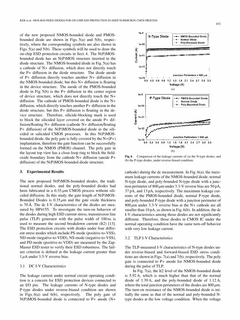
The leakage current under normal circuit operating condi-tion is a concern for ESD protection devices connected toan I/O pin. The leakage currents of N-type diodes andP-type diodes under reverse-biased condition are shownin Figs. 6(a) and 6(b), respectively. The poly gate ofN(P)MOS-bounded diode is connected to P+ anode (N+
(a)
(b)
Fig. 6 Comparison of the leakage currents of (a) the N-type diodes, and(b) the P-type diodes, under reverse-biased condition.
cathode) during the dc measurement. In Fig. 6(a), the maxi-mum leakage currents of the NMOS-bounded diode, normalN-type diode, and poly-bounded N-type diode with a junc-tion perimeter of 800µm under 3.3-V reverse bias are 50 pA,37 pA, and 13 pA, respectively. The maximum leakage cur-rents of the PMOS-bounded diode, normal P-type diode,and poly-bounded P-type diode with a junction perimeter of800 µm under 3.3-V reverse bias at the N+ cathode are allsmaller than 10 pA, as shown in Fig. 6(b). In addition, the dcI-V characteristics among those diodes are not significantlydifferent. Therefore, those diodes in CMOS IC under thenormal operating condition have the same turn-off behaviorwith very low leakage current.
3.2 TLP I-V Characteristics
The TLP-measured I-V characteristics of N-type diodes un-der reverse-biased and forward-biased ESD stress condi-tions are shown in Figs. 7(a) and 7(b), respectively. The polygate is connected to P+ anode for NMOS-bounded diodeduring the pulse of TLP.
In Fig. 7(a), the It2 level of the NMOS-bounded diodeis 5.92 A, which is much higher than that of the normaldiode of 1.39 A, and the poly-bounded diode of 1.12 A,where the total junction perimeters of the diodes are 800 µm.The turn-on resistance of the NMOS-bounded diode is ini-tially the same as that of the normal and poly-bounded N-type diodes at the low voltage condition. When the voltage

432IEICE TRANS. ELECTRON., VOL.E88–C, NO.3 MARCH 2005
(a)
(b)
Fig. 7 The TLP-measured I-V characteristics of N-type diodes (a) underPS-mode stress condition and (b) under NS-mode stress condition.
is more increased, the turn-on resistance of NMOS-boundeddiode is reduced significantly, as shown in Fig. 7(a). TheESD current flows through the diode path of the NMOS-bounded diode, when the diode is stressed with low-voltagelevel ESD stress. But, under the high-voltage ESD stresscondition, the parasitic lateral n-p-n bipolar transistor in theNMOS-bounded diode structure is turned on to dischargeESD current. The gate-grounded NMOS device often suf-fers the non-uniform turn-on issue caused by the snapbackeffect of the parasitic lateral bipolar transistor, especiallywhen the device is drawn with a large device width [14].Because the ESD current flows through the diode path of theNMOS-bounded diode under low-voltage level ESD stress,the non-uniform turn-on issue of the parasitic lateral bipolartransistor in NMOS-bounded diode can be avoided. In addi-tion, the small turn-on resistance and low holding voltage ofparasitic lateral n-p-n bipolar transistor enable the NMOS-bounded diode to sustain much higher ESD level. Therefore,the better ESD protection capability can be achieved by theNMOS-bounded diode than that of the normal and poly-bounded N-type diodes under reverse-biased ESD stresscondition.
In Fig. 7(b), the It2 levels of three kinds of diodes un-der forward-biased ESD stress condition are nearly 5 A withthe total diode junction perimeter of 400µm. The turn-onresistance of the NMOS-bounded diode has no significantdifference as compared to that of other diode structures un-
Fig. 8 The clamped voltage waveforms by different N-type diodes underPS-mode stress with a 50-V TLP pulse.
der forward-biased ESD stress. High ESD robustness can beachieved by the N-type diodes under forward-biased condi-tion.
3.3 Turn-On Verification
A voltage pulse generated from the TLP system with a pulseheight of 50 V and a rise time of ∼10 ns is used to simulatethe rising edge of ESD pulse. Such a voltage pulse is appliedto the N-type diodes under reverse-biased condition to verifythe turn-on behavior of the diodes in time domain. The volt-age waveforms clamped by different N-type diodes underthe stress of a 50-V TLP pulse are shown in Fig. 8, wherethe clamped voltage level of the diodes has the sequenceof: poly-bounded diode (22 V) > normal diode (18.5 V) >NMOS-bounded diode (14 V). The NMOS-bounded diodehas the lowest clamped voltage of 14 V. The measured re-sult is consistent with the TLP-measured I-V characteristicsshown in Fig. 7(a). Therefore, the NMOS-bounded diodewith a lower clamped voltage can provide more efficientESD protection to the internal circuits.
3.4 ESD Robustness
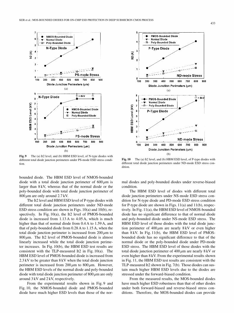
The It2 level and human body model (HBM) ESD level ofN-type diodes with different total diode junction perimetersunder PS-mode ESD stress condition are shown in Figs. 9(a)and 9(b), respectively. In Fig. 9(a), the NMOS-boundeddiode has much higher It2 level than that of the normaldiode or the poly-bounded diode. The It2 level of NMOS-bounded diode is almost linearly increased while the to-tal diode junction perimeter increases. The It2 level ofNMOS-bounded diode is increased from 1.79 A to 5.92 Awhen the total diode junction perimeter is increased from200 µm to 800 µm, whereas that of the normal diode orthe poly-bounded diode with total diode junction perime-ter of 800 µm is only around 1.4 A. In Fig. 9(b), the HBMESD test results are consistent with the TLP-measured It2in Fig. 9(a). The NMOS-bounded diode has much higherHBM ESD level than that of the normal diode or the poly-
KER et al.: MOS-BOUNDED DIODES FOR ON-CHIP ESD PROTECTION IN DEEP SUBMICRON CMOS PROCESS433
(a)
(b)
Fig. 9 The (a) It2 level, and (b) HBM ESD level, of N-type diodes withdifferent total diode junction perimeters under PS-mode ESD stress condi-tion.
bounded diode. The HBM ESD level of NMOS-boundeddiode with a total diode junction perimeter of 600 µm islarger than 8 kV, whereas that of the normal diode or thepoly-bounded diode with total diode junction perimeter of800 µm are only around 2.7 kV.
The It2 level and HBM ESD level of P-type diodes withdifferent total diode junction perimeters under ND-modeESD stress condition are shown in Figs. 10(a) and 10(b), re-spectively. In Fig. 10(a), the It2 level of PMOS-boundeddiode is increased from 1.13 A to 4.05 A, which is muchhigher than that of normal diode from 0.4 A to 1.59 A, andthat of poly-bounded diode from 0.28 A to 1.15 A, when thetotal diode junction perimeter is increased from 200 µm to800 µm. The It2 level of PMOS-bounded diode is almostlinearly increased while the total diode junction perime-ter increases. In Fig. 10(b), the HBM ESD test results areconsistent with the TLP-measured It2 in Fig. 10(a). TheHBM ESD level of PMOS-bounded diode is increased from2.3 kV to be greater than 8 kV when the total diode junctionperimeter is increased from 200 µm to 800 µm. However,the HBM ESD levels of the normal diode and poly-boundeddiode with total diode junction perimeter of 800 µm are onlyaround 3 kV and 2 kV, respectively.
From the experimental results shown in Fig. 9 andFig. 10, the NMOS-bounded diode and PMOS-boundeddiode have much higher ESD levels than those of the nor-
(a)
(b)
Fig. 10 The (a) It2 level, and (b) HBM ESD level, of P-type diodes withdifferent total diode junction perimeters under ND-mode ESD stress con-dition.
mal diodes and poly-bounded diodes under reverse-biasedcondition.
The HBM ESD level of diodes with different totaldiode junction perimeters under NS-mode ESD stress con-dition for N-type diode and PD-mode ESD stress conditionfor P-type diode are shown in Figs. 11(a) and 11(b), respec-tively. In Fig. 11(a), the HBM ESD level of NMOS-boundeddiode has no significant difference to that of normal diodeand poly-bounded diode under NS-mode ESD stress. TheHBM ESD level of those diodes with the total diode junc-tion perimeter of 400 µm are nearly 8 kV or even higherthan 8 kV. In Fig. 11(b), the HBM ESD level of PMOS-bounded diode has no significant difference to that of thenormal diode or the poly-bounded diode under PD-modeESD stress. The HBM ESD level of those diodes with thetotal diode junction perimeter of 400 µm are nearly 8 kV oreven higher than 8 kV. From the experimental results shownin Fig. 11, the HBM ESD test results are consistent with theTLP-measured It2 shown in Fig. 7(b). Those diodes can sus-tain much higher HBM ESD levels due to the diodes arestressed under the forward-biased condition.
From the measured results, the MOS-bounded diodeshave much higher ESD robustness than that of other diodesunder both forward-biased and reverse-biased stress con-ditions. Therefore, the MOS-bounded diodes can provide
434IEICE TRANS. ELECTRON., VOL.E88–C, NO.3 MARCH 2005
(a)
(b)
Fig. 11 The HBM ESD levels of diodes with different total diode junc-tion perimeters under (a) NS-mode ESD stress condition for N-type diodes,and (b) PD-mode ESD stress condition for P-type diodes.
more effective ESD protection to the internal circuits in theESD protection scheme shown in Fig. 1.
4. Applications for On-Chip ESD Protection
With the new proposed NMOS-bounded or PMOS-boundeddiodes, some new on-chip ESD protection circuits have beendesigned to achieve higher ESD robustness and better pro-tection capability for protecting the internal circuits [10].
4.1 ESD Protection Circuits for I/O Pad
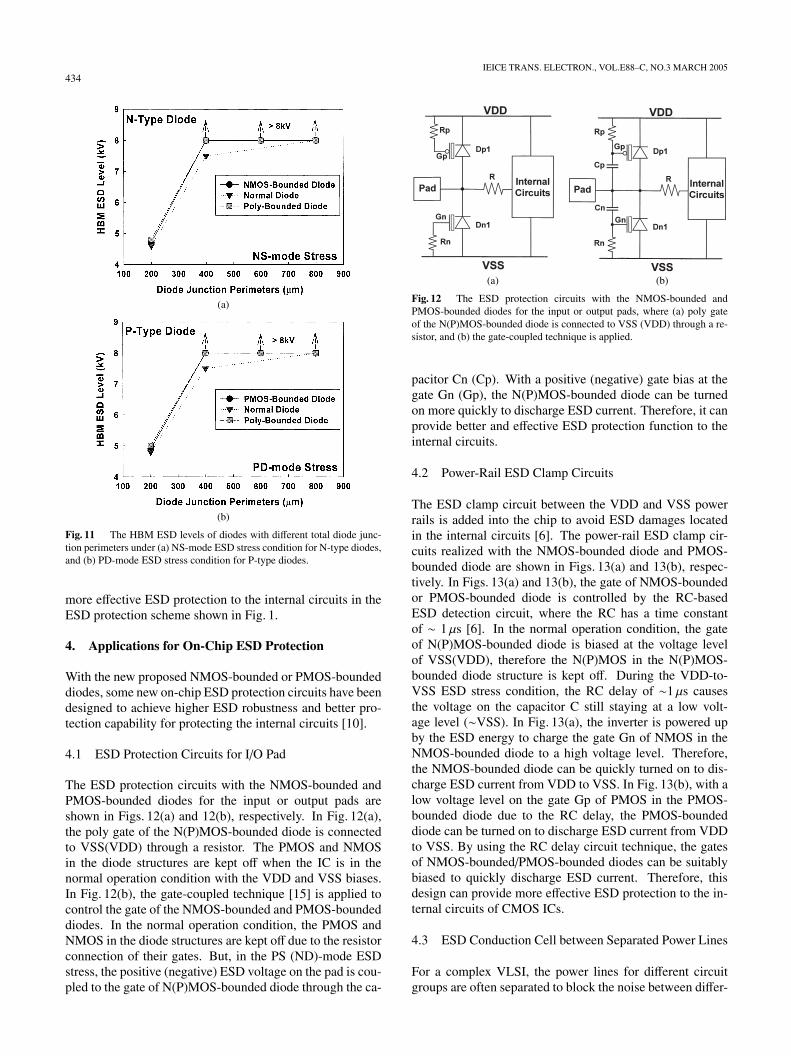
The ESD protection circuits with the NMOS-bounded andPMOS-bounded diodes for the input or output pads areshown in Figs. 12(a) and 12(b), respectively. In Fig. 12(a),the poly gate of the N(P)MOS-bounded diode is connectedto VSS(VDD) through a resistor. The PMOS and NMOSin the diode structures are kept off when the IC is in thenormal operation condition with the VDD and VSS biases.In Fig. 12(b), the gate-coupled technique [15] is applied tocontrol the gate of the NMOS-bounded and PMOS-boundeddiodes. In the normal operation condition, the PMOS andNMOS in the diode structures are kept off due to the resistorconnection of their gates. But, in the PS (ND)-mode ESDstress, the positive (negative) ESD voltage on the pad is cou-pled to the gate of N(P)MOS-bounded diode through the ca-
(a) (b)
Fig. 12 The ESD protection circuits with the NMOS-bounded andPMOS-bounded diodes for the input or output pads, where (a) poly gateof the N(P)MOS-bounded diode is connected to VSS (VDD) through a re-sistor, and (b) the gate-coupled technique is applied.
pacitor Cn (Cp). With a positive (negative) gate bias at thegate Gn (Gp), the N(P)MOS-bounded diode can be turnedon more quickly to discharge ESD current. Therefore, it canprovide better and effective ESD protection function to theinternal circuits.
4.2 Power-Rail ESD Clamp Circuits
The ESD clamp circuit between the VDD and VSS powerrails is added into the chip to avoid ESD damages locatedin the internal circuits [6]. The power-rail ESD clamp cir-cuits realized with the NMOS-bounded diode and PMOS-bounded diode are shown in Figs. 13(a) and 13(b), respec-tively. In Figs. 13(a) and 13(b), the gate of NMOS-boundedor PMOS-bounded diode is controlled by the RC-basedESD detection circuit, where the RC has a time constantof ∼ 1 µs [6]. In the normal operation condition, the gateof N(P)MOS-bounded diode is biased at the voltage levelof VSS(VDD), therefore the N(P)MOS in the N(P)MOS-bounded diode structure is kept off. During the VDD-to-VSS ESD stress condition, the RC delay of ∼1 µs causesthe voltage on the capacitor C still staying at a low volt-age level (∼VSS). In Fig. 13(a), the inverter is powered upby the ESD energy to charge the gate Gn of NMOS in theNMOS-bounded diode to a high voltage level. Therefore,the NMOS-bounded diode can be quickly turned on to dis-charge ESD current from VDD to VSS. In Fig. 13(b), with alow voltage level on the gate Gp of PMOS in the PMOS-bounded diode due to the RC delay, the PMOS-boundeddiode can be turned on to discharge ESD current from VDDto VSS. By using the RC delay circuit technique, the gatesof NMOS-bounded/PMOS-bounded diodes can be suitablybiased to quickly discharge ESD current. Therefore, thisdesign can provide more effective ESD protection to the in-ternal circuits of CMOS ICs.
4.3 ESD Conduction Cell between Separated Power Lines
For a complex VLSI, the power lines for different circuitgroups are often separated to block the noise between differ-

KER et al.: MOS-BOUNDED DIODES FOR ON-CHIP ESD PROTECTION IN DEEP SUBMICRON CMOS PROCESS435
(a) (b)
Fig. 13 The power-rail ESD protection circuits realized by (a) theNMOS-bounded diode, and (b) the PMOS-bounded diode, with RC-basedESD detection circuit.
Fig. 14 The ESD protection networks realized with NMOS-bounded andPMOS-bounded diodes between the separated power rails. The stackedNMOS-bounded and PMOS-bounded diodes in back-to-back configurationare used to connect the different power lines.
ent circuit groups. But, an IC with the separated power linesoften has some unexpected ESD damages located on the in-terface circuits between the circuit groups [16]. To avoid theESD damage on the interface or internal circuits, the ESD-conduction cell is added between the separated power lines[17]. The NMOS-bounded and PMOS-bounded diodes instacked configuration can be placed between the separatedpower rails to provide the ESD current discharging paths.In Fig. 14, the stacked PMOS-bounded (NMOS-bounded)diodes in back-to-back configuration are used to connectVDD1 (VSS1) and VDD2 (VSS2) power lines to provideESD current discharging paths. The PMOS-bounded diodesforward-stacked (backward-stacked) from VDD1 to VDD2have gates controlled by RC-based ESD detection circuit ofcircuit 1 (circuit 2) to quickly discharge ESD current. Inaddition, the gate of each NMOS-bounded diode is con-nected to its cathode of each NMOS-bounded diode. Thepower-rail ESD clamp circuits in Fig. 14 can be realized bythose circuits shown in Fig. 13. By using these ESD protec-tion networks, the interface circuits and internal circuits ofCMOS IC can be fully protected against ESD damage.
5. Conclusion
DC characteristics, TLP characteristics, turn-on verification,and ESD robustness of N(P)MOS-bounded diodes for ESD
protection in a 0.35-µm CMOS process have been inves-tigated and compared to that of normal N(P)-type diodeand poly-bounded N(P)-type diode. With the new proposedMOS-bounded diode structure, the parasitic lateral bipo-lar transistor in the MOS-bounded diode has shown with asmall turn-on resistance and a low holding voltage to sustainmuch higher ESD level. The proposed N(P)MOS-boundeddiodes can sustain the HBM ESD stress of > 8 kV withthe total diode junction perimeter of 800 µm in a 0.35-µmCMOS process in all modes of ESD stresses. The experi-mental results have confirmed that the new proposed diodestructures with higher HBM ESD robustness are more suit-able for on-chip ESD protection design than the other diodestructures in deep-submicron CMOS processes.
References
[1] A. Amerasekera and C. Duvvury, “The impact of technology scalingon ESD robustness and protection circuit design,” Proc. EOS/ESDSymp., pp.237–245, 1994.
[2] C. Jiang, E. Nowak, and M. Manley, “Process and design for ESDrobustness in deep submicron CMOS technology,” Proc. IEEE Int.Reliability Physics Symp., pp.233–236, 1996.
[3] G. Notermans, A. Heringa, M. Van Dort, S. Jansen, and F. Kuper,“The effect of silicide on ESD performance,” Proc. IEEE Int. Relia-bility Physics Symp., pp.154–158, 1999.
[4] ESD Association Standard Test Method ESD STM5.1-1998, forElectrostatic Discharge Sensitivity Testing—Human Body Model(HBM)—Component Level, 1998.
[5] J. Bernier, G. Croft, and W. Young, “A process independent ESD de-sign methodology,” Proc. IEEE Int. Symp. on Circuits and Systems,pp.218–221, 1999.
[6] M.-D. Ker, “Whole-chip ESD protection design with efficient VDD-to-VSS ESD clamp circuits for submicron CMOS VLSI,” IEEETrans. Electron Devices, vol.46, no.1, pp.173–183, 1999.
[7] S. Voldman, S. Geissler, J. Nakos, J. Pekarik, and R. Gauthier,“Semiconductor process and structural optimization of shallowtrench isolation-defined and polysilicon-bound source/drain diodesfor ESD networks,” Proc. EOS/ESD Symp., pp.151–160, 1998.
[8] J.H. Lee, S.H. Park, K.M. Lee, K.S. Youn, Y.J. Park, C.J. Choi,T.Y. Seong, and H.D. Lee, “A study of stress-induced p+/n salicidedjunction leakage failure and optimized process conditions for sub-0.15-µm CMOS technology,” IEEE Trans. Electron Devices, vol.49,no.11, pp.1985–1992, 2002.
[9] M.-D. Ker and C.-H. Chuang, “ESD protection circuits with novelMOS-bounded diode structures,” Proc. IEEE Int. Symp. on Circuitsand Systems, pp.533–536, 2002.
[10] M.-D. Ker, H.-H. Chang, and W.-T Wang, “ESD protection networkswith NMOS-bound or PMOS-bound diode structures in a shallow-trench-isolation (STI) CMOS process,” US patent # 6576958, 2003.
[11] Y. Omura, “A lateral, unidirectional, bipolar-type insulated-gatetransistor—A novel semiconductor device,” Appl. Phys. Lett.,vol.40, no.6, pp.528–529, 1982.
[12] S. Voldman, “Semiconductor diode with silicide films and trenchisolation,” US patent # 5629544, 1997.
[13] T.J. Maloney and N. Khurana, “Transmission line pulsing tech-niques for circuit modeling of ESD phenomena,” Proc. EOS/ESDSymp., pp.49–54, 1985.
[14] T.-Y. Chen and M.-D. Ker, “Analysis on the dependence of layoutparameters on ESD robustness of CMOS devices for manufacturingin deep-submicron CMOS process,” IEEE Trans. Semicond. Manuf.,vol.16, no.3, pp.486–500, 2003.
[15] M.-D. Ker, C.-Y. Wu, T. Cheng, and H.-H. Chang, “Capacitor-couple ESD protection circuit for deep-submicron low-voltage

436IEICE TRANS. ELECTRON., VOL.E88–C, NO.3 MARCH 2005
CMOS ASIC,” IEEE Trans. Very Large Scale Integr. (VLSI) Syst.,vol.4, no.3, pp.307–321, 1996.
[16] M.-D. Ker, C.-Y. Chang, and Y.-S. Chang, “ESD protection design toovercome internal damages on interface circuits of CMOS IC withmultiple separated power pins,” Proc. IEEE Int. ASIC/SOC Conf.,pp.234–238, 2002.
[17] M.-D. Ker, “ESD protection circuit for mixed mode integrated cir-cuits with separated power pins,” US patent # 6075686, 2000.
Ming-Dou Ker received the Ph.D. de-gree from the Institute of Electronics, Na-tional Chiao-Tung University, Hsinchu, Taiwan,R.O.C., in 1993. Now, he is a Professor inthe Department of Electronics, National Chiao-Tung University. In the field of reliability andquality design for CMOS integrated circuits, hehas published over 200 technical papers in in-ternational journals and conferences. He has in-vented over 180 patents on reliability and qual-ity design for integrated circuits, including 83
U.S. patents and 98 R.O.C. patents. Dr. Ker has been a Senior Member ofIEEE, since 1997.
Kun-Hsien Lin received the B.S. de-gree from the Department of Electronics En-gineering and the M.S. degree from the Insti-tute of Electronics, National Chiao-Tung Uni-versity, Hsinchu, Taiwan, in 1996 and 1998, re-spectively. From 2000 to 2001, he was a Prod-uct Engineer in the Taiwan Semiconductor Man-ufacturing Company (TSMC). Currently, he isworking toward the Ph.D. degree at the Instituteof Electronics, National Chiao-Tung University,Taiwan.
Che-Hao Chuang received the B.S. degreefrom the Department of Electrophysics and theM.S. degree from the Institute of Electronics,National Chiao-Tung University, Hsinchu, Tai-wan, in 1999 and 2001, respectively. In 2002,he joined Industrial Technology Research Insti-tute (ITRI), as an I/O Cell Library and ESD Pro-tection Design Engineer. In 2004, he became aSection Manager of the ESD Protection DesignSection.