morphology control of metal oxide nanocrystals
TRANSCRIPT

1
Morphology Control of Metal Oxide Nanocrystals
Yoshitake Masuda National Institute of Advanced Industrial Science and Technology (AIST)
Anagahora, Shimoshidami, Moriyama-ku, Nagoya Japan
1. Introduction
Metal oxides have been widely used in electro devices, optical devices, etc. Recently, liquid phase syntheses of them attract much attention as future technology and novel academic field. Especially, liquid phase syntheses of anisotropic particles or films are expected for next generation metal oxide devices. This section describes liquid phase morphology control of anisotropic metal oxide. They were realized by precise control of nucleation and crystal growth. They showed high performance of solution systems for future metal oxide devices. Liquid phase morphology control of anisotropic metal oxide particles and films would contribute to development of metal oxide science and technology.
2. Morphology control of acicular BaTiO3 particles1
Acicular BaTiO3 particles were developed using solution systems. The morphology of BaC2O4 0.5H2O was controlled to acicular shape. Its phase transition to BaTiO3 was realized by introducing Ti ions from the coprecipitated amorphous phase. Acicular BaTiO3 particles have an aspect ratio as high as 18 and the particle size can be controlled by varying the growth period of BaC2O4 · 0.5H2O which governs the size of BaC2O4 · 0.5H2O particles. Acicular particles of crystalline BaTiO3 can be used for ultra-thin multilayer ceramic capacitors. Multilayer ceramic capacitors (MLCC) are indispensable electronic components for advanced electronic technology2-12, but larger capacity and smaller size are needed for future electronic devices. To meet these needs, BaTiO3 particles were downsized, but ferroelectric ceramics lose their ferroelectricity when their particle size is decreased and lose ferroelectricity entirely at a critical size2-11. This is known as the size effect and it impedes the progress of MLCC, so a novel solution has been eagerly anticipated. Here, we propose MLCC using acicular BaTiO3 particles13. An ultra-thin ferroelectric layer and high capacity can be realized by acicular particles having a high aspect ratio. The short side provides an ultra-thin ferroelectric layer and the large volume caused by the long side avoids the loss of ferroelectricity at the critical size. Anisotropic BaTiO3 particles are thus a candidate for MLCC. BaTiO3 has, however, an isotropic cubic or tetragonal structure, and its morphology is extremely difficult to control due to its isotropic crystal faces. We focused on triclinic BaC2O4 · 0.5H2O which has an anisotropic crystal structure and controlled the morphology of these particles by precisely controlling crystal growth. We also achieved
www.intechopen.com

Nanocrystal
4
phase transition of BaC2O4 · 0.5H2O to crystalline BaTiO3 by introducing Ti ions from the coprecipitated amorphous phase. Having developed several key technologies, we were successfully able to produce anisotropic acicular BaTiO3 particles. Morphology control of BaTiO3 to rod-shape was reported previously. Additionally, metal oxalates (MC2O4) have been used for synthesis of rod-shaped oxides or hydroxides. Y. Hayashi et al. reported preparation of rod-shaped BaTiO3 from rod-shaped TiO2-nH2O and BaCO3 in molten chloride at high temperature14. Li et al. reported preparation of nanoflakes and nanorods of Ni(OH)2, Co(OH)2 and Fe3O4 by hydrothermal conversion at 160 °C for 12 h from MC2O4·2H2O in NaOH solutions15. Sun et al. prepared flowerlike SnC2O4 submicrotubes in ethanol solutions containing SnCl2 and oxalic acid. They were annealed at 500 °C for 2 h in ambient atmosphere to obtain flowerlike SnO2 submicrotubes16. Oxalic acid (252 mg) was dissolved into isopropyl alcohol (4 ml) (Fig. 1)1. Butyl titanate monomer (0.122 ml) was mixed with the oxalic acid solution, and the solution was then mixed with distilled water (100 ml). The pH of the solution was increased to pH = 7 by adding NaOH (1 M) and distilled water, while the volume of the solution was adjusted to 150 ml by these additions. The aqueous solution (50 ml) with barium acetate (39.3 mg) was mixed with the oxalic acid solution. The mixed solution containing barium acetate (0.77 mM), butyl titanate monomer (2 mM) and oxalic acid (10 mM) was kept at room temperature for several hours with no stirring, and the solution gradually became cloudy. Stirring causes the collision of homogeneously nucleated particles and destruction of large grown particles, and so was avoided in this process. The size of the precipitate was easily controlled from nanometer order to micrometer order by changing the growth period. Large particles were grown by immersion for several hours to evaluate the morphology and crystallinity in detail.
Fig. 1. Conceptual process for fabricating acicular BaTiO3 particles. Morphology control of BaC2O4 � 0.5H2O particles and phase transition to BaTiO3. Reprinted with permission from Ref.1, Masuda, Y., Yamada, T. and Koumoto, K., 2008, Cryst. Growth Des., 8, 169. Copyright @American Chemical Society
Oxalate ions (C2O42-) react with barium ions (Ba2+) to form barium oxalate (BaC2O4 · 0.5H2O). BaC2O4 · 0.5H2O is dissolved in weak acetate acid provided by barium acetate ((CH3COO)2Ba), however, it can be deposited at pH 7 which is adjusted by adding NaOH. BaC2O4 · 0.5H2O was thus successfully precipitated from the solution. Acicular particles were homogeneously nucleated and precipitated from the solution. They were on average 23 µm (ranging from 19 to 27 µm) in width and 167 µm (ranging from 144 to 189 µm) in length, giving a high aspect ratio of 7.2 (Fig. 2). They had sharp edges and clear crystal faces, indicating high crystallinity. A gel-like solid was also coprecipitated from the solution as a second phase.
www.intechopen.com

Morphology Control of Metal Oxide Nanocrystals
5
Fig. 2. SEM micrograph and XRD diffraction pattern of acicular BaC2O4 � 0.5H2O particles precipitated from an aqueous solution at pH = 7. XRD diffraction measurement data (first step), XRD pattern calculated from crystal structure data16 (second step) and XRD pattern of JCPDS No. 20-134 (third step) are shown for triclinic BaC2O4 � 0.5H2O. Reprinted with permission from Ref.1, Masuda, Y., Yamada, T. and Koumoto, K., 2008, Cryst. Growth Des., 8, 169. Copyright @American Chemical Society
XRD diffraction patterns for the mixture of acicular particles and gel-like solid showed sharp diffraction peaks of crystalline BaC2O4 · 0.5H2O with no additional phase. Acicular particles were crystalline BaC2O4 · 0.5H2O and the gel-like solid would be an amorphous phase. Fortunately, BaC2O4 · 0.5H2O has a triclinic crystal structure as shown by the model calculated from structure data17 (Fig. 2 XRD first step) and thus anisotropic crystal growth was allowed to proceed to produce an acicular shape. Each crystal face has a different surface energy and surface nature such as zeta potential and surface groups. Anisotropic crystal growth is induced by minimizing the total surface energy in ideal crystal growth. Additionally, site-selective adsorption of ions or molecules on specific crystal faces suppresses crystal growth perpendicular to the faces and so induces anisotropic crystal growth. These factors would cause anisotropic crystal growth of BaC2O4 · 0.5H2O and hence allow us to control morphology and fabricate acicular BaC2O4 · 0.5H2O particles. The positions of diffraction peaks corresponded with that of JCPDS No. 20-0134 (Fig. 2 XRD third step) and that calculated from crystal structure data17 (Fig. 2 XRD second step), however, several diffraction peaks, especially 320 and 201, were enhanced strongly compared to their relative intensity. The enhancement of diffraction intensity from specific crystal faces would be related to anisotropic crystal growth; a large crystal size in a specific crystal orientation increases the x-ray diffraction intensity for the crystal face perpendicular to the crystal orientation. EDX elemental analysis indicated the chemical ratio of the precipitate, which included acicular particles and gel-like solid, to be about Ba / Ti = 1 to 1.5. The chemical ratio indicated that the coprecipitated amorphous gel contained Ti ions. Additional Ba ions can be transformed into BaCO3 by annealing and removed by HCl treatment in the next step. The ratio was thus controlled to slightly above Ba / Ti = 1 by adjusting the volume ratio of acicular particles and gel-like solid. Consequently, acicular particles of crystalline BaC2O4 ·
www.intechopen.com
Nanocrystal
6
0.5H2O with Ti-containing gel-like solid were successfully fabricated in an aqueous solution process. In comparison, isotropic particles of barium titanyl oxalate (BaTiO(C2O4)2 · 4H2O) were precipitated at pH 2. TiOC2O4 was formed by the following reaction in which the reaction of oxalic acid (H2C2O4 · 2H2O) with butyl titanate monomer ((C4H9O)4Ti) and hydrolysis can take place simultaneously18.
4 9 2 2 4 2 2 4 4 9 24C H O Ti H C O · 2H O TiOC O 4C H OH H O + (a)
TiO(C2O4) was then converted to oxalotitanic acid (H2TiO(C2O4)2) by the reaction:
2 4 2 2 4 2 2 2 4 22TiO C O + H C O 2H O H TiO C O + 2H O・ (b)
Alcoholic solution containing oxalotitanic acid (H2TiO(C2O4)2) formed by reaction (b) was subjected to the following cation exchange reaction by rapidly adding an aqueous solution of barium acetate at room temperature:
2 2 4 3 2 4 32 2 2H TiO C O Ba CH COO BaTiO C O 2CH COOH (c)
BaTiO(C2O4)2 isotropic particles were formed by reaction (c). On the other hand, neither BaC2O4 · 0.5H2O nor BaTiO(C2O4)2 was precipitated at pH 3 to pH 6. Gel-like solid was formed in the solution and their XRD spectra showed no diffraction peaks. The amorphous gel that precipitated at pH = 3 to 6 would be the same as the amorphous gel coprecipitated at pH 7. These comparisons show that the crystal growth and morphology control of BaC2O4 · 0.5H2O are sensitive to the solution conditions. The precipitate was annealed at 750 °C for 5 h in air. Acicular BaC2O4 · 0.5H2O particles were reacted with Ti-containing amorphous gel to introduce Ti ions to transform into crystalline BaTiO3. X-ray diffraction of the annealed precipitate showed crystalline BaTiO3 and an additional barium carbonate phase (BaCO3). Excess precipitation of BaC2O4 · 0.5H2O caused the generation of barium carbonate phase (BaCO3) as expected. The annealed precipitate was further immersed in HCl solution (1 M) to dissolve barium carbonate (BaCO3). Acicular particles of crystalline BaTiO3 were successfully fabricated with no additional phase. Particles showed acicular shape with 2.8×10×50 µm and x-ray diffraction of single-phase crystalline BaTiO3 (Fig. 3). The high aspect ratio of the particles (17.8 = 50 / 2.8) would be provided by that of BaC2O4 · 0.5H2O particles. The particle size of acicular BaTiO3 can be easily controlled by the growth period and solution concentration for BaC2O4 · 0.5H2O precipitation which decides the particle size of BaC2O4 · 0.5H2O. BaTiO3 has a cubic crystal structure at high temperature above phase transition and has a tetragonal crystal structure at room temperature. The cubic crystal structure is completely isotropic and the tetragonal crystal structure results from stretching a cubic lattice along one of its lattice vectors. For both of the crystal structures it is difficult to control anisotropic crystal growth, however, with our newly developed process we could successfully control the morphology and fabricate acicular particles. This was achieved by controlling the morphology of triclinic BaC2O4 · 0.5H2O to acicular shape and the phase transition to BaTiO3 by introducing Ti ions from the coprecipitated amorphous phase. The novel concept can be applied to a wide variety of morphology control and crystal growth control for advanced electronic devices composed of crystalline materials.
www.intechopen.com

Morphology Control of Metal Oxide Nanocrystals
7
Fig. 3. SEM micrograph and XRD diffraction pattern of acicular BaTiO3 particles after annealing at 750 °C for 5 h and HCl treatment. XRD diffraction measurement data (first step) and XRD pattern of JCPDS No. 05-0626 (second step) are shown for tetragonal BaTiO3. Reprinted with permission from Ref.1, Masuda, Y., Yamada, T. and Koumoto, K., 2008, Cryst. Growth Des., 8, 169. Copyright @American Chemical Society
3. Morphology control of ZnO particles19,20
Ethylenediamine (H2N-CH2CH2-NH2, 15–45 mM, Sigma-Aldrich) was added to the zinc acetate aqueous solution (Zn(CH3COO)2, 15 mM, Kishida Chemical Co., Ltd.) to promote deposition of ZnO19. Zinc chelate (Zn(H2N-CH2CH2-NH2)2+) was formed from zinc acetate and ethylenediamine in reaction (a). ZnO was crystallized from zinc chelate and hydroxide ion (OH-) in reaction (c).
2 -
3 2 2 2 2 2 2 2 2 2 2 3Zn(CH COO) 2H NCH CH NH Zn(H NCH CH NH ) 2CH COO … (a)
2
H O OH H … (b)
2
2 2 2 2 2 2 2 2 2 2Zn(H NCH CH NH ) 2OH ZnO 2H NCH CH NH H O … (c)
The solution became turbid shortly after adding ethylenediamine. The molar ratio of ethylenediamine to Zn was [ethylenediamine] / [Zn] = (a) 1 : 1, (b) 2 : 1 or (c) 3 : 1. pH of the solutions were (a) pH=7.3, (b) pH=8.0 or (c) pH=8.7, respectively. Crystal growth rate and deposition of ZnO were attemped to control to change particle morphology. Si substrate (Newwingo Co., Ltd.) was immersed to evaluate deposited ZnO particles and particulate films. The solution in a glass beaker was kept at 60 °C for 3 h using a water bath. The silicon substrate was cleaned before immersion as described in references. The substrate was rinsed with distilled water after immersion. ZnO particles having hexagonal cylinder shape were homogeneously nucleated and deposited in the aqueous solution containing 15 mM ethylenediamine ([ethylenediamine] / [Zn] = (a) 1 : 1) (Fig. 4a). X-ray diffraction patterns showed the deposition to be well crystallized ZnO (Fig. 5a). The relative intensity of (10-10) and (0002) is similar to that of randomly deposited ZnO particles, indicating the random orientation of deposited ZnO
www.intechopen.com

Nanocrystal
8
hexagonal cylinders, which is consistent with SEM observations. Crystals showed hexagonal facets of about 100–200 nm in diameter and about 500 nm in length. ZnO has a hexagonal crystal structure and thus hexagonal cylinders can be obtained by sufficiently slow crystal growth. A low crystal growth rate allows enough ions to diffuse to form a complete crystal structure.
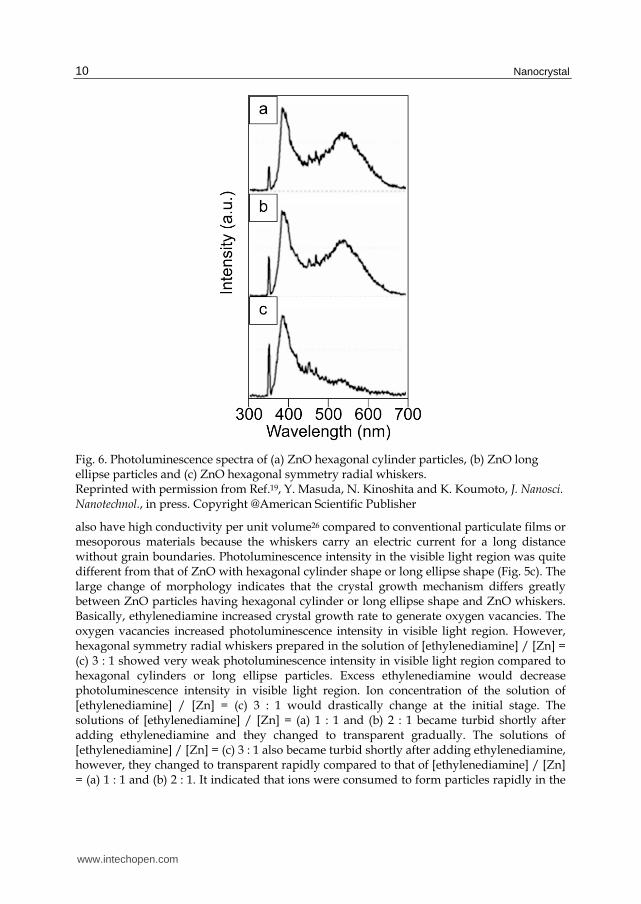
Fig. 4. SEM micrographs of (a) ZnO hexagonal cylinder particles, (b) ZnO long ellipse particles, (c1) ZnO hexagonal symmetry radial whiskers and (c2) magnified area of (c1). Reprinted with permission from Ref.19, Y. Masuda, N. Kinoshita and K. Koumoto, J. Nanosci. Nanotechnol., in press. Copyright @American Scientific Publisher
ZnO having hexagonal cylinder shape showed strong photoluminescence intensity in the UV region at about 370–400 nm and weak intensity in the visible light region at about 530–550 nm by 350 nm excitation light which appears in spectra (Fig. 6a). ZnO crystals were reported to show UV luminescence (around 390 nm) attributed to band-edge luminescence and visible-light luminescence caused from oxygen vacancy (450–600 nm)21,22. Oxygen vacancies would be generated in ZnO during crystallization to show visible-light luminescence. Concentration of ethylenediamine was increased twice to [ethylenediamine] / [Zn] = (b) 2 : 1. ZnO particles with long ellipse shape were deposited homogeneously from the solution (Fig. 4b). ZnO particles were about 100–200 nm in diameter and about 500 nm in length, and were similar to those of hexagonal cylinder shape. XRD showed the deposition to be well crystallized ZnO (Fig. 5b). Relative intensity of (10-10) diffraction is much stronger than that of (0002), indicating that mainly ZnO particles with long ellipse shape were laid on the silicon substrate. This was also observed in SEM micrographs (Fig. 4b). Deposition speed of ZnO with long ellipse shape was slightly faster than that of ZnO with hexagonal cylinder shape because of the high concentration of ethylenediamine. Ethylenediamine accelerates the crystallization of ZnO. In other words, supersaturation degree of the solution was increased by increasing the ethylenediamine concentration. As a result, ZnO grew slightly faster and formed not sharp hexagonal facets but rounded hexagonal cylinders, i.e., long ellipse shape. The photoluminescence spectrum of ZnO with long ellipse shape (Fig. 6b) was
www.intechopen.com

Morphology Control of Metal Oxide Nanocrystals
9
Fig. 5. XRD patterns of (a) ZnO hexagonal cylinder particles, (b) ZnO long ellipse particles, (c) ZnO hexagonal symmetry radial whiskers and ZnO (JCPDS No. 36-1451). Reprinted with permission from Ref.19, Y. Masuda, N. Kinoshita and K. Koumoto, J. Nanosci. Nanotechnol., in press. Copyright @American Scientific Publisher
similar to that of ZnO with hexagonal cylinder shape (Fig. 6a). The luminescence property was clearly shown to be stable and not influenced by the synthesis conditions in the range of [ethylenediamine] / [Zn] = 1 : 1 to 2 : 1. High repeatability and stability of the photoluminescence property without being affected by the deposition conditions are major advantages of this system for large-scale production. Further control the morphology was attempted by increasing the supersaturation degree. Ethylenediamine was added to the solution to be [ethylenediamine] / [Zn] = (c) 3 : 1 in the deposition process. ZnO whiskers were successfully grown and deposited from the solution. The morphology was drastically changed by the precise investigation and control of solution conditions. The whiskers were about 10–100 nm in diameter and about 1000–2000 nm in length (Fig. 4c1). A high aspect ratio was realized by high crystal growth rate of end faces to elongate the whiskers. Details of morphology were further evaluated. They were dispersed in water and dropped on a silicon substrate. Whiskers were connected to form hexagonal symmetry radial whiskers (Fig. 4c2). Six whiskers connected to form one particle. They had hexagonal symmetry. Tips of whiskers were finer than that at center of the particles. XRD showed the whiskers to be well crystallized ZnO (Fig. 5c). The relative intensity of (10-10) diffraction is much stronger than that of (0002), showing that mainly ZnO whiskers were laid on the substrate. This was also observed in SEM micrographs (Fig. 4c). Deposition of ZnO whiskers having high aspect ratio on the substrate would provide a ZnO network film having a high specific surface area. These whisker films can be applied to gas sensors23,24or solar cells25 which require high specific surface area. The whisker films
www.intechopen.com
Nanocrystal
10
Fig. 6. Photoluminescence spectra of (a) ZnO hexagonal cylinder particles, (b) ZnO long ellipse particles and (c) ZnO hexagonal symmetry radial whiskers. Reprinted with permission from Ref.19, Y. Masuda, N. Kinoshita and K. Koumoto, J. Nanosci. Nanotechnol., in press. Copyright @American Scientific Publisher
also have high conductivity per unit volume26 compared to conventional particulate films or mesoporous materials because the whiskers carry an electric current for a long distance without grain boundaries. Photoluminescence intensity in the visible light region was quite different from that of ZnO with hexagonal cylinder shape or long ellipse shape (Fig. 5c). The large change of morphology indicates that the crystal growth mechanism differs greatly between ZnO particles having hexagonal cylinder or long ellipse shape and ZnO whiskers. Basically, ethylenediamine increased crystal growth rate to generate oxygen vacancies. The oxygen vacancies increased photoluminescence intensity in visible light region. However, hexagonal symmetry radial whiskers prepared in the solution of [ethylenediamine] / [Zn] = (c) 3 : 1 showed very weak photoluminescence intensity in visible light region compared to hexagonal cylinders or long ellipse particles. Excess ethylenediamine would decrease photoluminescence intensity in visible light region. Ion concentration of the solution of [ethylenediamine] / [Zn] = (c) 3 : 1 would drastically change at the initial stage. The solutions of [ethylenediamine] / [Zn] = (a) 1 : 1 and (b) 2 : 1 became turbid shortly after adding ethylenediamine and they changed to transparent gradually. The solutions of [ethylenediamine] / [Zn] = (c) 3 : 1 also became turbid shortly after adding ethylenediamine, however, they changed to transparent rapidly compared to that of [ethylenediamine] / [Zn] = (a) 1 : 1 and (b) 2 : 1. It indicated that ions were consumed to form particles rapidly in the
www.intechopen.com
Morphology Control of Metal Oxide Nanocrystals
11
solution of [ethylenediamine] / [Zn] = (c) 3 : 1 and ion concentration would decrease drastically with color change. It can be assumed that high concentration of ethylenediamine increased crystal growth rate to form ZnO particles at the first stage. The particles generated in the first stage would not be whiskers but small ZnO particles. Ion concentration decreased rapidly to make solution transparent by formation of small particles because Zn ions were consumed in formation of the particles. ZnO whiskers would grow slowly on the small particles in dilute solutions at second stage. Consequently, hexagonal symmetry radial whiskers were formed in the solution of [ethylenediamine] / [Zn] = (c) 3 : 1. This phenomenon was consistent with reported ZnO whiskers which had high crystallinity, high photoluminescence intensity in UV region and low photoluminescence intensity in visible light region. Novel properties such as unique morphology, high specific surface area, high conductivity per unit volume, low photoluminescence intensity in visible light region and high photoluminescence intensity in UV region may pave the way to a new age of ZnO devices. Furthermore, they can be fabricated on low heat resistant materials such as polymers, paper or organic materials for flexible devices.
4. Morphology control of multi-needle ZnO particles and their particulate films
27
ZnO has attracted much attention as a next-generation gas sensor for CO28-30, NH331, NO232, H2S33, H229,34, ethanol34,35, SF634, C4H1034 or gasoline34 and dye-sensitized solar cells26,36-39. Sensitivity directly depends on the specific surface area of the sensing material. ZnO particles, particulate films or mesoporous material having high specific surface area were thus strongly required. ZnO has been crystallized to a hexagonal cylinder shape for gas sensors or solar cells in many studies26 by using the hexagonal crystal structure of ZnO at low supersaturation degree. However, strategic morphology design and precise morphology control for high specific surface area should be developed to improve the properties. ZnO particles should be controlled to have multi-needles or high surface asperity to increase the specific surface area by the crystallization at high supersaturation degree. Recently, morphology control20,40-42 and nano/micro manufacturing43-46 of oxide materials were proposed in solution systems. Solution systems have the advantage of adjustment of supersaturation degree and high uniformity in the system for particle morphology control. However, many factors affect the system compared to gas phase systems or solid state reactions. Solution chemistry for oxide materials is therefore being developed and many areas remain to be explored. Morphology control of ZnO particles to hexagonal cylinder shape, ellipse shape and multi-needle shape was recently developed20. Photoluminescence property was improved by changing the morphology and oxygen vacancy volume in this system. Morphology control of ZnO has also been proposed based on control of crystal growth47-50. W. Q. Peng et al. reported flower-like bunches synthesized on indium-doped tin oxide glass substrates through a chemical bath deposition process47. Y. R. Lin et al. fabricated nanowires on a ZnO-buffered silicon substrate by a hydrothermal method48. H. Zhang et al. prepared flowerlike, disklike, and dumbbell-like ZnO microcrystals by a capping-molecule-assisted hydrothermal process49. K. H. Liu et al. reported a hierarchical polygon prismatic Zn-ZnO core-shell structure grown on silicon by combining liquid-solution colloidals together with the vapor-gas growth process50. These studies showed high morphology controllability of
www.intechopen.com

Nanocrystal
12
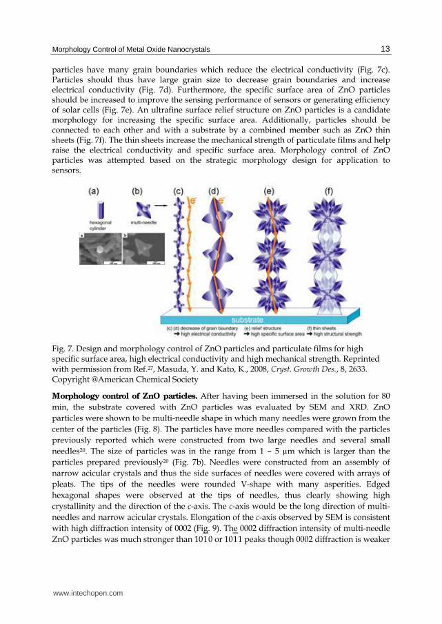
ZnO, however, morphology should be optimized to have high specific surface area to apply to solar cells or gas sensors. In this study, the morphology design of ZnO particles was proposed for solar cells or gas sensors in which high specific surface area, high electrical conductivity and high mechanical strength are required. Multi-needle ZnO particles having ultrafine surface relief structure, as well as particulate films constructed from multi-needle particles and thin sheets were fabricated27. Morphology control was realized based on a new idea inspired from the morphology change in our former study20. High supersaturation degree of the solution was used for fast crystal growth which induces the formation of multi-needle particles and low super saturation was used for the formation of ZnO thin sheets. Zinc nitrate hexahydrate (Zn(NO3)2 · 6H2O, > 99.0%, MW 297.49, Kanto Chemical Co., Inc.) and ethylenediamine (H2NCH2CH2NH2, > 99.0%, MW 60.10, Kanto Chemical Co., Inc.) were used as received. Glass (S-1225, Matsunami Glass Ind., Ltd.) was used as a substrate. Zinc nitrate hexahydrate (15 mM) was dissolved in distilled water at 60 °C and ethylenediamine (15 mM) was added to the solution to induce the formation of ZnO. Glass substrate was immersed in the middle of the solution at an angle and the solution was kept at 60 °C using a water bath for 80 min with no stirring. The solution became clouded shortly after the addition of ethylenediamine. Ethylenediamine plays an essential role in the formation of crystalline ZnO. ZnO was homogeneously nucleated and grown to form a large amount of particles to make the solution clouded. ZnO particles were gradually deposited and further grown on a substrate. Homogeneously nucleated particles precipitated gradually and the solution became light white after 80 min. The supersaturation degree of the solution was high at the initial stage of the reaction for the first 1 h and decreased as the color of the solution changed. ZnO particulate films constructed from ZnO particles and thin sheets were fabricated by immersion for 48 h. The glass substrate was immersed in the middle of the solution at an angle and the solution was kept at 60 °C using a water bath for 6 h with no stirring. The solution was then left to cool for 42 h in the bath. The solution became clouded shortly after the addition of ethylenediamine and clear after 6 h. The bottom of the solution was covered with white precipitate after 6 h. The supersaturation degree of the solution was high at the initial stage of the reaction for the first 1 h and then decreased as the color of the solution changed. Morphology of ZnO particles and particulate films was observed by a field emission scanning electron microscope (FE-SEM; JSM-6335FM, JEOL Ltd.) after heating at 150 °C for 30 min in vacuum for drying of carbon paste (Vacuum oven, VOS-201SD, EYELA, Tokyo Rikakikai. Co., Ltd.) and Pt coating for 3 nm (Quick cool coater, SC-701MCY, Sanyu Electronic Company). Crystal phases were evaluated by an X-ray diffractometer (XRD; RINT-2100V, Rigaku) with CuKα radiation (40 kV, 40 mA). Morphology design of ZnO particles and particulate films. The morphology of ZnO particles was designed to increase the specific surface area, electrical conductivity and mechanical strength of the base material of solar cells and sensors (Fig. 7). Typical ZnO particles grown at low supersaturation degree are shown in Fig. 7a20. The particles show edged hexagonal faces and elongate parallel to the c-axis. ZnO particles grow to have a hexagonal cylinder shape by slow crystal growth due to the hexagonal crystal structure of ZnO. The morphology of ZnO particles was controlled to have a multi-needle shape in an aqueous solution (Fig. 7b)20. Multi-needle particles have a high specific surface area compared to hexagonal cylinder particles, but particulate films constructed from small
www.intechopen.com
Morphology Control of Metal Oxide Nanocrystals
13
particles have many grain boundaries which reduce the electrical conductivity (Fig. 7c). Particles should thus have large grain size to decrease grain boundaries and increase electrical conductivity (Fig. 7d). Furthermore, the specific surface area of ZnO particles should be increased to improve the sensing performance of sensors or generating efficiency of solar cells (Fig. 7e). An ultrafine surface relief structure on ZnO particles is a candidate morphology for increasing the specific surface area. Additionally, particles should be connected to each other and with a substrate by a combined member such as ZnO thin sheets (Fig. 7f). The thin sheets increase the mechanical strength of particulate films and help raise the electrical conductivity and specific surface area. Morphology control of ZnO particles was attempted based on the strategic morphology design for application to sensors.
Fig. 7. Design and morphology control of ZnO particles and particulate films for high specific surface area, high electrical conductivity and high mechanical strength. Reprinted with permission from Ref.27, Masuda, Y. and Kato, K., 2008, Cryst. Growth Des., 8, 2633. Copyright @American Chemical Society
Morphology control of ZnO particles. After having been immersed in the solution for 80
min, the substrate covered with ZnO particles was evaluated by SEM and XRD. ZnO
particles were shown to be multi-needle shape in which many needles were grown from the
center of the particles (Fig. 8). The particles have more needles compared with the particles
previously reported which were constructed from two large needles and several small
needles20. The size of particles was in the range from 1 – 5 µm which is larger than the
particles prepared previously20 (Fig. 7b). Needles were constructed from an assembly of
narrow acicular crystals and thus the side surfaces of needles were covered with arrays of
pleats. The tips of the needles were rounded V-shape with many asperities. Edged
hexagonal shapes were observed at the tips of needles, thus clearly showing high
crystallinity and the direction of the c-axis. The c-axis would be the long direction of multi-
needles and narrow acicular crystals. Elongation of the c-axis observed by SEM is consistent
with high diffraction intensity of 0002 (Fig. 9). The 0002 diffraction intensity of multi-needle
ZnO particles was much stronger than 101_
0 or 101_
1 peaks though 0002 diffraction is weaker
www.intechopen.com

Nanocrystal
14
than 101_
0 or 101_
1 diffractions in randomly orientated ZnO particles (JCPDS No. 36-1451).
High diffraction intensity from (0002) planes which are perpendicular to the c-axis would be
caused from the crystalline ZnO particles which grew to elongate the c-axis. The particles
have more stacks of (0002) crystal planes compared to that of (101_
0) planes which are
parallel to the c-axis or (101_
1) planes and hence the intensity from (0002) planes was
stronger than that from (101_
0) or (101_
1) planes. ZnO grows to a hexagonal cylinder shape at low supersaturation degree because of its hexagonal crystal structure, however, ZnO grows to a multi-needle shape at high supersaturation degree which induces fast crystal growth. ZnO was thus grown to a multi-needle shape in our solution in spite of its hexagonal crystal structure. The growth of ZnO was halted by a rapid decrease of supersaturation degree and removal of particles from the solution to obtain ZnO multi-needle particles having an ultrafine surface relief structure. The morphology of the ZnO particles was controlled by the fast crystal growth due to high supersaturation degree and by the suppression of crystal growth due to the rapid decrease of supersaturation degree and removal of particles from the solution.
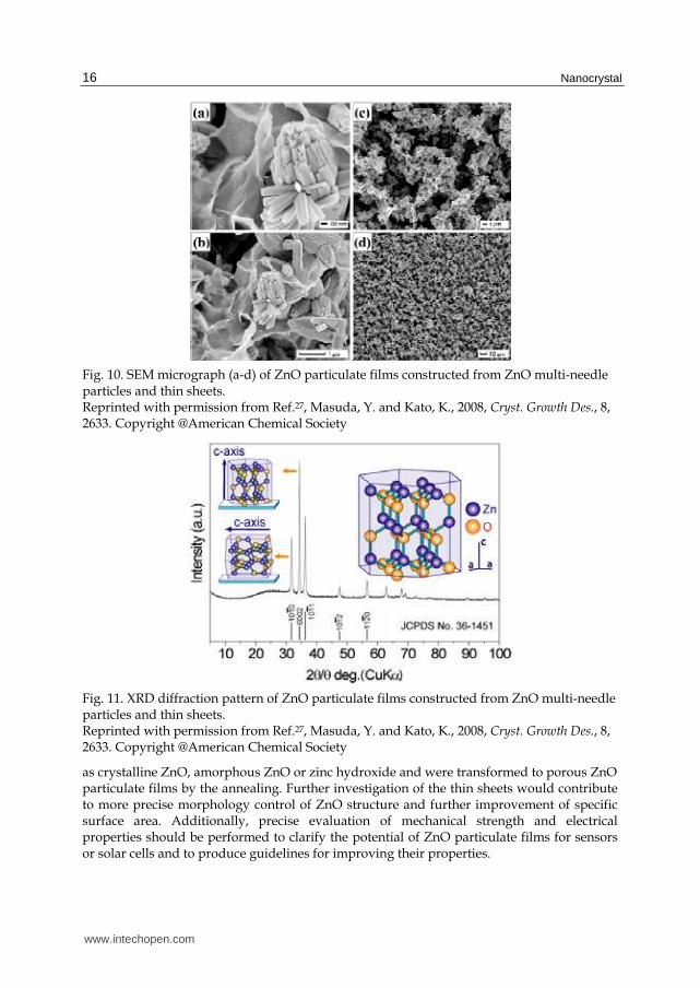
Fig. 8. SEM micrograph (a-d) of multi-needle ZnO particles having ultrafine surface relief structure. Reprinted with permission from Ref.27, Masuda, Y. and Kato, K., 2008, Cryst. Growth Des., 8, 2633. Copyright @American Chemical Society
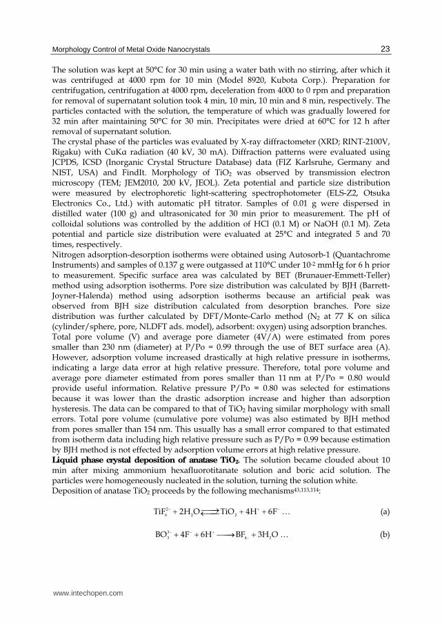
Morphology control of ZnO particulate films. ZnO particulate films showed a multi-needle shape and were connected to each other by thin sheets (Fig. 10a-c). The morphology of the particles was similar to that of the particles prepared by immersion for 80 min to have a high specific surface area. Thin sheets had a thickness of 10 – 50 nm and width of 1 – 10 µm and were connected to particles closely with no clearance. The particulate films had continuous open pores ranging from several nm to 10 µm in diameter. The particulate films showed x-ray diffraction patterns of ZnO crystal with no additional phase (Fig. 11). Diffraction peaks were very sharp, showing high crystallinity of the particulate films. The high intensity of 0002 would be caused by elongation of multi-needle particles in the c-axis direction which increases the stacks of (0002) crystal planes.
www.intechopen.com

Morphology Control of Metal Oxide Nanocrystals
15
Fig. 9. XRD diffraction pattern of multi-needle ZnO particles having ultrafine surface relief structure. Reprinted with permission from Ref.27, Masuda, Y. and Kato, K., 2008, Cryst. Growth Des., 8, 2633. Copyright @American Chemical Society
ZnO multi-needle particles having an ultrafine surface relief structure were prepared at 60 °C in the white solution during the initial 80 min (Fig. 7e). The supersaturation degree was high at the initial stage of the reaction due to the high concentration of ions. ZnO particles were then precipitated, making the bottom of the solution white and the solution itself clear. Ions were consumed to form ZnO particles and thus the ion concentration of the solution decreased rapidly. Thin sheets were formed at 25 °C in the clear solution after the formation of multi-needle particles (Fig. 7f). Solution temperature and supersaturation degree would influence on precipitates. Consequently, the particulate films constructed from multi-needle particles and thin sheets were successfully fabricated by the two-step growth (Fig. 7f). For comparison, assemblies of thin sheets were prepared at air-liquid interfaces of the same solution we used in this study51. XRD patterns of the sheets were assigned to ZnO. The sheets had c-axis orientation parallel to the sheets, i.e., in-plane c-axis orientation. TEM observations showed the sheets were dense polycrystals consisted of nano-sized ZnO crystals. Electron diffraction pattern showed strong isotropic diffraction ring from (0002) planes. It suggested in-plane c-axis orientation of ZnO crystals which was consistent with XRD evaluations. Mechanical strength and electrical property would be affected by crystal orientation and microstructures. The sheets would have stronger mechanical strength compared to porous sheets because of their dense structure. They would have different electrical properties from randomly oriented sheets due to in-plane c-axis orientation, because ZnO has anisotropic electrical properties caused from anisotropic hexagonal crystal structure. The sheets prepared at air-liquid interfaces51 would be similar to that prepared in the solutions (Fig. 10) because both of them were prepared from the same solution and showed XRD patterns assigned to ZnO51 (Fig. 11). The sheets prepared in this study (Fig. 4, 5) would have similar mechanical and electrical properties to the sheets prepared at air-liquid interfaces51. Thin sheets were transformed to particles and porous particulate films by annealing at 500 °C for 1 h in air. The sheets did not maintain their thin sheet shape due to high slimness and/or phase transformation. Thin sheets would be inorganic films containing Zn ions such
www.intechopen.com
Nanocrystal
16
Fig. 10. SEM micrograph (a-d) of ZnO particulate films constructed from ZnO multi-needle particles and thin sheets. Reprinted with permission from Ref.27, Masuda, Y. and Kato, K., 2008, Cryst. Growth Des., 8, 2633. Copyright @American Chemical Society
Fig. 11. XRD diffraction pattern of ZnO particulate films constructed from ZnO multi-needle particles and thin sheets. Reprinted with permission from Ref.27, Masuda, Y. and Kato, K., 2008, Cryst. Growth Des., 8, 2633. Copyright @American Chemical Society
as crystalline ZnO, amorphous ZnO or zinc hydroxide and were transformed to porous ZnO
particulate films by the annealing. Further investigation of the thin sheets would contribute to more precise morphology control of ZnO structure and further improvement of specific surface area. Additionally, precise evaluation of mechanical strength and electrical properties should be performed to clarify the potential of ZnO particulate films for sensors or solar cells and to produce guidelines for improving their properties.
www.intechopen.com

Morphology Control of Metal Oxide Nanocrystals
17
Multi-needle ZnO particles having an ultrafine surface relief structure were successfully fabricated by the precise control of crystal growth in an aqueous solution. The morphology of ZnO was further controlled for ZnO particulate films constructed from ZnO multi-needle particles and thin sheets. The thin sheets connected particles to each other and with a substrate. The morphology design and morphology control described here will facilitate the progress of crystal science for developing future advanced materials and devices.
5. Morphology control of high c-axis oriented stand-alone ZnO self-assembled film
51
Recently, crystalline ZnO20,26,47-50,52-59 have been synthesized to utilize the high potential of the solution process for future devices and to realize green chemistry for a sustainable society. For instance, ZnO nanowire arrays have been synthesized using seed layers in aqueous solutions for dye-sensitized solar cell26,52. Full sun efficiency of 1.5% is demonstrated in this study. O’Brien et al. prepared specular ZnO films consisting of clumps of elongated triangular crystals53, small ZnO spherical clumps consisting of particles of ca. 100 nm53, ZnO films consisting of randomly rod-shaped particles of up to 1000 nm in length53, ZnO films consisting of very thin random rod-shaped particles of ca. 1000 nm53 and specular films consisting of flowers with well-formed triangle features59 in aqueous solutions. However, ZnO films have usually been prepared on substrates54,57,60-76, and in particular crystalline ZnO films having high c-axis orientation require expensive substrates such as single crystals or highly-functional substrates. A simple and low-cost process for self-supporting crystalline ZnO films is expected to be used for a wide range of applications such as windows of optical devices or low-value-added products. Self-supporting crystalline ZnO films can also be applied by being pasting on a desired substrate such as low heat-resistant polymer films, glasses, metals or papers. In this section, high c-axis oriented stand-alone ZnO self-assembled films was fabricated using an air-liquid interface51. ZnO was crystallized from an aqueous solution without heat treatment or catalyst. The ZnO film was fabricated at the air-liquid interface without using ammonia vapor. Zinc nitrate hexahydrate (Zn(NO3)2 · 6H2O, > 99.0%, MW 297.49, Kanto Chemical Co., Inc.) and ethylenediamine (H2NCH2CH2NH2, > 99.0%, MW 60.10, Kanto Chemical Co., Inc.) were used as received. Zinc nitrate hexahydrate (15 mM) was dissolved in distilled water at 60°C and ethylenediamine (15 mM) was added to the solution to induce the formation of ZnO. The solution was kept at 60°C using a water bath for 6 h with no stirring. The solution was then left to cool for 42 h in the bath. Polyethylene terephthalate (PET) film, glass (S-1225, Matsunami Glass Ind., Ltd.) and an Si wafer (p-type Si [100], NK Platz Co., Ltd.) were used as substrates. Morphology of ZnO film was observed by a field emission scanning electron microscope (FE-SEM; JSM-6335FM, JEOL Ltd.) and a transmission electron microscope (TEM; H-9000UHR, 300 kV, Hitachi). Crystal phase was evaluated by an X-ray diffractometer (XRD; RINT-2100V, Rigaku) with CuKα radiation (40 kV, 40 mA). Si wafer was used as a substrate for XRD evaluation. The crystal structure model and diffraction pattern of ZnO were calculated from ICSD (Inorganic Crystal Structure Database) data No. 26170 (FIZ Karlsruhe, Germany and NIST, USA) using FindIt and ATOMS (Hulinks Inc.). The solution became clouded shortly after the addition of ethylenediamine by the homogeneous nucleation and growth of ZnO particles. ZnO particles were gradually
www.intechopen.com

Nanocrystal
18
deposited to cover the bottom of the vessel, and the solution became light white after 1 h and clear after 6 h. The supersaturation degree of the solution was high at the initial stage of the reaction for the first 1 h and decreased as the color of the solution changed. White films were formed at the air-liquid interface and they grew to large films. The films had sufficiently high strength to be obtained as stand-alone films. Additionally, a film was scooped to past onto a desired substrate such PET film, Si wafer, glass plate or paper, and the pasted ZnO film was then dried to bond it to the substrate. Both sides of the film can be pasted on substrate. The film physically adhered to the substrate. The film maintained its adhesion during immersion in lightly ultrasonicated water, however, it can be easily peeled off again by strong ultrasonication. The film can be handled easily from substrate to other substrate. It also can be attached strongly to substrate by annealing or addition of chemical regents such as silane coupling agent to form chemical bonds between the film and the substrate The film grew to a thickness of about 5 µm after 48 h, i.e., 60°C for 6 h, and was left to cool for 42 h. The air side of the stand-alone film had a smooth surface over a wide area due to the flat air-liquid interface (Fig. 12-a1), whereas the liquid side of the film had a rough surface (Fig. 12-b1). The films consisted of ZnO nano-sheets were clearly observed from the liquid side (Fig. 12-b2) and the fracture edge-on profile of the film (Fig. 12-c1, 12-c2). The nano-sheets had a thickness of 5-10 nm and were 1-5 µm in size. They mainly grew forward to the bottom of the solution, i.e., perpendicular to the air-liquid interface, such that the sheets stood perpendicular to the air-liquid interface. Thus, the liquid side of the film had many ultra-fine spaces surrounded by nano-sheet and had a high specific surface area. The air side of the film, on the other hand, had a flat surface that followed the flat shape of the air-liquid interface. The air-liquid interface was thus effectively utilized to form the flat surface of the film. This flatness would contribute to the strong adhesion strength to substrates for pasting of the film. The air-side surface prepared for 48 h had holes of 100-500 nm in diameter (Fig. 12-a2), and were hexagonal, rounded hexagonal or round in shape. The air-side surface prepared for 6 h, in contrast, had no holes on the surface. The air-side surface was well crystallized to form a dense surface and ZnO crystals would partially grow to a hexagonal shape because of the hexagonal crystal structure. Well-crystallized ZnO hexagons were then etched to form holes on the surface by decrease in pH. The growth face of the film would be liquid side. ZnO nano-sheets would grow to form a large ZnO film by Zn ion supply from the aqueous solution. Further investigation of the formation mechanism would contribute to the development of crystallography in the solution system and the creation of novel ZnO fine structures. The film showed a very strong 0002 x-ray diffraction peak of hexagonal ZnO at 2θ = 34.04° and weak 0004 diffraction peak at 2θ = 72.16° with no other diffractions of ZnO (Fig. 13). (0002) planes and (0004) planes were perpendicular to the c-axis, and the diffraction peak only from (0002) and (0004) planes indicates high c-axis orientation of ZnO film. The inset figure shows that the crystal structure of hexagonal ZnO stands on a substrate to make the c-axis perpendicular to the substrate. Crystallite size parallel to (0002) planes was estimated from the half-maximum full-width of the 0002 peak to 43 nm. This is similar to the threshold limit value of our XRD equipment and thus the crystallite size parallel to (0002) planes is estimated to be greater than or equal to 43 nm. Diffraction peaks from a silicon substrate were observed at 2θ = 68.9° and 2θ = 32.43°. Weak diffractions at 2θ = 12.5°, 24.0°, 27.6°, 30.5°, 32.4° and 57.6° were assigned to co-precipitated zinc carbonate hydroxide (Zn5(CO3)2(OH)6, JCPDS No. 19-1458).
www.intechopen.com

Morphology Control of Metal Oxide Nanocrystals
19
Fig. 12. SEM micrographs of high c-axis oriented stand-alone ZnO self-assembled film. (a1) Air-side surface of ZnO film. (a2) Magnified area of (a1). (b1) Liquid-side surface of ZnO film. (b2) Magnified area of (b2). (c1) Fracture cross section of ZnO film from air side. (c2) Magnified area of (c1). Reprinted with permission from Ref.51, Masuda, Y. and Kato, K., 2008, Cryst. Growth Des., 8, 275. Copyright @American Chemical Society
Stand-alone ZnO film was further evaluated by TEM and electron diffraction. The film was crushed to sheets and dispersed in an acetone. The sheets at the air-liquid interface were skimmed by a cupper grid with a carbon supporting film. The sheets were shown to have uniform thickness (Fig. 14a). They were dense polycrystalline films constructed of ZnO nanoparticles (Fig. 14b). Lattice image was clearly observed to show high crystallinity of the particles. The film was shown to be single phase of ZnO by electron diffraction pattern. These observations were consistent with XRD and SEM evaluations. The film pasted on a silicon wafer was annealed at 500°C for 1 h in air to evaluate the details of the films. ZnO film maintained its structure during the annealing (Fig. 15). The air side of the film showed a smooth surface (Fig. 15-a1) and the liquid side showed a relief structure having a high specific surface area (Fig. 15-b1, 15-b2). The air side showed the film consisted of dense packing of small ZnO nanosheets and the size of sheets increased toward the liquid-side surface (Fig. 15-a2). ZnO sheets would grow from the air side to the liquid side, i.e., the sheets would nucleate at the liquid-air interface and grow down toward the bottom of the solution by the supply of Zn ions from the solution. Annealed film showed X-ray diffractions of ZnO and Si substrate with no additional phases. As-deposited ZnO nano-sheets were shown to be crystalline ZnO because the sheets maintained their fine structure during the annealing without any phase transition. High c-axis orientation was also maintained during the annealing, showing a very strong 0002 diffraction peak.
www.intechopen.com

Nanocrystal
20
Fig. 13. XRD diffraction pattern of high c-axis oriented stand-alone ZnO self-assembled film. Reprinted with permission from Ref.51, Masuda, Y. and Kato, K., 2008, Cryst. Growth Des., 8, 275. Copyright @American Chemical Society
Fig. 14. (a) TEM micrograph of ZnO nano-sheets. (b) Magnified area of (a). (Insertion) Electron diffraction pattern of ZnO. Reprinted with permission from Ref.51, Masuda, Y. and Kato, K., 2008, Cryst. Growth Des., 8, 275. Copyright @American Chemical Society
www.intechopen.com

Morphology Control of Metal Oxide Nanocrystals
21
Fig. 15. SEM micrographs of high c-axis oriented stand-alone ZnO self-assembled film annealed at 500°C for 1 h in air. (a1) Fracture edge-on profile of ZnO film from air side. (a2) Cross-section profile of ZnO film from air side. (b1) Fracture edge-on profile of ZnO film from liquid side. (b2) Cross-section profile of ZnO film from liquid side. Reprinted with permission from Ref.51, Masuda, Y. and Kato, K., 2008, Cryst. Growth Des., 8, 275. Copyright @American Chemical Society
The solution was further kept at 25°C for 1 month to evaluate the details of the deposition mechanism. The film prepared at the air-liquid interface for 1 month was not hexagonal
ZnO. The film showed strong X-ray diffractions of zinc carbonate hydroxide single phase. ZnO would be dissolved by decrease in pH. ZnO would be crystallized at the initial reaction stage for the first 48 h. ZnO was then gradually etched and dissolved by nitric acid and zinc carbonate hydroxide was crystallized using Zn ions which were supplied by the dissolution
of crystalline ZnO. High c-axis oriented stand-alone ZnO self-assembled film was fabricated using a simple solution process. The film consisted of ZnO nanosheets was crystallized at air-liquid
interface. The nanosheets grew perpendicular to the film. The film had high c-axis orientation and showed a strong 0002 diffraction peak and weak 0004 peak. The air side of the film had a flat surface, whereas the liquid side had a rough surface having many ultra-fine spaces surrounded by ZnO nano-sheets. The rough surface of the liquid side can be
utilized for sensors or dye-sensitized solar cells. The ZnO film was also pasted on a desired substrate such as PET films, Si substrate or glass plates. The surface of low heat-resistant flexible polymer film was modified with high c-axis oriented crystalline ZnO film without heat treatment. This low-cost, low-temperature technique can be used for a wide range of
applications including sensors, solar cells, electrical devices and optical devices using the various properties of high c-axis oriented crystalline ZnO.
www.intechopen.com

Nanocrystal
22
6. Morphology control of nanocrystal assembled TiO2 particles77
Anatase TiO2 particles, 100–200 nm in diameter, were developed in aqueous solution at 50°C. The particles were assemblies of nano TiO2 crystals covered with nanorelief surface structures. The crystals grew anisotropically along the c-axis to form acicular crystals. The particles showed c-axis orientation due to high-intensity X-ray diffraction from the (004) planes. The particles had a BET specific surface area of 270 m2/g. BJH and DFT/Monte-Carlo analysis of adsorption isotherm indicated the existence of pores ~3 nm and ~1 nm in diameter. Crystallization and self-assembly of nano TiO2 were effectively utilized to fabricate nanocrystal assembled TiO2 particles having high surface area and nanorelief surface structure. Nanoporous TiO2 architecture with micropores (<2 nm), mesopores (2–50 nm) and/or macropores (>50 nm) is of considerable interest for both scientific and technical applications. The latter include cosmetics, catalysts78, photocatalysts79-82, gas sensors83,84, lithium batteries85-87, biomolecular sensors88 and dye-sensitized solar cells89,90. Crystalline anatase generally exhibits higher properties than rutile in photocatalysts, biomolecular sensors and dye-sensitized solar cells. Electrons are obtained from dyes adsorbed on TiO2 electrodes in sensors and solar cells. Photoelectric conversion efficiency strongly depends on dye adsorption volume and surface area of TiO2. High surface area is required to achieve high efficiency and sensitivity of the devices. Additionally, the surface of TiO2 should be covered with nano/microrelief structures to adsorb large amounts of dye, molecules and DNA for biomolecular sensors and dye-sensitized solar cells. TiO2 nanoparticles have been prepared by flame synthesis91,92, ultrasonic irradiation93,94, chemical vapor synthesis95, sol-gel methods79,96-100, sonochemical method101 and liquid phase deposition of amorphous TiO2102-105. High temperature in the treatment processes, however, causes aggregation of nanoparticles and decreased surface area. Formation of nanorelief structures on the surface of the particles is difficult to achieve in these processes. Highly porous materials have been prepared via template-based methods, including soft templates (surfactants, chelating agents, block polymers, etc.)106-109 and hard templates (porous anionic alumina, porous silica, polystyrene spheres, carbon nanotubes, etc.)110,111. However, the nanostructures of these materials usually change due to amorphous-phase crystallization to anatase TiO2 during annealing. This decreases the surface area and damages the surface nanostructures. In this section, porous anatase TiO2 particles were developed in aqueous solution. Nano TiO2 was crystallized in the solution to assemble into particles 100–200 nm in diameter. The surface of the particles was covered with nanorelief structures. The particles showed c-axis orientation due to anisotropic crystal growth of TiO2 along the c-axis. BET surface area of the particles was estimated to be 270 m2/g112. BJH and DFT/Monte-Carlo analysis of adsorption isotherm indicated the existence of pores ~2.8 nm and ~3.6 nm in diameter, respectively. The existence of micropores ~1 nm was also indicated. Crystallization and self-assembly of acicular TiO2 were effectively utilized to fabricate nanocrystal assembled TiO2 particles having high surface area and nanorelief surface structure. Ammonium hexafluorotitanate ([NH4]2TiF6) (Morita Chemical Industries Co., Ltd., FW: 197.95, purity 96.0%) and boric acid (H3BO3) (Kishida Chemical Co., Ltd., FW: 61.83, purity 99.5%) were used as received. Ammonium hexafluorotitanate (12.372 g) and boric acid (11.1852 g) were separately dissolved in deionized water (600 mL) at 50°C. Boric acid solution was added to ammonium hexafluorotitanate solution at a concentration of 0.15 and 0.05 M, respectively.
www.intechopen.com
Morphology Control of Metal Oxide Nanocrystals
23
The solution was kept at 50°C for 30 min using a water bath with no stirring, after which it was centrifuged at 4000 rpm for 10 min (Model 8920, Kubota Corp.). Preparation for centrifugation, centrifugation at 4000 rpm, deceleration from 4000 to 0 rpm and preparation for removal of supernatant solution took 4 min, 10 min, 10 min and 8 min, respectively. The particles contacted with the solution, the temperature of which was gradually lowered for 32 min after maintaining 50°C for 30 min. Precipitates were dried at 60°C for 12 h after removal of supernatant solution. The crystal phase of the particles was evaluated by X-ray diffractometer (XRD; RINT-2100V, Rigaku) with CuKα radiation (40 kV, 30 mA). Diffraction patterns were evaluated using JCPDS, ICSD (Inorganic Crystal Structure Database) data (FIZ Karlsruhe, Germany and NIST, USA) and FindIt. Morphology of TiO2 was observed by transmission electron microscopy (TEM; JEM2010, 200 kV, JEOL). Zeta potential and particle size distribution were measured by electrophoretic light-scattering spectrophotometer (ELS-Z2, Otsuka Electronics Co., Ltd.) with automatic pH titrator. Samples of 0.01 g were dispersed in distilled water (100 g) and ultrasonicated for 30 min prior to measurement. The pH of colloidal solutions was controlled by the addition of HCl (0.1 M) or NaOH (0.1 M). Zeta potential and particle size distribution were evaluated at 25°C and integrated 5 and 70 times, respectively. Nitrogen adsorption-desorption isotherms were obtained using Autosorb-1 (Quantachrome Instruments) and samples of 0.137 g were outgassed at 110°C under 10-2 mmHg for 6 h prior to measurement. Specific surface area was calculated by BET (Brunauer-Emmett-Teller) method using adsorption isotherms. Pore size distribution was calculated by BJH (Barrett-Joyner-Halenda) method using adsorption isotherms because an artificial peak was observed from BJH size distribution calculated from desorption branches. Pore size distribution was further calculated by DFT/Monte-Carlo method (N2 at 77 K on silica (cylinder/sphere, pore, NLDFT ads. model), adsorbent: oxygen) using adsorption branches. Total pore volume (V) and average pore diameter (4V/A) were estimated from pores smaller than 230 nm (diameter) at P/Po = 0.99 through the use of BET surface area (A). However, adsorption volume increased drastically at high relative pressure in isotherms, indicating a large data error at high relative pressure. Therefore, total pore volume and average pore diameter estimated from pores smaller than 11 nm at P/Po = 0.80 would provide useful information. Relative pressure P/Po = 0.80 was selected for estimations because it was lower than the drastic adsorption increase and higher than adsorption hysteresis. The data can be compared to that of TiO2 having similar morphology with small errors. Total pore volume (cumulative pore volume) was also estimated by BJH method from pores smaller than 154 nm. This usually has a small error compared to that estimated from isotherm data including high relative pressure such as P/Po = 0.99 because estimation by BJH method is not effected by adsorption volume errors at high relative pressure. Liquid phase crystal deposition of anatase TiO2. The solution became clouded about 10 min after mixing ammonium hexafluorotitanate solution and boric acid solution. The particles were homogeneously nucleated in the solution, turning the solution white. Deposition of anatase TiO2 proceeds by the following mechanisms43,113,114:
2
6 2 2TiF 2H O TiO 4H 6F … (a)
3
3 4 2BO 4F 6H BF 3H O
… (b)
www.intechopen.com

Nanocrystal
24
Equation (a) is described in detail by the following two equations:
2 2 2nOH (6 n )OH
6 6 n n 6TiF TiF (OH) nF Ti(OH) 6F
… (c)
2
6 2 2Ti(OH) TiO 2H O 2OH … (d)
Fluorinated titanium complex ions gradually change into titanium hydroxide complex ions in an aqueous solution, as shown in Eq. (c). The increase of F- concentration displaces Eqs. (a) and (c) to the left; however, the produced F- can be scavenged by H3BO3 (BO33-) as shown in Eq. (b) to displace Eqs. (a) and (c) to the right. Anatase TiO2 is formed from titanium hydroxide complex ions (Ti(OH)62-) in Eq. (d). Crystal phase of TiO2 particles. X-ray diffraction peaks for the particles were observed at 2θ = 25.1, 37.9, 47.6, 54.2, 62.4, 69.3, 75.1, 82.5 and 94.0° after evaluation of N2 adsorption. They were assigned to the 101, 004, 200, 105 + 211, 204, 116 + 220, 215, 303 + 224 + 312 and 305 + 321 diffraction peaks of anatase TiO2 (JCPSD No. 21-1272, ICSD No. 9852) (Fig. 16). The 004 diffraction intensity of randomly oriented particles is usually 0.2 times the 101 diffraction intensity as shown in JCPDS data (No. 21-1272). However, the 004 diffraction intensity of the particles deposited in our process was 0.36 times the 101 diffraction intensity. Additionally, the integral intensity of the 004 diffraction was 0.18 times the 101 diffraction intensity, indicating the c-axis orientation of the particles. Particles were not oriented on the glass holder for XRD measurement. Therefore, TiO2 crystals would be an anisotropic shape in which the crystals were elongated along the c-axis. The crystals would have a large number of stacks of c planes such as (001) planes compared to stacks of (101) planes. The diffraction intensity from the (004) planes would be enhanced compared to that from the (101) planes. Crystallite size perpendicular to the (101) or (004) planes was estimated from the full-width half-maximum of the 101 or 004 peak to be 3.9 nm or 6.3 nm, respectively. Elongation of crystals in the c-axis direction was also suggested by the difference in crystallite size. TEM observation of TiO2 particles. The particles were shown to be assemblies of nano TiO2 crystals (Fig. 17a). Particle diameter was estimated to be 100–200 nm. Relief structures had formed on the surfaces and open pores had formed inside because the particles were porous assemblies of nanocrystals. Nanocrystals were shown to have acicular shapes (Fig. 17b). They were about 5–10 nm in length. The longer direction of acicular TiO2 is indicated by the black arrow. The inserted FFT image shows the 101 and 004 diffractions of anatase TiO2. Nanocrystals are assigned to the single phase of anatase TiO2. It is notable that the diffraction from the (101) planes has a ring shape due to random orientation but that from the (004) planes was observed only in the upper right region and lower left region in the FFT image. Anisotropic 004 diffractions indicated the direction of the c-axis, which was perpendicular to the (004) planes, as shown by the white arrow. It was roughly parallel to the longer direction of acicular TiO2. These results suggest that acicular TiO2 grew along the c-axis to enhance the diffraction intensity from the (004) planes. Crystal growth of anatase TiO2 along the c-axis was previously observed in TiO2 films113. Anisotropic crystal growth is one of the features of liquid phase crystal deposition. Acicular nanocrystals showed lattice images of anatase TiO2 (Fig. 17c). They were constructed of anatase TiO2 crystals without amorphous or additional phases. Anatase crystals were not covered with amorphous or additional phases even at the tips. Bare
www.intechopen.com

Morphology Control of Metal Oxide Nanocrystals
25
anatase crystal with nanosized structure is important to achieve high performance for catalysts and devices.
Fig. 16. XRD diffraction pattern of anatase TiO2 particles. Reprinted with permission from Ref.77, Masuda, Y. and Kato, K., 2008, Cryst. Growth Des., 8, 3213. Copyright @American Chemical Society
Crystallization of TiO2 was effectively utilized to form assemblies of acicular nanocrystals in the process. Open pores and surface relief structures were successfully formed on the particles.
Fig. 17. (a): TEM micrograph of anatase TiO2 particles. (b): Magnified area of (a) showing morphology of acicular crystals. Insertion in (b): FFT image of (b) anatase TiO2. (c): Magnified area of (a) showing lattice images of anatase TiO2. Reprinted with permission from Ref.77, Masuda, Y. and Kato, K., 2008, Cryst. Growth Des., 8, 3213. Copyright @American Chemical Society
Zeta potential and particle size distribution. The dried particles were dispersed in water to evaluate zeta potential and particle size distribution after evaluation of N2 adsorption. The particles had positive zeta potential of 30.2 mV at pH 3.1, which decreased to 5.0, −0.6, −11.3 and −36.3 mV at pH 5.0, 7.0, 9.0 and 11.1, respectively (Fig. 18). The isoelectric point was estimated to be pH 6.7, slightly higher than that of anatase TiO2 (pH 2.7–6.0)115. Zeta
www.intechopen.com

Nanocrystal
26
potential is very sensitive to the particle surface conditions, ions adsorbed on the particle surfaces, and the kind and concentration of ions in the solution. The variations in zeta potential were likely caused by the difference in the surface conditions of TiO2 particles, affected by the interaction between particles and ions in the solution.
Fig. 18. Zeta potential of anatase TiO2 particles as a function of pH. Reprinted with permission from Ref.77, Masuda, Y. and Kato, K., 2008, Cryst. Growth Des., 8, 3213. Copyright @American Chemical Society
Mean particle size was estimated to be ~550 nm in diameter with a standard deviation (STD) of 220 nm at pH 3.1 (Fig. 19a). This was larger than that observed by TEM. Slight aggregation occurred at pH 3 because the particles were dried completely prior to measurement. Particle size increased with pH and showed a maximum of near the isoelectric point (550 nm at pH 3.1, 3150 nm at pH 5, 4300 nm at pH 7, 5500 nm at pH 9 or 2400 nm at pH 11.1) (Fig. 19b). Strong aggregation resulted from the lack of repulsion force between particles near the isoelectric point. The particles were generated in the solution at pH 3.8 in this study. It would be suitable to obtain repulsion force between particles for crystallization without strong aggregation. N2 adsorption characteristics of TiO2 particles. TiO2 particles exhibited N2 adsorption-desorption isotherms of Type IV (Fig. 20a). The desorption isotherm differed from adsorption isotherm in the relative pressure (P/P0) range from 0.4 to 0.7, showing mesopores in the particles. BET surface area of the particles was estimated to be 270 m2/g (Fig. 20b). This is higher than that of TiO2 nanoparticles such as Aeroxide P25 (BET 50 m2/g, 21 nm in diameter, anatase 80% + rutile 20%, Degussa), Aeroxide P90 (BET 90–100 m2/g, 14 nm in diameter, anatase 90% + rutile 10%, Degussa), MT-01 (BET 60 m2/g, 10 nm in diameter, rutile, Tayca Corp.) and Altair TiNano (BET 50 m2/g, 30–50 nm in diameter, Altair Nanotechnologies Inc.)116. A high BET surface area cannot be obtained from particles having a smooth surface even if the particle size is less than 100 nm. A high BET surface area would be realized by the unique morphology of TiO2 particles constructed of nanocrystal assemblies. Total pore volume and average pore diameter were estimated from pores smaller than 230 nm at P/Po = 0.99–0.431 cc/g and 6.4 nm, respectively. They were estimated to be 0.212 cc/g and 3.1 nm, respectively, from pores smaller than 11 nm at P/Po = 0.80. Total pore volume was also estimated by the BJH method from pores smaller than 154 nm to be 0.428 cc/g. Average pore diameter was estimated to be 6.3 nm using BET surface area.
www.intechopen.com

Morphology Control of Metal Oxide Nanocrystals
27
Fig. 19. (a): Particle size distribution of anatase TiO2 particles at pH 3.1. (b): Particle size of anatase TiO2 particles as a function of pH. Reprinted with permission from Ref.77, Masuda, Y. and Kato, K., 2008, Cryst. Growth Des., 8, 3213. Copyright @American Chemical Society
Pore size distribution was calculated by the BJH method using adsorption isotherms (Fig. 20c). It showed a pore size distribution curve having a peak at ~2.8 nm and pores larger than 10 nm. TiO2 particles would have mesopores of ~2.8 nm surrounded by nanocrystals. Pores larger than 10 nm are considered to be interparticle spaces. The pore size distribution also suggested the existence of micropores smaller than 1 nm. Pore size distribution was further calculated by the DFT/Monte-Carlo method. The model was in fair agreement with adsorption isotherms (Fig. 20d). Pore size distribution showed a peak at ~3.6 nm that indicated the existence of mesopores of ~3.6 nm (Fig. 20e). The pore size calculated by the DFT/Monte-Carlo method was slightly larger than that calculated from the BJH method because the latter method is considered to have produced an underestimation117-119. The pore size distribution also suggested the existence of micropores of ~1 nm, probably resulting from microspaces surrounded by nanocrystals and the uneven surface structure of nanocrystals. The particles were shown to have a large surface area as well as micropores of ~1 nm, mesopores of ~2.8–3.6 nm and pores larger than 10 nm, by N2 adsorption characteristics. Assembly of acicular nanocrystals resulted in unique features and high surface area. TiO2 particles were generated in the solutions at 90°C for 1h using an oil bath with no stirring for comparison. The solutions became clouded after the addition of boric acid solutions into ammonium hexafluorotitanate solutions. High temperature accelerated
www.intechopen.com

Nanocrystal
28
Fig 20. (a): N2 adsorption-desorption isotherm of anatase TiO2 particles. (b): BET surface area of anatase TiO2 particles. (c): Pore size distribution calculated from N2 adsorption data of anatase TiO2 particles using BJH equation. (d): N2 adsorption-desorption isotherm and DFT/Monte-Carlo fitting curve of anatase TiO2 particles. (e): Pore size distribution calculated from N2 adsorption data of anatase TiO2 particles using DFT/Monte-Carlo equation. Reprinted with permission from Ref.77, Masuda, Y. and Kato, K., 2008, Cryst. Growth Des., 8, 3213. Copyright @American Chemical Society
crystal growth of TiO2. Hydrogen chloride of 0.6 ml was added into the solutions of 200ml to decrease crystallization speed of TiO2. The pH of the solutions was 2.4 one hour after mixing the solutions. BET surface area of the particles was estimated to 18 m2/g. This is much lower than that of the particles prepared at 50°C and slightly lower than that prepared at 90°C for 8 min in our previous work (44 m2/g)120. Formation of TiO2 was accelerated at high temperature and it decreased surface area. The particles grew in the solutions to
www.intechopen.com
Morphology Control of Metal Oxide Nanocrystals
29
decrease surface area as function of time. Crystallization of TiO2 was shown to be strongly affected by growth conditions such as solution temperature and growth time. Anatase TiO2 particles, 100–200 nm in diameter, were successfully fabricated in aqueous solution. They were assemblies of nanocrystals 5–10 nm that grew anisotropically along the c-axis to form acicular shapes. The particles thus had nanorelief surface structures constructed of acicular crystals. They showed c-axis orientation due to high-intensity X-ray diffraction from the (004) crystal planes. The particles had a high BET surface area of 270 m2/g. Total pore volume and average pore diameter were estimated from pores smaller than 230 nm at P/Po = 0.99–0.43 cc/g and 6.4 nm, respectively. They were also estimated from pores smaller than 11 nm at P/Po = 0.80–0.21 cc/g and 3.1 nm, respectively. BJH and DFT/Monte-Carlo analysis of adsorption isotherm indicated the existence of pores ~2.8 and ~3.6 nm, respectively. Additionally, the analyses suggested the existence of micropores of ~1 nm. Crystallization and self-assembly of nano TiO2 were effectively utilized to fabricate nanocrystal assembled TiO2 particles having high surface area and nanorelief surface structure.
7. Morphology control of multi-needle TiO2 particles121
Flower-like multi-needle anatase TiO2 particles were developed in aqueous solutions. They were pure anatase TiO2 crystals containing no cores, organic binders or solvents. Furthermore, micro-structured silicon wafers were covered with the TiO2 particles uniformly in the solutions. Their unique crystals growth and physicochemical profiles were precisely evaluated and discussed.
Micro-structured silicon wafers and their surface modification to super-hydrophilic
surfaces
Silicon wafers were modified to have micro-structures on the surfaces with cutting work. They were cut using a precise diamond cutter under running water. Width and height of salient lines were 200 μm and 150 μm, respectively. They were formed at 500 μm intervals. They were blown by air to remove dust and were exposed to vacuum-ultraviolet light (VUV light, low-pressure mercury lamp PL16-110, air flow, 100 V, 200 W, SEN Lights Co., 14 mW/cm2 for 184.9 nm at a distance of 10 mm from the lamp, 18 mW/cm2 for 253.7 nm at a distance of 10 mm from the lamp) for 10 min in air. Bare silicon surfaces were covered with small amount of surface contamination. The VUV irradiation modified them to clean surfaces that showed super hydrophilic surfaces of water contact angle about 0-1 °.
Morphology control of anatase TiO2
Ammonium hexafluorotitanate (206.20 mg) and boric acid (186.42 mg) were separately dissolved in deionized hot water (100 mL) at 50°C. Boric acid solution was added to ammonium hexafluorotitanate solution at concentrations of 15 mM and 5 mM, respectively. The silicon wafers having patterned surfaces were immersed in the middle of the solutions with the bottom up at an angle. They were tilted at 15 degrees to the upright. The solutions were kept at 50°C for 19 hours or 7 days using a drying oven (Yamato Scientific Co., Ltd., DKN402) with no stirring. The substrates were washed with running water and dried by air blow. The solutions were centrifuged at 4000 rpm for 10 min (Model 8920, Kubota Corp.). Precipitated particles were dried at 60°C for 12 h after removal of supernatant solutions. The particles were dispersed in distilled water. They were centrifuged and dried again for purification.
www.intechopen.com

Nanocrystal
30
(1) Morphology control of multi-needle TiO2 particles TEM observation of multi-needle TiO2 particles
Flower-like multi-needle TiO2 particles were successfully formed in aqueous solutions (Fig. 21a, b). Needle shaped crystals grew from the center of the particles. Especially, the needles grew parallel to TEM observation direction from the center of the particles as shown in red circles. They clearly showed that needles radiated in all directions to form flower-like morphology. Each particle had about 6-10 taper needles. Width and length of them were about 200 nm and 100 nm, respectively. Aspect ratio was about 2 (200 nm / 100 nm). Width of the needles became smaller as growth direction to have tips. The particles had no core or pore at the center of their bodies. Nucleation and crystal growth were well controlled to have flower-like multi-needle morphology. Electron diffraction pattern showed that the particles were single phase of anatase TiO2 crystals (Fig. 21c). Interplanar spacing of (004), (200), and (204) planes were estimated to 0.243 nm, 0.201 nm and 0.151 nm. Diffractions from (004), (200), and (204) planes were clear single spots (Fig. 21c). Needle shaped crystal was shown to single crystal of anatase TiO2. Long direction of the needle shaped crystals was perpendicular to (004) crystal faces (Fig. 21c). It indicated that anatase TiO2 crystals grew along c-axis to form needle shape morphology. They were thus surrounded by a-faces of anatase TiO2 crystals. Surfaces of the needle crystals were observed carefully (Fig. 21c, d). There were no amorphous layers or second phase layers on the surfaces. The particles had pure and bare anatase TiO2 surfaces.
XRD analysis of multi-needle TiO2 particles
XRD analysis showed that the particles were single phase of anatse TiO2. X-ray diffraction peaks were observed at 2θ = 25.12, 36.8, 37.7, 47.7, 53.7, 54.7, 62.4, 68.5, 69.8, 74.7, 82.2, 93.7 and 94.4 °. Pure anatase TiO2 particles were obtained from the aqueous solutions in this study. Anatase phase have been prepared using high temperature annealing in many reports. It caused deformation of nano/micro-structures, aggregation of the particles and decrease of surface area. However, crystallization of anatase TiO2 was realized at 50 °C in this study to avoid degradation of the properties. Crystallite size perpendicular to the (101), (004) or (200) planes was estimated from the full-width half-maximum of the 101, 004 or 200 peak to be 18.2, 29.8 or 19.2 nm, respectively. Crystallite size perpendicular to (004) was larger than that of others. Difference in crystallite size indicated anisotropic crystal growth along c-axis. For comparison, nanocrystal assembled TiO2 particles were prepared in aqueous solutions at 50˚C for 30 min in previous report77. Crystallite size perpendicular to the (101), (004) or (200) planes was estimated to be 3.9, 6.3 or 4.9 nm, respectively. The crystalline degree of the multi-needle TiO2 nanostructures was much improved compared with that of the previous nanocrystal77. The key to achieve highly crystalline degree even at low-temperature, i.e., 50˚C, was slow and long-term growth. It was achieved by low super saturation degree of the solutions. Concentration of ammonium hexafluorotitanate and boric acid were one-tenth of the previous nanocrystal77. Synthesis parameters of multi-needle TiO2 nanostructures were developed based on previous reports as follows. Acicular nanocrystals were homogeneously formed immediately after mixing of two solutions in previous report77. They aggregated into nanocrystal assembled particles. The particles were removed from the solutions 30 minutes after the mixing to prevent further crystal growth. The crystallite size was thus small and it contributed to high specific surface area. On the other hand, TiO2 films were
www.intechopen.com

Morphology Control of Metal Oxide Nanocrystals
31
Fig. 21. Transmission electron microscope images of the multi-needle TiO2 particles. (a, b) Low magnification images of the particles. (c) High resolution image of the needles grew from the center of the particle showing taper shape of the needle. (d) High resolution image of surface of the needles showing bare TiO2 surface. (c) and (d) are magnified area of (a) and (b). Insert in (c) is electron diffraction pattern indicating crystal phase and interplanar spacing. Red circles indicate typical images of the multi-needle TiO2 particles. Reprinted with permission from Ref.121, Masuda, Y., Ohji, T. and Kato, K., 2010, Cryst. Growth Des., 10, 913. Copyright @American Chemical Society
prepared in the same solutions at 50˚C for several hours114,122,123. The films were consisted of two layers. Under layer was consisted of small nanocrystals. They were formed at an early stage of immersion period in high ion concentration solutions. Ions were consumed gradually to form the crystals. Upper layer of acicular crystal assembly was then formed. They grew in the solutions with low ion concentrations. It indicated that low ion concentration and low super saturation degree realized formation of acicular TiO2 crystals. Additionally, size of acicular crystals was much larger than initially deposited nanocrystals. We tried to form multi-needle particles consisted of large acicular crystals on the basis of these results. Crystal growth in the solution with low ion concentration and low super saturation degree was utilized for anisotropic crystal growth. They were grown to large crystals with long period such as 7 days. Slow growth rate caused formation of euhedral crystals that were affected by crystal structure of tetragonal anatase.
www.intechopen.com
Nanocrystal
32
Raman spectroscopy of multi-needle TiO2 particles
The particles showed Raman peaks at 157 cm-1, 412 cm-1, 506 cm-1 and 628 cm-1. It was typical of anatase TiO2 phase. They were assigned to Eg (┥6) mode (157 cm-1), B1g mode (412 cm-1), doublet of the A1g and B1g modes (506 cm-1), and Eg (┥1) mode (628 cm-1), respectively. Additional peaks indicating rutile TiO2 or other phases were not observed. It was notable that Eg (┥6) mode shifted with respect to those of bulk crystals or sintered powders. For the single crystal, Ohsaka et al. determined following allowed bands: 144 cm-1 (Eg), 197 cm-1 (Eg), 399 cm-1 (B1g), 513 cm-1 (A1g), 519 cm-1 (B1g) and 639 cm-1 (Eg)124. TiO2 particles (P25, Degussa) showed peaks at 143.3 cm-1 (Eg), 196 cm-1 (Eg), 396 cm-1 (B1g), 516 cm-1 (A1g+B1g) and 638 cm-1 (Eg). Raman peak of Eg (┥6) mode (144 cm-1) has been reported to shift due to several factors such as effect of crystalline size (quantum size confinement effect)125,126, temperature125 or pressure127. Additionally, nitrogen doped anatase TiO2 particles of 8.40-9.80 nm in diameter were reported to have Eg (┥6) mode at 151 cm-1126. The multi-needle particles showed large peak shift of Eg (┥6) mode from 144 cm-1 to 157 cm-1 because of fluorine doping effect and size effect. The large shift of Eg (┥6) mode was one of the characteristics of the multi-needle TiO2 particles.
FT-IR absorbance of multi-needle TiO2 particles
The particles showed absorption spectra in infrared light region. The absorption bands related to TiO2 were observed at 907 cm-1 and 773 cm-1. They were assigned to stretching vibrations of Ti=O and -Ti-O-Ti-, respectively. They were consistent with TEM, XRD and Raman analyses. The bands observed in the range of 1400-1750 cm-1 were attributed to bending vibrations of O-H128. Absorption band in frequency range 600-450 cm-1 were reported to be attributed to stretching vibrations of Ti-F bonds in TiO2 lattice129,130. The bands were observed at 513, 532, 540, 558 or 568 cm-1 from xTiOF2 · yBaF2 · zMnF2 glasses129. They indicated that F ions were partially replaced to O ions in the lattice129. Actually, absorption bands were observed at 455, 488, 505, 520, 552 and 567 cm-1 in the spectra of the multi-needle TiO2 particles. Additionally, absorption band at 1080 cm-1 was reported to be assigned to surface fluorinated Ti-F species131. Absorption band was observed at about 1058 cm-1 from the multi-needle TiO2 particles. These analyses suggested that F ions were partially doped into TiO2 crystals to replace O ions.
UV-Vis spectroscopy and band gap of multi-needle TiO2 particles
Optical property of the particles was evaluated with UV-Vis spectroscopy. Transparency gradually decreased as decrease of wavelength. The bulk band gap structures are known as direct-transition for anatase and indirect-transition for rutile in titania, respectively. Band gap of the particles was estimated to 3.20 eV (388 nm) by assuming the direct-transition. It was similar to that of anatase TiO2 nanostructures such as anatase TiO2 nanorods (3.2 eV (388 nm))132, anatase TiO2 nanowalls (3.2 eV (388 nm))132, anatase TiO2 nanotubes (3.2 eV (388 nm))133, single-layered TiO2 nano-sheet with a thickness less than 1 nm (3.15 eV (394 nm))134, stacked TiO2 nano-sheets (3.15 eV (394 nm))134 and anatase TiO2 films (3.2 eV (388 nm))135. It was higher than that of rutile TiO2 films (2.9eV (428 nm))135, rutile TiO2 nanorods (3.0 eV (414 nm))132, rutile TiO2 single crystal (3.0 eV (414 nm), SHINKOSHA Co., Ltd.), and lower than that of amorphous TiO2 films (3.5 eV (355 nm))135.
N2 adsorption characteristics of multi-needle TiO2 particles
BET surface area of the particles was estimated to be 178 m2/g from an adsorption branch in the range of P/Po= 0.1-0.29. Average pore diameter was estimated to be 11.1 nm using BET
www.intechopen.com

Morphology Control of Metal Oxide Nanocrystals
33
surface area. They were estimated to 166 m2/g and 11.9 nm, 151 m2/g and 17.6 nm from P/Po=0.05-0.1 or P/Po=0.02-0.07, respectively. BET surface area was higher than that of
TiO2 nanoparticles such as Aeroxide P25 (BET 50 m2/g, 21 nm in diameter, anatase 80% + rutile 20%, Degussa), Aeroxide P90 (BET 90–100 m2/g, 14 nm in diameter, anatase 90% + rutile 10%, Degussa), MT-01 (BET 60 m2/g, 10 nm in diameter, rutile, Tayca Corp.) and Altair TiNano (BET 50 m2/g, 30–50 nm in diameter, Altair Nanotechnologies Inc.)116. Pore size distribution calculated by BJH method indicated that spaces of 2-3 nm were existed in the particles. DFT/Monte-Carlo analysis showed several types of mesopores in the range of 3-10 nm (3.5 nm, 4.9 nm, 6.3 nm and 10 nm) and micropores of ~0.8 nm. Total pore volume and average pore diameter were estimated from pores smaller than 241 nm at P/Po = 0.99 to be 0.493 cc/g and 13 nm, respectively. They were estimated to be 0.158 cc/g and 4.2 nm, respectively, from pores smaller than 11 nm at P/Po = 0.81. Total pore volume was also estimated by the BJH method from pores smaller than 156 nm to be 0.505 cc/g using desorption isotherm. Total pore volume was also estimated by the BJH method from pores smaller than 160 nm to be 0.628 cc/g using adsorption isotherm.
(2) Surface coating of micro-structured substrates with multi-needle TiO2 particles SEM observation of the surface coatings
Micro-structured silicon wafers were immersed in the aqueous solutions at 50°C for 7 days. The substrates were successfully covered with multi-needle TiO2 particles (Fig. 22-a). Both of salient regions and concave regions were modified with the particles uniformly (Fig. 22-b1, c1). The original micro-structure of silicon wafers were well maintained because the TiO2 surface coatings were uniform thin layers of about 200-600 nm in thickness (Fig. 22-b2, c2). The coating layers were consisted of flower-like multi-needle TiO2 particles of about 200-400 nm in diameter (Fig. 22-b3, c3, red circles). The particles had several needles which grew from the center of the particles. The needles had taper shape along growth direction. The particle in red circle of Fig. 22-b3 clearly indicated that tetragonal crystal phase of anatase TiO2 caused fourfold symmetry crystal growth of four needles parallel to the substrate. The a-axis and c-axis of the particle were parallel and perpendicular to the substrate, respectively. This shape was basic morphology of the particles in this system. Other needles also grew from the center to form multi-needle shape as shown in red circles in Fig. 22-c3. Salient regions were slightly trapezoidal geometry (Fig. 22-a, b1). TiO2 particles were deposited on walls of them. The area between the salient and concave regions was thus white in SEM images. For comparison, micro-structured silicon wafers were immersed in the aqueous solutions at 50°C for 19 hours. The multi-needle TiO2 particles were formed on both of salient regions and concave regions (Fig. 23-a). The micro-structures of the substrates were maintained because the surface coatings were uniform thin layers (Fig. 23-b1, c1). However, coverage of the surfaces was different from that immersed for 7 d. The TiO2 particles covered approximately half of the salient regions and one third of concave regions (Fig. 23-b2, c2). Coverage of the salient regions was higher than that of concave regions because concave regions set back far from the salient region surfaces. The particles and ions were not well supplied to concave regions. The particles had several needles grown from the center (Fig. 23-b3, c3). The morphology of them was similar to that immersed for 7d, in contrast, their size was slightly smaller to be about 100-300 nm. These observations indicated growth mechanism as follows. The particles were homogeneously nucleated from ions in the solutions. They were then adhered on the substrates to form surface coatings. The particles further grew to increase number and size of the needles.
www.intechopen.com

Nanocrystal
34
Fig. 22. (a) SEM micrograph of a micro-structured substrate coated with the multi-needle TiO2 particles deposited for 7 d. (b1) Salient region coated with the multi-needle TiO2 particles. (b2) Magnified area of (b1) showing uniform surface coating. (b3) Magnified area of (b2) showing morphology of the multi-needle TiO2 particles. (c1) Concave region coated with the multi-needle TiO2 particles. (c2) Magnified area of (c1) showing uniform surface coating. (c3) Magnified area of (c2) showing morphology of the multi-needle TiO2 particles. Black arrows show salient regions. White arrows show concave regions. Red circles indicate typical images of the multi-needle TiO2 particles. Reprinted with permission from Ref.121, Masuda, Y., Ohji, T. and Kato, K., 2010, Cryst. Growth Des., 10, 913. Copyright @American Chemical Society
XPS analysis of the surface coatings
Surfaces of the TiO2 coatings were analyzed with XPS. Titanium, oxygen, carbon, silicon and fluorine were observed from the surface before (Fig. 24-1a) and after (Fig. 24-1b) Ar+
www.intechopen.com

Morphology Control of Metal Oxide Nanocrystals
35
Fig. 23. (a) SEM micrograph of a micro-structured substrate coated with the multi-needle TiO2 particles deposited for 19 h. (b1) Salient region coated with the multi-needle TiO2 particles. (b2) Magnified area of (b1) showing uniform surface coating. (b3) Magnified area of (b2) showing morphology of the multi-needle TiO2 particles. (c1) Concave region coated with the multi-needle TiO2 particles. (c2) Magnified area of (c1) showing uniform surface coating. (c3) Magnified area of (c2) showing morphology of the multi-needle TiO2 particles. Black arrows show salient regions. White arrows show concave regions. Red circles indicate typical images of the multi-needle TiO2 particles. Reprinted with permission from Ref.121, Masuda, Y., Ohji, T. and Kato, K., 2010, Cryst. Growth Des., 10, 913. Copyright @American Chemical Society
sputtering. Ti 2p3/2 spectrum was observed at 458.6 eV (Fig. 24-2a). The binding energy was higher than that of Ti metal (454.0 eV), TiC (454.6 eV), TiO (455.0 eV), TiN (455.7 eV) and Ti2O3 (456.7 eV), and similar to that of TiO2 (458.4-458.7 eV)136-138. This suggested that the titanium atoms in the particles were positively charged relative to that of titanium metal by
www.intechopen.com

Nanocrystal
36
formation of direct bonds with oxygen. Ti 2p spectrum changed its shape by the sputtering due to the decrease of cation valence (Fig. 24-2b). The phenomenon was often observed in sputtering of titanium oxide136. The spectrum after sputtering was not suitable for estimation of chemical ratio because the ratio was slightly changed by decrease of titanium cation valence. The chemical ratio of Ti to O was thus estimated from the spectra before the sputtering. O 1s spectrum was decomposed into two Gaussian curves after removal of background (Fig. 24-3a). The integral intensity ratio of O 1s peak at 532.12 eV to O 1s peak at 529.85 eV was
0.662 : 0.338. The binding energy of O 1s peak at 529.85 eV was similar to that of TiO2 (529.9 eV138, 530.1 eV136,137) showing that oxygen was negatively charged compared to neutral oxygen molecules (531.0 eV) through the formation of direct bonds with Ti. High binding energy component at 532.12 eV was assigned to oxygen atoms combined to carbon atoms as
C-O or C=O (532.8 eV). It was decreased by the sputtering for 10 sec (Fig. 24-3b). It was included in surface contaminations. Drastic decreasing of C 1s spectrum by the sputtering supported this ascription (Fig. 24-4a, 4b). Chemical ratio of Ti to O was estimated to 1 : 1.76
using Ti 2p at 458.6 eV (Fig. 24-2a) and O 1s at 529.85 eV (Fig. 24-3a). It was slightly smaller than that expected from TiO2. Oxygen vacancy and doping of fluorine ions would decrease oxygen volume. Fluorine was, in fact, observed from the surfaces at 684.5 eV (Fig. 24-5a). Chemical ratio was estimated to Ti : O : F = 1 : 1.76 : 0.18. Sum of oxygen and fluorine was
1.94 which was similar to 2 expected from TiO2. Fluorine spectrum intensity was not decreased by the sputtering to be Ti : F = 1 : 0.16 (Fig. 24-5b). These indicated that fluorine would not be included in surface contaminations but in the TiO2 particles. Fluorine has been
reported to improve properties of TiO2. Fluorination of TiO2 increased surface acidity due to the strongest electronegativity of fluorine139. Fluorine doping into TiO2 increased the surface OH radicals that were suitable for photocatalytic reactions and improved photocorrosion resistance140-145. These properties expand application area of TiO2.
Si 2p3/2 was observed at 98.6 eV and 102.7 eV (Fig. 24-6a). It was detected from silicon regions uncovered with TiO2. The binding energies were similar to those in silicon wafers (99.6 eV) and SiO2 (103.4 eV). The latter component was decreased by the sputtering because
surface native oxide layer of amorphous SiO2 was removed (Fig. 24-6b). In this section, Multi-needle TiO2 nanostructures having high surface area, fluorine doping and novel physicochemical characteristics were successfully fabricated. Unique aqueous synthesis realized their distinct morphologies and properties. The needle crystals grew
along c-axis from the center of the particles. They were surrounded by a-faces of anatase TiO2 crystals. Width and length of needles were about 200 nm and 100 nm. Aspect ratio was about 2 (200 nm / 100 nm). Diffraction patterns showed that the particles were single phase
of anatase TiO2. Interparticle spaces and micro/meso pores of 1-10 nm allowed us to realize high surface area of 178 m2/g. Large Raman peak shift of Eg (┥6) mode suggested fluorine doping and size effect. Band gap was estimated to 3.20 eV (388 nm) with UV-Vis. These were characteristics of the multi-needle TiO2 particles. Furthermore, self-assembly surface
coating of micro-structured substrates was successfully realized. The coating layers were consisted of multi-needle TiO2 particles of about 200-400 in diameter. XPS analyses indicated chemical bonds between Ti and O. Chemical ratio was estimated to Ti : O: F = 1 : 1.76 : 0.18
suggesting fluorine doping in TiO2. The multi-needle particles and the surface coating with the particles having nano/micro structures would contribute to future metal oxide devices of solar cells, photo catalysts and high sensitive sensors.
www.intechopen.com

Morphology Control of Metal Oxide Nanocrystals
37
Fig. 24. XPS spectra of (1) wide scan, (2) Ti 2p, (3) O 1s, (4) C 1s, (5) F 1s and (6) Si 2p for a micro-structured substrate coated with the multi-needle TiO2 particles deposited for 7d (a) before and (b) after Ar+ sputtering. (3a) O1s spectra decomposed to two peaks after removal of background. Reprinted with permission from Ref.121, Masuda, Y., Ohji, T. and Kato, K., 2010, Cryst. Growth Des., 10, 913. Copyright @American Chemical Society
8. Morphology control of nano-sheet assembled tin oxide146
Tin oxide particles were synthesized in aqueous solutions. They were consisted of nanosheets of tin oxide crystals. The sheets were about 50-100 nm in size and 5-10 nm thickness. X-ray diffraction analysis revealed that the particles were crystals of SnO2 and SnO. The particles had BET surface area of 85 m2/g estimated with N2 adsorption characteristics. BJH analysis indicated that mesopores of 3.9 nm in size contributed to increase surface area. Tin dioxide (SnO2), with a rutile-type crystalline structure, is an n-type wide band gap (3.5 eV) semiconductor. It is an oxide of great interest for gas sensors[1-3], optical device147, lithium batteries148-151, white pigments for conducting coatings, transparent conducting coatings for furnaces and electrodes [9], surge arrestors (varistors)152,153, catalysts154,155, opto-conducting coatings for solar cells156, dye-sensitized molecular sensors, etc. Transparency, semiconductivity and surfaced properties of tin oxide are suitable for these applications.
www.intechopen.com

Nanocrystal
38
Nanoparticles of tin dioxide have been synthesized by several methods such as precipitation151,157, hydrothermal synthesis158,159, sol–gel160,161, hydrolytic162, carbothermal reduction163 and polymeric precursor164 methods. A variety of SnO2 nanostructures
including nanowires, nanobelts165, nanotubes150,166,167, nanorods168,169, spirals, nanorings170, zigzag nanobelts171, grains172, flakes172, plates172, meshes173 and columnar thin film149 were synthesized. Tin chlorides (SnCl2 or SnCl4) were commonly used in many reports. However, chlorine
ions were difficult to remove from the systems and it seriously altered superficial and electrical properties. For instance, chlorine ions caused sensitivity degradation of gas sensors174, aggregation of particles175 and increasing of sintering temperatures176. Chloride problems can be avoided through usage of organic tin compounds, such as alkoxides.
However, these reagents were costly which makes industrial syntheses implementation hardly attainable. Additionally, sol-gel processes using alkoxides formed amorphous phases. High temperature annealing which increased cost, energy consumption and CO2
emission was necessary to obtain tin oxide crystals. Recently, aqueous syntheses of metal oxide crystals including tin oxide were developed1,20,177. Morphology control of metal oxide crystals were realized by anisotropic crystal growth. They were induced by crystal growth control or organic additives.
Thermodynamically stable crystal faces, for instance, depend on crystal growth conditions. Organic molecules adsorbed on typical crystal faces suppress crystal growth perpendicular to the faces. Morphology control realized improvement of properties of metal oxide devices.
In this study, tin oxide particles were prepared in aqueous solutions146. They were assembly of nanosheets. Morphology, crystal phases and N2 adsorption characteristics were evaluated. Specific surface area and size distribution of pores were analyzed using isotherms. Aqueous synthesis of nano-sheet assembled tin oxide particles. SnF2 (Wako Pure
Chemical Industries, Ltd., No. 202-05485, FW: 156.71, purity 90.0%) was used as received. Distilled water in polypropylene vessels (200 mL) were capped with polymer films and kept at 90°C. SnF2 (870.6 mg) was dissolved in the distilled water at 90°C to be 5 mM. The solutions were kept at 90°C for 30 min using a drying oven (Yamato Scientific Co., Ltd.,
DKN402) with no stirring. The solutions became clouded shortly after the addition of SnF2. The bottoms of the vessels were covered with white precipitates. The solutions were centrifuged at 4000 rpm for 10 min (Model 8920, Kubota Corp.). Precipitated particles were dried at 60°C for 12 h after removal of supernatant solutions.
The solutions became clouded shortly after the addition of SnF2 because of the homogeneous nucleation and growth of tin oxide particles. SnO2 and SnO are formed in the aqueous solutions as follows:
OH OH
2 2SnF SnF(OH) F Sn(OH) F
… (a)
2 2
Sn(OH) SnO H O … (b)
2 2 2
Sn(OH) SnO H … (c)
2 2 2
SnO H O SnO H … (d)178,179
www.intechopen.com
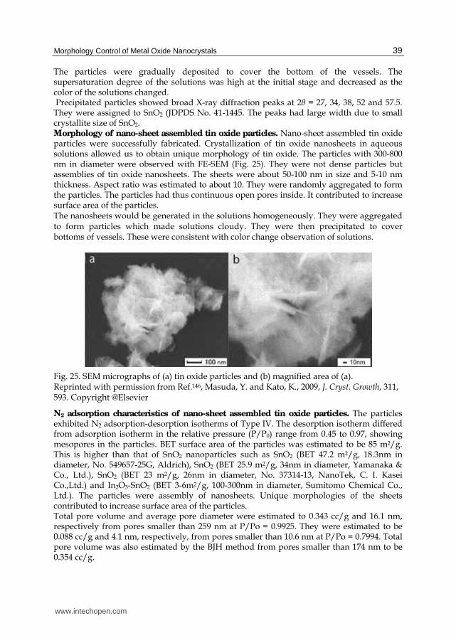
Morphology Control of Metal Oxide Nanocrystals
39
The particles were gradually deposited to cover the bottom of the vessels. The supersaturation degree of the solutions was high at the initial stage and decreased as the color of the solutions changed. Precipitated particles showed broad X-ray diffraction peaks at 2θ = 27, 34, 38, 52 and 57.5. They were assigned to SnO2 (JDPDS No. 41-1445. The peaks had large width due to small crystallite size of SnO2. Morphology of nano-sheet assembled tin oxide particles. Nano-sheet assembled tin oxide particles were successfully fabricated. Crystallization of tin oxide nanosheets in aqueous solutions allowed us to obtain unique morphology of tin oxide. The particles with 300-800 nm in diameter were observed with FE-SEM (Fig. 25). They were not dense particles but assemblies of tin oxide nanosheets. The sheets were about 50-100 nm in size and 5-10 nm thickness. Aspect ratio was estimated to about 10. They were randomly aggregated to form the particles. The particles had thus continuous open pores inside. It contributed to increase surface area of the particles. The nanosheets would be generated in the solutions homogeneously. They were aggregated to form particles which made solutions cloudy. They were then precipitated to cover bottoms of vessels. These were consistent with color change observation of solutions.
Fig. 25. SEM micrographs of (a) tin oxide particles and (b) magnified area of (a). Reprinted with permission from Ref.146, Masuda, Y. and Kato, K., 2009, J. Cryst. Growth, 311, 593. Copyright @Elsevier
N2 adsorption characteristics of nano-sheet assembled tin oxide particles. The particles exhibited N2 adsorption-desorption isotherms of Type IV. The desorption isotherm differed from adsorption isotherm in the relative pressure (P/P0) range from 0.45 to 0.97, showing mesopores in the particles. BET surface area of the particles was estimated to be 85 m2/g. This is higher than that of SnO2 nanoparticles such as SnO2 (BET 47.2 m2/g, 18.3nm in diameter, No. 549657-25G, Aldrich), SnO2 (BET 25.9 m2/g, 34nm in diameter, Yamanaka & Co., Ltd.), SnO2 (BET 23 m2/g, 26nm in diameter, No. 37314-13, NanoTek, C. I. Kasei Co.,Ltd.) and In2O3-SnO2 (BET 3-6m2/g, 100-300nm in diameter, Sumitomo Chemical Co., Ltd.). The particles were assembly of nanosheets. Unique morphologies of the sheets contributed to increase surface area of the particles. Total pore volume and average pore diameter were estimated to 0.343 cc/g and 16.1 nm, respectively from pores smaller than 259 nm at P/Po = 0.9925. They were estimated to be 0.088 cc/g and 4.1 nm, respectively, from pores smaller than 10.6 nm at P/Po = 0.7994. Total pore volume was also estimated by the BJH method from pores smaller than 174 nm to be 0.354 cc/g.
www.intechopen.com

Nanocrystal
40
Pore size distribution was calculated by the BJH method using desorption braches. It showed a pore size distribution curve having a strong peak at ~3.9 nm and a broad peak from 25 nm to 175 nm. The particles would have a large amount of mesopores with ~3.9 nm in diameter and mesopores with 25-175 nm in diameter. The pores were spaces surrounded by nanosheets and interparticle spaces. Micropores smaller than 2 nm were not suggested by BJH pore size distribution. In this section, nanosheet assembled tin oxide particles were fabricated by aqueous solution synthesis. Anisotropic crystal growth of tin oxide was effectively utilized to form nanosheet assembled structure. They were crystallized at ordinary temperature without annealing. It allowed us to avoid aggregation of the particles and decrease of surface area. The particles were 300-800 nm in diameter and were crystals of SnO2 and SnO. The sheets were about 50-100 nm in size and 5-10 nm thickness. The particles had BET surface area of 85 m2/g estimated with N2 adsorption characteristics. BJH analysis indicated that mesopores of 3.9 nm in size contributed to increase surface area. The particles were prepared by environmentally friendly process. The system had advantages on low cost, low energy consumption and low CO2 emission.
9. Enhancement of surface area of tin oxide180
Tin oxide nano-crystals with high surface area were firstly synthesized in aqueous solutions at 50°C. BET surface area was successfully reached to 194 m2/g180. It was much higher than that of SnO2 (BET 47.2 m2/g, Aldrich), SnO2 (BET 25.9 m2/g, Yamanaka & Co., Ltd.), SnO2 (BET 23 m2/g, C. I. Kasei Co.,Ltd.) and In2O3-SnO2 (BET 3-6m2/g, Sumitomo Chemical Co., Ltd.). N2 adsorption characteristics revealed that they had pores of 1-3 nm which contributed high surface area. TEM, ED and XRD indicated morphology, crystal structure and chemical composition of nano-crystals. Novel process allowed us to avoid sintering and deformation of the crystals and hence, realized high surface area and unique morphology. In this study, tin oxide nanosheets were formed in the solutions. BET surface area was successfully reached to 194 m2/g. Origin of high surface area was discussed with pore size distribution and morphology observations. Synthesis of tin oxide nanosheets. SnF2 (870.6 mg) was dissolved in distilled water (200 mL) of 50°C to be 5 mM. The solutions were kept at 50°C for 20 min and then at 28°C for 3 days without stirring. The nanocrystals precipitated to cover bottom of the vessels. For comparison, the solutions were centrifuged at 4000 rpm for 10 minafter keeping at 50°C for 20 min. Precipitated particles were dried at 60°C for 12 h after removal of supernatant solutions.
Morphology and crystal phase of tin oxide nanosheets.
The nanosheets synthesized at 50°C for 20min and at 28°C for 3 days were mixture of SnO2 main phase and SnO additional phase (Fig. 26a). X-ray diffraction peaks at 2θ = 26.5, 33, 51.4, 62, 64.5, 80 and 89 were assigned to 110, 101, 211, etc. of SnO2 (JDPDS No. 41-1445). 101, 110 and 002 diffraction peaks of SnO (JDPDS No. 06-0395) were over lapped to peaks of
SnO2. For comparison, diffraction pattern of the nanosheets synthesized at 50°C for 20min was shown in Fig. 26b. Half maximum full-width of the peaks was smaller than that in Fig. 26a. Lower SnO content resulted sharp peaks of SnO2 in Fig. 26b. These observations indicated that SnO was mainly formed at 28°C rather than at 50°C. The nanosheets were well dispersed in ethanol. The nanosheets in supernatant solutions were skimmed with Cu grids for TEM observations. They were 20-50 nm in diameter having
www.intechopen.com
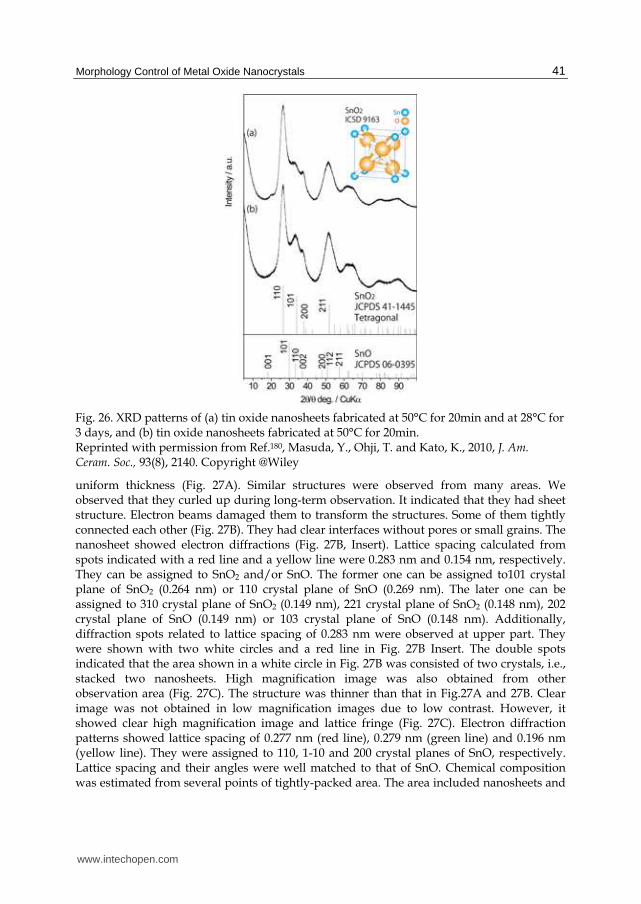
Morphology Control of Metal Oxide Nanocrystals
41
Fig. 26. XRD patterns of (a) tin oxide nanosheets fabricated at 50°C for 20min and at 28°C for 3 days, and (b) tin oxide nanosheets fabricated at 50°C for 20min. Reprinted with permission from Ref.180, Masuda, Y., Ohji, T. and Kato, K., 2010, J. Am. Ceram. Soc., 93(8), 2140. Copyright @Wiley
uniform thickness (Fig. 27A). Similar structures were observed from many areas. We observed that they curled up during long-term observation. It indicated that they had sheet structure. Electron beams damaged them to transform the structures. Some of them tightly connected each other (Fig. 27B). They had clear interfaces without pores or small grains. The nanosheet showed electron diffractions (Fig. 27B, Insert). Lattice spacing calculated from spots indicated with a red line and a yellow line were 0.283 nm and 0.154 nm, respectively. They can be assigned to SnO2 and/or SnO. The former one can be assigned to101 crystal plane of SnO2 (0.264 nm) or 110 crystal plane of SnO (0.269 nm). The later one can be assigned to 310 crystal plane of SnO2 (0.149 nm), 221 crystal plane of SnO2 (0.148 nm), 202 crystal plane of SnO (0.149 nm) or 103 crystal plane of SnO (0.148 nm). Additionally, diffraction spots related to lattice spacing of 0.283 nm were observed at upper part. They were shown with two white circles and a red line in Fig. 27B Insert. The double spots indicated that the area shown in a white circle in Fig. 27B was consisted of two crystals, i.e., stacked two nanosheets. High magnification image was also obtained from other observation area (Fig. 27C). The structure was thinner than that in Fig.27A and 27B. Clear image was not obtained in low magnification images due to low contrast. However, it showed clear high magnification image and lattice fringe (Fig. 27C). Electron diffraction patterns showed lattice spacing of 0.277 nm (red line), 0.279 nm (green line) and 0.196 nm (yellow line). They were assigned to 110, 1-10 and 200 crystal planes of SnO, respectively. Lattice spacing and their angles were well matched to that of SnO. Chemical composition was estimated from several points of tightly-packed area. The area included nanosheets and
www.intechopen.com

Nanocrystal
42
spherical crystals. Chemical composition varied among each positions in the range of Sn : O = 1 : 1.7-2.7 which was similar to that of SnO2 rather than SnO. These observations indicated that the crystals were mixture of SnO2 and SnO.
Fig. 27. TEM micrographs and electron diffraction patterns of tin oxide nanosheets. (b): high magnification image of (a). (c): high magnification image of other area. Reprinted with permission from Ref.180, Masuda, Y., Ohji, T. and Kato, K., 2010, J. Am. Ceram. Soc., 93(8), 2140. Copyright @Wiley
N2 adsorption characteristics of tin oxide nanosheets.
BET surface area of the nanosheets was estimated from N2 adsorption isotherm (Fig. 28a). The nanosheets had successfully high surface area of 194 m2/g (Fig. 28b). It was much higher than that of SnO2 nanoparticles such as SnO2 (BET 47.2 m2/g, 18.3nm in diameter, No. 549657-25G, Aldrich), SnO2 (BET 25.9 m2/g, 34nm in diameter, Yamanaka & Co., Ltd., Osaka, Japan), SnO2 (BET 23 m2/g, 26nm in diameter, No. 37314-13, NanoTek, C. I. Kasei Co.,Ltd., Tokyo, Japan) and In2O3-SnO2 (BET 3-6m2/g, 100-300nm in diameter, Sumitomo Chemical Co., Ltd.). Additionally, it was more than double higher than that of previous report (85 m2/g)181. Pore size distribution was analyzed with BJH method using adsorption isotherm (Fig. 28c). It indicated that the nanosheets included pores of 1-2 nm. Micropore analysis was performed with DFT/Monte-Carlo Fitting which was completely-consistent
www.intechopen.com

Morphology Control of Metal Oxide Nanocrystals
43
with isotherms (Fig. 28d). Pores of 1-3 nm were shown to be in the nanosheets (Fig. 28e). The micro and meso-pores contributed high surface area of 194 m2/g in this system. For comparison, BET surface area of the nanosheets synthesized at 50°C for 20min was estimated to 146 m2/g. It was also higher than that of nanoparticles in former studies. In this section, nanosheets of tin oxides were fabricated in aqueous solutions at ordinary temperature. BET surface area successfully reached to 194 m2/g. It was much higher than that of nanoparticles in former studies. 2-dimensional sheet structure was one of ideal structures for high surface area per unit weight. Nano sized thickness directly contributed high surface area. Crystalline nanosheets were prepared without high temperature annealing which degraded surface area and nanostructures. High surface area and unique nanostructures of the sheets can be applied to gas sensors, dye-sensitized solar cells and molecular sensors.
Fig. 28. (a): N2 adsorption-desorption isotherm of tin oxide nanosheets. (b): BET surface area of tin oxide nanosheets. (c): Pore size distribution calculated from N2 adsorption data of tin oxide nanosheets using BJH equation. (d): N2 adsorption-desorption isotherm and DFT/Monte-Carlo fitting curve of tin oxide nanosheets. (e): Pore size distribution calculated from N2 adsorption data of tin oxide nanosheets using DFT/Monte-Carlo equation. Reprinted with permission from Ref.180, Masuda, Y., Ohji, T. and Kato, K., 2010, J. Am. Ceram. Soc., 93(8), 2140. Copyright @Wiley
www.intechopen.com

Nanocrystal
44
10. Tin oxide coating on polytetrafluoroethylene films in aqueous solutions182
Tin Polytetrafluoroethylene(PTFE) films were successfully coated with tin oxide in aqueous solutions. Tin oxide was crystallized in the solution and formed nanocrystal coatings on the polymer films. The coatings were consisted of SnO2 and SnO crystals. They were assemblies of tin oxide nanosheet of about 10 nm to 50 nm in size and about 5 nm in thickness. The nanocrystal films can be exfoliated from the PTFE substrates. Tin oxide nanocrystal films had a rough liquid-surface and a dense substrate-side surface. Transparency of PTFE films coated with tin oxide was same to that of bare PTFE films in the range from 400 nm to 800 nm. Tin oxide decreased transparency about 25 % at 320 nm. The PTFE films coated with tin oxide nanocrystals can be pasted on desired substrates. Organic-inorganic hybrid materials such as metal oxide electronics on polymer flexible films have received considerable attention in recent years for light-weight flexible sensors, displays, dye-sensitized solar cells, etc. The polymer films offer the advantages of flexibility, light-weight, low-cost and impact resistance. Tin oxide (SnO2) is an important semiconductor with a wide band gap of 3.6 eV at room temperature. They have been widely used in gas sensors167,183, optical devices147, lithium batteries148-150, etc. A novel type of bio-sensor was proposed to detect environmental toxins such as bisphenol-A or dioxin88,184. Tin oxide is a candidate material for the sensor because
of its suitable band gap, surface characteristics, and high transparency. Metal oxides including tin oxide have been synthesized with high temperature processes at several hundred degrees for many years. Recently, the aqueous syntheses of metal oxides have attracted much attention as a next generation science and technology1,51,114,177. Aqueous systems are environmentally friendly and have advantages of low energy consumption, low cost and an organic solvent free process. In recent years, metal oxide films and their microstructures were fabricated on organic surfaces such as polyethylene terephthalate (PET) films185,186 or self-assembled
monolayers20,113,187,188. However, metal oxide formation on polytetrafluoroethylene (PTFE) was difficult compared to PET films. PTFE films are widely used in electronic applications because of low chemical reactivity, low coefficient of friction, high melting point (327 °C), high-corrosion resistance, a high dielectric strength over many different frequencies, a low
dissipation factor, and a high surface resistivity. They were selected as substrates in this study. In this section, tin oxide nanocrystals were prepared on PTFE films in aqueous
solutions182,184. They were crystallized in the solution containing tin ions to form films consisted of nanosheets. The process realized tin oxide film formation without high temperature annealing and unique morphology of tin oxide crystals.
(1) Aqueous synthesis of tin oxide nanocrystals on PTFE films
SnF2 (870.6 mg) was dissolved in the distilled water (200 mL) at 90°C to be 5 mM. PTFE films (thickness: 50 ┤m, ASF-110, Chukoh) with silicone adhesive (thickness: 30 ┤m) were pasted on quarts substrates (25 × 50 × 1 mm). They were immersed in the middle of the solutions with the bottom up at an angle or with the top up at an angle. They were tilted at 15 degrees
to the upright. The solutions were kept at 90°C using a drying oven (Yamato Scientific Co., Ltd., DKN402) for 2 h with no stirring. The solutions became lightly clouded after 2 h. The as-deposited nanocrystals on substrates were rinsed under running water and dried by a
strong air spray. Additionally, the solutions kept at 90°C for 2 h were centrifuged at 4000
www.intechopen.com
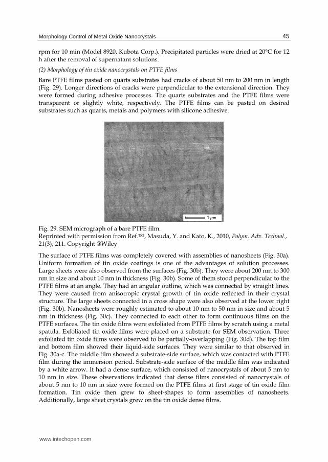
Morphology Control of Metal Oxide Nanocrystals
45
rpm for 10 min (Model 8920, Kubota Corp.). Precipitated particles were dried at 20°C for 12 h after the removal of supernatant solutions.
(2) Morphology of tin oxide nanocrystals on PTFE films
Bare PTFE films pasted on quarts substrates had cracks of about 50 nm to 200 nm in length (Fig. 29). Longer directions of cracks were perpendicular to the extensional direction. They were formed during adhesive processes. The quarts substrates and the PTFE films were transparent or slightly white, respectively. The PTFE films can be pasted on desired substrates such as quarts, metals and polymers with silicone adhesive.
Fig. 29. SEM micrograph of a bare PTFE film. Reprinted with permission from Ref.182, Masuda, Y. and Kato, K., 2010, Polym. Adv. Technol., 21(3), 211. Copyright @Wiley
The surface of PTFE films was completely covered with assemblies of nanosheets (Fig. 30a). Uniform formation of tin oxide coatings is one of the advantages of solution processes. Large sheets were also observed from the surfaces (Fig. 30b). They were about 200 nm to 300 nm in size and about 10 nm in thickness (Fig. 30b). Some of them stood perpendicular to the PTFE films at an angle. They had an angular outline, which was connected by straight lines. They were caused from anisotropic crystal growth of tin oxide reflected in their crystal structure. The large sheets connected in a cross shape were also observed at the lower right (Fig. 30b). Nanosheets were roughly estimated to about 10 nm to 50 nm in size and about 5 nm in thickness (Fig. 30c). They connected to each other to form continuous films on the PTFE surfaces. The tin oxide films were exfoliated from PTFE films by scratch using a metal spatula. Exfoliated tin oxide films were placed on a substrate for SEM observation. Three exfoliated tin oxide films were observed to be partially-overlapping (Fig. 30d). The top film and bottom film showed their liquid-side surfaces. They were similar to that observed in Fig. 30a-c. The middle film showed a substrate-side surface, which was contacted with PTFE film during the immersion period. Substrate-side surface of the middle film was indicated by a white arrow. It had a dense surface, which consisted of nanocrystals of about 5 nm to 10 nm in size. These observations indicated that dense films consisted of nanocrystals of about 5 nm to 10 nm in size were formed on the PTFE films at first stage of tin oxide film formation. Tin oxide then grew to sheet-shapes to form assemblies of nanosheets. Additionally, large sheet crystals grew on the tin oxide dense films.
www.intechopen.com

Nanocrystal
46
Fig. 30. SEM micrographs of (a) tin oxide nanocrystals on a PTFE film and (b, c) magnified area of (a) showing morphology of nanocrystals and (d) exfoliated tin oxide nanocrystal films showing liquid-side surface and substrate-side surface. Substrate-side surface is indicated by a white arrow.
Reprinted with permission from Ref.182, Masuda, Y. and Kato, K., 2010, Polym. Adv. Technol.,
21(3), 211. Copyright @Wiley
(3) Crystal phase of tin oxide nanocrystals on PTFE films
X-ray diffraction pattern obtained from a PTFE film coated with tin oxide was similar to that from a bare PTFE film. Diffraction peaks assigned to tin oxide were not observed because of thin film thickness. Precipitated particles were evaluated after drying. They showed broad X-ray diffraction peaks at 2θ = 27, 34, 38 and 52. They were assigned to 110, 101, 200 or 211 diffraction peaks from SnO2 (JDPDS No. 41-1445) (Fig. 3c). The peaks were wide in width due to the small crystallite size of SnO2. Peaks were also observed 2θ = 29.5, 32.0, 37.4, 48.0, 50.4 and 57.4. They were assigned to 101, 110, 002, 200, 112 or 211 diffraction peaks from SnO (JDPDS No. 06-0395). XRD analysis indicated that the particles obtained from the solutions consisted of SnO2 crystals and SnO crystals.
(4) XPS analysis of tin oxide nanocrystals on PTFE films
Carbon, fluorine and oxygen were detected from bare PTFE films (Fig. 31b). Chemical ratio of them was estimated to C : F : O = 1 : 2.05 : 0.02. It was consistent with chemical composition of polytetrafluoroethylene (PTFE, C : F = 1 : 2). Small amount of oxygen was detected from surface contamination. PTFE films coated with tin oxide showed spectra of tin, oxygen, fluorine and carbon (Fig. 31a). Spectral peak corresponding to Sn 3d5/2 was observed at 487.2 eV (Fig. 31c1). The binding energy was similar to that of SnO2 (486.3 eV189, 486.5 eV190, 486.6 eV191, 487.3 eV) and higher than that of Sn metal (484.8 eV, 484.85 eV,
www.intechopen.com

Morphology Control of Metal Oxide Nanocrystals
47
484.87 eV, 484.9 eV, 485.0 eV), which suggested tin atoms in surface coatings were positively charged by forming direct bonds with oxygen. Binding energy of O 1s centered at about 531.2 eV corresponds to that of SnO2 (Fig. 31c2). Chemical ratio of the coatings was estimated to Sn : O : F : C = 1 : 1.88 : 7.25 : 3.82 and C : F = 1 : 1.90. It was indicated that the surface coatings consisted mainly of SnO2 (Sn : 1 : 2). They were formed on polytetrafluoroethylene films (PTFE, C : F = 1 : 2). Difference and similarity between XPS analyses and XRD analyses suggested deposition mechanism of tin oxides. Crystal phases and chemical compositions of the surface coatings were different from those of the precipitated particles. SnO2 crystallized on the films to form surface coatings, on the other hand, SnO2 and SnO homogeneously crystallized to form particles in the solutions. Pure SnO2 coatings were thus successfully formed on the PTFE films.
Fig. 31. XPS spectra of (a) tin oxide nanocrystals on a PTFE film and (b) a bare PTFE film. (c1) Sn 3d5/2 spectrum and (c2) O 1s spectrum of tin oxide nanocrystals on a PTFE film. Reprinted with permission from Ref.182, Masuda, Y. and Kato, K., 2010, Polym. Adv. Technol., 21(3), 211. Copyright @Wiley
(5) Optical property of tin oxide nanocrystals on PTFE films
Quarts substrates had high transparency in the range from 200 nm to 850 nm (Fig. 32, black line). PTFE films pasted on quarts substrates were visually observed to be slight white. Their transparency was lower than that of quarts (Fig. 32, red line). Especially, it decreased as decrease of wavelength below 350 nm. PTFE films coated with tin oxide showed the same transparency as bare PTFE films in the range from 400 nm to 850 nm (Fig. 32, blue line). They decreased transparency about 25 % at 320 nm. Tin oxide particles precipitated from the solution were evaluated for comparison. They had absorption peak centered at 320 nm. This absorption was caused by tin oxide. These analyses indicated that tin oxide was deposited on PTFE films immersed in the solutions and they decrease transparency at 320 nm.
11. Conclusion
Polytetrafluoroethylene (PTFE) films were successfully coated with tin oxide nanocrystals. Tin oxide was crystallized in aqueous solutions to form nanosheet-assembled films. They were about 10 nm to 50 nm in size and about 5 nm in thickness. Large sheets of about 200 nm to 300 nm in size and about 10 nm in thickness were also crystallized on the surfaces. X-ray diffraction analysis indicated that tin oxide was a mixture of SnO2 and SnO. PTFE films coated with tin oxide were transparent in the range from 400 nm to 850 nm. Tin oxide on the films had absorption centered at 320 nm. Tin oxide coated PTFE films can be pasted on desired substrates. Hybrid tin oxide-PTFE composites may be useful for increasing the potential application of tin oxide film as flexible electronics.
www.intechopen.com

Nanocrystal
48
Fig. 32. UV-Vis spectra of (a) a quarts substrate (black line), (b) a PTFE film pasted on a quarts substrate (red line) and (c) tin oxide nanocrystals on a PTFE film pasted on a quarts substrate (blue line). UV-Vis spectrum of tin oxide particles. Reprinted with permission from Ref.182, Masuda, Y. and Kato, K., 2010, Polym. Adv. Technol., 21(3), 211. Copyright @Wiley
12. Summary
Liquid phase morphology control of metal oxide was developed by precise control of crystal growth in this study. Various nano/micro-structures of them were fabricated in solution systems. These would contribute to development of future metal oxide devices and develop new academic fields.
13. References
[1] Masuda, Y.; Yamada, T.; Koumoto, K. Cryst. Growth Des. 2008, 8, 169-171. [2] Tanaka, K.; Suzuki, K.; Fu, D. S.; Nishizawa, K.; Miki, T.; Kato, K. Jpn. J. Appl. Phys. 2004,
43, 6525-6529. [3] Aoyagi, S.; Kuroiwa, Y.; Sawada, A.; Kawaji, H.; Atake, T. J. Therm. Anal. Cal. 2005, 81,
627-630. [4] Luan, W. L.; Gao, L.; Guo, J. K. Ceram. Inter. 1999, 25, 727-729. [5] Wang, X. H.; Chen, R. Z.; Gui, Z. L.; Li, L. T. Mater. Sci. Eng. B 2003, 99, 199-202. [6] Sakabe, Y.; Yamashita, Y.; Yamamoto, H. J. Euro. Ceram. Soc. 2005, 25, 2739-2742. [7] Polotai, A. V.; Ragulya, A. V.; Randall, C. A. Ferroelectrics 2003, 288, 93-102. [8] Yashima, M.; Hoshina, T.; Ishimura, D.; Kobayashi, S.; Nakamura, W.; Tsurumi, T.;
Wada, S. J. Appl. Phys. 2005, 98. [9] Frey, M. H.; Xu, Z.; Han, P.; Payne, D. A. Ferroelectrics 1998, 206, 337-353. [10] Frey, M. H.; Payne, D. A. Phys. Rev. B 1996, 54, 3158-3168. [11] Wada, S.; Suzuki, T.; Noma, T. J. Ceram. Soc. Japan 1996, 104, 383-392. [12] Masuda, Y.; Koumura, T.; Okawa, T.; Koumoto, K. J. Colloid Interface Sci. 2003, 263, 190-
195. [13] Masuda, Y.; Koumoto, K.; Ueyama, R. Japanese Patent Application Number: P2007-
113579, 2007. [14] Hayashi, Y.; Kimura, T.; Yamaguchi, T. J. Mater. Sci. 1986, 21, 757-762.
www.intechopen.com

Morphology Control of Metal Oxide Nanocrystals
49
[15] Li, X. L.; Liu, J. F.; Li, Y. D. Mater. Chem. Phys. 2003, 80, 222-227. [16] Sun, H.; Kang, S. Z.; Mu, J. Mater. Lett. 2007, 61, 4121-4123. [17] Mutin, J. C.; Dusausoy, Y.; Protas, J. J. Solid State Chem. 1981, 36, 356-364. [18] Potdar, H. S.; Deshpande, S. B.; Date, S. K. J. Am. Ceram. Soc. 1996, 79, 2795-2797. [19] Masuda, Y.; Kinoshita, N.; Koumoto, K. J. Nanosci. Nanotechnol., in press. [20] Masuda, Y.; Kinoshita, N.; Sato, F.; Koumoto, K. Cryst. Growth Des. 2006, 6, 75-78. [21] Wu, X. L.; Siu, G. G.; Fu, C. L.; Ong, H. C. Appl. Phys. Lett. 2001, 78, 2285-2287. [22] Kang, J. S.; Kang, H. S.; Pang, S. S.; Shim, E. S.; Lee, S. Y. Thin Solid Films 2003, 443, 5-8. [23] Golego, N.; Studenikin, S. A.; Cocivera, M. J. J. Electrochem. Soc. 2000, 147, 1592-1594. [24] Sberveglieri, G. Sens. Actuators B: Chem. 1995, 23, 103-109. [25] Pauporte, T.; Lincot, D. Electrochem. Acta. 2000, 45, 3345-3353. [26] Law, M.; Greene, L. E.; Johnson, J. C.; Saykally, R.; Yang, P. D. Nature Mater. 2005, 4, 455-
459. [27] Masuda, Y.; Kato, K. Cryst. Growth Des. 2008, 8, 2633-2637. [28] Gong, H.; Hu, J. Q.; Wang, J. H.; Ong, C. H.; Zhu, F. R. Sens. Actuators B: Chem. 2006, 115,
247-251. [29] Moon, W. J.; Yu, J. H.; Choi, G. M. Sens. Actuators B: Chem. 2002, 87, 464-470. [30] Chang, J. F.; Kuo, H. H.; Leu, I. C.; Hon, M. H. Sens. Actuators B: Chem. 2002, 84, 258-264. [31] Tang, H. X.; Yan, M.; Zhang, H.; Li, S. H.; Ma, X. F.; Wang, M.; Yang, D. R. Sens.
Actuators B: Chem. 2006, 114, 910-915. [32] Shishiyanu, S. T.; Shishiyanu, T. S.; Lupan, O. I. Sens. Actuators B: Chem. 2005, 107, 379-
386. [33] Wagh, M. S.; Patil, L. A.; Seth, T.; Amalnerkar, D. P. Mater. Chem. Phys. 2004, 84, 228-233. [34] Xu, J. Q.; Pan, Q. Y.; Shun, Y. A.; Tian, Z. Z. Sens. Actuators B: Chem. 2000, 66, 277-279. [35] Paraguay, D. F.; Miki-Yoshida, M.; Morales, J.; Solis, J.; Estrada, L. W. Thin Solid Films
2000, 373, 137-140. [36] Baxter, J. B.; Aydil, E. S. Appl. Phys. Lett. 2005, 86, 53114. [37] Katoh, R.; Furube, A.; Hara, K.; Murata, S.; Sugihara, H.; Arakawa, H.; Tachiya, M. J.
Phys. Chem. B 2002, 106, 12957-12964. [38] Karuppuchamy, S.; Nonomura, K.; Yoshida, T.; Sugiura, T.; Minoura, H. Solid State
Ionics 2002, 151, 19-27. [39] Keis, K.; Bauer, C.; Boschloo, G.; Hagfeldt, A.; Westermark, K.; Rensmo, H.; Siegbahn,
H. J. Photochem. Photobiol. A 2002, 148, 57-64. [40] Kasuga, T.; Hiramatsu, M.; Hosono, A.; Sekino, T.; Niihara, K. Adv. Mater. 1999, 11,
1307-+. [41] Oaki, Y.; Imai, H. J. Am. Chem. Soc. 2004, 126, 9271-9275. [42] Xia, Y. N.; Yang, P. D.; Sun, Y. G.; Wu, Y. Y.; Mayers, B.; Gates, B.; Yin, Y. D.; Kim, F.;
Yan, Y. Q. Adv. Mater. 2003, 15, 353-389. [43] Masuda, Y.; Saito, N.; Hoffmann, R.; De Guire, M. R.; Koumoto, K. Sci. Tech. Adv. Mater.
2003, 4, 461-467. [44] Masuda, Y.; Ieda, S.; Koumoto, K. Langmuir 2003, 19, 4415-4419. [45] Masuda, Y.; Jinbo, Y.; Yonezawa, T.; Koumoto, K. Chem. Mater. 2002, 14, 1236-1241. [46] Nakanishi, T.; Masuda, Y.; Koumoto, K. Chem. Mater. 2004, 16, 3484-3488. [47] Peng, W. Q.; Qu, S. C.; Cong, G. W.; Wang, Z. G. Cryst. Growth Des. 2006, 6, 1518-1522. [48] Lin, Y. R.; Yang, S. S.; Tsai, S. Y.; Hsu, H. C.; Wu, S. T.; Chen, I. C. Cryst. Growth Des.
2006, 6, 1951-1955.
www.intechopen.com
Nanocrystal
50
[49] Zhang, H.; Yang, D. R.; Li, D. S.; Ma, X. Y.; Li, S. Z.; Que, D. L. Cryst. Growth Des. 2005, 5, 547-550.
[50] Liu, K. H.; Lin, C. C.; Chen, S. Y. Cryst. Growth Des. 2005, 5, 483-487. [51] Masuda, Y.; Kato, K. Cryst. Growth Des. 2008, 8, 275-279. [52] Greene, L. E.; Law, M.; Tan, D. H.; Montano, M.; Goldberger, J.; Somorjai, G.; Yang, P.
D. Nano Lett. 2005, 5, 1231-1236. [53] O'Brien, P.; Saeed, T.; Knowles, J. J. Mater. Chem. 1996, 6, 1135-1139. [54] Yamabi, S.; Imai, H. J. Mater. Chem. 2002, 12, 3773-3778. [55] Vayssieres, L.; Keis, K.; Lindquist, S. E.; Hagfeldt, A. J. Phys. Chem. B 2001, 105, 3350-
3352. [56] Vayssieres, L. Adv. Mater. 2003, 15, 464-466. [57] Saito, N.; Haneda, H.; Sekiguchi, T.; Ohashi, N.; Sakaguchi, I.; Koumoto, K. Adv. Mater.
2002, 14, 418-421. [58] Saito, N.; Haneda, H.; Seo, W. S.; Koumoto, K. Langmuir 2001, 17, 1461-1469. [59] Saeed, T.; O'Brien, P. Thin Solid Films 1995, 271, 35-38. [60] Kakiuchi, K.; Hosono, E.; Kimura, T.; Imai, H.; Fujihara, S. J. Sol-Gel Sci. Technol. 2006,
39, 63-72. [61] Schwenzer, B.; Gomm, J. R.; Morse, D. E. Langmuir 2006, 22, 9829-9831. [62] Yu, H. D.; Zhang, Z. P.; Han, M. Y.; Hao, X. T.; Zhu, F. R. J. Am. Chem. Soc. 2005, 127,
2378-2379. [63] Choi, K. S.; Lichtenegger, H. C.; Stucky, G. D.; McFarland, E. W. J. Am. Chem. Soc. 2002,
124, 12402-12403. [64] Yin, M.; Gu, Y.; Kuskovsky, I. L.; Andelman, T.; Zhu, Y.; Neumark, G. F.; O'Brien, S. J.
Am. Chem. Soc. 2004, 126, 6206-6207. [65] Feng, X. J.; Feng, L.; Jin, M. H.; Zhai, J.; Jiang, L.; Zhu, D. B. J. Am. Chem. Soc. 2004, 126,
62-63. [66] Yoshida, T.; Tochimoto, M.; Schlettwein, D.; Wohrle, D.; Sugiura, T.; Minoura, H. Chem.
Mater. 1999, 11, 2657-2667. [67] Lee, J. Y.; Yin, D. H.; Horiuchi, S. Chem. Mater. 2005, 17, 5498-5503. [68] Kopalko, K.; Godlewski, M.; Domagala, J. Z.; Lusakowska, E.; Minikayev, R.;
Paszkowicz, W.; Szczerbakow, A. Chem. Mater. 2004, 16, 1447-1450. [69] Turgeman, R.; Gershevitz, O.; Deutsch, M.; Ocko, B. M.; Gedanken, A.; Sukenik, C. N.
Chem. Mater. 2005, 17, 5048-5056. [70] Turgeman, R.; Gershevitz, O.; Palchik, O.; Deutsch, M.; Ocko, B. M.; Gedanken, A.;
Sukenik, C. N. Cryst. Growth Des. 2004, 4, 169-175. [71] Mirica, E.; Kowach, G.; Evans, P.; Du, H. Cryst. Growth Des. 2004, 4, 147-156. [72] Lin, Y. R.; Tseng, Y. K.; Yang, S. S.; Wu, S. T.; Hsu, C. L.; Chang, S. J. Cryst. Growth Des.
2005, 5, 579-583. [73] Gao, Y. F.; Nagai, M. Langmuir 2006, 22, 3936-3940. [74] Wu, X. D.; Zheng, L. J.; Wu, D. Langmuir 2005, 21, 2665-2667. [75] Peterson, R. B.; Fields, C. L.; Gregg, B. A. Langmuir 2004, 20, 5114-5118. [76] Liu, T. Y.; Liao, H. C.; Lin, C. C.; Hu, S. H.; Chen, S. Y. Langmuir 2006, 22, 5804-5809. [77] Masuda, Y.; Kato, K. Cryst. Growth Des. 2008, 8, 3213-3218. [78] Carlson, T.; Giffin, G. L. J. Phys. Chem. 1986, 90, 5896-5900. [79] Zhang, Z. B.; Wang, C. C.; Zakaria, R.; Ying, J. Y. J. Phys. Chem. B 1998, 102, 10871-10878. [80] Wang, R.; Hashimoto, K.; Fujishima, A. Nature 1997, 388, 431-432.
www.intechopen.com

Morphology Control of Metal Oxide Nanocrystals
51
[81] Choi, W. Y.; Termin, A.; Hoffmann, M. R. J. Phys. Chem. 1994, 98, 13669-13679. [82] Sung, Y. M.; Lee, J. K.; Chae, W. S. Cryst. Growth Des. 2006, 6, 805-808. [83] Kumazawa, N.; Islam, M. R.; Takeuchi, M. J. Electroanal. Chem. 1999, 472, 137-141. [84] Ferroni, M.; Carotta, M. C.; Guidi, V.; Martinelli, G.; Ronconi, F.; Sacerdoti, M.; Traversa,
E. Sens. Actuators B: Chem. 2001, 77, 163-166. [85] Wagemaker, M.; Kentgens, A. P. M.; Mulder, F. M. Nature 2002, 418, 397-399. [86] Arico, A. S.; Bruce, P.; Scrosati, B.; Tarascon, J. M.; Van Schalkwijk, W. Nature Mater.
2005, 4, 366-377. [87] Guo, Y. G.; Hu, Y. S.; Maier, J. Chem. Commun. 2006, 26, 2783-2785. [88] Tokudome, H.; Yamada, Y.; Sonezaki, S.; Ishikawa, H.; Bekki, M.; Kanehira, K.;
Miyauchi, M. Appl. Phys. Lett. 2005, 87, 213901-213903. [89] Nazeeruddin, M. K.; De Angelis, F.; Fantacci, S.; Selloni, A.; Viscardi, G.; Liska, P.; Ito,
S.; Takeru, B.; Gratzel, M. G. J. Am. Chem. Soc. 2005, 127, 16835-16847. [90] Wang, P.; Zakeeruddin, S. M.; Moser, J. E.; Humphry-Baker, R.; Comte, P.; Aranyos, V.;
Hagfeldt, A.; Nazeeruddin, M. K.; Gratzel, M. Adv. Mater. 2004, 16, 1806-1811. [91] Morrison, P. W.; Raghavan, R.; Timpone, A. J.; Artelt, C. P.; Pratsinis, S. E. Chem. Mater.
1997, 9, 2702-2708. [92] Yang, G. X.; Zhuang, H. R.; Biswas, P. Nanostruct. Mater. 1996, 7, 675-689. [93] Yu, J. C.; Yu, J. G.; Ho, W. K.; Zhang, L. Z. Chem. Commun. 2001, 19, 1942-1943. [94] Huang, W. P.; Tang, X. H.; Wang, Y. Q.; Koltypin, Y.; Gedanken, A. Chem. Commun.
2000, 15, 1415-1416. [95] Seifried, S.; Winterer, M.; Hahn, H. Chem. Vap. Deposition 2000, 6, 239-244. [96] Scolan, E.; Sanchez, C. Chem. Mater. 1998, 10, 3217-3223. [97] Wang, C. C.; Ying, J. Y. Chem. Mater. 1999, 11, 3113-3120. [98] Burnside, S. D.; Shklover, V.; Barbe, C.; Comte, P.; Arendse, F.; Brooks, K.; Gratzel, M.
Chem. Mater. 1998, 10, 2419-2425. [99] Zhang, H. Z.; Finnegan, M.; Banfield, J. F. Nano Lett. 2001, 1, 81-85. [100] Sung, Y. M.; Lee, J. K. Cryst. Growth Des. 2004, 4, 737-742. [101] Perkas, N.; Pol, V.; Pol, S.; Gedanken, A. Cryst. Growth Des. 2006, 6, 293-296. [102] Deki, S.; Aoi, Y.; Hiroi, O.; Kajinami, A. Chem. Lett. 1996, 6, 433-434. [103] Deki, S.; Aoi, Y.; Yanagimoto, H.; Ishii, K.; Akamatsu, K.; Mizuhata, M.; Kajinami, A. J.
Mater. Chem. 1996, 6, 1879-1882. [104] Deki, S.; Aoi, Y.; Asaoka, Y.; Kajinami, A.; Mizuhata, M. J. Mater. Chem. 1997, 7, 733-
736. [105] Kishimoto, H.; Takahama, K.; Hashimoto, N.; Aoi, Y.; Deki, S. J. Mater. Chem. 1998, 8,
2019-2024. [106] Choi, S. Y.; Mamak, M.; Coombs, N.; Chopra, N.; Ozin, G. A. Adv. Func. Mater. 2004,
14, 335-344. [107] Antonelli, D. M.; Ying, J. Y. Angew. Chem., Int. Ed. 1995, 34, 2014-2017. [108] Shibata, H.; Ogura, T.; Mukai, T.; Ohkubo, T.; Sakai, H.; Abe, M. J. Am. Chem. Soc. 2005,
127, 16396-16397. [109] Shibata, H.; Mihara, H.; Mlikai, T.; Ogura, T.; Kohno, H.; Ohkubo, T.; Sakait, H.; Abe,
M. Chem. Mater. 2006, 18, 2256-2260. [110] Tian, B. Z.; Liu, X. Y.; Yang, H. F.; Xie, S. H.; Yu, C. Z.; Tu, B.; Zhao, D. Y. Adv. Mater.
2003, 15, 1370-+. [111] Ryoo, R.; Joo, S. H.; Kruk, M.; Jaroniec, M. Adv. Mater. 2001, 13, 677-681.
www.intechopen.com

Nanocrystal
52
[112] Masuda, Y.; Kato, K. Japan, 2007. [113] Masuda, Y.; Sugiyama, T.; Seo, W. S.; Koumoto, K. Chem. Mater. 2003, 15, 2469-2476. [114] Masuda, Y.; Kato, K. Chem. Mater. 2008, 20, 1057-1063. [115] Furlong, D. N.; Parfitt, G. D. J. Colloid Interface Sci. 1978, 65, 548-554. [116] Wahi, R. K.; Liu, Y. P.; Falkner, J. C.; Colvin, V. L. J. Colloid Interface Sci. 2006, 302, 530-
536. [117] Kruk, M.; Jaroniec, M. Chem. Mater. 2001, 13, 3169-3183. [118] Ravikovitch, P. I.; Odomhnaill, S. C.; Neimark, A. V.; Schuth, F.; Unger, K. K. Langmuir
1995, 11, 4765-4772. [119] Lastoskie, C.; Gubbins, K. E.; Quirke, N. J. Phys. Chem. 1993, 97, 4786-4796. [120] Katagiri, K.; Ohno, K.; Masuda, Y.; Koumoto, K. J. Ceram. Soc. Japan 2007, 115, 831-834. [121] Masuda, Y.; Ohji, T.; Kato, K. Crystal Growth & Design 2010, 10, 913-922. [122] Masuda, Y.; Kato, K. Thin Solid Films 2008, 516, 2547-2552. [123] Masuda, Y.; Kato, K. J. Cryst. Growth 2009, 311, 512-517. [124] Ohsaka, T.; Izumi, F.; Fujiki, Y. J. Raman Spectrosc. 1978, 7, 321-324. [125] Gao, K. Physica Status Solidi B-Basic Solid State Physics 2007, 244, 2597-2604. [126] Cong, Y.; Zhang, J.; Chen, F.; Anpo, M. J. Phys. Chem. C 2007, 111, 6976-6982. [127] Ohsaka, T.; Yamaoka, S.; Shimomura Solid State Communications 1979, 30, 345-347. [128] Yu, J. G.; Yu, H. G.; Cheng, B.; Zhao, X. J.; Yu, J. C.; Ho, W. K. Journal of Physical
Chemistry B 2003, 107, 13871-13879. [129] Ignat'eva, L. N.; Polishchuk, S. A.; Antokhina, T. F.; Buznik, V. T. Glass Physics and
Chemistry 2004, 30, 139-141. [130] Nakamoto, K. Infrared Spectra of Inorganic and Coordination Compounds; Wiley: New
York, 1970. [131] Padmanabhan, S. C.; Pillai, S. C.; Colreavy, J.; Balakrishnan, S.; McCormack, D. E.;
Perova, T. S.; Gun'ko, Y.; Hinder, S. J.; Kelly, J. M. Chemistry of Materials 2007, 19, 4474-4481.
[132] Wu, J. J.; Yu, C. C. Journal of Physical Chemistry B 2004, 108, 3377-3379. [133] Perathoner, S.; Passalacqua, R.; Centi, G.; S. Su, D.; Weinberg, G. Catalysis Today 2007,
122, 3-13. [134] Sato, H.; Ono, K.; Sasaki, T.; Yamagishi, A. Journal of Physical Chemistry B 2003, 107,
9824-9828. [135] Naik, V. M.; Haddad, D.; Naik, R.; Benci, J.; Auner, G. W. In Symposium on Solid-State
Chemistry of Inorganic Materials IV held at the 2002 MRS Fall Meeting; AlarioFranco, M. A., Greenblatt, M., Rohrer, G., Whittingham, M. S., Eds.; Materials Research Society: Boston, Ma, 2002, p 413-418.
[136] Masuda, Y.; Sugiyama, T.; Lin, H.; Seo, W. S.; Koumoto, K. Thin Solid Films 2001, 382, 153-157.
[137] Huang, D.; Xiao, Z.-D.; Gu, J.-H.; Huang, N.-P.; Yuan, C.-W. Thin Solid Films 1997, 305, 110-115.
[138] Zhang, F.; Mao, Y.; Zheng, Z.; Chen, Y.; Liu, X.; Jin, S. Thin Solid Films 1997, 310, 29-33. [139] Li, D.; Haneda, H.; Hishita, S.; Ohashi, N.; Labhsetwar, N. K. Journal of Fluorine
Chemistry 2005, 126, 69-77. [140] Wang, C. M.; Mallouk, T. E. Journal of Physical Chemistry 1990, 94, 423-428. [141] Minero, C.; Mariella, G.; Maurino, V.; Pelizzetti, E. Langmuir 2000, 16, 2632-2641.
www.intechopen.com

Morphology Control of Metal Oxide Nanocrystals
53
[142] Minero, C.; Mariella, G.; Maurino, V.; Vione, D.; Pelizzetti, E. Langmuir 2000, 16, 8964-8972.
[143] Vohra, M. S.; Kim, S.; Choi, W. In International Symposium on Photochemistry at Interfaces; Elsevier Science Sa: Sapporo, Japan, 2002, p 55-60.
[144] Fu, H. B.; Zhang, L. W.; Zhang, S. C.; Zhu, Y. F.; Zhao, J. C. Journal of Physical Chemistry B 2006, 110, 3061-3065.
[145] Irie, H.; Watanabe, Y.; Hashimoto, K. Journal of Physical Chemistry B 2003, 107, 5483-5486.
[146] Masuda, Y.; Kato, K. J. Cryst. Growth 2009, 311, 593-596. [147] Ginley, D. S.; Bright, C. MRS Bull. 2000, 25, 15-21. [148] Idota, Y.; Kubota, T.; Matsufuji, A.; Maekawa, Y.; Miyasaka, T. Science 1997, 276, 1395 -
1397. [149] Zhang, Y. L.; Liu, Y.; Liu, M. L. Chem. Mater. 2006, 18, 4643-4646. [150] Wang, Y.; Lee, J. Y.; Zeng, H. C. Chem. Mater. 2005, 17, 3899-3903. [151] Bose, A. C.; Kalpana, D.; Thangadurai, P.; Ramasamy, S. Journal of Power Sources 2002,
107, 138-141. [152] Pianaro, S. A.; Bueno, P. R.; Longo, E.; Varela, J., A. J. Mat. Sci. Lett. 1995, 14, 692-694. [153] Bueno, P. R.; de Cassia-Santos, M. R.; Leite, E. R.; Longo, E.; Bisquert, J.; Garcia-
Belmonte, G.; Fabregat-Santiago, F. Journal of Applied Physics 2000, 88, 6545-6548. [154] Tagawa, T.; Kataoka, S.; Hattori, T.; Murakami, Y. Applied Catalysis 1982, 4, 1-4. [155] Park, P. W.; Kung, H. H.; Kim, D. W.; Kung, M. C. Journal of Catalysis 1999, 184, 440-
454. [156] Chopra, K. L.; Major, S.; Pandya, D. K. Thin Solid Films 1983, 102, 1-46. [157] Sergent, N.; Gelin, P.; Perier-Camby, L.; Praliaud, H.; Thomas, G. Sensors and Actuators
B-Chemical 2002, 84, 176-188. [158] Baik, N. S.; Sakai, G.; Miura, N.; Yamazoe, N. J. Am. Ceram. Soc. 2000, 83, 2983-2987. [159] Ristic, M.; Ivanda, M.; Popovic, S.; Music, S. Journal of Non-Crystalline Solids 2002, 303,
270-280. [160] Broussous, L.; Santilli, C. V.; Pulcinelli, S. H.; Craievich, A. F. Journal of Physical
Chemistry B 2002, 106, 2855-2860. [161] Zhang, J. R.; Gao, L. Journal of Solid State Chemistry 2004, 177, 1425-1430. [162] Deng, Z. X.; Wang, C.; Li, Y. D. Journal of The American Ceramic Society 2002, 85, 2837-
2839. [163] Leite, E. R.; Gomes, J. W.; Oliveira, M. M.; Lee, E. J. H.; Longo, E.; Varela, J. A.;
Paskocimas, C. A.; Boschi, T. M.; Lanciotti, F.; Pizani, P. S.; Soares, P. C. Journal of Nanoscience and Nanotechnology 2002, 2, 125-128.
[164] Leite, E. R.; Maciel, A. P.; Weber, I. T.; Lisboa, P. N.; Longo, E.; Paiva-Santos, C. O.; Andrade, A. V. C.; Pakoscimas, C. A.; Maniette, Y.; Schreiner, W. H. Advanced Materials 2002, 14, 905-908.
[165] Dai, Z. R.; Gole, J. L.; Stout, J. D.; Wang, Z. L. J. Phys. Chem. B 2002, 106, 1274 -1279. [166] Liu, Y.; Liu, M. L. Adv. Funct. Mater. 2005, 15, 57 - 62. [167] Huang, J.; Matsunaga, N.; Shimanoe, K.; Yamazoe, N.; Kunitake, T. Chem. Mater. 2005,
17, 3513-3518. [168] Liu, Y. K.; Zheng, C. L.; Wang, W. Z.; Yin, C. R.; Wang, G. H. Adv. Mater. 2001, 13, 1883
- 1887.
www.intechopen.com

Nanocrystal
54
[169] Sun, J. Q.; Wang, J. S.; Wu, X. C.; Zhang, G. S.; Wei, J. Y.; Zhang, S. Q.; Li, H.; Chen, D. R. Cryst. Growth Des. 2006, 6, 1584-1587.
[170] Yang, R. S.; Wang, Z. L. J. Am. Chem. Soc. 2006, 128, 1466-1467. [171] Duan, J. H.; Yang, S. G.; Liu, H. W.; Gong, J. F.; Huang, H. B.; Zhao, X. N.; Zhang, R.;
Du, Y. W. J. Am. Chem. Soc. 2005, 127, 6180 -6181. [172] Ohgi, H.; Maeda, T.; Hosono, E.; Fujihara, S.; Imai, H. Cryst. Growth Des. 2005, 5, 1079-
1083. [173] Uchiyama, H.; Imai, H. Cryst. Growth Des. 2007, 7, 841-843. [174] Niesz, D. E.; Bennett, R. B.; Snyder, M. J. Am. Ceram. Soc. Bull. 1972, 51, 677-680. [175] Roosen, A.; Hausener, H. Adv. Ceram. Mater. 1988, 3, 131. [176] Vasylkiv, O.; Sakka, Y. Journal of The American Ceramic Society 2001, 84, 2489-2494. [177] Niesen, T. P.; DeGuire, M. R. J. Electroceramics 2001, 6, 169-207. [178] Baes, C. F.; Mesiner, R. E. The Hydrolysis of Cations; John Wiley & Sons, Inc., Wiley-
Interscience: New York, 1976. [179] Ararat Ibarguena, C.; Mosqueraa, A.; Parrab, R.; Castrob, M. S.; Rodríguez-Páeza, J. E.
Mater. Chem. Phys. 2007, 101, 433-440. [180] Masuda, Y.; Ohji, T.; Kato, K. Journal of The American Ceramic Society 2010, 93, 2140-
2143. [181] Masuda, Y.; Kato, K. Journal of Crystal Growth 2009, 311, 593-596. [182] Masuda, Y.; Kato, K. Polymers for Advanced Technologies 2010, 21, 211-215. [183] Shukla, S.; Seal, S.; Ludwig, L.; Parish, C. Sens. Actuators B: Chem. 2004, 97, 256-265. [184] Masuda, Y.; Kato, K.; Sonezaki, S.; Ajimi, M.; Bekki, M. Japan, 2008, p P 2008-227389. [185] Xiang, J. H.; Masuda, Y.; Koumoto, K. Adv. Mater. 2004, 16, 1461-1464. [186] Xiang, J. H.; Zhu, P. X.; Masuda, Y.; Koumoto, K. Langmuir 2004, 20, 3278-3283. [187] Masuda, Y.; Yamagishi, M.; Koumoto, K. Chem. Mater. 2007, 19, 1002-1008. [188] Masuda, Y.; Wakamatsu, S.; Koumoto, K. J. Euro. Ceram. Soc. 2004, 24, 301-307. [189] Themlin, J. M.; Chtaib, M.; Henrard, L.; Lambin, P.; Darville, J.; Gilles, J. M. Phys. Rev. B
1992 46, 2460-2466. [190] Yan, L.; Pan, J. S.; Ong, C. K. Mater. Sci. Eng. B 2006, 128, 34-36. [191] Wagner, C. D. Practical Surface Analysis; 2 ed.; John Wiley, 1990; Vol. 1.
www.intechopen.com

NanocrystalEdited by Dr. Yoshitake Masuda
ISBN 978-953-307-199-2Hard cover, 494 pagesPublisher InTechPublished online 28, June, 2011Published in print edition June, 2011
InTech EuropeUniversity Campus STeP Ri Slavka Krautzeka 83/A 51000 Rijeka, Croatia Phone: +385 (51) 770 447 Fax: +385 (51) 686 166www.intechopen.com
InTech ChinaUnit 405, Office Block, Hotel Equatorial Shanghai No.65, Yan An Road (West), Shanghai, 200040, China
Phone: +86-21-62489820 Fax: +86-21-62489821
We focused on cutting-edge science and technology of Nanocrystals in this book. “Nanocrystal†isexpected to lead to the creation of new materials with revolutionary properties and functions. It will open upfresh possibilities for the solution to the environmental problems and energy problems. We wish that this bookcontributes to bequeath a beautiful environment and valuable resources to subsequent generations.
How to referenceIn order to correctly reference this scholarly work, feel free to copy and paste the following:
Yoshitake Masuda (2011). Morphology Control of Metal Oxide Nanocrystals, Nanocrystal, Dr. YoshitakeMasuda (Ed.), ISBN: 978-953-307-199-2, InTech, Available from:http://www.intechopen.com/books/nanocrystal/morphology-control-of-metal-oxide-nanocrystals

© 2011 The Author(s). Licensee IntechOpen. This chapter is distributedunder the terms of the Creative Commons Attribution-NonCommercial-ShareAlike-3.0 License, which permits use, distribution and reproduction fornon-commercial purposes, provided the original is properly cited andderivative works building on this content are distributed under the samelicense.