module 5 logic diagrams - ntc sites textbooks/08... · engineering symbology, prints, &...
TRANSCRIPT
ENGINEERING SYMBOLOGY, PRINTS, AND DRAWINGS
Module 5
Logic Diagrams

Engineering Symbology, Prints, & Drawings Logic Diagrams
i
TABLE OF CONTENTS
Table of Co nte nts
TABLE OF CONTENTS ................................................................................................... i
LIST OF FIGURES ...........................................................................................................ii
LIST OF TABLES ............................................................................................................ iii
REFERENCES ................................................................................................................iv
OBJECTIVES .................................................................................................................. v
ENGINEERING LOGIC DIAGRAMS ............................................................................... 1
Introduction .................................................................................................................. 1
Symbology ................................................................................................................... 4
Time Delays ................................................................................................................. 6
Complex Logic Devices ............................................................................................... 8
Summary ................................................................................................................... 10
TRUTH TABLES AND EXERCISES ............................................................................. 11
Truth Tables .............................................................................................................. 11
Reading Logic Diagrams ........................................................................................... 13
Examples ................................................................................................................... 13
Example 1 .................................................................................................................. 14
Example 2 .................................................................................................................. 16
Summary ................................................................................................................... 20
Engineering Symbology, Prints, & Drawings Logic Diagrams
ii
LIST OF FIGURES
Figure 1 Example of a Pump Start Circuit Schematic Diagram ..................................... 2
Figure 2 Example of Pump Start Circuit as a Logic Diagram ........................................ 3
Figure 3 Basic Logic Symbols ....................................................................................... 5
Figure 4 Conventions for Depicting Multiple Inputs ....................................................... 5
Figure 5 COINCIDENCE Gate ...................................................................................... 6
Figure 6 EXCLUSIVE OR and EXCLUSIVE NOR Gates .............................................. 6
Figure 7 Type One Time Delay Device ......................................................................... 7
Figure 8 Type Two Time Delay Device ......................................................................... 7
Figure 9 Type Three Time Delay Device ....................................................................... 8
Figure 10 Symbols for Complex Logic Devices ............................................................. 9
Figure 11 Truth Tables ................................................................................................ 12
Figure 12 Logic Gate Status Notation ......................................................................... 13
Figure 13 Example 1 ................................................................................................... 14
Figure 14 Example 2 ................................................................................................... 16

Engineering Symbology, Prints, & Drawings Logic Diagrams
iii
LIST OF TABLES
NONE
Engineering Symbology, Prints, & Drawings Logic Diagrams
iv
REFERENCES
ASME Y14.5-2009, Dimensioning and Tolerancing.
IEEE Std 315-1975 (Reaffirmed 1993), Graphic Symbols for Electrical and
Electronic Diagrams.
Gasperini, Richard E., Digital Troubleshooting, Movonics Company; Los Altos,
California, 1976.
Jensen - Helsel, Engineering Drawing and Design, 7th Ed., McGraw-Hill Book
Company, New York (August 15, 2007).
Lenk, John D., Handbook of Logic Circuits, Reston Publishing Company, Reston,
Virginia, 1972.
Wickes, William E., Logic Design with Integrated Circuits, John Wiley & Sons,
Inc, 1968.
Naval Auxiliary Machinery United States Naval Institute, Annapolis, Maryland,
1951.
TPC Training Systems, Reading Schematics and Symbols, Technical Publishing
Company, Barrington, Illinois, 1974.
Arnell, Alvin, Standard Graphical Symbols, McGraw-Hill Book Company, 1963.
George Masche, Systems Summary of a Westinghouse Pressurized Water
Reactor, Westinghouse Electric Corporation, 1971.
Smith-Zappe, Valve Selection Handbook, 5th Ed., Gulf Publishing Company,
Houston, Texas, December 2003.
Engineering Symbology, Prints, & Drawings Logic Diagrams
v
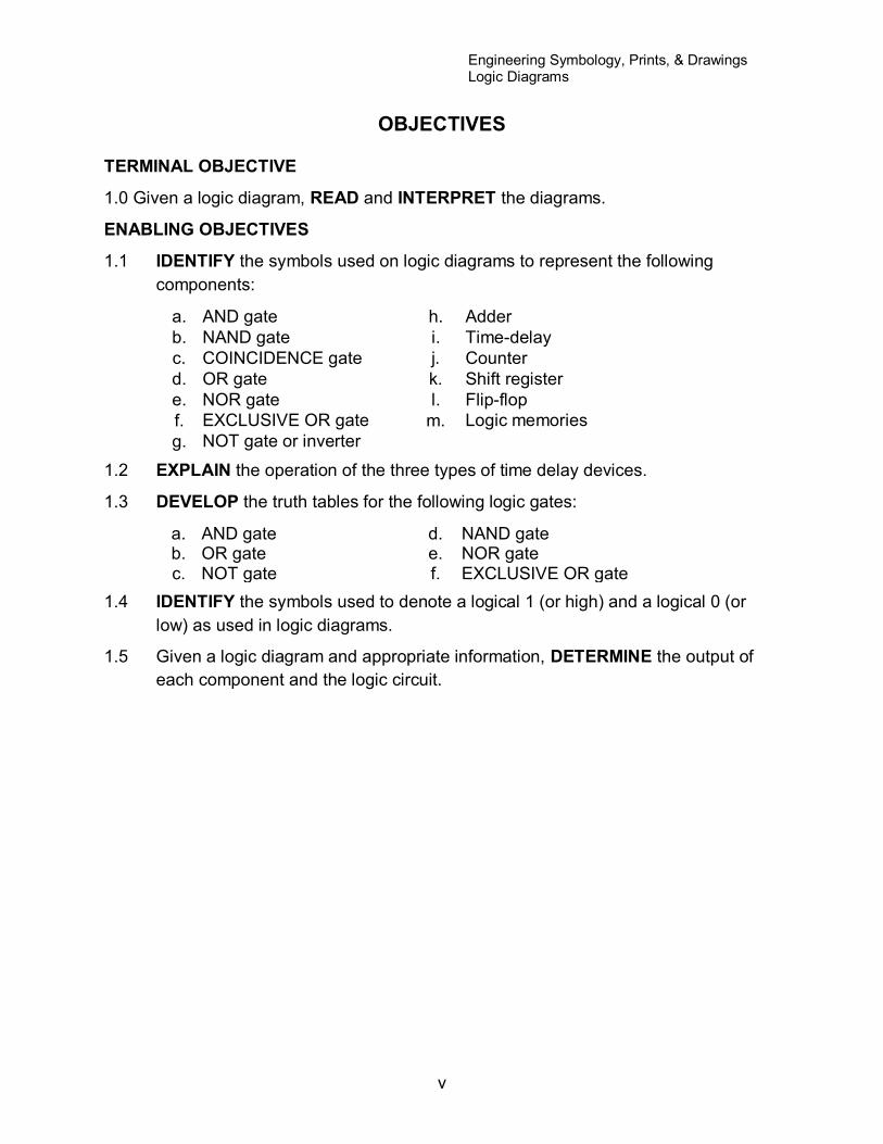
OBJECTIVES
TERMINAL OBJECTIVE
1.0 Given a logic diagram, READ and INTERPRET the diagrams.
ENABLING OBJECTIVES
1.1 IDENTIFY the symbols used on logic diagrams to represent the following
components:
a. AND gate h. Adder
b. NAND gate i. Time-delay
c. COINCIDENCE gate j. Counter
d. OR gate k. Shift register
e. NOR gate l. Flip-flop
f. EXCLUSIVE OR gate m. Logic memories
g. NOT gate or inverter
1.2 EXPLAIN the operation of the three types of time delay devices.
1.3 DEVELOP the truth tables for the following logic gates:
a. AND gate d. NAND gate b. OR gate e. NOR gate c. NOT gate f. EXCLUSIVE OR gate
1.4 IDENTIFY the symbols used to denote a logical 1 (or high) and a logical 0 (or
low) as used in logic diagrams.
1.5 Given a logic diagram and appropriate information, DETERMINE the output of
each component and the logic circuit.
Engineering Symbology, Prints, & Drawings Logic Diagrams
1
ENGINEERING LOGIC DIAGRAMS
This chapter will review the symbols and conventions used on logic diagrams.
EO 1.1 IDENTIFY the symbols used on logic diagrams to represent the
following components:
a. AND gate h. Adder
b. NAND gate i. Time-delay
c. COINCIDENCE gate j. Counter
d. OR gate k. Shift register
e. NOR gate l. Flip-flop
f. EXCLUSIVE OR gate m. Logic memories
g. NOT gate or inverter
EO 1.2 EXPLAIN the operation of the three types of time delay devices.
Introduction
Logic diagrams have many uses. In the solid state industry, they are used as the
principal diagram for the design of solid state components such as computer chips.
They are used by mathematicians to help solve logical problems (called boolean
algebra). However, their principle application at DOE facilities is their ability to present
component and system operational information. The use of logic symbology results in a
diagram that allows the user to determine the operation of a given component or system
as the various input signals change.
To read and interpret logic diagrams, the reader must understand what each of the
specialized symbols represent. This chapter discusses the common symbols used on
logic diagrams. When mastered, this knowledge should enable the reader to understand
most logic diagrams.
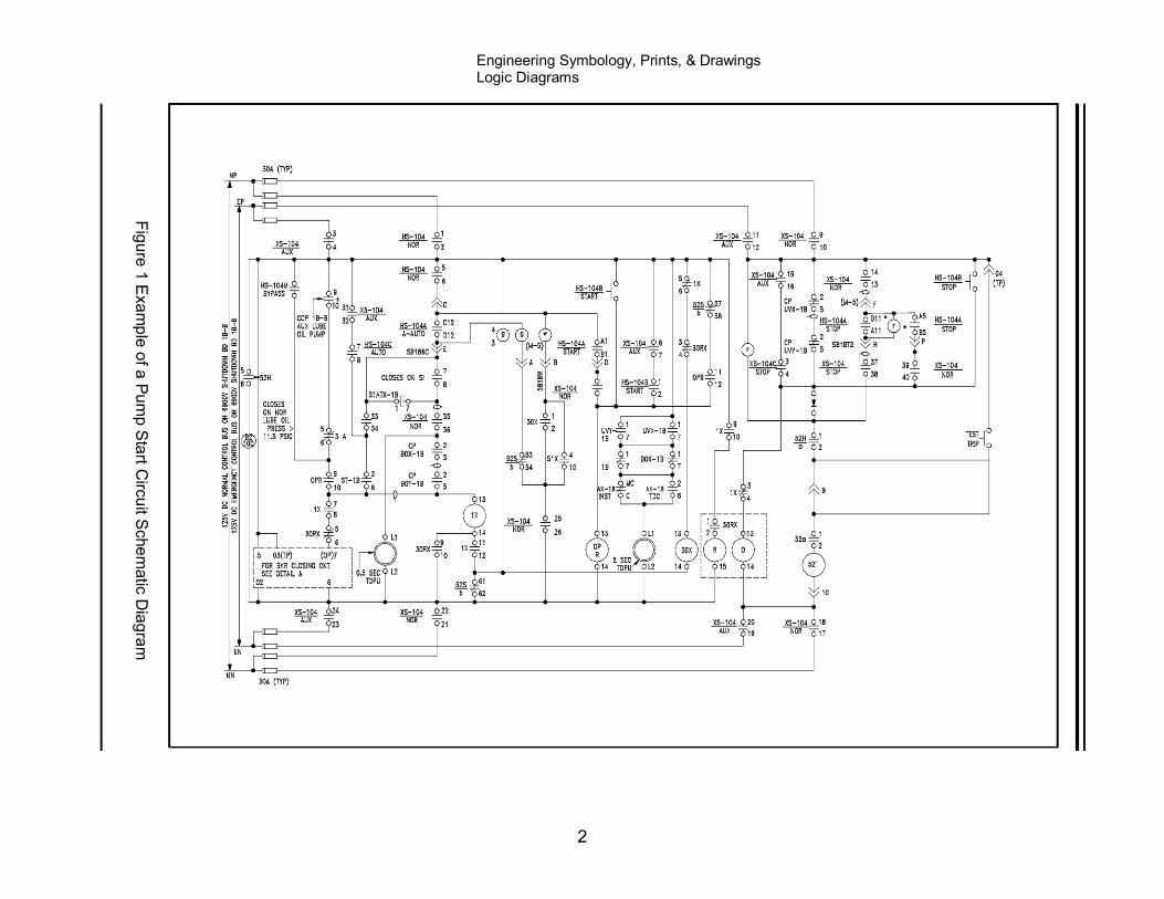
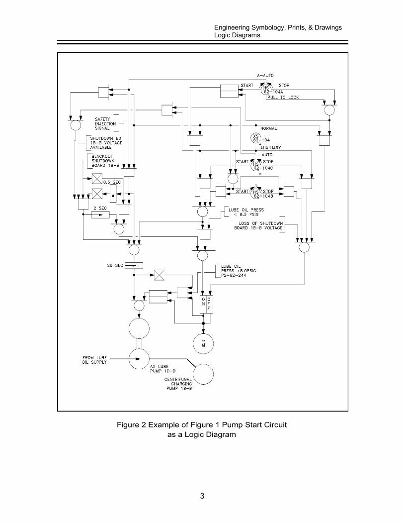
Facility operators and technical staff personnel commonly see logic symbols on
equipment diagrams. The logic symbols, called gates, depict the operation/start/stop
circuits of components and systems. The following two figures, which use a common
facility start/stop pump circuit as an example, clearly demonstrate the reasons for
learning to read logic diagrams. Figure 1 presents a schematic for a large pump, and
Figure 2 shows the same pump circuit using only logic gates. It is obvious that when the
basic logic symbols are understood, figuring out how the pump operates and how it will
respond to various combinations of inputs using the logic diagram is fast and easy, as
compared to laboriously tracing through the relays and contacts of the schematic
diagram for the same information.
Engineering Symbology, Prints, & Drawings Logic Diagrams
2
Fig
ure
1 E
xa
mp
le o
f a P
um
p S
tart C
ircu
it Sche
matic
Dia
gra
m
Engineering Symbology, Prints, & Drawings Logic Diagrams
3
Figure 2 Example of Figure 1 Pump Start Circuit
as a Logic Diagram

Engineering Symbology, Prints, & Drawings Logic Diagrams
4
Symbology
There are three basic types of logic gates. They are AND, OR, and NOT gates. Each
gate is a very simple device that only has two states, on and off. The states of a gate
are also commonly referred to as high or low, 1 or 0, or True or False, where on = high
= 1 = True, and off = low = 0 = False. The state of the gate, also referred to as its
output, is determined by the status of the inputs to the gate, with each type of gate
responding differently to the various possible combinations of inputs. Specifically, these
combinations are as follows.
AND gate - provides an output (on) when all its inputs are on. When any one of
the inputs is off, the gate's output is off.
OR gate - provides an output (on) when any one or more of its inputs is on. The
gate is off only when all of its inputs are off.
NOT gate - provides a reversal of the input. If the input is on, the output will be
off. If the input is off, the output will be on.
Because the NOT gate is frequently used in conjunction with AND and OR gates,
special symbols have been developed to represent these combinations. The
combination of an AND gate and a NOT gate is called a NAND gate. The combination
of an OR gate with a NOT gate is called a NOR gate.
NAND gate - is the opposite (NOT) of an AND gate's output. It provides an output
(on) except when all the inputs are on.
NOR gate - is the opposite (NOT) of an OR gate's output. It provides an output
only when all inputs are off.
Figure 3 illustrates the symbols covering the three basic logic gates plus NAND and
NOR gates. The IEEE/ANSI symbols are used most often; however, other symbol
conventions are provided on Figure 3 for information.

Engineering Symbology, Prints, & Drawings Logic Diagrams
5
Figure 3 Basic Logic Symbols
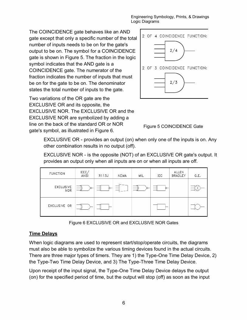
The AND gate has a common variation called a COINCIDENCE gate. Logic gates are
not limited to two inputs. Theoretically, there is no limit to the number of inputs a gate
can have. But, as the number of inputs increases, the symbol must be altered to
accommodate the increased inputs. There are two basic ways to show multiple inputs.
Figure 4 demonstrates both methods, using an OR gate as an example. The symbols
used in Figure 4 are used extensively in computer logic diagrams. Process control logic
diagrams usually use the symbology shown in Figure 2.
Figure 4 Conventions for Depicting Multiple Inputs
Engineering Symbology, Prints, & Drawings Logic Diagrams
6
The COINCIDENCE gate behaves like an AND
gate except that only a specific number of the total
number of inputs needs to be on for the gate's
output to be on. The symbol for a COINCIDENCE
gate is shown in Figure 5. The fraction in the logic
symbol indicates that the AND gate is a
COINCIDENCE gate. The numerator of the
fraction indicates the number of inputs that must
be on for the gate to be on. The denominator
states the total number of inputs to the gate.
Two variations of the OR gate are the
EXCLUSIVE OR and its opposite, the
EXCLUSIVE NOR. The EXCLUSIVE OR and the
EXCLUSIVE NOR are symbolized by adding a
line on the back of the standard OR or NOR
gate's symbol, as illustrated in Figure 6.
Figure 5 COINCIDENCE Gate
EXCLUSIVE OR - provides an output (on) when only one of the inputs is on. Any
other combination results in no output (off).
EXCLUSIVE NOR - is the opposite (NOT) of an EXCLUSIVE OR gate's output. It
provides an output only when all inputs are on or when all inputs are off.
Figure 6 EXCLUSIVE OR and EXCLUSIVE NOR Gates
Time Delays
When logic diagrams are used to represent start/stop/operate circuits, the diagrams
must also be able to symbolize the various timing devices found in the actual circuits.
There are three major types of timers. They are 1) the Type-One Time Delay Device, 2)
the Type-Two Time Delay Device, and 3) The Type-Three Time Delay Device.
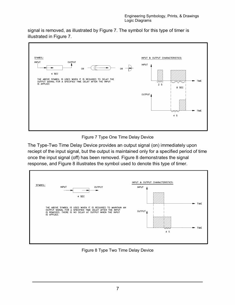
Upon receipt of the input signal, the Type-One Time Delay Device delays the output
(on) for the specified period of time, but the output will stop (off) as soon as the input
Engineering Symbology, Prints, & Drawings Logic Diagrams
7
signal is removed, as illustrated by Figure 7. The symbol for this type of timer is
illustrated in Figure 7.
Figure 7 Type One Time Delay Device
The Type-Two Time Delay Device provides an output signal (on) immediately upon
reciept of the input signal, but the output is maintained only for a specified period of time
once the input signal (off) has been removed. Figure 8 demonstrates the signal
response, and Figure 8 illustrates the symbol used to denote this type of timer.
Figure 8 Type Two Time Delay Device

Engineering Symbology, Prints, & Drawings Logic Diagrams
8
Upon reciept of an input signal, Type-Three Time Delay Devices provide an output
signal for a specified period of time, regardless of the duration of the input. Figure 9
demonstrates the signal response and illustrates the symbol used to denote the timer.
Figure 9 Type-Three Time Delay Device
Complex Logic Devices
In addition to the seven basic logic gates, there are several complex logic devices that
may be encountered in the use of logic prints.
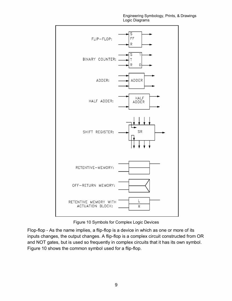
Memory devices - In many circuits, a device that can "remember" the last command or
the last position is required for a circuit to function. Like the AND and OR gates,
memory devices have been designed to work with on/off signals. The two input signals
to a memory device are called set and reset. Figure 10 shows the common symbols
used for memory devices.
Engineering Symbology, Prints, & Drawings Logic Diagrams
9
Figure 10 Symbols for Complex Logic Devices
Flop-flop - As the name implies, a flip-flop is a device in which as one or more of its
inputs changes, the output changes. A flip-flop is a complex circuit constructed from OR
and NOT gates, but is used so frequently in complex circuits that it has its own symbol.
Figure 10 shows the common symbol used for a flip-flop.

Engineering Symbology, Prints, & Drawings Logic Diagrams
10
This device, although occasionally used on component and system type logic diagrams,
is principally used in solid state logic diagrams (computers).
Binary counter - Several types of binary counters exist, all of which are constructed of
flip-flops. The purpose of a counter is to allow a computer to count higher than 1, which
is the highest number a single flip-flop can represent. By ganging flip-flops, higher
binary numbers can be constructed. Figure 10 illustrates a common symbol used for a
binary counter.
Shift register - Is a storage device constructed of flip-flops that is used in computers to
provide temporary storage of a binary word. Figure 10 shows the common symbol used
for a shift register.
Half adder - Is a logic circuit that is used in computer circuits to allow the computer to
"carry" numbers when it is performing mathematical operations (for example to perform
the addition of 9 + 2, a single 1 0s unit must be "carried" from the ones column to the
tens column). Figure 10 illustrates the symbol used for a half adder.
Summary
The important information in this chapter is summarized below.
Engineering Logic Diagrams Summary
This chapter reviewed the seven basic symbols used on logic diagrams and
the symbols used for six of the more complex logic devices.
There are three types of time delay devices:
o Type One - delays the output signal for a specified period of time
o Type Two - only generates an output for the specified period of time
o Type Three - receipt of an input signal triggers the device to output a
signal for the specified time, regardless of the duration of the input

Engineering Symbology, Prints, & Drawings Truth Tables & Exercises
11
TRUTH TABLES AND EXERCISES
Truth tables offer a simple and easy to understand tool that can be used to
determine the output of any logic gate or circuit for all input combinations.
EO 1.3 DEVELOP the truth tables for the following logic gates:
a. AND gate d. NAND gate
b. OR gate e. NOR gate
c. NOT gate f. EXCLUSIVE OR gate
EO 1.4 IDENTIFY the symbols used to denote a logical 1 (or high) and a
logical 0 (or low) as used in logic diagrams.
EO 1.5 Given a logic diagram and appropriate information, DETERMINE the
output of each component and the logic circuit.
Truth Tables
When a logic gate has only two inputs, or the logic circuit to be analyzed has only one
or two gates, it is fairly easy to remember how a specific gate responds and determine
the output of the gate or circuit. But as the number of inputs and/or the complexity of the
circuit grows, it becomes more difficult to determine the output of the gate or circuit.
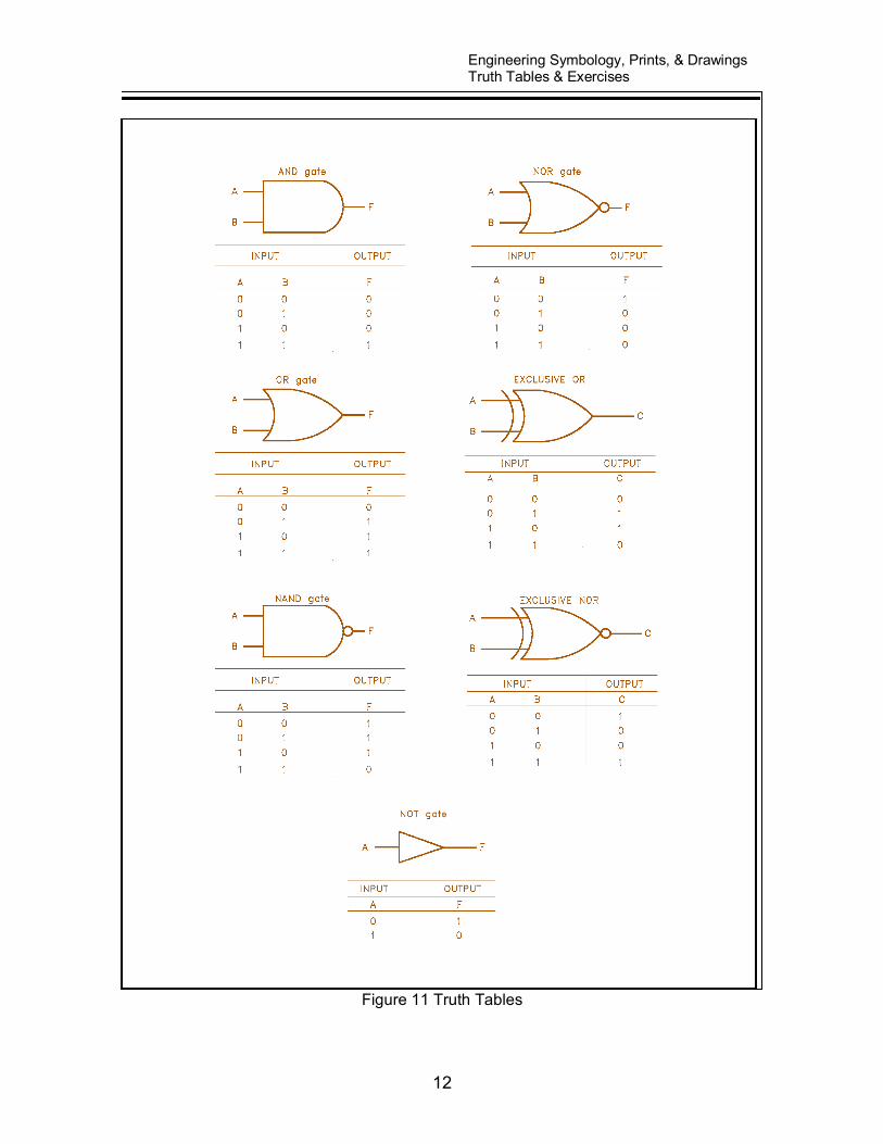
Truth tables, as illustrated in Figure 11, are tools designed to help solve this problem. A
truth table has a column for the input of each gate and column for the output of each
gate. The number of rows needed is based on the number of inputs, so that every
combination of input signal is listed (mathematically the number of rows is 2n, where n =
number of inputs). In truth tables, the on and off status of the inputs and outputs is
represented using 0s and 1s. As previously stated 0 = off and 1 = on. Figure 11 lists
truth tables for the seven basic logic gates. Compare each gate's truth table with its
definition given earlier in this module, and verify for yourself that they are stating the
same thing.
Engineering Symbology, Prints, & Drawings Truth Tables & Exercises
12
Figure 11 Truth Tables
Engineering Symbology, Prints, & Drawings Truth Tables & Exercises
13
Reading Logic Diagrams
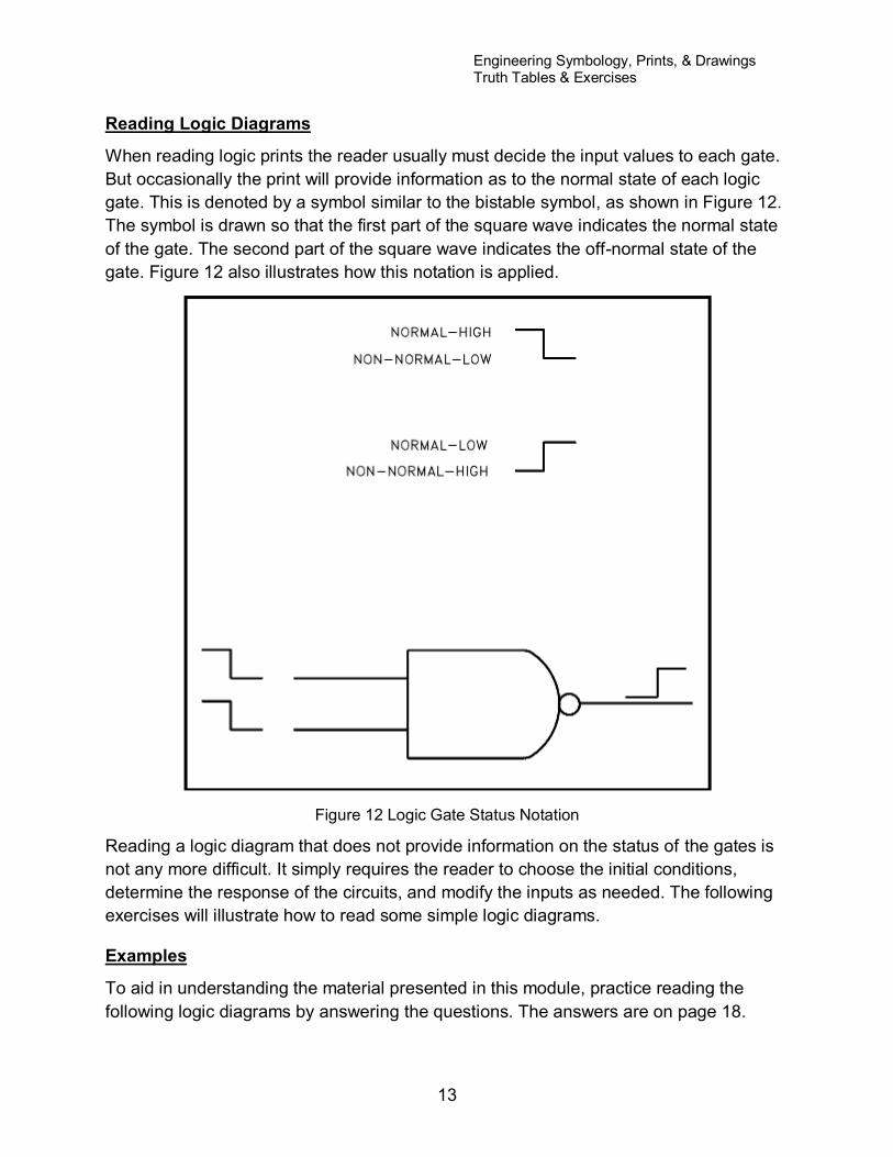
When reading logic prints the reader usually must decide the input values to each gate.
But occasionally the print will provide information as to the normal state of each logic
gate. This is denoted by a symbol similar to the bistable symbol, as shown in Figure 12.
The symbol is drawn so that the first part of the square wave indicates the normal state
of the gate. The second part of the square wave indicates the off-normal state of the
gate. Figure 12 also illustrates how this notation is applied.
Figure 12 Logic Gate Status Notation
Reading a logic diagram that does not provide information on the status of the gates is
not any more difficult. It simply requires the reader to choose the initial conditions,
determine the response of the circuits, and modify the inputs as needed. The following
exercises will illustrate how to read some simple logic diagrams.
Examples
To aid in understanding the material presented in this module, practice reading the
following logic diagrams by answering the questions. The answers are on page 18.
Engineering Symbology, Prints, & Drawings Truth Tables & Exercises
14
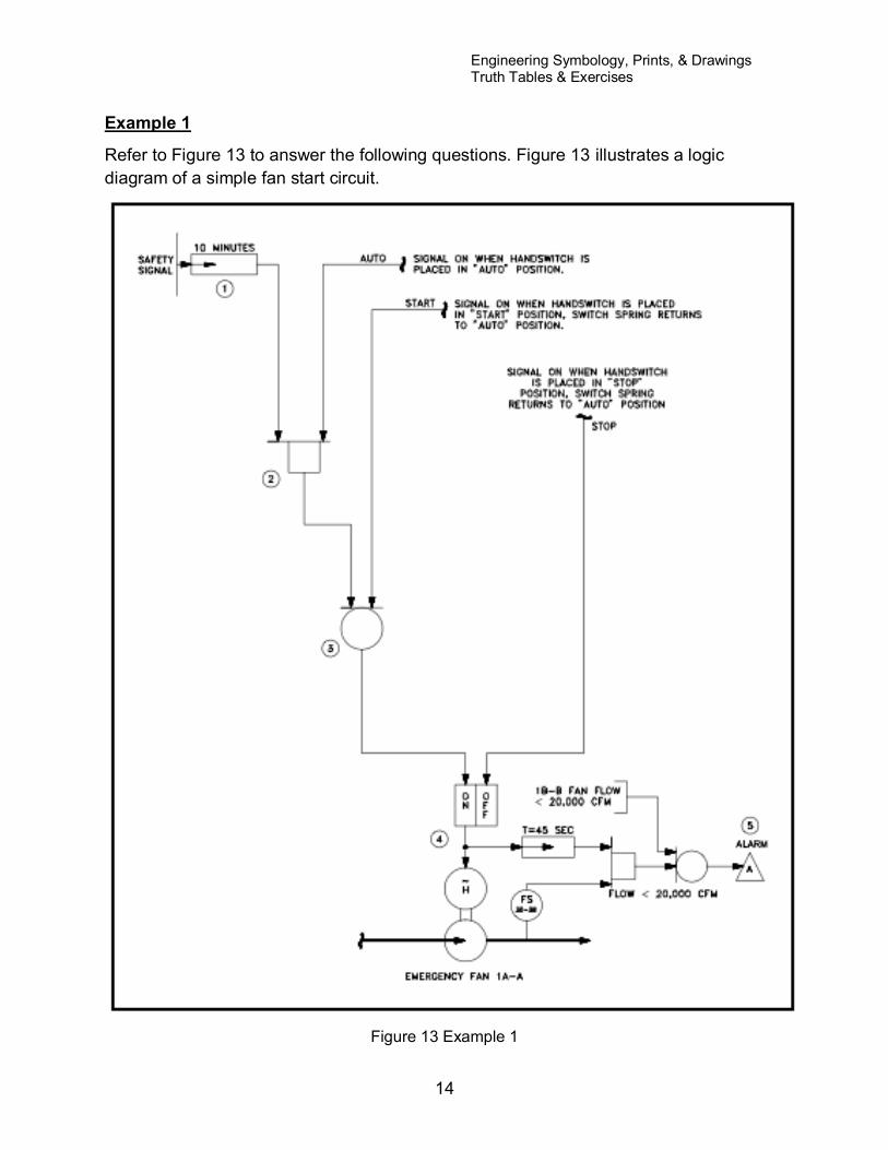
Example 1
Refer to Figure 13 to answer the following questions. Figure 13 illustrates a logic
diagram of a simple fan start circuit.
Figure 13 Example 1
Engineering Symbology, Prints, & Drawings Truth Tables & Exercises
15
1. Identify by number the following logic symbols:
_____ a. AND
_____ b. OR
_____ c. Time delay
_____ d. Retentive-Memory
2. How long must the safety signal be present before the time delay (1) will pass an
output (on) signal to Gate 2?
3. Under what conditions will Gate 2 turn on?
4. Under what conditions will the low flow alarm (5) sound?
5. Since the control switch is always in the AUTO position (due to the spring return
feature), what logic gate keeps the continuous on signal that is generated by the
control switch being in the AUTO position from starting the fan? What signal must
also be present to allow the AUTO signal to start the fan?
6. If 12 minutes after first receiving a safety signal, with the fan control switch in the
AUTO position, the safety signal is removed (off), what will happen to the fan?
Why?
7. How many ways can the fan be started? How many ways can the fan be
stopped?
Engineering Symbology, Prints, & Drawings Truth Tables & Exercises
16
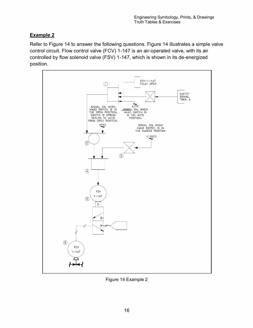
Example 2
Refer to Figure 14 to answer the following questions. Figure 14 illustrates a simple valve
control circuit. Flow control valve (FCV) 1-147 is an air-operated valve, with its air
controlled by flow solenoid valve (FSV) 1-147, which is shown in its de-energized
position.
Figure 14 Example 2

Engineering Symbology, Prints, & Drawings Truth Tables & Exercises
17
1. Identify by number the following logic symbols.
_____ a. AND
_____ b. OR
_____ c. NOT
2. As drawn, with the hand switch in the AUTO position and no safety signal
present, what is the status of the two inputs to Gate 4, on or off?
3. Since electrical components are drawn in their de-energized state, and using the
answer from Question 2, is the flow solenoid valve (FSV-1-147) in its correct
position? Why?
4. How many ways can FSV-1-147 be energized? De-energized?
5. If a safety signal is present, can FCV-1-147 (valve FSV-1-147 energized) be
opened? Why?
Engineering Symbology, Prints, & Drawings Truth Tables & Exercises
18
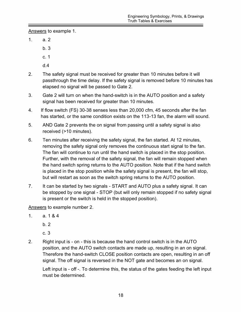
Answers to example 1.
1. a. 2
b. 3
c. 1
d.4
2. The safety signal must be received for greater than 10 minutes before it will
passthrough the time delay. If the safety signal is removed before 10 minutes has
elapsed no signal will be passed to Gate 2.
3. Gate 2 will turn on when the hand-switch is in the AUTO position and a safety
signal has been received for greater than 10 minutes.
4. If flow switch (FS) 30-38 senses less than 20,000 cfm, 45 seconds after the fan
has started, or the same condition exists on the 113-13 fan, the alarm will sound.
5. AND Gate 2 prevents the on signal from passing until a safety signal is also
received (>10 minutes).
6. Ten minutes after receiving the safety signal, the fan started. At 12 minutes,
removing the safety signal only removes the continuous start signal to the fan.
The fan will continue to run until the hand switch is placed in the stop position.
Further, with the removal of the safety signal, the fan will remain stopped when
the hand switch spring returns to the AUTO position. Note that if the hand switch
is placed in the stop position while the safety signal is present, the fan will stop,
but will restart as soon as the switch spring returns to the AUTO position.
7. It can be started by two signals - START and AUTO plus a safety signal. It can
be stopped by one signal - STOP (but will only remain stopped if no safety signal
is present or the switch is held in the stopped position).
Answers to example number 2.
1. a. 1 & 4
b. 2
c. 3
2. Right input is - on - this is because the hand control switch is in the AUTO
position, and the AUTO switch contacts are made up, resulting in an on signal.
Therefore the hand-switch CLOSE position contacts are open, resulting in an off
signal. The off signal is reversed in the NOT gate and becomes an on signal.
Left input is - off -. To determine this, the status of the gates feeding the left input
must be determined.

Engineering Symbology, Prints, & Drawings Truth Tables & Exercises
19
Looking at the OR gate (2) above it
The right input to the OR gate is - off - because the hand control
switch is in the AUTO position. The OPEN position contacts are not
made up, resulting in an off signal.
The left input to the OR gate comes from the AND gate (1) above it.
Looking at the three inputs to the AND gate. The bottom
input is - on - because the hand control switch is in the
AUTO position and the AUTO contacts are made up,
resulting in an on signal.
The middle input to the AND gate is - on - because the NOT
gate reverses the off safety signal.
The top input is - off - because the valve is not fully open,
resulting in the generation of an off signal. Note this is the
signal that, once the valve has traveled to the fully open
position, allows the valve to remain open after the hand
switch is allowed to spring return to the AUTO position.
Now that all the inputs are known, we can work back through the circuit to
determine the status of the left input to the AND gate (4).
Because the one input, the top, to the AND gate (1) is off, the output of the
AND gate is off. Therefore, the left input into the OR gate (2) is off.
Therefore, because both the left and right inputs to the OR gate (2) are off
the output of the OR gate (1) is off.
3. Yes, de-energized is correct because the left input of the AND gate (4) is off and
its right input is on. But because it is an AND gate and both its inputs are not on,
it will not pass an on signal to the solenoid to energize it.
4. It can be energized one way - the hand switch can be momentarily placed in the
OPEN position.
It can be de-energized two ways - the hand switch can be placed in the CLOSE
position, or, if the valve is open and a safety signal is received, the valve will
automatically close.
5. Yes, the valve can be opened, but it will not remain open when the hand switch is
allowed to spring return to the AUTO position. This is because the safety signal's
NOT gate removes the on signal that allows the AND gate (1) to output an on
signal and energize the solenoid.
Engineering Symbology, Prints, & Drawings Truth Tables & Exercises
20
Summary
The important information in this chapter is summarized below.
Truth Tables and Exercises Summary
The normal and off-normal status of each logic gate can be symbolized by the
use of a symbol similar to the bistable.
o The first part of the square wave indicates the normal state of the gate.
o The second part of the square wave indicates the off-normal state of the gate.
This chapter presented the truth tables for each of the seven basic logic gates.
This chapter reviewed several examples of how to read logic diagrams of simple
pump and valve circuits.