module 3: ideas to implementation - weebly
TRANSCRIPT

HSC Physics Summary | Guy Leckenby
Page | 1
Module 3: Ideas to Implementation
1. Increased understandings of cathode rays led to the development of television.
Students learn to:
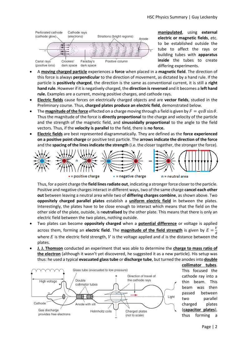
Many scientist, of which the above are just a few, investigated cathode rays. However the cathode rays produced by the discharge tubes were a mystery because they appeared to show properties of both waves and particles. The main features are shown below. This originally led to the conclusion that cathode rays were electromagnetic waves; drawn due to inadequacies in experimental procedure, like Hertz’s, and the atomic model. However as technology developed and more experiments were done, they were eventually confirmed to be particles, albeit with wave like characteristics.
With the development of the vacuum pump and the induction coil, the construction of cathode ray discharge tubes occurred. Cathode rays are streams of electrons or charged particles ejected from the cathode towards the anode under high voltage (kV) in highly evacuated glass tubes. They interact with air in different ways depending on pressure, as below, requiring low pressures to be generated at all. Discharge tubes allow these streams of charged particles to be
Scientist/ Year Relevant Observation Conclusion/ Impact
1858 – Plucker Magnets affected the discharge path. They are electrically charged. 1875 – Crookes Maltese cross, paddle tube, bent tube, etc.
experiments. Travel in straight lines, aren’t penetrating, have momentum.
1883 – Hertz Showed that cathode rays were not deflected by charged plates.
This suggests that they were waves.
1885 – Perrin Cathode rays increase the divergence of negatively charged leaves on electroscope.
They are negatively charged.
1886 – Goldstein Identified ‘canal rays’. Disproved Hertz, showing rays deflected toward positive plate.
Supports negatively charged particles.
1890 – Schuster Calculated the charge to mass ratio of cathode rays.
Too small to be ions, the smallest thing known then.
1892 – Hertz Could penetrate thin metal foil. Wave property. 1892 – Lenard Predicted their velocity to be c. EM wave property. 1894 – Thomson Proved cathode rays travel 2000 times slower
than c. Puts in doubt wave theory.
1895 – Perrin Cathode rays left a negative charge on impact.
Supports charge/ particle theory.
1897 – Thomson Measured the mass of cathode ray particles as 1800 times less than H+.
Suggested they were electrons.
Properties of particles Properties of waves
They have momentum and hence mass.
Predicted velocity was the speed of light.
Measured velocity is 2000 times slower than the speed of light.
Predicted mass was too small for any particle known.
Left a negative charge after impact on an object.
Exposed photographic plates and caused fluorescent glow.
Rays left the cathode at right angles.
They travel in straight lines and could penetrate thin foil.
HSC Physics Summary | Guy Leckenby
Page | 2
manipulated, using external electric or magnetic fields, etc. to be established outside the tube to affect the rays or building tubes with apparatus inside the tubes to create differing experiments.
A moving charged particle experiences a force when placed in a magnetic field. The direction of this force is always perpendicular to the direction of movement, as dictated by a hand rule. If the particle is positively charged, the direction is the same as conventional current, it is still a right hand rule. However if it is negatively charged, the direction is reversed and it becomes a left hand rule. Examples are a current, moving positive charges, and cathode rays.
Electric fields cause forces on electrically charged objects and are vector fields, studied in the Preliminary course. Thus, charged plates produce an electric field, demonstrated below.
The magnitude of the force effected on a charge moving through a field is given by 𝐹 = 𝑞𝑣𝐵 sin 𝜃. Thus the magnitude of the force is directly proportional to the charge and velocity of the particle and the strength of the magnetic field, and sinusoidally proportional to the angle to the field vectors. Thus, if the velocity is parallel to the field, there is no force.
Electric fields are best represented diagrammatically. They are defined as the force experienced on a positive point charge or positive test particle. The arrows indicate the direction of the force and the spacing of the lines indicate the strength (i.e. the closer together, the stronger the force).
Thus, for a point charge the field lines radiate out, indicating a stronger force closer to the particle. Positive and negative charges interact in different ways, two of the same charge cancel each other out between leaving a neutral area while two of differing charges combine, as shown above. Two oppositely charged parallel plates establish a uniform electric field in between the plates. Interestingly, the plates have to be close enough to interact which means that the field on the other side of the plate, outside, is neutralised by the other plate. This means that there is only an electric field between the two plates, nothing outside.
Two plates can become oppositely charged when a potential difference or voltage is applied
across them, forming an electric field. The magnitude of the field strength is given by 𝐸 =𝑉
𝑑
where 𝐸 is the electric field strength, 𝑉 is the voltage applied and 𝑑 is the distance between the plates.
J. J. Thomson conducted an experiment that was able to determine the charge to mass ratio of the electron (although it wasn’t yet discovered, he suggested it as a new particle). His setup was thus: he used a typical evacuated glass tube or discharge tube, but turned the anodes into double
collimator tubes. This focused the cathode ray into a thin beam. This beam was then passed between two parallel charged plates (capacitor plates), thus forming a

HSC Physics Summary | Guy Leckenby
Page | 3
uniform electric field, and simultaneously through a uniform magnetic field, generated by two current carrying coils. This established a magnetic and an electric field that were perpendicular to each other, thus both producing a force which cancelled the other out, as shown right. The deflected electrons hence continued and impacted on a fluorescent screen at the end of the bulb, emitting light. By adjusting the strengths of the magnetic and electric fields, the beam can pass undeflected. By then equating the magnetic and electric force equations (𝐸𝑞 = 𝑞𝑣𝐵) the velocity of the cathode rays can be determined. He then removed the electric field entirely leaving the same strength magnetic field and measured the radius of the circle of deflection. By the equating the magnetic force and the centripetal force
(𝑞𝑣𝐵 =𝑚𝑣2
𝑟), Thomson could calculate the charge to mass ratio of the electron (
𝑞
𝑚=
𝑣
𝐵𝑟).
For a Television or Cathode Ray Oscilloscope (CRO) to utilise cathode rays, it uses three main parts:
o In the electron gun, a heating filament heats the cathode to help release electrons via thermionic emission. The electrodes have an extremely high voltage passed through, as required by cathode rays, which accelerates them to the high speed required to excite the phosphor. The density of electrons determines the brightness of the image.
o Once the electron beam is focused and through the anode, there are two sets of parallel deflecting plates, electrically charged such that an electric field can send then beam to any coordinates on the screen. These direct the beam to the appropriate place on the screen.
o When the electron beam reaches the fluorescent screen, the high energy electrons interact with the fluorescent material and emit light. This allows the position of the ray to be seen.
A Television has three different electron guns, each aimed for a different primary colour of light, red, green and blue. When the beam hits the fluorescent screen, each beam hits an individual fluorescent that produces that colour, thus the beam transforms into a beam of light of said colour. The shadow mask is used to focus the light beams together on the screen making a pixel. In a standard CRT TV, the picture is refreshed at around 60 Hz. A CRO enables individuals to plot any wave function or pulse, most commonly used on electrical currents and sound waves. The Y deflection plates control the displayed amplitude of the wave, or the voltage. The X deflection plates control the sweep or time base, which enables voltage to be plotted as a function of time.
HSC Physics Summary | Guy Leckenby
Page | 4
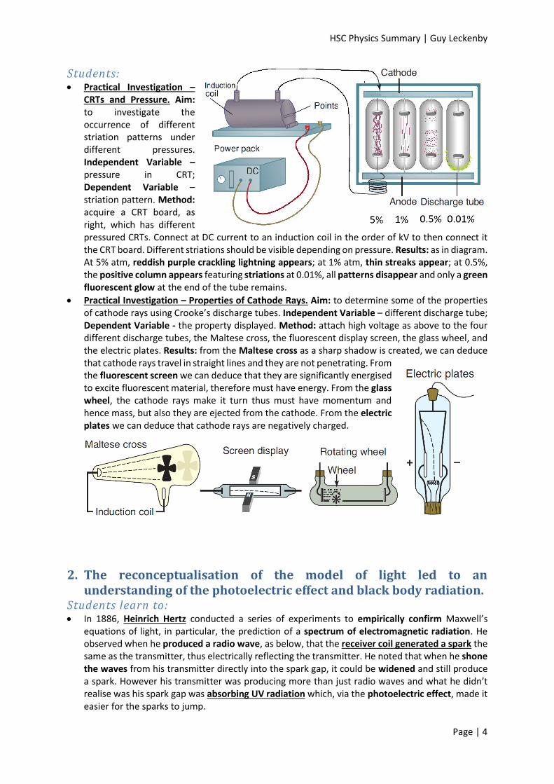
Students: Practical Investigation –
CRTs and Pressure. Aim: to investigate the occurrence of different striation patterns under different pressures. Independent Variable – pressure in CRT; Dependent Variable – striation pattern. Method: acquire a CRT board, as right, which has different pressured CRTs. Connect at DC current to an induction coil in the order of kV to then connect it the CRT board. Different striations should be visible depending on pressure. Results: as in diagram. At 5% atm, reddish purple crackling lightning appears; at 1% atm, thin streaks appear; at 0.5%, the positive column appears featuring striations at 0.01%, all patterns disappear and only a green fluorescent glow at the end of the tube remains.
Practical Investigation – Properties of Cathode Rays. Aim: to determine some of the properties of cathode rays using Crooke’s discharge tubes. Independent Variable – different discharge tube; Dependent Variable - the property displayed. Method: attach high voltage as above to the four different discharge tubes, the Maltese cross, the fluorescent display screen, the glass wheel, and the electric plates. Results: from the Maltese cross as a sharp shadow is created, we can deduce that cathode rays travel in straight lines and they are not penetrating. From the fluorescent screen we can deduce that they are significantly energised to excite fluorescent material, therefore must have energy. From the glass wheel, the cathode rays make it turn thus must have momentum and hence mass, but also they are ejected from the cathode. From the electric plates we can deduce that cathode rays are negatively charged.
2. The reconceptualisation of the model of light led to an understanding of the photoelectric effect and black body radiation.
Students learn to: In 1886, Heinrich Hertz conducted a series of experiments to empirically confirm Maxwell’s
equations of light, in particular, the prediction of a spectrum of electromagnetic radiation. He observed when he produced a radio wave, as below, that the receiver coil generated a spark the same as the transmitter, thus electrically reflecting the transmitter. He noted that when he shone the waves from his transmitter directly into the spark gap, it could be widened and still produce a spark. However his transmitter was producing more than just radio waves and what he didn’t realise was his spark gap was absorbing UV radiation which, via the photoelectric effect, made it easier for the sparks to jump.

HSC Physics Summary | Guy Leckenby
Page | 5
Hertz constructed a transmitter and connected to an induction coil which enabled quick sparks to be transmitted, as pictured right. He then established a receiving coil which could be established up to several hundred metres away. This coil also produced a spark when the transmitter sparked, despite it being electrically independent. Moreover, the spark appeared at the same time in both devices. This was the first production of radio waves, later identified. In further experiments, he proved that the rays produced interfered with each other, reflected, refracted and could even be polarised; all characteristics of light. He was able to calculate their velocity using interference patterns. He used Lloyd’s mirrors, setting up two beams; one that travelled directly to the source and one that was reflected after being emitted at a small angle. From the interference pattern produced, Hertz could calculate the wavelength and when combined with a known frequency using an oscillating circuit, the velocity could be calculated from the wave equation. Ultimately it was determined to be 𝑐, the speed of light. Undoubtedly, Hertz had proven there was an electromagnetic spectrum.
A black body is an object that will absorb all radiation falling on it. According to thermodynamics, as the temperature increases in the black body, whether from external radiation or heating, then it will reradiate radiation across the entire spectrum, each wavelength varying in intensity. Scientists constructed black bodies by creating an induction furnace with a small hole in it. As radiation was emitted as the furnace heated, it was forced to reabsorb the radiation, thus establishing an equilibrium. The radiation then exiting the hole was black body for a certain temperature, as right. Classical wave theory predicted an infinite reaction which contradicted the conservation of energy. Max Planck proposed that instead of energy being exchanged between the black body and the radiation emitted in one continuous equilibrium radiation field, it was instead exchanged as discrete quanta of energy. I.e. the interaction is particle on particle, not wave on particle. He described the energy of this quanta as 𝐸 = ℎ𝑓, where ℎ = 6.626 × 10⁻³⁴ is Planck’s constant. Planck did not believe his model accurately described reality, rather that it was merely a mathematical trick. However his quantisation of energy was the beginning of quantum theory.
Albert Einstein capitalised on Planck’s theories and suggested a particle nature of light in his 1905 paper (for which he won the Nobel Prize), using the Photoelectric effect as one example. He said that the quanta of energy that Planck described was called a photon, the smallest indivisible amount of radiation possible, described below. However technology wasn’t good enough to prove his predictions (again) and it wasn’t until 1916 that Robert Milikan begrudgingly provided the evidence, although he didn’t believe Einstein.
The particle model of light dictates that it travels through space as a procession of discrete energy bundles called photons. A photon is the smallest indivisible amount of radiation possible. As a particle in interactions, a photon could donate all of its energy or none, nothing in between. Its energy is discrete and is directly proportional to its frequency, as below. It also has a rest mass of zero and always travels at 𝑐.
The above relationship expressed mathematically is 𝐸 = ℎ𝑓, where ℎ = 6.626 × 10⁻³⁴. As all light travels at 𝑐, the wave equation can also be used, 𝑐 = 𝑓𝜆. Go and solve problems my precious!

HSC Physics Summary | Guy Leckenby
Page | 6
The Photoelectric Effect: The photoelectric effect is essentially the emission of electrons by shining a beam of light on a metal. Phillip Lenard, an assistant of Hertz, first conducted experimental investigations into the photoelectric effect in 1990. He found that light of a particular frequency exposed to an electrode in an evacuated tube caused electrons to be ejected, as right. His other observations follow (represented graphically below):
As the intensity is increased, the current flowing increases.
With increased intensity, the energy of the electrons does not increase.
When an external voltage is applied, creating an electric field, if increased the photoelectric current increases to a saturation current. If reversed (opposing) the current decreases until a stopping voltage (𝑉0) is reached. This value varies for different metals and frequencies.
If the frequency drops below a threshold frequency (ʄ0), then no current is produced, regardless of intensity. This varies for different metals.
This was explained using photons:
Individual photons have a specific energy, 𝐸 = ℎ𝑓, which is used to successfully ionise the atom in a particle collision, ejecting an electron.
As each metal’s ionisation energy varies, the energy required to ionise is known as the work function (𝑊).
Any excess energy is used as kinetic energy.
Intense light was merely more photons with the same energy, thus only increased the number of electrons ejected as each interaction was one on one.
If the photon energy was below the threshold frequency, then the individual photons didn’t have enough energy to ionise and no current was produced. The electrons were obviously ejected at all sorts of angles and energies from the lattice, so the
ones that determine the stopping voltage are the electrons ejected most perfectly, at right angles and with the greatest kinetic energy. This maximum kinetic energy can be described as 𝐸𝐾𝑚𝑎𝑥 = ℎ𝑓 − 𝑊 where 𝑊 is the work function of the metal. At the stopping voltage, a special 𝐸𝐾𝑚𝑎𝑥 is derived, where 𝐸𝐾𝑚𝑎𝑥 =𝑞𝑉0. Therefore 𝐸𝐾𝑚𝑎𝑥 is equal to the stopping voltage in electron volts. This only works at stopping voltage and describes energy of electrons that just don’t quite get there. This maximum kinetic energy of photons is graphically represented right, with each line having a gradient of ℎ as in the form 𝑦 = 𝑚𝑥 + 𝑏.
Students: Practical Investigation – Radio Waves. Aim: to demonstrate the production and reception of radio
waves. Independent Variable – the distance from induction coil; Dependent Variable – whether the radio waves are received. Method: set up an induction coil such that the gap is approximately 5 mm (such induction sparks cause X-rays that are harmful, stand clear!) and insert a switch. Using a transistor radio not tuned to a station, find the maximum distance the radio waves can be heard (using switch to confirm with interrupted signals). Increase the spark distance and repeat. Results: the waves produced with each spark will be greater with greater distance as more energy will be released with a bigger spark. Hence the further the gap, the further away sound will be heard.
HSC Physics Summary | Guy Leckenby
Page | 7
Planck in 1900 invented the fundamentals of quantum theory when describing black body radiation, that the radiation from oscillating atoms (light) must be quantised. This is an example of theory catching up to experiment, the evidence for black body radiation curves were there, just they contradicted classical models. Hence Planck’s work was crucial as it developed a new theory to explain the evidence. Einstein then developed and expanded this theory and assumed that since oscillating atoms producing light do so in a quantised form, and as all light must have a source, that all light travels in quantised form. He made detailed reference to the photoelectric effect, which was qualitatively described by Philip Lenard in 1900, as a way of experimentally validating his theory. The technology wasn’t available to test his theories however in 1916, Robert Milikan quantitatively proved his theory correct. Thus Einstein expanded on the black body radiation theory and applied it to other areas with testable predictions, proving the correlation between theory and experiment and winning a Nobel Prize whilst at it. Not bad…
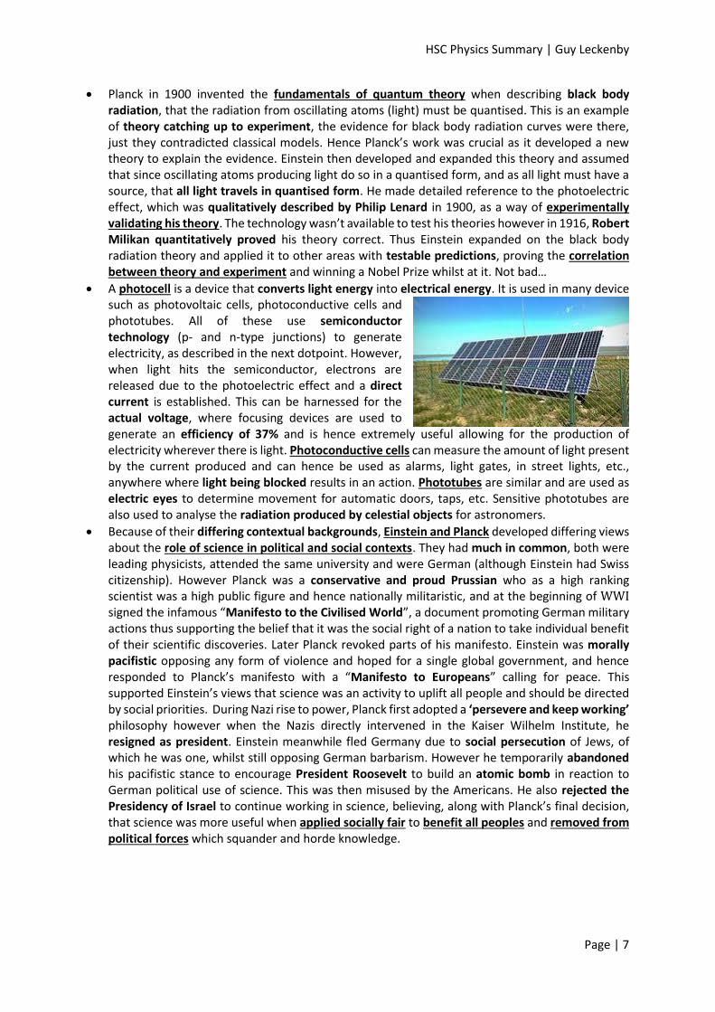
A photocell is a device that converts light energy into electrical energy. It is used in many device such as photovoltaic cells, photoconductive cells and phototubes. All of these use semiconductor technology (p- and n-type junctions) to generate electricity, as described in the next dotpoint. However, when light hits the semiconductor, electrons are released due to the photoelectric effect and a direct current is established. This can be harnessed for the actual voltage, where focusing devices are used to generate an efficiency of 37% and is hence extremely useful allowing for the production of electricity wherever there is light. Photoconductive cells can measure the amount of light present by the current produced and can hence be used as alarms, light gates, in street lights, etc., anywhere where light being blocked results in an action. Phototubes are similar and are used as electric eyes to determine movement for automatic doors, taps, etc. Sensitive phototubes are also used to analyse the radiation produced by celestial objects for astronomers.
Because of their differing contextual backgrounds, Einstein and Planck developed differing views about the role of science in political and social contexts. They had much in common, both were leading physicists, attended the same university and were German (although Einstein had Swiss citizenship). However Planck was a conservative and proud Prussian who as a high ranking scientist was a high public figure and hence nationally militaristic, and at the beginning of WWI signed the infamous “Manifesto to the Civilised World”, a document promoting German military actions thus supporting the belief that it was the social right of a nation to take individual benefit of their scientific discoveries. Later Planck revoked parts of his manifesto. Einstein was morally pacifistic opposing any form of violence and hoped for a single global government, and hence responded to Planck’s manifesto with a “Manifesto to Europeans” calling for peace. This supported Einstein’s views that science was an activity to uplift all people and should be directed by social priorities. During Nazi rise to power, Planck first adopted a ‘persevere and keep working’ philosophy however when the Nazis directly intervened in the Kaiser Wilhelm Institute, he resigned as president. Einstein meanwhile fled Germany due to social persecution of Jews, of which he was one, whilst still opposing German barbarism. However he temporarily abandoned his pacifistic stance to encourage President Roosevelt to build an atomic bomb in reaction to German political use of science. This was then misused by the Americans. He also rejected the Presidency of Israel to continue working in science, believing, along with Planck’s final decision, that science was more useful when applied socially fair to benefit all peoples and removed from political forces which squander and horde knowledge.

HSC Physics Summary | Guy Leckenby
Page | 8
3. Limitations of past technologies and increased research into the structure of the atom resulted in the invention of transistors.
Students learn to: In some solids, the outer electrons of atoms in the intermolecular structure are very loosely held
and free to be shared between atoms, hence forming a sea of electrons through the substance.
In any substance, when atoms are moved closer together, interactions with other electrons in near atoms cause the specific band energies of any given atom to diverge, as in the graph right. Thus, when atoms are bonded in solids, electrons occupy orbital bands rather than specific orbital shells. Depending on the individual atomic bonding, this can result in the outermost band, the valence band, to overlap with the conduction band, where electrons are delocalised completely. In insulators, like ionic or covalent substances, the atoms are strongly bonded such that the forbidden energy gap between the valence and conduction band is big, which causes a high electrical resistance as it take very large voltages to entice electrons into the conduction band. In conductors, like metallic lattices, the valence band clearly overlaps with the conduction band such that the majority of valence electrons are delocalised, thus giving it a very low electrical resistance and if the bands overlap more, than it is less electrically resistive. In semiconductors, there is a gap between bands however it is small and if the lattice is appropriately excited (usually though heat), then electrons will gain enough energy to jump up into the conduction band and become delocalised, thus giving it a medium electrical conductivity.
In a semiconductor, when an electron jumps to the conduction band it leaves a corresponding hole of positive charge behind, i.e. the disappearance of the negative electron in the neutral band leaves a positive hole. This positive charge is then neutralised by surrounding electrons who in turn leave their own hole. Thus, the positive hole can be transmitted through the
Conductor Semiconductor Insulator
Delocalised Electrons
Many, about 1 per atom.
Few, about one per billion atoms.
Zip, zero and zilch.
Resistivity vs Temperature
× 1015Ω
No conductivity
× 10−8Ω × 102Ω

HSC Physics Summary | Guy Leckenby
Page | 9
valence band and conduct electricity (flow of charge), although this flow is much slower in the electron zipping through the conduction band as it has to individually visit every atom.
Semiconductors are most often Group IV semimetals who form in tetrahedral lattices. The two most common are Silicon and Germanium. Germanium was used first because in WWII, it was the only element they had the technology to purify to the required standards. Even small impurities or crystalline faults will drastically affect electrical conductivity. Thus Germanium was easier to work with and it also allowed for higher frequency electrical manipulation than silicion. However when it was heated (>70°C) it became too electrically conductive such that the current would damage the electrical components. Germanium was also very expensive ($1800/kg), extremely rare on earth and always found in compound form. Thus it was quickly replaced by Silicon because it is the second most abundant element on the earth (by weight) and hence cheap ($2.5/kg), it retains its semiconducting properties at high temperatures (125°C), it can handle higher electric currents before overheating and destroying its semiconductor properties, its oxide can be made into very flat layers and doped, and the molecular structure results in uniform properties.
Doping a semiconductor is the deliberate addition of specific impurities to enhance its semiconducting properties. It is achieved by adding a group 3 or group 5 element in small quantities to a pure semiconductor, say silicon. This disparity in valence electrons allows for the creation of an extra energy level in the forbidden energy gap which means that electrons require less energy to be excited into the conduction band, increasing conductivity. Only a small amount of dopant is required, one dopant in every 200,000 silicon atoms. Doping is achieved through various methods, like diffusion.
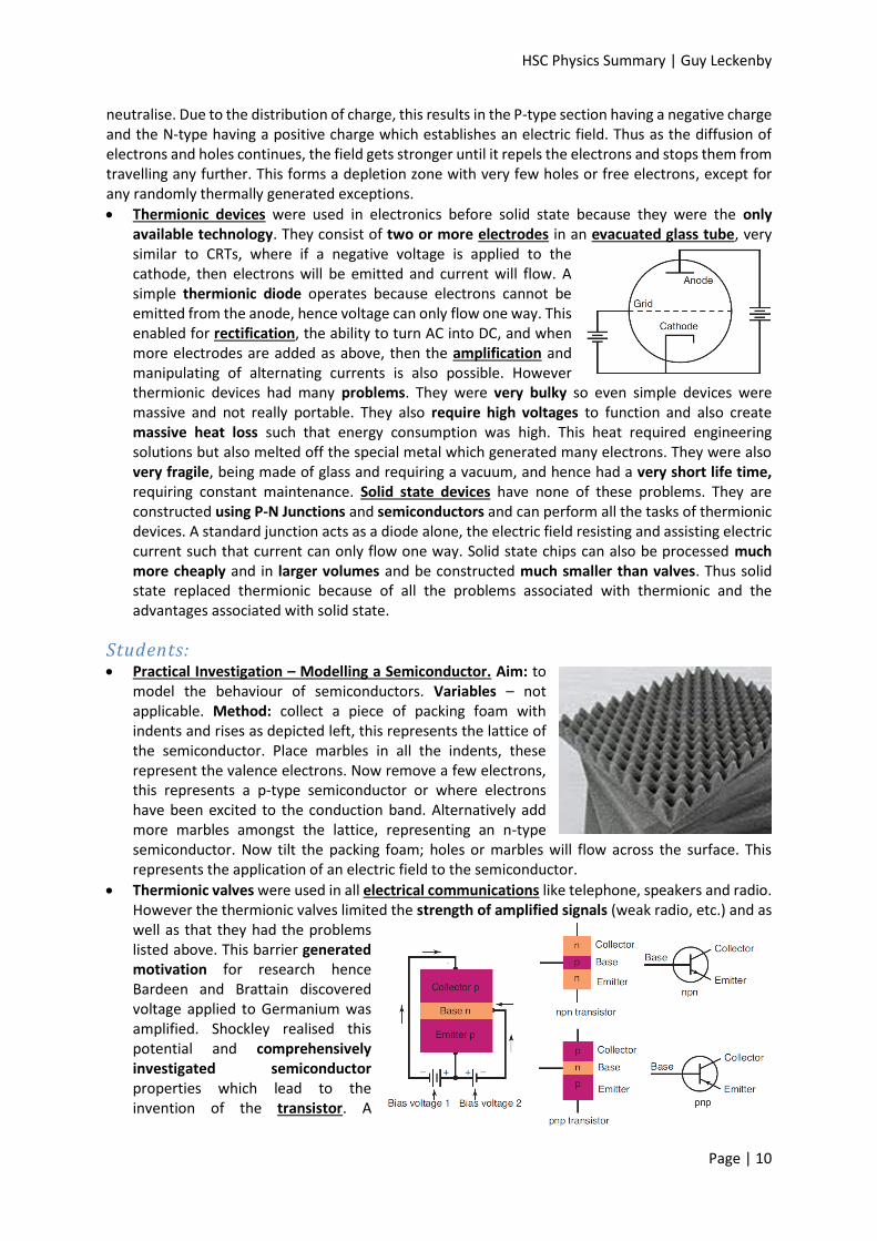
There are two types of doping, p- and n-type. P-type is the addition of a group three element, like Gallium or Boron. This atom bonds into the lattice as shown left however with one less valence electron so it leaves a hole behind, a hole of positive charge, as before. This hole creates an acceptor level in the forbidden energy gap such that electrons who fill it require less energy to then be excited to the conduction band, thus increasing its electrical conductivity. Because the ratio of holes to electrons is greater than a normal semiconductor, it mainly uses positive holes to change its electrical properties, hence positive or p-type. N-type is the addition of a group 5 such as Arsenic or Phosphorus that when bonded in the lattice, one valence electron is left over. This spare electron creates a donor level, not quite in the conduction band, but requiring very little energy to excite it, hence increasing conductivity. Because it uses spare electrons to change its properties, or negative charge carriers, it is termed negative or n-type.
The P-N Junction: is the special case when opposing doped semiconductors meet. The P-type has many acceptor atoms who will accept an electron to fill their positive hole. The N-type has donor atoms with spare electrons so the electrons from the N-type travel to the holes of the P-type and
HSC Physics Summary | Guy Leckenby
Page | 10
neutralise. Due to the distribution of charge, this results in the P-type section having a negative charge and the N-type having a positive charge which establishes an electric field. Thus as the diffusion of electrons and holes continues, the field gets stronger until it repels the electrons and stops them from travelling any further. This forms a depletion zone with very few holes or free electrons, except for any randomly thermally generated exceptions.
Thermionic devices were used in electronics before solid state because they were the only available technology. They consist of two or more electrodes in an evacuated glass tube, very similar to CRTs, where if a negative voltage is applied to the cathode, then electrons will be emitted and current will flow. A simple thermionic diode operates because electrons cannot be emitted from the anode, hence voltage can only flow one way. This enabled for rectification, the ability to turn AC into DC, and when more electrodes are added as above, then the amplification and manipulating of alternating currents is also possible. However thermionic devices had many problems. They were very bulky so even simple devices were massive and not really portable. They also require high voltages to function and also create massive heat loss such that energy consumption was high. This heat required engineering solutions but also melted off the special metal which generated many electrons. They were also very fragile, being made of glass and requiring a vacuum, and hence had a very short life time, requiring constant maintenance. Solid state devices have none of these problems. They are constructed using P-N Junctions and semiconductors and can perform all the tasks of thermionic devices. A standard junction acts as a diode alone, the electric field resisting and assisting electric current such that current can only flow one way. Solid state chips can also be processed much more cheaply and in larger volumes and be constructed much smaller than valves. Thus solid state replaced thermionic because of all the problems associated with thermionic and the advantages associated with solid state.
Students: Practical Investigation – Modelling a Semiconductor. Aim: to
model the behaviour of semiconductors. Variables – not applicable. Method: collect a piece of packing foam with indents and rises as depicted left, this represents the lattice of the semiconductor. Place marbles in all the indents, these represent the valence electrons. Now remove a few electrons, this represents a p-type semiconductor or where electrons have been excited to the conduction band. Alternatively add more marbles amongst the lattice, representing an n-type semiconductor. Now tilt the packing foam; holes or marbles will flow across the surface. This represents the application of an electric field to the semiconductor.
Thermionic valves were used in all electrical communications like telephone, speakers and radio. However the thermionic valves limited the strength of amplified signals (weak radio, etc.) and as well as that they had the problems listed above. This barrier generated motivation for research hence Bardeen and Brattain discovered voltage applied to Germanium was amplified. Shockley realised this potential and comprehensively investigated semiconductor properties which lead to the invention of the transistor. A

HSC Physics Summary | Guy Leckenby
Page | 11
transistor is a semiconductor that can act as a switch or amplifier and is the combination of two P-N junctions in close proximity. The transistor consists of three regions; the collector and emitter are the same type whilst the base is opposite thinner. Each junction must be correctly biased for the transistor to function. When the bias to the base varies, they can vary the amplification and hence the signal strength produced, allowing it to also function as a switch; greater than this voltage, ON, less OFF.
With the invention of semiconductor transistors, solid state soon replaced thermionic but only on a discrete level. Next came integrated circuits, tiny circuits made from silicon chips that can act like the larger thermionic systems however all of the interconnections are built into the chip so they are self-contained units. Some of the larger microchips today contain up to five million circuit components like transistors and resistors. These microchips are built up from silicon wafers (treated with other materials as well) three dimensionally constructed with projected light imprinting. The chips are assembled into packages containing all of the external connections to facilitate insertion into printed circuit boards. This enabled the miniaturisation of electronics and the possibility of microprocessors. This has had a massive impact on global society, all electronics uses these microchips which have enabled society to become much more efficient. They have improved standards of living, exponentially increased communication, made military more powerful, reduced manual labour, etc. Thus, transistors have led to a massive global change.
Photovoltaic Cells are applications of the photoelectric effect and the P-N junction. When the junction is established, an electric field is also established throughout the cell acting like a diode. When photons arrive and excite the electrons in the semiconductor, the holes and electrons carry charge across the junction. When the junction is connected to a metal contact grid it acts as a terminal such that the electrons can escape through a circuit and perform work on some load. If the grid is large, it reflects light but has decreased resistance. Thus, there is a trade. Once they complete the circuit, they nullify the holes awaiting for them. Thus the energy of the photons is transformed into electrical energy. To increase voltage or current multiple cells are connected in parallel or series.
4. Investigations into the electrical properties of particular metals at different temperatures led to the identification of superconductivity and the exploration of possible applications.
Students learn to: Two scientists, William Henry Bragg
and his son William Lawrence Bragg studied the phenomena of the scattering of X-rays caused by crystal lattices. The discovery of X-rays by Roentgen in 1895 was necessary for the Braggs experiment as the diffraction of waves necessary for scattering only occurs when the

HSC Physics Summary | Guy Leckenby
Page | 12
wavelength of the wave is about the same size as the gap it is passing through and as X-rays have significantly shorter wavelengths (10−10 𝑚) than anything discovered before it made the diffraction patterns possible. The Braggs aimed X-rays at crystal structures and observed the interference patterns produced on a photographic film. By analysing the interference patterns with geometry, the exact crystal structure of the substance could be determined. To produce the X-rays, they impacted high energy electrons into copper or chromium which ejected X-rays in return. They then made the X-rays parallel using a collimator lined with molybdenum. The explanation following is an extreme simplification. As the X-rays impacted the surface of the crystal, they were reflected at various depths by differing crystal layers. As they were parallel, the X-rays emerged parallel however some had travelled further, as shown above. This produced an interference pattern from which the distance between crystal layers could be determined and hence the entire crystal modelled. This technique, and the associated mathematical law known as Bragg’s Law, was used by many after to study the structure of substances and helped with the discovery of DNA, transistors and microchips. The Braggs won a Nobel Prize for this work in 1915.
When solid metals are formed, the molecules arrange themselves in an ordered geometrical pattern producing a uniform crystal lattice. This was hypothesised but Bragg Crystallography was able to confirm the theory, including the fact that in a metal lattice the individual atoms are close enough such that their valence electron shells overlap and delocalise the electrons.
In an ordinary lattice, the delocalised electrons are moving in all directions at high velocities, however there is not net charge movement as it is purely random. However when an electrical potential or field is applied, the electrons come under force and thus, although the movement is largely random, the net movement or drift velocity is directly proportional to the voltage applied otherwise known as current. The greater the cross section of the metal, the more electrons are able to move, the greater current can be applied. Thus, conduction in a lattice is the free movement of delocalised electrons largely unimpeded by the lattice.
Some collisions and interactions between ions and other electrons generate heat in the lattice, i.e. further lattice vibrations. Thus, the more a lattice vibrates, the greater chance of electron collision or electron scattering and hence energy loss. When the current is steady, all the energy lost in used in increasing lattice vibrations, i.e. resistance or joule heating. The presence of impurities or imperfections in the lattice greatly increase the chance of electron collision and thus increase resistance.
Superconductivity is the occurrence of near zero resistance at cold temperatures. When superconducting, the electrons pass perfectly unimpeded through the lattice with no collisions, thus no heat or resistance. This is possible due to the formation of electron Cooper pairs which interact with each other and the lattice to eliminate resistance.
From the discovery of superconductivity in 1911 it took 46 years to come up with a theoretical explanation that relies on quantum mechanics anyway. This is called the BCS theory (after its inventors, Bardeen, Cooper and Schrieffer) and is useful to observe the meaning of a model in science. The BCS theory relies two main concepts, phonons and Cooper pairs. A phonon is quantum of lattice vibration. Due to the extremely cold temperatures, phonons are mainly produced by interactions with electrons. From a classical point of view, electrons can pair together in Cooper pairs that are constantly breaking and reforming such that when travelling through a still lattice, the Coulomb attraction between the lattice and electrons causes the lattice to bend in

HSC Physics Summary | Guy Leckenby
Page | 13
towards the electrons generating a phonon, as right. The contraction of the lattice and mass of positive charge attracts the electron behind, pulling it forward and hence absorbing the phonon. Thus, zero resistance is achieved. However this model breaks down because to be close enough to exchange phonons, the Cooper pairs would also repel each other, amongst other issues. Instead, quantum mechanics can be considered. To reach a lower energy state, an electron can be cooled such that it jumps down an energy gap (although still independent). To jump back up again and destroy the superconducting effect requires significant energy input (equal to 𝑇𝑐) so the electrons are stable here. Once here it can form a Cooper pair with another electron of opposite spin (refer to Quanta to Quark). By exchanging phonons from distance, the electrons combine spin such that instead of acting as a
fermion (spin ±1
2) they can act as a boson (integer spin). This means they no longer obey Pauli’s
exclusion principle and hence all electrons can condense to the lowest energy state. Thus, millions of Cooper pairs could occupy the same space without overlapping and could hence assist each other to move through the lattice unimpeded. This also allowed Cooper pairs to be formed over large distance travelling in different directions. This quantum mechanical explanation solved all the problems associated with metallic (Type I) superconductors however could not explain the ceramic (Type II) superconductors whose 𝑇𝑐 was much higher (in fact there still is no explanation). This is a good example of two different models that explain the same thing to differing degrees of accuracy.
The most obvious advantage of superconductors is their lack of electrical resistance. This means no energy loss when electrical currents are passed through and can use thinner wires to no detriment which is useful for economic power storage and transmission. Through the Meissner Effect, they can generate extremely powerful magnetic fields per unit weight which is useful for motors and generators, MRI and maglev trains. However they have a maximum current (fixed for each superconductor regardless of shape) that can be applied before properties are lost, which limits some uses. They are also very expensive to keep below the critical temperature which counters their economic advantages in most cases. Type II superconductors are raising this limit to rates for cooling by liquid nitrogen (much cheaper) however these are difficult to produce, chemically unstable, brittle, and non-ductile which limits even their uses. Thus superconducting technology needs significant improvement to become economically effective in many situations.
Students: An example of magnetic levitation is the
Meissner effect. Immerse a high TC superconductor in liquid nitrogen such that it becomes superconductive and hold a rare earth magnet over the superconductor as pictured below. The magnet will interact with the superconductor to cause magnetic levitation.
The Meissner Effect is the property of all superconductors to expel magnetic fields. When a superconductor is placed in a magnetic field, the magnetic field will induce a current within the superconductor. This current induces a magnetic field that is exactly opposite in direction to the

HSC Physics Summary | Guy Leckenby
Page | 14
external magnetic field as there is no energy lost in the induction, thus cancelling the field and expelling all magnetic flux from the superconductor. These are not eddy currents as they require relative motion whereas once the current is established, it will infinitely flow with no change in flux. If the external field changes, the currents will change to match. As all flux lines must flow from a north to a south uninterrupted, the magnetic field will be forced to bend and strengthen around the superconductor as a result and thus allow for levitation, the magnetic field will become strong enough to cancel gravity.
Maglev Trains are trains suspended by magnetic levitation. This enables no contact with solid surfaces where the only frictional resistance is air resistance reaching speeds of 517 kmh-1. The electrodynamic system (EDS) used in Japan has superconducting electromagnets where the zero resistance and infinite current enable extremely strong magnetic fields to be produced. Electrically conductive strips are laid on the track which induce opposing magnetic fields to enable levitation. The propulsion system uses alternating electromagnets to produce a constant repulsion/attraction action to accelerate the train. They are currently impractical due to the enormous electrical requirements to maintain superconductivity.
The applications of superconductors are practically ultimate, including: o Computers: the current size and speed of microchips are limited by the production of heat
and conducting speed. Superconductive film would result in more densely packed transistors and reduce the processing time by several orders of magnitude. Thus there is massive potential for applications in electronics and computing.
o Motors and Generators: with the use of superconductor electromagnets, the current stator magnets could be reduced to a fraction of the size for the same power and would remove the need for iron cores to increase the efficiency. Thus, superconductors would enable motors and generators to be more powerful, smaller and more efficient.
o Electrical Transmission: if high temperature superconductors could overcome their current brittleness, then new thin wires could carry 3 to 5 times the current which would reduce line loss cost and metallic wire cost. A current problem is of peak consumption. Because electrical energy cannot be stored, power stations must produce electricity at peak consumption 24/7. Superconducting magnetic energy storage (SMES) allows for electrical energy to be stored in superconductors where the current runs infinitely without energy loss. Thus stations could produce energy at average consumption and still provide the required energy which would vastly reduce energy costs.
Superconductor Compound TC (K)
Mercury (Mg) Metal 4.2 Lead (Pb) Metal 7.2 Vanadium Silicate (V3Si) Alloy 16.9 Niobium Aluminate (Nb3Al) Alloy 18.7 Yttrium-Barium-Copper Oxide (YBa2Cu3O7)
Ceramic 92
Thallium-Barium-Calcium-Copper Oxide (Th2Ba2Ca2Cu3O10)
Ceramic 125