module -11 decoder table of contents - e-pgpathshala
TRANSCRIPT

1
Electronic Science Digital Electronics 11. Decoders
Module -11
Decoder
Table of Contents
1. Introduction
2.Basics of Decoders 2.1 Binary Decoders
2.1.1 A 2 to 4 line Decoder 2.1.2 A 3 to 8 line (Binary to Octal) Decoder 2.1.3 A 4 to 16 line (Binary to Hexadecimal) Decoder 2.1.4 BCD to Decimal Decoder
2.2 Special Decoders 2.2.1 BCD to seven segment decoder
3 Applications 3.1 Leading zero suppression 3.2 Multiplexed display 3.3 Time division multiplexing 3.4 Address decoder
3.5 Function generator
4. Summary
Learning outcome –
After studying this module, you will be able to: 1. Understand the importance of decoders
2. Learn the principles of decoding 3. Study the types of decoders and their design 4. Get familiar with the applications of decoders.

2
Electronic Science Digital Electronics 11. Decoders
1. Introduction
Decoders are digital systems which are used for decoding the information. In other words, the
decoders decrypt or retrieve the actual data from the received code. It converts the binary input
code into the desired output format. In all Modern digital system like calculators, mobile
phones, fax machines, computers and other digital gadgets, encoder is used at input side for
encoding and decoder is used at output side for decoding. There is a wide variety of applications
like data de-multiplexing, memory address decoding, seven segment display decoding, binary
function generator etc.
Fig. 1: Simple block diagram of Digital system showing encoder and decoder
Figure -1 indicates the position of encoder and decoder in the digital system. Encoders receive
the input from the keyboard to generate binary for further processing. Decoder accepts the
processed binary code and converts back in the format useful for output devices like seven
segment display, CRT, Printers etc. Let us now study the decoder in details.
2. Basics of Decoder
Decoder is a combinational logic circuit that converts abinary code into the desired output
signals. It is called decoder because it performs the reverse process of encoder. The process of
converting binaryinput code into desirable output is known as decoding.

3
Electronic Science Digital Electronics 11. Decoders
Figure 2 is the logic symbol of decoder with ‘n’ inputs and ‘m’ outputs. In short, it is multiple
inputs and multiple outputs device with proper conversion system. Note that decoder performs
the reverse operation of the encoder.
Fig. 2: Logic Symbol of a Decoder
A decoder has ‘n’ number of input lines and ‘m’ number of output lines. There are 2n possible
input combinations and the number of outputs (m) are less than or equal to 2n .Here the number
of outputs can have following relation
Decoder converts an n bit code to single active output. The information present in one code is
obtained back into the desired code. In general Decoder is circuit which convert specific code
into more general form of code.
• A decoder is a logic circuit that accepts a set of inputs that represents a binary number
and activates only the output that corresponds to the input binary number.
• In other words, a decoder circuit looks at its inputs, determines which binary number is
present and activates the one output that corresponds to that number; all other outputs
remain inactive
The basic function of a decoder is used to detect the presence of a specified combination of bits
(code) on its inputs and to indicate the presence of that code by a specific output level. In its
nm 2≤

4
Electronic Science Digital Electronics 11. Decoders
general form, a decoder has n input lines to handle n bits and from one out of 2n output lines to
indicate the presence of one or more n bit combinations.
A decoder is similar to de-multiplexer without Data input. The only inputs are the select inputs
or control inputs.As its name indicates, a decoder is a circuit that decodes an input code. Givena
binary code of n-bits, a decoder will tell which code is this out of the 2n possible codes.
Fig. 3: Classification of decoders
There are two types of decoders: linear or binary decoders and special decoders as shown in
figure 3.In binary (or linear) decoder, only one output line corresponding to input binary code is
activated. Whereas the special decoders do not limit activation of single output like binary
decoder/demultiplexer but can have more than two outputs activated at a time.
2.1 Linear or Binary decoders
A basic decoder is basically a multiple-input and multiple output logic devices that converts
coded inputs into coded output. Here input and output codes are different in type and size. The
binary decoder is n-line to 2n line decoder. These decoders convert binary information from n
coded inputs to maximum of 2n unique outputs. Typical examples are 2 to 4 line decoder, 3 to 8
decoder or 4 to 16 decoder and so on. Thus, the decoder can decode a two, three or four-bit
Decoders
Linear Decoders
2 to 4 line 3 to 8 line4 to 16 line
(BCD to Decimal)
Special Decoders
7-segment Decoder

5
Electronic Science Digital Electronics 11. Decoders
binary number. Decoder may have less than 2n outputs e.g. BCD to decimal decoder. Table-1
indicates a list of decoder ICs available in TTL logic family.
Table-1: TTL ICs for Decoder
IC Number Description Output
74138 3 to 8 line decoder/demultiplexer Inverted output
74139 2 to 4 line decoder/demultiplexerr Inverted output
74155 2 to 4 line decoder/demultiplexer Complementary
74156 2 to 4 line decoder/demultiplexer Open collector
74154 4 to 16 line decoder/demultiplexer Same as input
74159 4 to 16 line decoder/demultiplexer Open collector
2.1.1 A 2 to 4 line decoder
The simplest decoder is a 2 to 4 line decoder. It has two inputs S1 and S0 and four outputs
denoted by Y0, Y1, Y2 and Y3. Figure 3 indicates the logic symbol and Truth table of 2 to 4 line
decoder. The output of the decoder is active HIGH. In this decoder, note that S1 represents MSB
and S0 is the LSB of the input code.
Figure-4: Logic Symbol and Truth Table of 2 to 4 line decoder
Inputs Outputs
S1 S0 Y0 Y1 Y2 Y3
0 0 1 0 0 0
0 1 0 1 0 0
1 0 0 0 1 0
1 1 0 0 0 1

6
Electronic Science Digital Electronics 11. Decoders
From the truth table of 2 to 4 line decoder, one can obtain the Boolean expression for each
output. From these logic expressions, it is possible to draw the logic diagram for 2 to 4 line
decoder.
Figure 5: Logic diagram of 2 to 4 line decoder
The logic diagram of 2 to 4 line decoder is shown in fig. 5. The logic diagram is generated with
the help of AND gates and Inverters. AND gate provides the product terms or MINTERMS of
the decoder for input combination.
Active LOW decoder In many applications, decoders are designed with active low output. In such a case AND gates
are replaced by NAND gates. Other interconnections with select inputs are unchanged. Fig. 6
shows the active LOW 2 to 4 line decoder

7
Electronic Science Digital Electronics 11. Decoders
Figure 6: Active LOW 2 to 4 line decoder
Generally, decoders have the “enable” input .The enable input performs no logical
operation, but is only used for making the decoder ACTIVE or INACTIVE.
1. If the enable E is zero, then all outputs are zero regardless of the input values.
2. If E is ‘1’, then the decoder performs its normal operation. Such decoder has active HIGH enable inputs. In many decoders active LOW enable input is also
preferred.
2.1.2 A 3 to 8 (Binary to Octal) decoder
In three to eight decoder, there are three inputs and eight outputs, as shown in figure 7. S0 is the
least significant variable, while S2 is the most significant variable. The three inputs are decoded
into eight outputs namely Y0, Y1,…Y7 . The function table indicates, binary values at the input
from eight combinations activate the corresponding output line.
This 3 to 8 line decoder is also known as binary to octal decoder.

8
Electronic Science Digital Electronics 11. Decoders
Figure 7: Logic symbol and function table of 3 to 8 line decoder
Figure 8: A 3 to 8 (binary to octal) decoder

9
Electronic Science Digital Electronics 11. Decoders
In three to eight decoder, there are three inputs and eight outputs, as shown in fig. 8. A 3 to 8
line decoder generates 8 product terms corresponding to each binary code applied at the three
inputs. Thus there is a need of eight 3-input AND gates and 3 NOT gates to generate the
complement of input along with un-complemented input. It is possible to verify the truth table by
providing input condition and checking whether desired product term is activated on not.
In many decoders, there is an enable function, a LOW level on input E1,E2 and a HIGH level on
input E3, is required in order to make the enable gate output HIGH and to enable the decoding
action.
Input binary code makes only the respective output High and other outputs will be inactive i.e.
Low. When select inputs are 000 then the decoder generates only Y0=1 and other outputs are 0.
From the truth table it is clear that the input binary code decides which output is to be activated.
2.1.3 A 4 to 16 line (Binary to Hexadecimal) decoder
Figure-9: A 4 to 16 decoder
The 4 to 16 decoder is also popularly known as Binary to Hexadecimal decoder. It converts
each binary code into one of sixteen possible outputs as shown in fig. 9.

10
Electronic Science Digital Electronics 11. Decoders
The method of implementation is essentially the same as previous decoders. This decoder has 4
inputs say A, B, C and D. The 4 bit binary activates only one out of 16 possible output product
terms, which are labeled as Y0, Y1, …. Y15. All the outputs are active HIGH in this
implementation. The design implementation requires sixteen 4-input AND gates and 4 NOT
gates.
Let us now look at the scaled down version of the previous decoder. The BCD to decimal
decoder converts each binary code into one of ten possible outputs indicating decimal number.
The method of implementation is essentially the same as previous decoders. This decoder has 4
inputs say A, B, C and D. This 4 bit binary activates only one out of 16 possible product terms,
which are labeled as Y0, Y1, …. Y9. Please note that All the outputs are active LOW in this
implementation. This implementation requires Ten 4-input NAND gates and 4 NOT gates.
Active LOW outputs in the decoder are implemented using NAND gates and active HIGH
outputs are implemented using AND gates.
A list of available BCD to decimal decoder/driver ICs in TTL family is shown here. All these
decoder/driver ICs have active HIGH inputs and active LOW outputs. The outputs could be
either totem pole or pen collector form. These ICs can be used either as simple indicator or driver
for nixie tube or LED or Relay.
Table-2: TTL ICs for BCD to Decimal Decoder
IC No Description Output Applications
7441 BCD To Decimal Decoder Open Collector Output Nixie Driver
7442 BCD To Decimal Decoder Totem Pole Output LED Driver
7445 BCD To Decimal Decoder Open Collector Output Indicator/ Relay Driver
74141 BCD To Decimal Decoder Open Collector Output Nixie Tube Driver
74145 BCD To Decimal Decoder Open Collector Output Indicator/Relay Driver
74445 BCD To Decimal Decoder Open Indicator/Relay Driver

11
Electronic Science Digital Electronics 11. Decoders
2.2 Special Decoders Let us now get familiar with Special Decoders. The binary decoders studied so far generates only
one output of many in response to the binary inputs to the decoder. Whereas special decoder
activates more than one outputs simultaneously for the applied input binary code.
Many digital types of equipment require some means for displaying information. One of the
simplest and most popular methods for displaying numeric digits utilizes seven segment
configuration to for numbers 0 to 9 and sometimes the hex characters A to F.
Special decoders are designed to drive the Seven Segment display. Each segment is made up of
material that emits light when current is passed through it. Most commonly used devices include
light emitting diode (LEDs). The seven segment display has 7 LEDs for the segments and one
additional LED for dot i.e. used as decimal point.
There are two configurations for seven segment display. These are Common Anode and
Common Cathode Display.
Figure 10: Two configuration of Seven segment display
As shown in fig. 10, in common anode displays, the anodes of all LEDs are connected in
common and cathodes are labeled as a,b,c,d,e,f,g, and dp in sequential order. The common anode
requires the driving circuit to provide LOW level voltage in order to activate a given segment.
When a LOW level is applied to a segment input, the LED is forward biased and current flows
through it.

12
Electronic Science Digital Electronics 11. Decoders
2.2.1 BCD to seven segment decoder Designer can select either common anode or common cathode depending on the application. The
logic symbol of BCD to seven segment decoder / driver has 4 inputs and eight outputs is shown
in fig. 12. This BCD to seven segment decoder generates a seven segment code in response to
binary code for driving the seven segment display.
Figure 12: BCD to seven segment decoder
In order to display a decimal digit, it necessary for the decoder to activate the desired segment.
Let us now prepare a table for displaying a decimal digit and corresponding activated segments.
For displaying digit 0, LED segments a,b,c,d,e and f must be activated and segments g and dp are
OFF.
Let us now find out activated segments for displaying digit 1. Here only b and c segments must
be activated and other segments are deactivated. For displaying digit 2, LED segments a,b,g,e,d
are activated and so on.
Digit Segments Activated
0 a,b,c,d,e,f
1 b,c
2 a,b,g,e,d
3 a,b,g,c,d
4 b,c,f,g
5 a,c,d,f,g
6 a,c,d,e,f,g
7 a,b,c
8 a,b,c,d,e,f,g
9 a,b,c,f,g

13
Electronic Science Digital Electronics 11. Decoders
Let us now study the actual interfacing of BCD to seven segment decoder/driver with the seven segment display as shown in fig. 13. Here limiting resistors are connected between them. The resistor value decides the brightness of the segment.
Figure 13: Interfacing seven segment display. Let us now consider display of decimal number 2. If BCD input is 0010 then decoder generates
outputs to display decimal number 2. And so on
Table -3: BCD to seven segment decoder/driver ICs
IC No Output
Rating ( Maximum Voltage, Sink Current)
7446 Active low, open collector 30V, 40 mA
7447 Active low, open collector 15V, 40 mA
7448 Active High, Pull Up Resistor 5.5V, 6 mA
7449 Active high, open collector 5.5V, 8 mA
Let us look at the commercially available BCD to seven segment decoder / driver ICs. IC 7446
and 7447 has open collector output and the decoder requires active LOW output to drive the
common anode display configuration of 7 segment display. Whereas IC 7448 is recommended
for driving common cathode displays.

14
Electronic Science Digital Electronics 11. Decoders
Figure 14: BCD to seven segment decoder/driver ICs
In addition to 4 BCD inputs and seven segment outputs, this decoder has 3 additional pins. These
are used for special purpose.
The function of LT i.e. Lamp test terminal is to test all the seven segments of the display. As it is
active LOW input, LOW on this pin turns ON all the LED segments of the display. In normal
decoding application, this terminal should be connected to logic HIGH.
Let us now talk about BI i.e. Blanking Input. If this terminal is connected to LOW level, the
display is switched OFF irrespective of BCD inputs. This is used for conserving the power in
multiplexed display application.
RBI i.e. Ripple Blanking Input is connected to logic “HIGH” in normal decoding application. If
it is connected to LOW logic, then the segment outputs will generate the data for normal seven
segment decoding applications except BCD input Zero. Whenever all the BCD inputs are zero
corresponding to decimal zero then the seven segment display is turned OFF. This is used for
Zero blanking in multi digit display.
The RBO i.e. Ripple Blanking Output is used for cascading purpose ans is connected to RBI
terminal of succeeding stage. Normally there is a common terminal for BI and RBO in many ICs.
15
Electronic Science Digital Electronics 11. Decoders
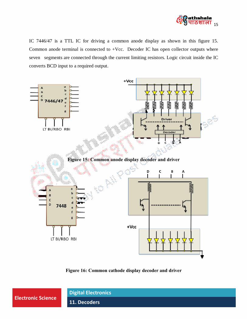
IC 7446/47 is a TTL IC for driving a common anode display as shown in this figure 15.
Common anode terminal is connected to +Vcc. Decoder IC has open collector outputs where
seven segments are connected through the current limiting resistors. Logic circuit inside the IC
converts BCD input to a required output.
Figure 15: Common anode display decoder and driver
Figure 16: Common cathode display decoder and driver

16
Electronic Science Digital Electronics 11. Decoders
IC 7448 is a TTL IC for driving a common cathode display as shown in this figure 16. Common
cathodes of all LED segments are connected to common ground.The decoder IC has its own
current limiting resistor on the chip. Logic circuit inside the IC converts BCD input to a required
output.
3. Applications There are many applications of Decoder like leading zero suppression, multiplexed display, time division multiplexing, data decoding and function generator. 1. Leading zero suppression
Figure 17: Application of decoder in Leading zero suppression
First application of decoder is in leading zero suppression. Many seven segment decoders have
built in capacity of zero suppression. This facility is useful in multi digit display. This technique
is used to blank out unnecessary zeros in the display. For example, number 35 is to be displayed
on 4 digit seven segment display. In place of displaying actually 0035 leading zeros will be
blanked out in the displayed. It may help user to read the number easily.
In this circuit, RBI of most significant display is connected to =Vcc and the RBO is connected to
RBI of the next decoder. This is the way how ripple blanking is implemented through cascading.

17
Electronic Science Digital Electronics 11. Decoders
It is also possible to implement trailing zero suppression in which zeros after the number are
suppressed, usually after decimal point.
2. Multiplexed display
Next application of the decoder is in Multiplexed display logic. In this example, single seven
segment display decoder can be used to display 2 digit data. Two BCD numbers are applied to
multiplexer inputs. When data select line is LOW, first BCD number is passed to the seven
segment decoder and generates 7-seven segment code at the output of the decoder. In addition
the IC 74139, the linear decoder enables the first display to accept data from seven segment
decoder.
Figure 18: Application of decoder in Multiplexed display logic
When data select line is HIGH, Second BCD number is passed to the seven segment decoder
and generates 7-seven segment code at the output of the decoder. In addition, the IC 74139, the
linear decoder enables the second display to accept data from seven segment decoder.
In this example, both binary and seven segment decoders are used.

18
Electronic Science Digital Electronics 11. Decoders
3. Time –division Multiplexing
Figure 19: Application of decoder in Time division mulitplexing
In this example, let us understand the use of decoder in time division multiplexing and also for
timing and sequencing. The TDM accepts data from many sources and sends a selected data to
the output for transmission. In this case output is generated in a time multiplexed manner i.e. one
at a time depending on the decoder input coming from a counter. The counter is continuously
pulsed and decoder outputs are activated sequentially A, B, C,….etc. This activates one relay at
a time to connect the data source to the output.
4. Address decoding for I/O devices
Figure 20: Application of decoder in address decoding

19
Electronic Science Digital Electronics 11. Decoders
A simplified computer I/O port system with a port address decoder with only four address lines
shown in fig. 20. Decoders are used in many types of applications. One example is in computers
for I/O selection. Computer must communicate with a variety of external devices called
peripherals by sending and/or receiving data through what is known as input/output (I/O) ports.
Each I/O port has a number, called an address, which uniquely identifies it. When the computer
wants to communicate with a particular device, it issues the appropriate address code for the I/O
port to which that particular device is connected. The binary port address is decoded and
appropriate decoder output is activated to enable the I/O port. Binary data are transferred within
the computer on a data bus, which is a set of parallel lines.
5. Function generator
Figure 21: Application of decoder in function generation
Any combinational logic circuit with n inputs and m outputs can be implemented with an n-to-
2n-line decoder and m OR gates.
Procedure:
• Express the given Boolean function in sum of min-terms
• Choose a decoder to generate all the min-terms of the input variables.

20
Electronic Science Digital Electronics 11. Decoders
• Select the inputs to each OR gate from the decoder outputs according to the list of
min-term for each function.
For adder circuit -
S(x,y,z) = Σm(1,2,4,7)
C(x,y,z) = Σm(3,5,6,7)
where Σ indicates sum, m indicates min-term and the number in brackets indicate the decimal
equivalent. Since there are three inputs and a total of eight min-terms, we need a 3-to-8 line
decoder. The decoder generates the eight min-terms for x,y,z. The OR gate for output S forms
the logical sum of min-terms 1,2, 4, and 7. The OR gates for output C forms the logical sum of
min-terms 3,5, 6, and 7
6. Other applications
There are many other applications of decoders like: Line coding and decoding for digital data
communication, Speech coding and decoding, Constructing higher order decoder and memory
addressing.
4. Summary Decoder is a combinational logic circuit that converts abinary code into the desired output signals. It is called decoder because it performs the reverse process of encoder. The process of converting binary input code into desirable output is known as decoding. A decoder has ‘n’ number of input lines and ‘m’ number of output lines. Decoder converts an n bit code to single active output. The number of outputs can have following relation
There are two types of decoders: linear or binary decoders and special decoders. The binary decoders generates only one output of many in response to the binary inputs to the decoder. Whereas special decoder activates more than one outputs simultaneously for the applied input binary code. Special decoders are designed to drive the Seven Segment display. Each segment is made up of material that emits light when current is passed through it. Most commonly used devices include light emitting diode (LEDs). There are two configurations for seven segment display. These are Common Anode and Common Cathode Display. There are many applications of Decoder like leading zero suppression, multiplexed display, time division multiplexing, data decoding and function generator.
nm 2≤