:modulat ion spectroscopy in semiconductor het erostructures · brazilian journal of physics, vol....
TRANSCRIPT

Brazilian Journal of Physics, vol. 23, no. 1, March, 1993
:Modulat ion Spectroscopy in Semiconductor Het erostructures
Fernando Cerdeira Instituto de Física, Universidade Estadual de Campinas
Campinas, 13081-970, SP, Brasil
Received November 9 , 1992
Se~,eral techniques have been used to study the electronic states of semiconductors mi- crostructures such as superlattices, quantum wells, planar doping structures and modulation doped heterostri.~ctures. In the present work we review some of the recent work performed in our laboratories using photo and electromodulated reflectivity and transmission on some of ,hese microstructures. These techniques produce sharp derivative spectra taken at ei- ther room or liquid nitrogen temperatures. On the other hand, the spectra are usually rich in j'eatures, the interpretation of which is not straightforward. Thus, the ease with which ex~erimental data is obtained is sometimes offset by the complexity of the interpretation of 1,he spectra. This richness and complexity is illustrated with work performed in GaAs saniples with two-dimensional electron gases and strained-layer superlattices and quantum wells of InGaAs/GaAs and Si/Ge.
Modulation spectroscopy measures the changes in optical reflecti~ity or transmission when a periodic per- turbation is applied to the system under study. This perturbation niight be applied to the incident light beam, as in wavelength modulation, or directly to the sample (stress, temperature changes or externa1 elec- tric fields), thus modulating the optical properties of the material. ln a11 cases the changes introduced are small, so that the resulting spectrum is usually re- lated to some derivative of' the un modulated spec- trum. This derivative nature suppresses uninteresting backgrounds arid produces sharp structures localized at the photon cnergy region where singular points oc- cur in the join, density of states. The advantage of this is that those singular points, which are well lo- calized in energ,y, can usually be analysed by locally- valid parabolic band models. This point is well illus- trated in Fig. 1, where the reflectivity OS GaAs and its wavelength and electric-field modulated relatives are portrayed. Burnps and shoulders in R, originating in van Hove singularities of the joint density of states, are highlighted in tlie first (wavelength modulated reflectiv- ity) and third (low-field electroreflectance) derivative spectra (Fig.l(l)) and l(c)). It might be argued that the same result could have been obtained by record- ing the reflectivity and then :;uccessively differentiating this spectrum nlmerically. This procedure is not gener- ally useful beca lse repeated clifferentiations greatly en- hance the noise present in the original spectrum. Also, by directly measuring the derivative spectrum, a vari-
ety of systematic errors, ranging from light-source fluc- tuations through long term drift in the electronics, is avoided.
Because of the advantages enumerated above, mod- ulation spectroscopy had a decisive influence in under- standing the band structures of bulk semiconductors. Most of the work in this area was performed in the sixties and early seventies and has been extensively re- viewed by severa1 authors. Representative examples of these reviews are listed in refs.[l-51. With the advent of semiconductor microstructures, grown by techniques such as molecular beam epitaxy (MBE), metal-organic vapor deposition (MOCVD) and chemical beam epi- taxy (CBE), a whole new realm of manmade materi- als has emerged, the electronic structure of which must be studied. As a consequence of this there has been a revival of interest in traditional as well as in modu- lated optical spectroscopy. The latter type of measure- ments has been very useful in studying some of these rnicrostructures, as the recent reviews of F. H. Pollak s h o ~ [ ~ ~ ~ l . Of particular importance have been the tech- niques of photo and electromodulated transmission and reflectivity, which produce third-derivative lineshapes under well chosen experimental condi t ion~[~ '~I . In what follows, after a brief discussion of the experimental tech- niques and lineshapes, we shall review recent work per- formed in our laboratories with t,hese techniques on a variety OS semiconductor microstr~ctures["~~].
11. Exper imenta l Techniques
The experimental set-up used in photo or electro- modulated spectroscopy is shown, schematically, in Fig.

Fernan do Cerdeira
2. Modulation of built-in fields in the semiconductor microstructure can be accomplished by illuminaiing the sample with a secondary (pump) beam, with plioton en- ergy above the fundamental gap, chopped typically at a frequency 10 Hz < R, 5 lo3 Hz. The exact mecha- nism by which the injected electron-hole pairs modulate the built-in fields is very much under discussion and is sample-dependent. In most cases, however , it depends on the photevoltaic effect, that consists in a reduction of the electric field at some interface (substrate-buffer layer, capping layer-air, etc.), in much the sa,me way as in bulk semiconductors[15~16]. These fields also can be modulated by depositing a semi-transparent metal- lic film, whicli creates a Schottky barrier at the sample surface15]; this barrier can be biased by an externally applied dc voltage and modulated by an ac one. Phase- sensitive detection allows the measurement of variations in the transmission or reflectivity of the sample as small as a few parts in lo5 or 106. The experimental arrange- ment of Fig. 2 is self-explanatory and has been de- scribed in detail by other a u t h o r ~ [ ~ ~ ~ ~ ~ I . Such a set-up is readily mounted with simple inexpensive equipment available in most laboratories where optical measure- ments are performed.
The quantity directly measured is the fractional variation in the reflectivity (R) or transmissivity (T) of the material, i.e., AR/R or AT/T. Theoretical cal- culations usually yield the dielectric response function ( E = €1 + iE2) Variations in this response function are related t o the experimentally obtained spectra by:
where cr and ,B are the Seraphin ~oefficients[~]. Similar expressions can be obtained for AT/T.
111. Some Considerations on Lineshapes
111.1 General Considerations (Bulk Semiconduc- tors)
The simplicity and relative ease with which the ex- periment is performed sometimes contrasts with the complexities inherent to the detailed interpretation of the resulting lineshapes. As with a11 modulation techniques, the perturbation introduces small changes in the complex dielectric constant of the material, E. When periodicity is retained by the perturbation Hamiltonian, crystal momentum is a good quantum number and optical transitions remain vertical. The dominant changes introduced by the perturbation con- sist of small shifts in the energy gaps, lifetime broad- enings and transition matrix elements. Since these
O 2 4 6 PHOTON ENERGY (eV)
Figure 1: A comparison of three types of optical spectra for bulk GaAs: (a) reflectance, (b) energy-derivative modula- tion reflectivity and (c) low-field electroreflectance. From ref. [5].
changes are small, the corresponding changes in E are also small and can be approximated by first derivatives of the unperturbed dielectric constant:
where x is the externa1 perturbation and Eo,I' and P are the transition energy, lifetime broadening and matrix element, at a given critica1 point in the Bril- louin zone. These are called interband mechanisms, and describe the effects of most modulating parame- ters ( x ) . In contrast t o other forms of modulation, the electric field (F) introduces a perturbation potential
+ V = -eF . that destroys the translational symme- try of the unperturbed Hamiltonian, Ho. This loss of translational periodicity results in a second, intraband,

Brazilian Journal of Physics, vol. 23, no. 1, March, 1993
Figure 2: Typical experimental arrangement of a photoreflec tance or elect roreflectance experiment.
modulating mxhanism. Here the field accelerates the -+ -+ 4
electron in k-space (hk = -eF) within a given band. This process ir troduces changes in E that cannot be ex- pressed in terrns of first derivatives. The electric field also produces Stark shifts in transition energies, life- times and matrix elements that lead to first derivative changes in c su :h as those given by eq. (2). However, for unconfined Bloch states such interband terms are neg- ligible when compared to the intraband contributions to Ac reli. Low-field electroreflectance (ER) spectra are obtained when botli mechanisms can be treated in first- order perturbation theory i.e., in a field regime in which an expansion to lowest order can be made in the ratio of two characteristic energies: one of the perturbation and another (niuch larger) of the system. For the inter- band mechanisms, the system energy is the interband energy separation (Eo) while the perturbation energy can be taken as the potential drop across one unit cell (-eFa). The condition for a perturbation treatment for this mechanisni is, thus:
The analogour; energies for the intraband mecha- nism are less ol,vious, but the condition for validity of a perturbation expansion can be expressed by requiring that the average energy peir particle gained by accel- eration from tk,e externa1 field in the interval between collisions (T - h/2I') be much less than the lifetime broadening of the Bloch state (- I'). This can be quan- titatively expressed asi4 :
where:
and p11 is the reduced effective mass along the field di- rection. In this case, hi-2 and I' are the perturbation and system energies to be compared.
bul k GoAs T= 300 K Photorefletance
I I 1.40 1.50 1.60
PHOTON ENERGY (eV)
Figure 3: Photoreflectance spectrum of bulk GaAs showing FKO's associated with the direct absorption edge. From ref.
D81.
In bulk serniconductors where E. - 1 eV and a - 6 A, a violation of eq. (3) would require fields of such large magnitude (F > 107 V/cm) that a first-order per- turbation expansion is always valid for the interband term. Fields that violate eq. (3) produce changes in the band structure of the material and the transitions between these altered states cannot be treated with the usual critical-point approach. We shall discuss these states further in section IV.2. It is possible to violate the condition of eq. (4) while maintaining that of eq. (3). This is specially true for the fundamental absorp- tion edge in the case of direct gap materials. On the other hand, I' increases rapidly with increasing energy so eq. (4) is almost always satisfied for higher transi- tions. This intermediate-field regime is dominated by the intraband mechanism. In the neighborhoos of crit- ical points the problem can be treated in the effective .
mass approximation. This treatment yields an expo- nential tail below the gap and a series of damped os- cillations above it. When h 0 > 31' these oscillations acquire a simple analytic form given by[l7] :
Fernan do Cerdeira
I' Exp. Eliipsom. € 2
2.0 2.2 2.4 2.6 2.0 2.2 2.4 2.6 PHOTON ENERGY(eV1
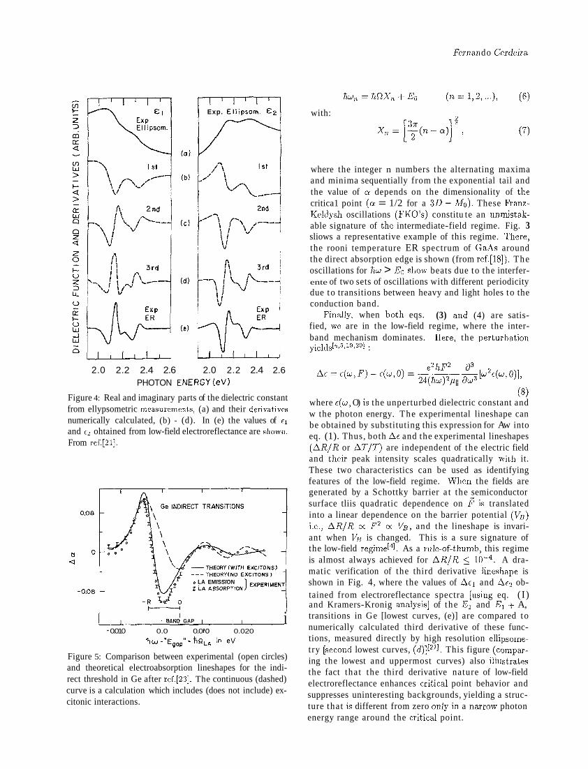
Figure 4: Real and imaginary parts of the dielectric constant from ellypsometric measurement,~, (a) and their deri~at~ives numerically calculated, (b) - (d). In (e) the values of €1
and tz ohtained from low-field electroreflectance are shown. From ref.[21].
THEOY (WITH EXCITONS)
b LA EMISSION
I I I BANO GAP I I i
- 0.010 0.0 0.0 1 o 0.020
h w - ' E ~ ~ ~ " + &R,, in e\/
Figure 5: Comparison between experimental (open circles) and theoretical electroabsorption lineshapes for the indi- rect threshold in Ge after ref.[23]. The continuous (dashed) curve is a calculation which includes (does not include) ex- citonic interactions.
with:
where the integer n numbers the alternating maxima and minima sequentially from the exponential tail and the value of a depends on the dimensionality of the critica1 point ( a = 1/2 for a 3 0 - Mo). These Franz- Keldysh oscillations (FKO's) constitu te an unmjstak- able signature of tlie intermediate-field regime. Fig. 3 sliows a representative example of this regime. TIiere, the rooni temperature ER spectrum of GaAs around the direct absorption edge is shown (from ref.[l8]). The oscillations for liw > Eo sliow beats due to the interfer- ente of two sets of oscillations with different periodicity due to transitions between heavy and light holes to the conduction band.
Finally, when botli eqs. (3) and (4) are satis- fied, we are in the low-field regime, where the inter- band mechanism dominates. I-Iere, the perturbation yields[4,5,19,201 :
(8) where t(w, O) is the unperturbed dielectric constant and w the photon energy. The experimental lineshape can be obtained by substituting this expression for Aw into eq. (1). Thus, both A6 and the experimental lineshapes (ARIR or AT/T) are independent of the electric field and their peak intensity scales quadratically witli it. These two characteristics can be used as identifying features of the low-field regime. When the fields are generated by a Schottky barrier a t the semiconductor surface tliis quadratic dependence on 9 is translated into a linear dependence on the barrier potential (VB) i.e., AR/R cc F~ cc Vg, and the lineshape is invari- ant when VB is changed. This is a sure signature of the low-field regime14]. As a rule-of-thumb, this regime is almost always achieved for AR/R < 10-4. A dra- matic verification of the third derivative lineshape is shown in Fig. 4, where the values of Aci and Ar2 ob- tained from electroreflectance spectra [using eq. ( I ) and Kramers-Kronig analysis] of the El and El $ A, transitions in Ge [lowest curves, (e)] are compared to numerically calculated third derivative of these func- tions, measured directly by high resolution ellipsome- try [second lowest curves, (d)]L2']. This figure (compar- ing the lowest and uppermost curves) also illustrates the fact tha t the third derivative nature of low-field electroreflectance enhances critica1 point behavior and suppresses uninteresting backgrounds, yielding a struc- ture tha t is different from zero only in a narrow photon energy range around the critica1 point.

Brazilian J o ~ r n a l of Physics, 1701. 23, no. 1, March, 1993 7
I I I . I I I I I I I I I . I
1.42 1.44 1.46 1.48 1.50 152 154 156 PHOTON ENERGY í e V )
Figure 6: Abs(1rption edge of GaAs at different tempera- tures after M. I). Sturge, Phys. Rev. 127, 768 (1962). Inset shows schematically the effed of electron-hole final-state in- teraction on suih an absorption edge.
In the vicinity of critica1 points, band energy dif- ferences can be substituted by a locally valid parabolic expansion. In this case, the dielectric function entering into eq. (8) can be approximated by[41201:
where m = -1/2,0 (logarithmic) and 112 are the re- sults valid for lD, 2D and 3D critica1 points. In eq. (9) A is a constant that is proportional to the square of the transitim matrix ekment and the phase factor 45 depends on the type of singularity (Mo, M1, Ma or ~ ~ ) [ ~ > ~ ~ 1 . Motlulation lineshapes can now be obtained by substitutin); this locally valid form of t into eq. (8) (intraband meihanism in low-field ER) or into eq. (2) (interband term in low- or intermediate-field ER or other form of rnodulation spectroscopy). Proceeding in this manner, a ~ d remembering the link between ARIR and A6 given in eq. (1)) experimental lineshapes ob- tained in low lield ER can be fitted by expressions of the type:
with n = 712,: or 5/2 for 113, 2D or 3D critica1 points. Values of E. and are easily obtained from these exper- imental lineshapes. Eq. (9) is valid for unconfined car- riers in a situa1 ion in which final state electron-hole in- teraction is neplected. In physical situations where this picture applies, additional information about the di- mensionality aiid singularity type ( M o , M1, M2 or M3) can be obtained from the values of m and O obtained from fitting experimental lineshapes with eq. (9). This information is, however, more uncertain since field inho- mogeneities and final state iilteractions produce drastic alterations in the values of these para meter^[^].
111.2 Final- S t a t e Electron-Hole Interact ions (Bulk Semiconductors)
Final-state electron-hole interaction (excitons) al- ters the one-electron picture described above. A general discussion of this subject is given by D O W [ ~ ~ ] . Closed form solutions cannot be obtained even in the simplest of cases. Numerical calculations for direct and indirect Mo absorption edges give a good description of experi- mental results for low- and intermediate-fields. A good example of this is the calculation of Weinstein, Dow and ao[^^] for tlie indirect electroabsorption of Ge (Fig. 5). The solid curve representing this calculation correctly describes the absorption edge and the FICO'S occurring at higher photon energies while the dotted curve (cal- culation without excitons) gives a poor description of tlie data and only reproduces the higher FKO's. Fig- ure 5 illustrates that even when the electron and hole are strongly correlated, intermediate fields still produce Franz-Keldysh oscillations. Surprisingly enough, the period of the correlated and uncorrelated cases is al- most the same for n 2 3 (the first few oscillations have shorter periods in the excitonic case), when the asymptotic expansion leading to eqs. (6) and (7) is valid[17>22T231
In the weak field limit it is sometimes possi- ble to find simple asymptotic expressions for hydro- genic excitons derived from the lowest direct Mo t r a n ~ i t i o n [ ~ ~ ~ ~ ~ ~ ~ I . When the exciton concentrates'most of the oscillator strength and its lifetime broadening is small enough, so that its absorption line is well sepa- rated from the band-to-band continuum, its contribu- tion to the dielectric constant can be obtained from eq. (9) by rn = -1. In this case, the in- terband mechanism is the correct one since the exciton is a neutra1 entity and is, therefore, not accelerated by the field. Hence experimental lineshapes would be ob- tained by inserting the dielectric constant of eq. (9) with m = -1 into eq. (2), which leads to a AR/R of the general form as that given in eq. (10) with n = 2. In this case E. would be the band-edge energy minus the exciton Rydberg and r the lifetime broadening of the hydrogenic exciton. In addition to generating bound states in the forbidden gap, the Coulomb electron-hole correlation greatly enhances the absorption cross sec- tion for photon energies above the gap[22], as shown schematically in tlie inset of Fig. 6. So, when r is large and the excitonic line is not well resolved from the enhanced continuum, the shape of the absorption edge changes from a square root ( a cc J-) to a step-like function characteristic of a 2 0 - Mo singu- larity. This is illustrated by Fig. 6, where the absorp- tion spectra of GaAs taken at different temperatures are displayed. As the temperature decreases so does r, and the atomic-like Lorentzian absorption of the exci- ton becames more marked and better separated from the continuum. However, the enhanced absorption and

8 Fernan do Cerdeira
step-like behavior of the latter can be observed at a11 temperatures. Hence, for the electric-field modulated absorption (or reflectivity), eq. (10) with n = 3 (third- derivative lineshape of a 2DMo singularity) also will fit the data in some cases where excitonic effects are im- portant. It is only in extreme cases that it can be de- cided by purely physical arguments whether this clioice is better or worse than n = 2 (first derivative of a sin- gle Lorentzian contribution by an isolated hyclrogenic exciton). In an intermediate case the linesliape will be well reproduced by both choices, which will yield the same value of Tlie value of r, however, is more dependent on our choice of n as are the other two ad- justable parameters ( C and 8) in eq. (10). Therefore, when trying t o ascribe physical significance to C, 8 and sometimes even r, care must be taken to a~cert~ain that our choice of n reallr describes the physical conditions of the experiment.
The above discussion can be summarized by saying that, if we are in the low-field limit, eq. (10) is useful in a11 practical situations that involve bulk semiconductors (whether excitonic effects are important or not). Use of this lineshape to fit experimental spectra yields good values of transition energies (Eo) and, in most cases, lifetime broadenings. When extreme care is Laken to fit the choice of n to the actual physical situation, in- formation about singularity type also can be obtained from the phase factor (8). The amplitude C is gener- ally of use when testing selection rules, comparing lines arising for different transitions in the same spectrum or following the dependence of this parameter in a given line as a function of an externa1 perturbation (stress, external-applied fields, et
111.3 Applicat ions t o Semiconductor Microstruc- t u r e s
When applying the results described above to semi- conductor microstructures, care must be taken to as- certain that the assumptions that led to the lineshape equations such as eqs. (8) to (10) are still valid. In some of these structures the carriers are confined in the direction of the modulating field. Such is the case of single qnantum wells (SQW) or multiple quantum wells (MQW), separated by large barrier regions, with the modulating field along the growth axis. In these cases, carriers cannot be accelerated by the field and the intraband term, which leads to third-derivative line- shapes, does not contribute to A&. Although there have been reports to the effect that experimental line- shapes in MQW's are well described by TDLS of 2 0 - critica1 points[26-29], this may not be physically mean- ingful. It is true that the joint density of one-electron states is a step function ( 2 0 - Mo), but since the field is applied along the direction of confinement it does
not accelerate the carriers (intraband term) and pro- duces no third-derivative terins in Ar. This is com- pounded by strong evidence that in tliese structures excitonic interactions are of great importante even at room t e n ~ ~ e r a t u t e [ ~ ~ - ~ ~ ] . Thus, low-field ER from these confined systems should produce first derivative lineshapes (FDLS), with Ar given by eq. (2). In ap- plying this equation, however, one must first deter- mine the appropriate form of E . The subject was re- cently discussed by Glembocki and S h a n a b r ~ o k P ~ ~ ~ ~ ] , who study the ER and PR spectra of some MQW's of AlGaAs/GaAs at temperatures ranging from G I< to room temperature. The lowest temperature PR spectra are compared to pliotoluminescence excitation (PLE) results. Tliis comparison shows that the PR line arises from electric-field modulation of an excitonic transi- tion and that both its transition energy and lifetime broadening are well described, at low temperatures, by a first-derivative lineshape of a Lorentzian (hydrogenic) excitonic contribution to E, i.e., eq. (10) with n = 2. For temperatures T > 150K, however, FDLS of a di- electric function with a Gaussian profile gives better fit to tlie data[36]. The Gaussian nature of excitonic ab- sorption lines may arise under a variety of conditions, including strong exciton-phonon coupling (as in high temperatures) inhomogeneous perturbations and rough interfacedg]. It is to be noted, however, that these lines are aIso well reproduced by TDLS of a 2D-critical point [eq. (10) with n = 31. This fit yields the same value of E0 as the FDLS of a Gaussian €2 , albeit consider- ably different values of r. The authors of references [35] and [3G] believe this to be fortuitous. However, the evidence in favor of Gaussian excitonic absorption is mostly empirical. ~ s ~ n e s [ ~ ~ l suggests that the only pre- requisite for obtaining TDLS may be that the carrier (electron or hole) acceleration by the field has actual physical meaning. In a QW, motion along tlie field (z) direction corresponds to transitions between subbands. When high temperatures or rough interfaces make in- tersubband separations of the same order of lifetime broadenings, the field, however weak, may easily mix wavefunctions of different subbands which, in semiclas- sical terms, has the effects of acceleration along the 6eld direction. This situation is far more common tlian can be at first imagined if instead of thinking about electrons, we focus our attention on heavy holes, which have larger effective masses and are subject to shaI- lower confining potentials in most microstr~ctures[~~]. In this case, the appropriateness of using TDLS of 2D singularities (since the electrons are still confined in the z-direction) gains physical significance. Another situa- tion in which TDLS might be appropriate is when there is sufficient overlap between the wavefunctions of car- riers confined in different QW's, so that field-induced tunneling between wells is possible. The degree of over- lap is determined by the width of the barriers, the depth of the QW's and the order of the confined level; con-

Brazilian Jcurnal of Physics, vol. 23, no. I, March, 1993
fined states 3f large quantum numbers lie closer to the edge of the c uantum well, producing larger overlap and larger lifetinie broadenings. An extreme case would be that of a true superlattice, when confined levels evolve into continuous minibands of width A 10 - 50 meV « r. In these cases the :;tates are truly 3D, but with a m a s consiierably larger along the z-direction, which might lead tcg TDLS of approximately 2D-critica1 points even in the resence of excitonic effects.
Another 3oint under discussion is whether in such systems, full understanding of the spectrum can be achieved by lerivatives OS locally-valid dielectric func- tions based o 1 expansions in terms of localized van Hove singularities, especially when final-state electron-hole correlations are taken into account. This picture may break down when these singularities have an energy spacing smaller than, or of'the order of, some other sig- nificant ener(;ies in the problem, such as miniband en- ergy spread (A), the exciton binding energy (E,,,), the lifetime broatlening of the one-electron state (r) or the typical energy that a carrier may gain from the acceler- ating electric field (hR). Recent calculations for SQW's show that evm when tunneling along the field direc- tion is not possible, intersiibband mixing and subband dispersion in the xy-pIane (I to the field and confin- ing directions) produce features in the ER spectra that cannot be predicted by a critica1 point a n a ~ ~ s i s [ ~ ~ ] .
The discussion above shows that the question on the appropriate lineshape to be used in fitting experi- mental spectrs of electric field modulated reflection or absorption is hoth complex and not completely settled. As a rule-of-tliumb, TDLS of 2D singularities [eq. (10) with n = 31 seem to give good overall-fits of frequently encountered si tuations. The same can be said of FDLS of Gaussian profiles. Both fittings give reliable values of Eo, but in order to ascribe physical significance to the other parameters resulting from the fit, a good un- derstanding of the actual physical situation is required.
N. Recent ILesults
IV.l. Low F:ield Regime
In the conciitions of lovv fields [eqs. (3) and (4)], structures in the photornodulated spectra of QW's, MQW's and superlattices originate in transitions be- tween hole and electron subibands. These subbands can generally be cdculated (in direct band-gap materials) with variation:s of a simple Kronig-Penney m~del[~'] based on the Sact that the different gaps of the con- stituent materials generate, for a free carrier in the effective-mass approximation, a periodic square well structure. To describe this potential the band align- ments on both sides of the heterojunction must be known. Hence, one of the most important results of this type of spertroscopy is to determine the band align- ments in differcnt heterojunctions. Another important question is de.,errnining the degree of spread of the
states produced by this periodic potential as a func- tion of coupling between neighboring quantum wells. Finally, the validity of this simple description might be questioned, especially in cases where the bulk con- stituents do not have direct gaps. Modulation spec- troscopy has contributed, and still contributes, to find answers to these questions. In what follows we illustrate this using as examples photo and electromodulated re- Aection and absorption work performed in our labora- tories in two strained-layer systerns: InGaAs/GaAs and Ge/Si quantum wells and superlattices.
I V . l . l Tl ie In,Gal-,As/GaAs Sys tem
Strained-layer In,Gal-,As/GaAs superlattices have been extensively studied by optical t e ~ h n i ~ u e s [ ~ ~ I . In this system, the electronic states of interest are to- tally or partially confined within the alloy material. Hence, the large portions of the sample that constitute the substrate, buffer and capping layers are made up of GaAs and are transparent in the photon energy range of interest. This allows spectroscopic measurements to be performed in transmission, rather than in reflection, which has the advantage that a11 the contributions to the observed spectra come from the region of the sam- ple containing the microstructures under study, since the sample became opaque when the absorption edge of GaAs is reached. On the negative side, the confined states are broadened by such effects as the random po- tential of the InGaAs alloy and the inherently rougher interfaces which occur in strained-layer superlattices, even in the absence of strain relaxation. Even so, the study of directL4l] and photomodulated transmission['l has given important insights into the electronic prop- erties of microstructures based on this type of hetero- junctions.
(i) B a n d Alignment
. One of the most important questions about this sys- tem is the value of the offset parameter Q , defined as
Q = A&
AE, + AE,HH '
where AE, and A E ~ ~ are the conduction and heavy hole valence band discontinuities, respectively. The large splitting between light- and heavy-hole valence bands produced by biaxial strain results in a different potential profile for each type of carrier. For some values of Q(Q > 0.6) it is possible to confine light holes in the GaAs layers while both electrons and heavy holes are confined in the lower energy gap alloy lay- ers. Accurate determination of this parameter, how- ever, proved to be a difficult task. Light scattering e ~ ~ e r i m e n t s [ ~ ~ ] suggested Q 2 0.4, while other op- tical techniques yielded values of Q between 0.6 and 0.8[43-491. In an attempt to reconcile this diversity of values, Joyce et a1.L5'1 suggested that the value of Q
Brazilian Journd of Physics, voI. 23, no. 1, March, 1993
might depend on the Indium molar fraction, x, taking values of Q 0.4 for low molar fractions and increasing
to Q Y 0.8 as molar fraction increased. This assump- tion received some support from PR rnea~uremen td~~] performed on two In,Gall-,As/GaAs samples of x = 0.19 and x = 0.45. More recently, Vázquez-López et al.['] performed a systematic study of this system us- ing photomodulated reflectance and transmission. In
their study they used a collection of InxGaí-,As/GaAs
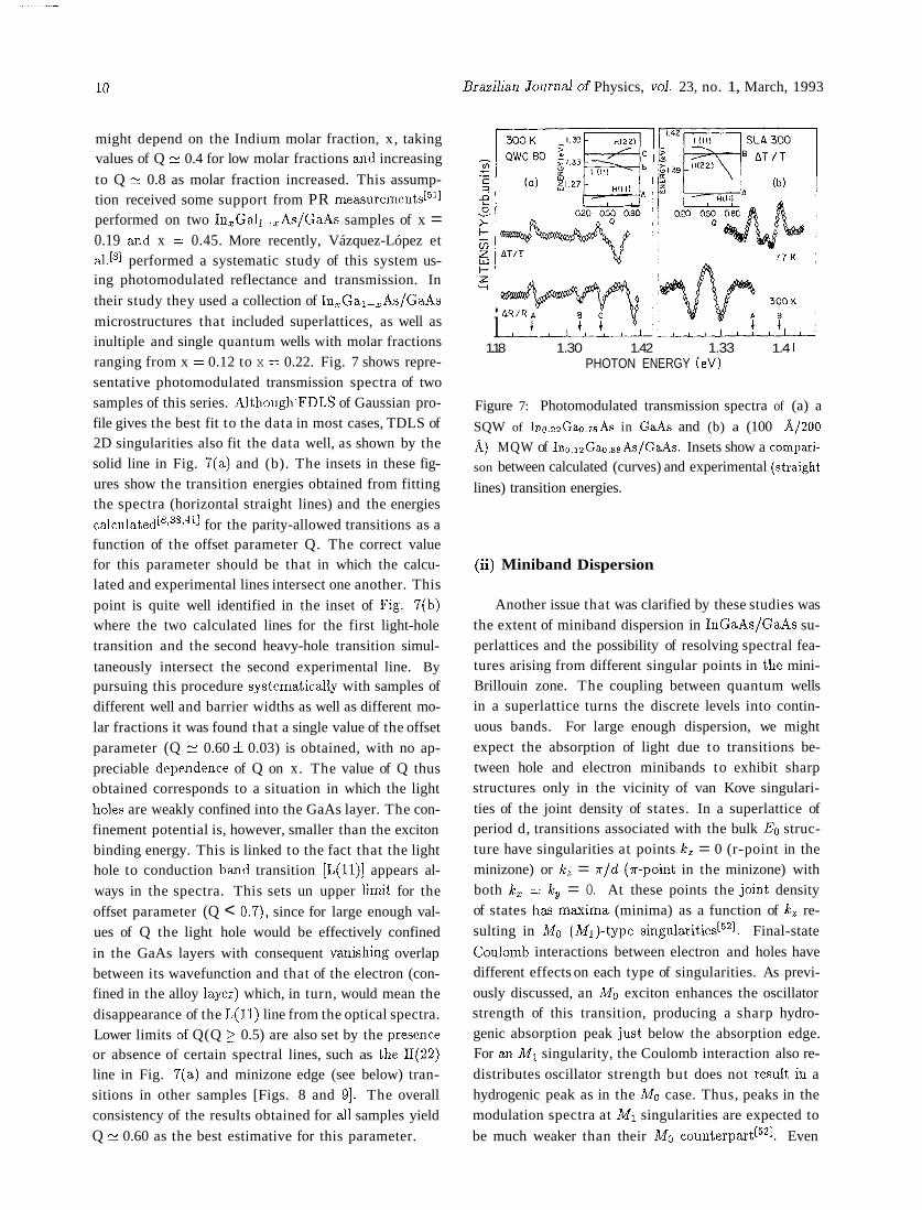
microstructures that included superlattices, as well as inultiple and single quantum wells with molar fractions ranging from x = 0.12 to x = 0.22. Fig. 7 shows repre- sentative photomodulated transmission spectra of two samples of this series. Although'FDLS of Gaussian pro- file gives the best fit to the data in most cases, TDLS of 2D singularities also fit the data well, as shown by the solid line in Fig. 7(a) and (b). The insets in these fig- ures show the transition energies obtained from fitting the spectra (horizontal straight lines) and the energies
c a l c ~ l a t e d [ " ~ ~ ~ ~ ~ I for the parity-allowed transitions as a function of the offset parameter Q. The correct value for this parameter should be that in which the calcu- lated and experimental lines intersect one another. This
point is quite well identified in the inset of Fjg. 7(b) where the two calculated lines for the first light-hole transition and the second heavy-hole transition simul-
taneously intersect the second experimental line. By pursuing this procedure systematically with samples of different well and barrier widths as well as different mo-
lar fractions it was found that a single value of the offset parameter (Q Y 0.60 0.03) is obtained, with no ap- preciable dependence of Q on x. The value of Q thus obtained corresponds to a situation in which the light
holes are weakly confined into the GaAs layer. The con- finement potential is, however, smaller than the exciton binding energy. This is linked to the fact that the light hole to conduction band transition [L(11)] appears al-
ways in the spectra. This sets un upper lirnit for the
offset parameter (Q < O.7), since for large enough val- ues of Q the light hole would be effectively confined
in the GaAs layers with consequent vanisliing overlap between its wavefunction and that of the electron (con- fined in the alloy layer) which, in turn, would mean the
disappearance of the L(11) line from the optical spectra. Lower limits of Q(Q > 0.5) are also set by the presence or absence of certain spectral lines, such as the H(22) line in Fig. 7(a) and minizone edge (see below) tran- sitions in other samples [Figs. 8 and 91. The overall consistency of the results obtained for a11 samples yield
Q Y 0.60 as the best estimative for this parameter.
i 1.18 1.30 1.42 1.33 1.4 1
PHOTON ENERGY (eV)
Figure 7: Photomodulated transmission spectra of (a) a
SQW of Ino.22Gao.78As in GaAs and (b) a (100 A/200 A) MQW of Ino.izGao.ssAs/GaAs. Insets show a compari- son between calculated (curves) and experimental (straight
lines) transition energies.
(ii) Miniband Dispersion
Another issue that was clarified by these studies was the extent of miniband dispersion in InGaAs/GaAs su- perlattices and the possibility of resolving spectral fea- tures arising from different singular points in tlie mini- Brillouin zone. The coupling between quantum wells in a superlattice turns the discrete levels into contin- uous bands. For large enough dispersion, we might expect the absorption of light due to transitions be- tween hole and electron minibands to exhibit sharp structures only in the vicinity of van Kove singulari-
ties of the joint density of states. In a superlattice of period d, transitions associated with the bulk E. struc- ture have singularities at points k , = 0 (r-point in the minizone) or k , = n/d (r-point in the minizone) with both k , = ky = O. At these points the joint density of states has maxima (minima) as a function of k , re- sulting in Mo (M1)-type s ing~lar i t i es [~~] . Final-state
Coulomb interactions between electron and holes have different effects on each type of singularities. As previ-
ously discussed, an Mo exciton enhances the oscillator strength of this transition, producing a sharp hydro- genic absorption peak just below the absorption edge. For an Ml singularity, the Coulomb interaction also re-
distributes oscillator strength but does not resuIt in a hydrogenic peak as in the Mo case. Thus, peaks in the modulation spectra at Mi singularities are expected to
be much weaker than their Mo ~ o u n t e r ~ a r t [ ~ ~ 1 . Even

Fernando Czdeira
worse, since the energy separation between both singu- larities (A) inight be of the order of the binding energy of the Mo h'rdrogenic exciton (E,,,) the redistribution of oscillator titrength produced by the 1att.er might oblit- erate the coiltribution of the M1 singularity to the ab- sorption spectrum (i.e., ~~avefunction from the whole miniband might enter the formation of a single hydro- genic excitor.). Even if Coulomb interactions were not important, tliese two singiilarities could not be resolved if A was not much larger than the lifetime broadening of one-electron states (I'). Hence, the observability of two distinct :;pectral lines in the modulated absorption spectra, arising from the two singular points and n on the minizone, depends on A being larger than r and (E,,,(. Typical values of these quantities are r - 1 - 7 meV and IE,!lel 10 meV. Hence, we would expect to see manifejtations of the rniniband dispersion in the optical spect:.a for A > 20 meV. Such manifestations were reporterl by Slien et a1.[531 for AlGaAs/GaAs su- perlattices ar d by Ribeiro et al.L9] and Vázquez-López et al.181 for InGaAslGaAs superlattices.
In figure :{(a) the 77 1: photomodulated transmis- sion spectruni of a 100 A-period superlattice made up of equal layer thickness of Ino i6Gao a4As and GaAs is shown (ref [a]). The solid line represents a fitting with an FDLS of a Gaussian absorption profile. Three transitions [aprows in Fig 8(a)l are needed to fit the spectra: two strong ones ( A and C) and a weaker one (B) to accourit for the shoulder in the higher energy side of line A. The necessity of including the latter is illustrated by the dashed line, which represents a fit where this we;~k transition is ornitted. The inset in Fig. 8(a) shows the parity-allowed transitions calculated as a function of t le offset parameter (curves) and the tran- sition energies (straight horizontal lines) obtained from fitting our spectrum. The electron and heavy-hole mini- bands, from ~vhich these transitions were calculated (Q = 0.60), ar: shown in Fig. 8(b). The stronger peaks in the spectruin (A and C) are assigned to the Mo sin- gularity at the zone center due to transitions from both light- and heavy-hole valence-band states to the only electron minib md. Line B appears in a region where no transitions occur at the center of the minizone. Its posi- tion is in the níbighborhood of the (Ml) saddle point sin- gularity occurring at the edge of the minizone (r-point). A similar shoulder is observed in the photoreflectance spectrurn of a 00 A-p eriod AlGaAsJGaAs superlattice by Çhen et al.[j3] and is also attributed to a transition at the r-point of the minizone. These authors point out that the rrodulation produced by the electric field at the r- and n-points has opposite phase. Our fittings result in a phat e for line B which is opposite to those of lines A and C. Also, the zone center Mo and the zone edge Ml singulsrities should be separated by an energy of 33 meV [Fi!;. 8(b)]. T h ~ l energy separation of our spectral featurcs is 25 f 4 meV. This agreement is very good when conjidering that the calculated energy sep-
aration does not take into account excitonic effects and that this separation is very sensitive to small fluctua- tions in the superlattice period d [shaded area in inset of Fig. 8(a)].
1 -I 00- \ .34 1.40 \ .46
o n/d Kz
PHOTON ENERGY (eV)
Figure 8: (a) Photomodulated transmission of a 100 A period Ino,l~Gao.~~As/GaAs superlattice with equal al- loy/GaAs thickness and twenty repetitions; (b) Miniband dispersion calculated for Q = 0.60.
Another example is given in Fig. 9(a) which shows the AT/T spectrum of a 200 A- period superlattice made up of equal layer thickness of Ino,izGao ssAs and GaAs at 77K. The calculated minibands (Q = 0.59) are shown in Fig. 9(b). The spectrum is fitted (con- tinuou~ line) in the manner previously described with five transitions, labelled A, B, C, D, and E, in order of increasing energy indicated by arrows in Fig. 9(a). These are shown in the inset of Fig. 9(a) as horizontal straight lines, while the curves represent the energies for the various possible transitions arising from the theo- retical miniband scheme [Fig. 9(b)] as a function of Q. The assignment of lines A to C as well the choice of Q = 0.59 for the offset parameter are discussed in ref. [8]. Here we shall be concerned only with the assign- ment of lines D and E. They are both relatively strong and well defined lines that cannot be attributed to any allowed or forbidden zone-center transitions. Fig. 9(b) shows that the second electron rniniband is strongly dis- persive, having a minimum at the minizone edge and in- creasing its energy with decreasing wavevector in such a way that it merges into the continuum before it reaches the minizone center. Since the first and second heavy- hole minibands are virtually dispersionless, transitions from these bands into the second conduction miniband at the zone edge would give rise to Mo singularities in the joint density of states. In contrast, these same tran- sitions at the zone center should not contribuie lo the


Fernando Cerdeira
r- Without band ( b ) T = 77K ( 0 ) With bãnd \~ ( C )
non-paiabolicities non parabolicities ........................................................................... H - ---) .................................................................... .......................................................................... ....... -- C- - ........................................................... 4h _---
31 C \
____------ '\
...........................
Figure 10: (a) Photoreflectance spectrum of a Ge/Geo,.rSio.a (1.11 A/ 32 A) x 20 superlattice. Arrows indicate the transition energies obtair.ed from a FDLS of a Gaussian absorption profile. Comparison with calculated minizone center (edge) transi- tions are given as continuous (dashed) curves in (b) with constant effective masses and (c) with energy dependent effective masses.
SinGem thin layer ~ u ~ e r l a t t i c e s [ ~ ~ ] . However, quantita- tive comparism between calculated and experimental energy transitions, where it was possible (ref. [74] and [75]), differs by as much as 110 meV.
A recent photoreflectance study performed on Ge/Geo 7Sio 3 superlattices by Rodrigues, Cerdeira and ~ean["] shous that these discrepancies can be ex- plained without invoking rnixtures of bulk r, X and L states if band non-parabolicities are taken into ac- count. Fig. 10(a) shows a representative PR spec- trum in the ~thoton energy region of 0.95 - 1.70 eV. The authors identify the lines in this spectral region (A to H in o-der of increasing energy)as originating in transitions between confined superlattice states de- rived from bu k Ge r-point states. The identification is made in a rnanner similar to that explained in sec- tion IV.l.l(i). First, a calculation is made with a sim- ple scalar version of a ~ r o n i ~ - ~ e n n e ~ [ ~ ' ] model, using zone-center bulk states and constant carrier masses, as a function of i,he discontinuity of the average valence bands (AEtu ) [60]. The results of these calculations are shown in I'ig. 10(b) as a solid (dashed) curves for parity allowed transitions at the minizone center (edge) while experimental transition energies are represented in this figure by horizontal dotted lines. Agreement hetween calculited and measured transition energies is poor, regardless of the value chosen for A E i u , for a11 but the lowest energy lines in the P R spectrum. The origin of these discrepancies (as well as those reported by other authcrs) can be uriderstood if we notice that
confinement energies in these systerns can have values considerably larger than that of the E. transition in bulk Ge. This should produce strong dependence of the carrier effective mass on the confinement index n. Taking these non-parabolicities into account, Rodrigues et al.[141 used the same model to recalculate the transi- tion energies. Now, excellent agreement is obtained for a band offset of AE,"" = 0.14 f 0.03 (Q = 0.73 rt 0.03), as can be seen in Fig. 10(c). Hence, the use of PR has demonstrated the validity of treating these transi- tions in terrns of bulk r-point bulk-Ge states, shown the importance of band non-parabolicities in the case of deep potential wells and deterrnined the band-offset parameter for the Ge/Ge,Sil-, interface.
The validity of using a simple Kronig-Penney type model in the Ge/Si system is the most striking of the re- sults described above. Still, this was demonstrated for a superlattice with a relatively large period (d E 140 A). The nagging question remains as to whether the same woiild be true for the very thin superlattices ob- tained by alternating layers of Si and Ge, each only a few monolayers t h i ~ k [ ~ ~ ] . Figure 11 shows ER spectra of three GenSim superlattices, where n (m) is the num- ber of monolayers of Ge (Si) in each period of (n+m)- thickness. Determination of the E. optical transition in these samples is not always easy. In thin samples, such as Ge5Si5 (upper curve in Fig. 11), interference patterns mask the ER line. However, using the method suggested by Garriga et al.[76] a good estimate of the transition energy is obtained. In thicker samples, as in

14 Brazilian Journal of Physics, vol. 23, no. 1, March, 1993
the Gei6Sii6 (lower curve in Fig. ll), a strong ER line associated with defect formation appears just below the direct absorption and hinders the observation of the E0
structure. The middle curve shows an ER spectrum (Ge8Si12) in which this structure is clearly observed. In this case the transition energy can be unambiguously obtained from a fitting with a TDLS for 2D singularity. The values thus obtained from these spectlra coincide within 0.1 eV with the predictions of a non-parabolic three-band model. For the thinner sample this pre- diction also coincides with that of more sophisticated LMTO ca l~ula t ions[~~] . These results suggest that the non-parabolic three-band model retains its predictive value for the direct gap even down to superlattices of only ten monolayers in thickness. Figure 11 also shows a complex of structures (delimited by the vertical solid and dashed lines) at higher photon energies. TIiese can be associated with the Ei transitions in t,he siiperlat- tice. No simple model has yet been developed to un- derstand these s t r u c t u r e ~ [ ~ ~ I . In spite of the surprising result concerning the E. transitions in these siiperlat- tices, the full understanding of their ER spectra calls for further work.
1 0 1.5 % O 3 5 3 0 3 5 Ptio Lori Ericrg,v (?V)
Figure 11: ER spectra of Ge,Si, superlattices. Arrows in- dicate the value of E0 calculated with Kronig-Penney model [Eo(KP)] and those obtained from experiment. The shaded photon energy region contains structures related to bulk E1
transitions.
IV.2 In t e rmed ia t e and High-Field R.egimes
So far we have Iimited our discussions to resuIts ob- tained in the low-field regime, where the spectral fea- tures are interpreted in terrns of intersubband transi- tions. As discussed in section 111, the absorption coef- ficient shows marked changes when fields exceed those
imposed by the criteria of eqs. (3) and (4). In bulk semiconductors it would be difficult to obtain an elec- tric field high enough that would take the problem into the high-field regime. Here the effective-mass approxi- mation can be used and the eigensta.tes in the presence of the field are Airy functions, which are delocalized and have a continuous energy spectrum. Transitions between these eigenstates produce an absorption coef- ficient with an exponential tail at photon energies be- low the absorption edge and oscillations above it with periodicity given by eq. (6). This process was dis- cussed in section 111.1 and is pictorically illustrated in Fig. 12(a). Our ideas about these effects must be revised when applied to semiconductor microstruc- tures. The closer spacing bet,ween subbands and the smaller subband dispersion in semiconductor superlat- tices can create the conditions for achieving Iiigh-field regimes with moderate electric fields. Such conditions have allowed the observation of Stark-Wannier ladders in the photo-conductivity and electroreflectance spec- tra of A1,Gal-,As/GaAs ~u~erlattices~~"-". In these cases tlie intermediate-field regime proved to be more difficult to identify and was only recently reported by Cadeira et a1.[l0]. On the other hand, this regime might talte an entirely different form when only one type of carrier can be accelerated by the electric field, while the other is confined by the microstructure po- tential along the field direction. Such a situation, il- lustrated in Fig.l2(b), would occur in the 2D-electron gases confined in modulation-doped heterojunctions or in the V-shaped potential of GaAs samples with Si-& doping, and might result in a quantum-confined ver- sion of the F'ranz-Keldysh effect. These two cases shall be discussed in tlie following two subsections. When studying these cases it must be kept in mind that the fields which alters the electronic wavefunctions are externally-applied dc-fields or the interna1 fields created by the microstructure (as in the 2DEG). The modulat- ing ac-fields are small and constitute a perturbation on the dc-field.
IV.2.1. InxGai-,As/GaAs Superlat t ices
We already saw that the conditions for Franz- Keldysh oscillations are almost always satisfied in bulk direct-gap semiconductors. In order for these oscilla- tions to appear in the spectrum, with the periodicity of eq. (6) (i.e., period proportional to F ~ / ~ ) , two things are necessary: that the electric field be small accord- ing to the criterium of eq. (3) and that the effective mass approximation be valid. The first condition in- sures that the dominant mechanism of interaction be- tween the field and the carrier is the intrahand acceler- ation by means of which it gains a typical energy of the order eFd (d is the period of the lattice along the field direction). The second is insured by requiring that, in gaining this energy, the carriers do not stray too far from the extrema, when a parabolic expansion of the
Fernando Cer deira
: a ) BULK (b ICONF I NED
Figure 12: Schcmatic representation of the optical transitions that lead to the Franz-Keldysh effect in the absorption edge of a direct gap semiconductor in (a) bulk and (b) the space-charge region of a modulation doped heterojunction.
a AT/ T 0=0.57
SLA i 00 2 77 K H(2 1)
W 1.40 1.45
PHOTON ENERGY ( e V 1
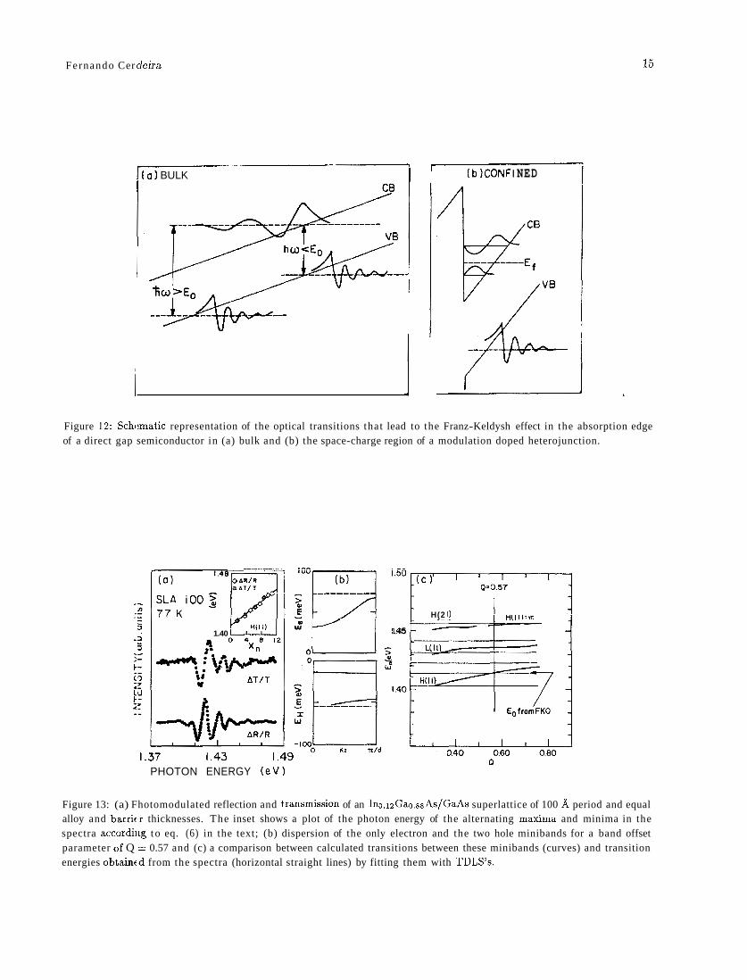
Figure 13: (a) Fhotomodulated reflection and transmission of an Ino.i~Gao.ssAs/GaAs superlattice of 100 A period and equal alloy and barricr thicknesses. The inset shows a plot of the photon energy of the alternating maxima and minima in the spectra accordiig t o eq. (6) in the text; (b) dispersion of the only electron and the two hole minibands for a band offset parameter of Q = 0.57 and (c) a comparison between calculated transitions between these minibands (curves) and transition energies obtaincd from the spectra (horizontal straight lines) by fitting them with TDLS's.

16 Brazilian Journal of Physics, vol. 23, no. 1, March, 1993
energy band in terms of some effective mass is Iocally valid. This is more or less equivalent to requiring that the acceleration energy (eFd) be very small in terrns of the width of tlie energy band (A), i.e.:
where the dimensionless quantity f is often referred to as the "effective electric field" . As f approaches unity, the wavefunction of the carrier becomes local- ized on a length scale X E d/f. When this happens, the effective-mass approximation is no longer valid and the coupling between states in different unit cells along @ decreases. Here a tight-binding approach is a better starting point for discussing the problem. For f > 1 these states become totally decoupled and the resulting regime is known as that of Stark-Wannier localization. The absorption coefficient in this case would show a se- ries of equally spaced (neFd; n = 0 ,51 , &2, ...) peaks known as Stark-Wannier ladders (SWL's). Although the conditions for achieving this regime are difficult to meet in bulk serniconductors (d E 6A, A - 1 eV), in a superlattice both bandwidths and periods can be tailored to obtain f - 0.1 at relatively modest fields (F - 104 - 105 V/cm). Following the first reports of SWL f o r m a t i ~ n [ " ~ ~ ~ I , the high-field regime in semi- conductor superlattices has been studied with a va- riety of techniques by different a ~ t h o r s [ ~ " ~ ~ @ ] . The intermediate-field regime for these materials, however, has not been very well studied. To the best of our knowledge, the first report of FKO in a semiconductor superlattice is that of Cerdeira et al.[lO]. These authors studied the photomodulated reflection and absorption spectra of an In,Gal-,As/GaAs superlattice with a built-in field of F E 7 kV/cm and found an oscillatory structure, which can be unambiguously attributed to FKO's. Photomodulated reflection (ARIR) and trans- mission spectra of this sarnple (d = 100A, z = 0.12) are displayed in Fig. 13(a), while the minibands of the superlattice are shown in Fig. 13(b). We first notice that the shape of the AR/R and AT/T spectra bear the unmistakable signature of FKO's associated with a 3D absorption edge. This is appreciated when compar- ing Fig. 13(a) with Fig. 3. Second, if we tried to fit the spectra with third or first derivative lineshapes we would need 6 transitions [horizontal lines in Fig. 13(c)] which cannot be explained by intersubband transitions for any value of the band offset parameter, as shown in Fig. 13(c). Finally, when plotting the energy positions of the alternating maxima and minima according to eq. (G), we obtain a straight line [inset of Fig. 13(a)] which yields F E 7 kV/cm (slope) and E. = 1.414 eV (inter- cept) for the absorption edge. This value of E. corre- sponds to the calculated absorption edge for Q = 0.57 [see Fig. 13(c)], in accordance with the results for many other samples of this type discussed in section IV.l. l . Hence, the results of Fig. 13 can a11 be consistently ex-
plained by the existence of a built-in dc-field of F E 7 kV/cm. The existence of this field regime is not by any means obvious. In the case under consideration (d = 100A, A = 37 meV) eq. (12) is satisfied since the built-in dc-field mentioned above yields f E 0.2. On the other hand, the heavy-hole miniband has a negligi- ble dispersion (Ah 2 1.5 meV) which means that this hoIe is completely localized by the field (fh E 5). The electron-hole interaction, if strong enough, could now localize tlie electron as well if the externa1 field is weak enough, i.e., if
eFao K IEexcl (2)
when ao is the exciton radius. Hence, the field must satisfy two simultaneous requirements:
eFao 2 lEeXcI and eFd « A. (3)
In the case under discussion (with ao E 150 -4 and IEe,,l E 4 meV) condition (14) is satisfied, but in a general case the appearance of FKO's depends on a delicate balance between field strength, exciton ra- dius, superlattice period, exciton binding energy and miniband spread (A). The observation of this effect is also made difficult in most superlattices, such as AlGaAslGaAs, because the signal from the superlat- tice may be masked by oscillatory behavior originating in the bulk portions of the sample (substrate, buffer and capping ~ a ~ e r s ) [ ~ ~ ] . Transmission measurements performed in InGaAs/GaAs superlattice contain infor- mation ONLY from the superlattice region since the sample becomes opaque when the absorption edge of GaAs (which constitutes the bulk parts of the sarnple) is reached.
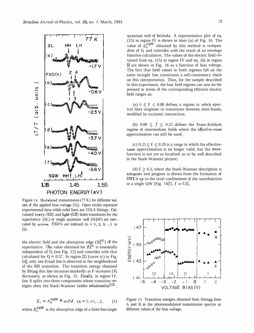
Once the existence of the Franz-Keldysh regime for this superlattice is established, the evolution of the spectra as a function of the electric field can be studied by sandwiching it between nf and p f GaAs layers and varying the electric field by applying a bias voltage (g) to this sandwich. Such experiment is reported in ref.1131 and representative modulated transmission spectra for different values of Vb are displayed in Fig. 14. Four bias-voltage regions (I to IV in order of decreasing h, i.e., increasing dc-electric field) are easily identifiable in these spectra. In region I [curve (a) in Fig. 141 the field is very weak and the spectra correspond to that of excitonic lineshapes (FDLS of a Gaussian absorption profile). The two structures which appear in the spec- tra (labelled A and B) of this field region correspond to minizone-center transitions between heavy-(HH) and light-(LH) hole states to the only conduction rniniband. These transition energies remain unaltered throughout this field region (see Fig. 15) and they coincide with those calculated by the envelope-function method with Q = 0.57. In region I1 we are in the intermediate or Franz-Keldysh regime [curve (b) in Fig. 141. By plot- ting the positions of alternating maxima and rninima according eq. (6) [see inset in Fig. 161, we obtain both
Brazilian JOL rnal of Physics, vol. 23, no. 1, March, 1993
1.3 5 1.45 1.55 PHOTON ENERGY (eV)
Figure 14: Modulated transmission (77 K) for different val- ues of the applied bias voltage ( V b ) . Open circles represent experimental data while solid lines are TDLS fittings. Cal- culated heavy-IHH) and light-fLH) holes transitions for the superlattice (SL) or single quantum well (SQW) are indi- cated by arroms. FKO's are indexed (n = 1, 2, 3, ...) in
(b).
the electric field and the absorption edge of the superlattice. The value obtained for ~t~ is essentially independent o € 6 (see Fig. 15) and coincides with that calculated for Q = 0.57. In region I11 [curve (c) in Fig. 141, only one Eroad line is observed in the neighborhood of the HH transition. The transition energy obtained by fitting this line increases markedly as F increases (E decreases), as shown in Fig. 15. Finally, in region IV, line A splits into three components whose transition en- ergies obey the Stark-Wannier ladder r e l a t i~nsh i~ [ '~ ] :
E, = + neFd (n = O, f 1, ...), (1)
where ~f~~ is the absorption edge of a field-free single
quantum well of InGaAs. A representative plot of eq. (15) in region IV is shown in inset (a) of Fig. 16. The value of ~t~~ obtained by this method is indepen- dent of 6 and coincides with the result of an envelope function calculation. The values of the electric field ob- tained from eq. (15) in region IV and eq. (6) in region 11 are shown in Fig. 16 as a function of bias voltage. The fact that field values in both regimes fall on the same straight line constitutes a self-consistency check on this interpretation. Thus, for the sample described in this experiment, the four field regions can now be ex- pressed in terrns of the corresponding effective electric field ranges as:
(a) O L f < 0.08 defines a regime in which spec- tral lines originate in transitions between mini-bands, modified by excitonic interaction;
(b) 0.08 < f < 0.21 defines the Franz-Keldysh regime of intermediate fields where the effective-mas approximation can still be used;
(c) 0.21 < f 5 0.29 is a range in which the effective- m a s approximation is no longer valid, but the wave- function is not yet so localized as to be well described in the Stark-Wannier picture;
(d) f > 0.3, where the Stark-Wannier description is adequate and progress is shown from the formation of SWL's up to the total confinement of the wavefunction in a single QW [Fig. 14(f), f = 0.51.
-5 -4 -3 -2 - 1 o 1 2 VOLTAGE B I AS (V)
Figure 15: Transition energies obtained from fittingg lines A and B in the photomodulated transmission spectra at different values of the bias voltage.

Fernan do Cerdeira
B I A S V O L T A G E ( V )
Figure 16: Electric fields obtained from eqs. (6) (region 11) and (15) (region IV) in the text (open circles). The straight line is a linear regression fit to these points. Inset shows application of eqs. (6) and (15) to the calcula.tion of F.
Wliile the above results may not be universally valid, this step-by-step evolution of the electronic states as a function of the field constitutes a powerful starting point to a more complete understanding of the subject than was previously available.
IV.2.2. Two-Dimensional Electron G a s
The intense electric field which confines a two- dimensional electron gaç (2DEG) in some semiconduc- tor microstructures such as a modulation doped het- erojunction (MDHJ) or GaAs samples with Si 6-doping may lead to a situation such as shown in Fig. 12(b), where the electrons are confined in quantized subbands while the holes are freely accelerated by the field. When the potential is narrow and only a small number of subbands exists, a quantum mechanical version of the Franz-Keldysh effect might take place. The modulated absorption or reflectivity spectra for these cases would contain only a finite number of oscillations whose pe- riodicity would be governed by the field value at or around the Fermi energy of the 2DEG. From the num- ber and periodicity of these oscillations, the intersub- band spacings couId be obtained. On the other hand, if the confining region is very wide, the surnmation over a large number of clpsely spaced quantized lev- els would reproduce the bulk situation of Fig. 12(a). These two cases define, for homogeneous fields, the bulk and quantum-confined versions of Franz-Keldysh effects. If, however, the field is very inhomogeneous,
summing even over a small number of subbands would wash out the distinctive structures of the quantum- confined Franz- Iceldysh effect (QCFKE). Thus, tlie ob- servation of this effect depends critically on parameters such as the width of the space-cliarge region, homo- geneity of tlte field, effective masses, etc. Based o11 a favorable coiijunction of these parameters, Zass et have identified the structure observed in tlie 2-I< elec- troreflectance spectrum of a HgCdTe-MOS structure as a manifestation of QCFKE. Also, the photo and elec- troreflectance (T > 150 K) of some Al, Gai -,As/GaAs MDHJ's have shown oscillations above the GaAs E. gap that were attributed to this effectfa5-"I. Recently, Bernussi et al.[ll] reported a series of photoreflectance measurements in A1,Gai-,As/GaAs MDHJ and in a GaAs sample with Si 6-doping, performed over a wide temperature range (14K 5 T 5 300K). Fig. 17 sliows typical photoreflectance spectra, where FKO's are plainly visible. By plotting the position of the al- ternating maxima and minima according to eq. (6) [inset of Fig. 17(a)] the temperature dependence of the field can be obtained as a function of tempera- ture. This is shown in Fig. 17(b), where open tri- angles and squares are the fields obtained from the spectra for two different intensities of the modulating beam and the circles joined by a solid line represent a self-consistent calculation of the confining field at the Fermi energy[ll]. The values of the field obtained from the spectra show a much sharper decrease, with de- creasing temperature, than the theoretical field. This is particularly evident below 150 K, where the theoret- ical field starts saturating and reaches its lowest value (F E 22 kV/cm) at T E 20 K, while the experimen- tal fields decreases linearly extrapolating to zero at T = O K. This discrepancy led the authors of ref.[ll] to suggest that the observed oscillations are a bulk effect related to the fields at the surface of the GaAs capping layer or the interface between the GaAs substrate and the MBE deposited GaAs layer. Such fields have pro- duced FICO'S in photoreflection spectra of MBE GaAs layers and heterojunctions even in the absence of a ~DEG[""'~], some of which show a temperature de- pendente very similar to those as ref. [l l] . These re- sults cast some doubts on the validity of associating oscillations in the high temperature modulated reflec- tivity spectra of this type of sample with the quan- tum confined variety of Ekanz-ICeldysh effect. Subse- quently, photoreflectance measurements performed on a modulation-doped Alo ssGao 6sAs/GaAs heterojunc- tion containing a high mobility 2DEG confirmed these s ~ s ~ i c i o n s [ ~ ~ ] . The measurements were carried at sev- era1 temperatures (2K 5 T 5 300IC) and in a photon energy range covering the absorption edge of both the GaAs and the Alo ssGao 6 5 A ~ . FKO's were observed around both absorption edges, as shown in Fig. 18. Rom these FKO's the field on both sides of the het- erojunction was determined for each value of the tem-

Brazilian JOL mal of Physics, vol. 23, no. 1, March, 1993
I .33 1.47 I .6 I PHOTON ENERGY (eV)
6-doping (b)
THEORY
Figure 17: (a) Photoreflectance spectra of a GaAs sample with Si &doping; the inset shows plot of eq. (6) in the text from which electric field values are obtained. (b) Temperature dependence of the electric field obtained from PR spectra (squares and triangles) m d theoretical calculations (circles and continuous lhe ) of the confining field calculated a t the Fermi energy.
sarnple A T = 100 K
PHOTON ENERGY (eV)
Figure 18: Photoreflectance spectrum of an Alo.35Gao,65As/Ga.As MDHJ. The inset shows the temperature dependence of the electric fielc s Fi and FZ obtained from the FKO's on the GaAs and AlGaAs sides of the spectra. Also shown (circles) is the temperaturi: dependence of the field present in an epitaxial GaAs sample with no heterojunction or 2DEG.

Fernan do Cerdeira
perature. The temperature dependence of the field on the AlGaAs side (F2) is shown in the inset of Fig. 18 (triangles) while the field (Fl) obtained from the GaAs side of the spectra is shown in the lower right hand cor- ner box (also as triangles). The AlGaAs layer of the sample used by Novellino et a1.[12] was very thin, so the F2 really represents the field on the alloy side of the heterojunction. If Fl, responsible for the observed FKO's of the GaAs absorption edge, were the same field as Fz on the other side of the junction, then Fi and F2 would have comparable values and identkal tempera- ture dependence. This is clearly not so, as shown in the inset of Fig. 18. While F2 decreases Lnearly as T decreases extrapolating to F2 e 150 kV/cm at T = O K, Fl has a rapid decrease which extrapolates to zero at T = O K. In fact, this temperature dependence is analogous to that obtained by studying the FKO's of a GaAs sample (MOCVD-deposited GaAs on a semi- insulating GaAs substrate) with no 2DEG, shown as circles in the box of the inset in Fig. 18. This shows conclusively that the observed FKO's associated with the GaAs absorption edge do not originate in the region of the 2DEG. They are, rather, a bulk effect related to either the capping layer or the buffer-substrate inter- face. In the light of this discussion, it is doubtful that the quantum-confined Franz-Keldysh effect has in fact been observed up to the present time in this type of heterojunction.
V. Concluding Remarks
We have presented a review of recent work per- formed in our laboratories, in which the techniques of photo and electromodulated absorption and reflection were applied to a variety of problems in semiconduc- tor microstructures. Although this is partia1 view of a much wider field, our discussion illustrates the strong and weak points of these techniques. High resolution spectra can be obtained with modest means even at room temperature. On the other hand, the interpreta- tion of the spectra is non-trivial and calls for a good understanding of the physical situation under study. Straightforward generalizations of recipies that apply to bulk serniconductors can produce rnisleading results when studying the spectra of some microstructures. However, with due care, rich information can be ob- tained from these spectra.
References
1. M. Cardona, Modulation Spectroscopy, Solid State Physics Suppl. 11, ed. by F. Seitz and W. Turn- bull (Academic Press, New York,l969). This book gives a comprehensive review of the early history, and experimental techniques and results.
2. Volume 9 of the series Semiconductors and Semimetals, ed. by K. Williardson and A. C. Beer (Academic Press, New York, 1972) contains severa1 articles on the subject.
3. B. O. Seraphin,Optical Properties of Solids, ed. by F. Abeles (North Holland, Amsterdam, 1972).
4. D. E. Aspnes, Surf. Sci. B10, 4228 (1973). 5. D. E. Aspnes in Handbook on Semiconduclors, ed.
by T . S. Moss (North Holland, Amsterdam, 1980) p. 109.
6. F. H. Pollak, Superlattices and Microstructures 6 , 203 (1989).
7. F. H. Pollak, Superlattices and Microstructures 10, 333 (1991).
8. C. Vázquez-López, E. Ribeiro, F. Cerdeira, P. Mo- tisuke, M. A. Sacilotti and A. P. Roth, J . Appl. Phys. 69, 7836 (1991).
9. E. Ribeiro, C. Vázquez-López, F. Cerdeira, P. Mo- tisuke, M. A. Sacilotti and A. P. Roth, Proceed- ings of the Fifth Brazilian School on Semiconduc- tor Physics, ed. by J . R. Leite (World Scientific, Singapore, in print).
10. F. Cerdeira, C. Vázquez-López, E. Ribeiro, P. A. M. Rodrigues, V. Lemos, M. A. Sacilotti and A. P. Roth, Phys. Rev. B42, 9480 (1990).
11. A. A. Bernussi, C. A. C. Mendonça, P. Motisuke, E. A. Meneses, F. Cerdeira, F . H. Pollak, P. Bas- maji and I. F. L. Dias, Proceedings of the 20th International Conference on the Physics of Semi- conductors, ed. by E. M. Anastassakis and J . D. Joannopoulos (World Scientific, Singapore, 1990) p. 1065.
12. R. A. Novellino, C. Vázquez-López, A. A. Bernussi, C. Schrnidt, F. Cerdeira, P. Motisuke, F. H. Pollak, F. Meseguer and I i . Ploog, J. Appl. Phys. 70, 5577 (1991).
13. E. Ribeiro, F. Cerdeira and A. P. Roth, Phys. Rev. B, 46, 12542 (1992).
14. P. A. M. Rodrigues, F. Cerdeira and J . C. Bean, Phys. Rev. B, 46, 15263 (1992).
15. F. Cerdeira and M. Cardona, Solid State Com- mun. 7, 879 (1969).
16. D. E. Aspnes, Solid State Commun. 8, 267 (1970). 17. D. E. Aspnes and A. A. Studna, Phys. Rev. B7,
4605 (1973). 18. C. van Hoof, K. Deneffe, J. De Boeck, D. J . Arendt
and J . Borghs, Appl. Phys. Lett. 54, 608 (1989). 19. D. E. Aspnes and J . E. Rowe, Solid State Com-
mun. 8, 1145 (1970). 20. D. E. Aspnes and J. E. Rowe, Phys. Rev. B5,
4022 (1972). 21. D. E. Aspnes, Phys. Rev. Lett. 28, 168 (1972). 22. J. D. Dow in Optical Properties of Solzds: New
developments, ed. by B. O. Seraphin (North Hol- land, Amsterdam 1976) p. 33.
23. F. C. Weinstein, J . D. Dow and B. Y. Lao, Phys. Rev. B4, 1037 (1970).

Brazilian Jo~irnal of Physics, vol. 23, no. 1, March, 1993 2 1
24. D. E. Aspnes and A. Frova, Phys. Rev. E2 , 1037 (1970).
25. See for example F. H. Pollak and M. Cardona, Phys. FRV. 172, 816 (1968).
26. M. H. Meynadier, R. E. Nahory and M. C. Tamarg3, Solid State Commun. 63, 463 (1987).
27. H. Shei, P. Parayanthal, F. H. Pollak, M. Tomkievicz, T. J . Drummond and J . N. Schul- man, Appl. Phys. Lett. 48, 653 (1986).
28. P. Parajanthal, H. Shen, F. H. Pollak, O. J . Glem- boclti, E . V. Shanabrook and W. T. Beard, Appl. Phys. Lvtt. 48, 1261 (1986).
29. A. I<an;arlu, H. R. Chandrasekhar, M. Chan- drasekhx, F. A. Chambers, B. A. Vojak and J . M. Meese, Superlattices and Microstructures 2, 569 (1966).
30. R. C. Miller, D. A. Kleinman, W. A. Norland and A. C. G m a r d , Phys. Rev. B22, 863 (1980).
31. D. A. B Miller, D. S. Chemla, D. J . Eilemberger, P. W. Smith, A. C. Gossard and W. T . Tsang, Appl. Phys. Lett. 41, 679 (1982).
32. D. S. CIiemla, T. C. Damen, B. A. B. Miller, A. C. Gossard and W. Wiegmann, Appl. Phys. Lett. 42, 864 :1983).
33. P. Dawson, G. Duggan, H. I. Ralph and K. Wood- bridge, I'hys. Rev. B28, 7381 (1983).
34. D. A. B Miller, D. S. Chemla, T. C. Damen, A. C. Gossard, W. Wiegmann, T. H. Woud and C. A. Burriis, Phys. Rev. B32, 1043 (1985).
35. B. V. Shmabrook, O. J . Glembocki and T. Beard, Phys. R w . B5, 2540 (1987).
36. 0. J . Glembocki and B. V. Shanabrook, Superlat- tices anc Microstructures 3, 235 (1987); ibid. 5, 603 (1983).
37. See comment a t the bottom of p. 426 in ref.[4]. 38. G. Bastard, Wave Mechanzcs Applzed to Semi-
conductor Heterostructures (Les Éditions de Physique, France, 1989).
39. G.E.Marques, A.M.Cohen, P.A.M.Rodrigues, F.Iikawa P.Motisuke and F.Cerdeira, Proceed- ings of t'ie 19th International Conference on the Physics cd Semiconductors, in print.
40. Some of this work is reviewed in section 4(c) of ref.[7].
41. F . Iikawa, F. Cerdeira, C. Vázquez-López, P. M e tisuke, M . A. Sacilotti, A. P. Roth and R. A. Ma- sut, Phy: . Rev. B38, 8473 (1988).
42. J . Mene~idez, A. Pinczuk, D. J . Werder, S. K. Sputz, R C. Miller, D. L. Svico and Y. Cho, Phys. Rev. B36, 8165 (1987).
43. J . Y. Mxzin, M. H. Charasse and B. Sermage, Phys. Rev. B31, 8298 (1985).
44. G. Ji, D. Huang, U. K. Reddy, T. S. Henderson, R. Houdite and H. Morkoc, J . Appl. Phys. 62, 3366 (1987).
45. S. H. P a l , H. Shen, Z. Hang, F. H. Pollak, W. Zhuang, 12. Xu, A. P. Roth, R. A. Masut, C. La-
celle and D. Morris, Phys. Rev. B38, 3375 (1988). 46. G. Ji , W. Dobbelaere, D. Huang and H. Morkoç,
Phys. Rev. B39, 3216 (1989). 47. U. K. Reddy, G. Ji , T . Henderson, D. Huang, R.
Houdre and H. Morkoc, J . Vac. Sci. Technol. B7, 1106 (1989).
48. D. J . Arent, D. Deneffe, C. van Hoof, J . Deboeck and E. Borgrns, J . Appl. Phys 66, 1739 (1989).
49. S. C. Shen, X. M. Fang and W. Fang, in Proceed- ings of The 20th International Conference on the Physics of Semiconductors, ed. by E. M. Anas- tassakis and J . D. Joanopoulos (World Scientific, Singapore, 1990), p. 921.
50. M. J . Joyce, M. J . Johnson, M. Gal and B. F. Usher, Phys. Rev. B38, 10978 (1988).
51. A. Ksendzo.~, H. Shen, F. H. Pollak and D. P. Bour, Surf Sci. 228, 326 (1990); Solid State Cornmun. 73, 11 (1990).
52. H. Chu and C. Yang, Phys. Rev. B36, 2946 (1987).
53. H. Shen, S. H. Pan, F. H. Pollak, M. Dutta and S. R. AuCoin, Phys. Rev. B36, 9384 (1987).
54. R. Hull and J . C. Bean in Semiconductors and Semimetals, Vol 33, ed. by T. P. Pealsall (Aca- demic Press, New York, 1991) p.1.
55. G. Abstreiter, K. Eberl, E. Friess, W. Wegscheider and R. Zachal, J . Crystal Growth 95, 431 (1989).
56. T. P. Pearsall, CRC Crit. Rev. Sol. St. Mat. Sci. 15 , 551 (1989).
57. E. Kasper and F. Schaffler, in ref.[54], p. 223. 58. R. People and S. A. Jackson in Semiconductors
and Semimetals, v01 32, ed. by T. P. Pearsall (Academic Press, New York, 1990) p. 119.
59. M. Cardona and N. E. Christensen, J . Vac. Sci. Technol. B6 , 1285 (1988).
60. C. G. Van de Walle and R. M. Martin, Phys. Rev. B34, 5621 (1986).
61. L. Colombo, R. Resta and S. Baroni, Phys. Rev. B44, 5572 (1991).
62. R. People and J . C. Bean, Appl. Phys. Lett. 48, 538 (1986).
63. R. People, J . C. Bean, D. V. Lang, A. M. Sergent, H. L. Stormer, K. W. Wecht, R. T. Lynch and K. Baldwin, Appl. Phys. Lett. 45, 1231 (1984).
64. G. Abstreiter, H. Brugger and T . Wolf, Phys. Rev. Lett. 54, 2441 (1985).
65. G. P. Schwartz, M. S. Hybertsen, J . Bevk, R. G. Nuzzo, J . P. Mannaerts and G. J . Gualtieri, Phys. Rev. B39, 1235 (1989).
66. E. O. Kane in Semiconductors and Semimetals, ed. by K. Willardson and A. C. Beer (Academic Press, New York, 1966) Vol. 1, p. 75.
67. D. F. Nelson, R. C. Miller and D. A. Kleinman, Phys. Rev. B35, 7770 (1987); K. H. Yoo, L. R. Ram-Mohan and F. D. Nelson, ibid. B39, 12808 (1989).
68. R. People and S. K. Sputz, Phys. Rev. B41, 8431
Fernando Cerdeira
(1990). 69. J . L. Pan, L. C. West, S. J . Walker, R. J . Malik
and J . F. Walker, Appl. Phys. Lett. 57, 366 (1990) .
70. C. L. Cesar, M. N. Islam, R. D. Feldman, R. F. Austin, D. S. Chemla, L. C. West and A. E. Di- Giovanni, Appl. Phys. Lett. 56, 283 (1990).
71. The subject has been reviewed by D. L. Smith and C. Mailhiot, Rev. Mod. Phys. 62, 173 (1990).
72. G. Bastard, Phys. Rev. B24, 5693 (1981). 73. F. Cerdeira, A. Pinczuk and J . C. Bean, Phys.
Rev. B31, 1202 (1985). 74. S. P. Pearsall, F. H. Pollak, J . C. Bean and R.
Hull, Phys. Rev. B33, 6821 (1986). 75. Y. Yin, D. Yan, F. H. Pollak, M. S. Hybertsen, J .
M. Vandenberg and J . C. Bean, Phys. Rev. B44, 5955 (1991).
76. M. Garriga, M. Cardona, N. E. Christensen, P. Lautenschlager, T. Isu and K. Ploog, Phys. Rev. B36, 3254 (1987).
77. U . Schrnid, F. Lukes, N. E. Christensen, M. Alouani, M. Cardona, E. Kasper, H. Kibbel and H. Presting, Phys. Rev. Lett. 65, 1933 (1990); U. Schmid, N. E. Christensen, M. Alouani and M. Cardona, Phys. Rev. B43, 14597 (1991); U . Schmid, J . HurnliCek, F. Lukes, M. Cardona, H. Presting, H. Kibbel, E. Kasper, K. Eberl, W. Wegscheider and G. Abstreiter, Phys. Rev. B45, 6793 (1992).
78. The subject has been reviewed by E. E. Mendez and F. AgulbRueda, J . Lumin. 44, 223 (1989), where the relevant references are listed.
79. J. Bleuse, G. Bastard and P. Voisin, Phys. Rev. Lett 60, 220 (1988).
80. J . A. Brum and F. Agulló-Rueda, Surf. Sci. 229, 472 (1990).
81. P. Voisin, J. Bleuse, C. Bouche, S. Gaillard, C. Alibert and A. Regreny, Phys. Rev. Lett. 61, 1639 (1988).
82. E. E. Mendez, F. Agulló-Rueda and J . M. Hong, Phys. Rev. Lett. 60, 2426 (1988).
83. K. Satzke, G. Weiser and W. Stoltz, Phys. Rev. B43, 2263 (1991) and references therein.
84. M. Zass, R. Sismann and F. Koch, Proceedings of the 20th International Conference on the Physics of Semiconductors, ed. by E. M. Anastassakis and J . D. Joannopoulos (World Scientific, Singapore 1990), p. 1186.
85. 0. J . Glembocki, B. V. Shanabrook, N. Bottka, W. T . Beard and J . Comas, Apply. Phys. Lett. 46, 970 (1985); SPIE Proc. 524, 86 (1984).
86. R. A. Hopfel, J . Shah, A. C. Gossard and W. Wiegmann, Appl. Phys. Lett. 47, 163 (1985).
87. J . M. V. Martins, L. M. R. Scolfaro, C. A. C. Mendonça, E. A. Meneses and J . R. Leite, Super- lattices and Microstructures 10, 239 (1991).
88. N. Pan, X. L. Zheng, H. Hendriks and J . Carter, J . Appl. Phys 68, 2355 (1990).
89. C. R. Liu, J . R. Anderson, D. R. Stone, W. T. Bean and R. A. Wilson, Superlattices and Mi- crostructures 8 , 155 (1990).