modelling and simulation of p-i-n quantum dot
TRANSCRIPT

Progress In Electromagnetics Research C, Vol. 82, 39–53, 2018
Modelling and Simulation of p-i-n Quantum Dot SemiconductorSaturable Absorber Mirrors
Ahmed E. AbouElEz1, *, Essam ElDiwany1,Mohamed B. El Mashade2, and Hussein A. Konber2
Abstract—Semiconductor saturable absorber mirror (SESAM) based on InAs quantum dot (QD)material is important in designing fast mode-locked laser devices. A self-consistent time-domaintravelling-wave (TDTW) model for the simulation of self-assembled QD-SESAM is developed. The1-D TDTW model takes into consideration the time-varying QD optical susceptibility, refractive indexvariation resulting from the intersubband free-carrier absorption, homogeneous and inhomogeneousbroadening. The carrier concentration rate equations are considered simultaneously with the travellingwave model. The model is used to analyze the characteristics of 1.3-µm p-i-n QD InAs-GaAs SESAM.The field distribution resulting from the TDTW equations, in both the SESAM absorbing region andthe distributed Bragg reflectors, is obtained and used in finding the device characteristics including themodulation depth and recovery dynamics. These characteristics are studied considering the effects ofQD surface density, inhomogeneous broadening, the number of QD absorbing layers, and the appliedreverse voltage. The obtained results, based on the assumed device parameters, are in good agreement,qualitatively, with the experimental results.
1. INTRODUCTION
Semiconductor saturable absorber mirror (SESAM) is a highly reflecting device structure consistingof a semiconductor saturable absorber integrated with distributed Bragg reflector (DBR). This deviceis used for passively mode-locked lasers. A saturable absorber (SA) is an optical material in whichthe absorption of the active material decreases (i.e., the material is saturated) with the increase of theincident optical field intensity. The mechanism of SA can be explained as follows; when a semiconductoris illuminated by light with sufficient photon energy, electrons are excited from the valence band to theconduction band. For low optical field intensity, the degree of excited carriers is small, and the absorptionof the semiconductor remains unsaturated. At sufficiently high optical field intensity the absorptiondecreases because electrons can accumulate in the conduction band, accompanied by depletion in thevalence band. As a result, the reflectivity of the device increases. This feature can be used in producingnarrow pulses in mode locking by suppressing low-intensity levels in the pulse thus reducing the pulsewidth.
Quantum dot (QD) structures are at present one of the most favourable materials for the designof SAs that have been employed in a wide range of ultrafast laser systems, transforming them intomore compact and reliable ultrashort pulse laser sources. SESAMs based on QD materials allowedimplementation of the first mode-locked integrated external-cavity surface emitting laser (MIXSEL) [1].
SESAMs based on QD structures have several advantages over quantum well (QW) basedcounterparts such as a broadband absorption spectrum, due to the inhomogeneous broadening associated
Received 28 November 2017, Accepted 1 March 2018, Scheduled 11 March 2018* Corresponding author: Ahmed E. Abouelez ([email protected]).1 Microwave Engineering Department, Electronics Research Institute, Cairo, Egypt. 2 Electrical Engineering Department, Facultyof Engineering, Al-AZHAR University, Cairo, Egypt.

40 AbouElEz et al.
Figure 1. Parameters defining the reflectivity of a QD-SESAM as a function of the incident pulsefluence.
with the distribution of the dot sizes. Furthermore, fast absorption recovery dynamics are helpfulfor forming and sustaining ultrashort pulses and are necessary to obtain high repetition rate laserpulses. Also, SESAMs based on QD structures have lower saturation fluence and hence, have potentiallyattractive features in respect of the generation of shorter pulses.
Figure 1 shows the nonlinear reflectivity R of the SESAM versus the incident pulse energy fluenceFp. The result shown in the figure is under the assumption of flat-top incident field [2]. The reflectivityis defined as the ratio of the energy of the reflected pulse and the energy of the incident pulse [3].The SESAM has several important parameters, shown in Figure 1. The most important parameter isthe modulation depth ΔR, which is defined as the difference in reflectivity between a fully saturatedand an unsaturated SESAM. Other important parameters are the nonsaturable losses ΔRns and thesaturation fluence Fsat. The saturation fluence is the fluence required for the SESAM to begin absorptionsaturation. The pulse energy fluence is the incident pulse energy per unit surface area, Fp = Ep/A.As shown in Figure 1, Rlin is the linear reflectivity for pulses with very low pulse energy fluence (i.e.,unsaturated SESAM case), Rns is the reflectivity for high pulse energy fluences when SA is bleached.The modulation depth ΔR is equal to the difference between Rns and Rlin and ΔRns = 1 −Rns is dueto the internal losses in the SESAM. The reflectivity corresponding to the saturation fluence Fsat isRsat which is calculated as Rsat = Rlin + [ΔR/exp(1)] [2]. The definitions above imply that Rlin andRns are not experimentally accessible but extrapolated values from the measured data using a propermodel function [2].
The modulation depth has an important effect on the mode-locking from the point of view ofpulse width and stability. It is found that the pulse width is inversely proportional to the modulationdepth [3]. To achieve shorter pulses with minimum requirements for self-starting mode-locking, the highmodulation depth is required. An upper limit for the modulation depth is dictated by the mode-lockingstability requirement (i.e., to prevent the onset of Q-switched mode-locking).
Another important parameter of the SESAM is the absorption recovery dynamics. The recoverydynamics affect the pulse width of mode-locked lasers. To achieve efficient short pulse formation in highrepetition rate mode-locked lasers, fast recovery dynamics is required. The most important parameterthat influences the recovery dynamics of p-i-n QD-SESAM is the reverse applied voltage [4, 5].
Until now, several characteristics of InAs-GaAs QD-SESAM have been investigated experimen-tally [5, 6]. To the best of our knowledge, there is no detailed numerical model to study the QD-SESAMperformance parameters. The Time-Domain Travelling-Wave (TDTW) method has proven to be oneof the most powerful numerical techniques that are usefully applied to simulate many of semiconductorlaser devices [7–11]. In this paper, the TDTW model is used in the analysis of the performance charac-
Progress In Electromagnetics Research C, Vol. 82, 2018 41
teristics of self-assembled 1.3-µm InAs-GaAs QD-SESAM. In the analysis, the field distribution in theSESAM together with the carrier concentration rate equations are used. In this model, the detailedstructure of Bragg reflector and the absorber region and the lateral field distribution of the fundamen-tal mode have been considered. The time-varying QD optical susceptibility, refractive index variationresulting from the intersubband free-carrier absorption, homogeneous and inhomogeneous broadeningare taken into consideration. The effects of the reverse voltage, QD surface density, inhomogeneousbroadening, and number of QD layers on the modulation depth and the recovery dynamics are takeninto consideration.
The paper is organized as follows: in Section 2, the device under investigation is described. InSection 3, the theoretical model is presented, which includes the basic formulas of material parameters.The one-dimensional travelling wave model is developed and the wave propagation through the Braggmirror is described. Exciton multi-population rate equations for the carrier dynamics are describedand linked to the travelling wave model. In Section 4, the modulation depth and recovery dynamiccharacteristics of the QD-SESAM under consideration are explored. Finally, the conclusions arepresented in Section 5.
2. P-I-N QD-SESAM STRUCTURE
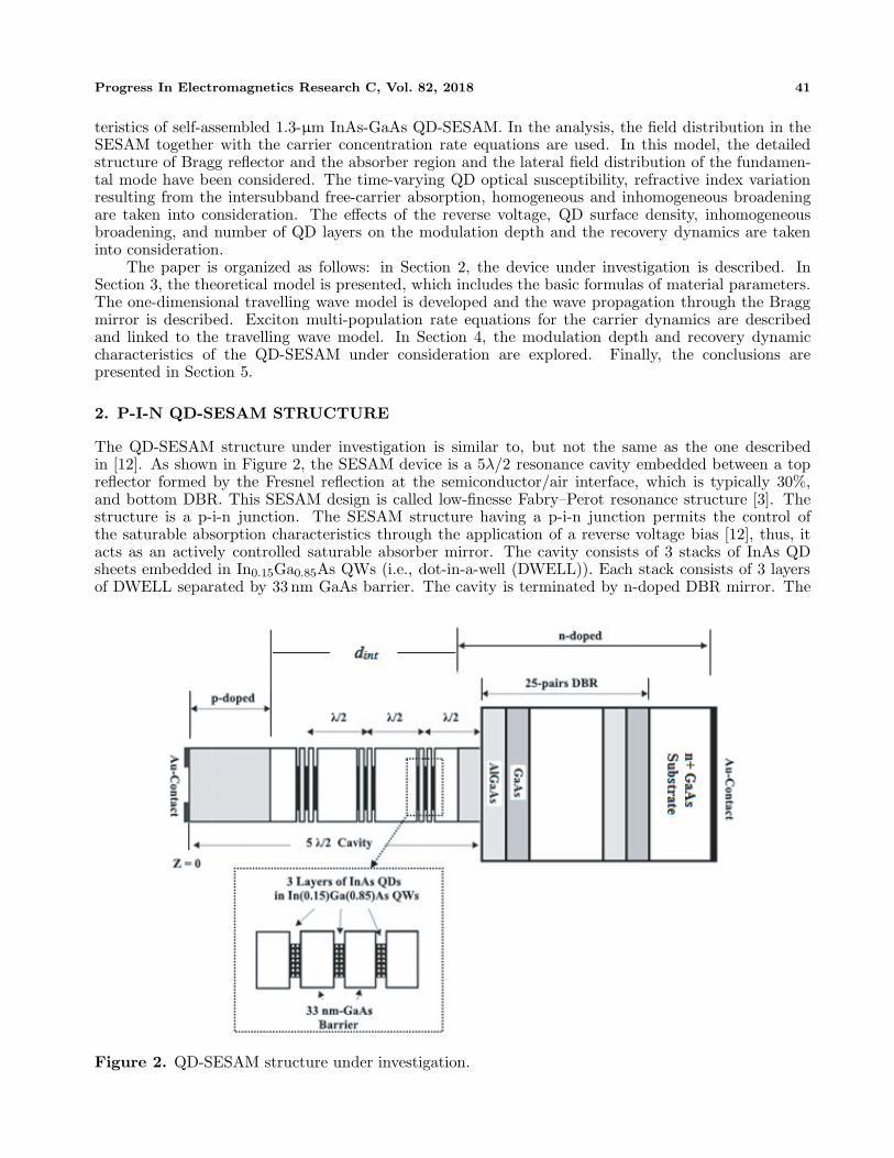
The QD-SESAM structure under investigation is similar to, but not the same as the one describedin [12]. As shown in Figure 2, the SESAM device is a 5λ/2 resonance cavity embedded between a topreflector formed by the Fresnel reflection at the semiconductor/air interface, which is typically 30%,and bottom DBR. This SESAM design is called low-finesse Fabry–Perot resonance structure [3]. Thestructure is a p-i-n junction. The SESAM structure having a p-i-n junction permits the control ofthe saturable absorption characteristics through the application of a reverse voltage bias [12], thus, itacts as an actively controlled saturable absorber mirror. The cavity consists of 3 stacks of InAs QDsheets embedded in In0.15Ga0.85As QWs (i.e., dot-in-a-well (DWELL)). Each stack consists of 3 layersof DWELL separated by 33 nm GaAs barrier. The cavity is terminated by n-doped DBR mirror. The
Figure 2. QD-SESAM structure under investigation.

42 AbouElEz et al.
DBR mirror consists of 25 pairs of GaAs/Al0.9Ga0.1As. Al0.9Ga0.1As has a lower refractive index, whileGaAs has a higher refractive index. The 25 pairs are terminated by a half pair of the lower refractiveindex, which is not shown in Figure 2. The first layer of the DBR seen from the inner cavity is assumedto be manufactured from Al0.98Ga0.02As, which is used to create 20-nm AlO3 native oxide apertureof diameter equal to the SESAM aperture. The SESAM aperture radius is assumed to be 80 µm.The purpose of oxide aperture is to make a kind of wave index-guiding. AlO3 is assumed to have arefractive index of 1.5296. Due to the presence of the oxide layer, the field is confined radially, andthe device has a step index-guided structure in the radial direction between the core, of the aperturediameter, and the cladding [13]. Core refractive index is the refractive index of the layer material,while cladding refractive index is lower than that of the core because of the presence of the oxide layerwith low refractive index. Finally, the absorption loss coefficient in each layer of the device is assumedto be as follows [14]; 1.6457 cm−1, 1.1861 cm−1 for (n-Al0.9Ga0.1As/n-GaAs), respectively. 0.85 cm−1,3.0428 cm−1 for (p-Al0.9Ga0.1As/p-GaAs), respectively. For i-GaAs barrier, the loss is assumed to be5 cm−1.
3. THEORETICAL MODEL
The theoretical model constitutes two parts; the travelling wave equations describing the dynamic fieldvariation along the device and the rate equations that describe the carrier dynamics. In order to studythe reflectivity and the recovery dynamics of the SESAM, these parameters are studied with an incidentpulse on the SESAM with an applied reverse voltage.
3.1. Travelling Wave Equations
At fixed wavelength (i.e., operating wavelength at λo = 1.3 µm) and assuming the lateral distributionof the field to be the fundamental linearly polarized LP01 mode [15, 16], the electric field along theproposed laser structure in z-direction as a function of time t can be represented as a superpositionof two slowly varying envelopes, AF (z,t) and AB(z,t), of the forward and backward propagating wavesof the carrier frequency. The slowly varying envelope of the electric field can be shown to satisfy thefollowing travelling wave equation in the longitudinal z direction for each of the forward and backwardtraveling waves [9–11];
±∂AF/B (z, t)∂z
+(neff
c
) ∂AF/B (z, t)∂t
= −αi
2AF/B (z, t)−j ωo
cΔnF−effA
F/B (z, t)−(j
12ωo
cneff
)P
F/Beff (z,t) (1)
In non-active regions, the last two terms do not contribute. neff is the mode effective refractiveindex in each dielectric layer in the structure, where mode propagation constant βo = koneff , and ko isthe free space propagation constant [15, 16]. c is the speed of light. The effective refractive index of themode can be calculated in terms of the difference between the core and the cladding refractive indices.Core refractive index is the refractive index of the layer material, while cladding refractive index is lowerthan that of the core because of the presence of the oxide layer with low refractive index. The effectivedifference between core and cladding refractive indices is calculated according to the method describedin [13] which has a value of 0.0168. The fundamental mode effective refractive indices in the differentmaterials are calculated to be 3.4109, 2.9514, 3.4504, and 3.4128 for GaAs, Al0.9Ga0.1As, DWELLLayer, and Cavity (i.e., GaAs barrier & DWELLs), respectively. αi is the internal loss coefficient ineach layer, ωo the angular frequency corresponding to operating wavelength λo, ΔnF−eff the refractiveindex variations which result from the intersubband free-carrier absorption (FCA), and PF/B(z,t) theslowly varying effective (forward/backward) dynamic polarization term of the active region.
In the follows, the different factors affecting the travelling wave equations are described.
3.1.1. Treatment of Inhomogeneous Broadening
The calculation of the last two terms in Eq. (1) is based on the assumption that QDs exhibit size andcomposition fluctuations, producing an inhomogeneous broadening of energies for the confined states of
Progress In Electromagnetics Research C, Vol. 82, 2018 43
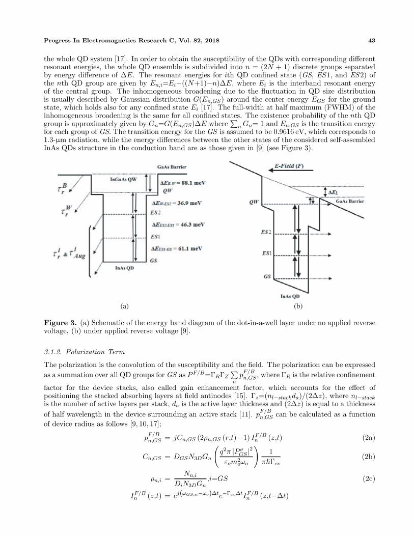
the whole QD system [17]. In order to obtain the susceptibility of the QDs with corresponding differentresonant energies, the whole QD ensemble is subdivided into n = (2N + 1) discrete groups separatedby energy difference of ΔE. The resonant energies for ith QD confined state (GS, ES1, and ES2) ofthe nth QD group are given by En,i=Ei−((N+1)−n)ΔE, where Ei is the interband resonant energyof the central group. The inhomogeneous broadening due to the fluctuation in QD size distributionis usually described by Gaussian distribution G(En,GS) around the center energy EGS for the groundstate, which holds also for any confined state Ei [17]. The full-width at half maximum (FWHM) of theinhomogeneous broadening is the same for all confined states. The existence probability of the nth QDgroup is approximately given by Gn=G(En,GS)ΔE where
∑nGn= 1 and En,GS is the transition energy
for each group of GS. The transition energy for the GS is assumed to be 0.9616 eV, which corresponds to1.3-µm radiation, while the energy differences between the other states of the considered self-assembledInAs QDs structure in the conduction band are as those given in [9] (see Figure 3).
(a) (b)
Figure 3. (a) Schematic of the energy band diagram of the dot-in-a-well layer under no applied reversevoltage, (b) under applied reverse voltage [9].
3.1.2. Polarization Term
The polarization is the convolution of the susceptibility and the field. The polarization can be expressedas a summation over all QD groups for GS as PF/B=ΓRΓZ
∑np
F/Bn,GS , where ΓR is the relative confinement
factor for the device stacks, also called gain enhancement factor, which accounts for the effect ofpositioning the stacked absorbing layers at field antinodes [15]. Γz=(nl−stackda)/(2Δz), where nl−stack
is the number of active layers per stack, da is the active layer thickness and (2Δz) is equal to a thicknessof half wavelength in the device surrounding an active stack [11]. pF/B
n,GS can be calculated as a functionof device radius as follows [9, 10, 17];
pF/Bn,GS = jCn,GS (2ρn,GS (r,t)−1) IF/B
n (z,t) (2a)
Cn,GS = DGSN3DGn
(q2π |P σ
GS |2εom2
oωo
)1
π�Γcv(2b)
ρn,i =Nn,i
DiN3DGn,i=GS (2c)
IF/Bn (z,t) = ej(ωGS,n−ωo)Δte−ΓcvΔtIF/B
n (z,t−Δt)

44 AbouElEz et al.
+ΓcvΔt
2
[AF/B (z,t) +AF/B (z,t) ej(ωGS,n−ωo)Δte−ΓcvΔt
](2d)
where, Cn,GS is a constant factor, ρn,i the occupation probability of the nth QDs group and ith energylevels, Nn,i the carrier density in the ith QD confined state of the nth QD group, and Di the degeneracyof the ith QD energy level assumed to be 2, 4, 6 for GS, ES1, and ES2, respectively [9]. The carrierdensity will be obtained by the solution of the rate equations as will be described in the electrical model.In Eq. (2b), (N3DGn) gives the QD volume density in the nth QD group, where N3D=Nsd/hQD is theQD volume density, Nsd the QD surface density per layer, and hQD the average QD height. Along withthis, q and εo are the electron charge and permittivity of free space, respectively. |P σ
GS |2 is the momentummatrix element [17]. The momentum matrix element |P σ
GS |2 is calculated equal to 2.9848×10⁻³⁰ kg eV.In Eq. (2b), 1/Γcv represents the characteristic dephasing time of the interband transition which isrelated to FWHM of the homogeneous broadening by Fhom= 2�Γcv. The FWHM of the homogeneousbroadening is assumed to be 18 meV at 300 K. IF/B
n (z,t) in Eq. (2a) represents the convolution integralbetween the complex Lorentzian function in the time domain and (forward/backward) slowly varyingfield amplitude, which represents time domain filtering of the field by the Lorentzian function [9]. ωGS,n
is the radial frequency corresponding to the interband resonant energy of group n ofGS.
3.1.3. Free Carrier Absorption Term
The field equations are affected also by the refractive index variations which result from the intersubbandfree-carrier absorption (FCA), calculated as a function of time and device radius at ωo according to therelation given in [11, 18];
ΔnF (r,t,ωo) = − q2
2neff εoω2o
⎡⎣Γz
⎛⎝NW (r,t)
m∗eW
+∑n,i
Nn,i (r,t)m∗
eD
⎞⎠+ΓB
NB (r,t)m∗
eB
⎤⎦ (3)
where NB and NW are the carrier densities in the barrier and QW, respectively. m∗eD, m∗
eW , and m∗eB are
the electron effective masses of QD, QW, barrier materials, respectively. The electron effective massesof the GaAs barrier, In0.15Ga0.85As QW, and InAs QD are (0.0665)mo, (0.06)mo, and (0.023)mo [19],respectively.
3.1.4. Effective Parameters and Gain Suppression Coefficient
For any radially dependent parameter X, such as optical susceptibility or refractive index change due tothe intersubband transitions, an effective value of the parameter is used in the z-directional travellingwave equation, which is weighted by the lateral distribution of the field through the following relationXeff =
∫∞0 X(r)|ψN (r)|2rdr [7]. The normalized fundamental transverse mode distribution |ψN (r)|2 has
a dimension of [1/m2] [11].To take into account the nonlinear absorption suppression, the polarization term given by Eq. (2a) is
further multiplied by a factor of the form 1/(1+εcS(r,t)), where εc [m3] is the nonlinear gain coefficient,which is a function of FWHM of the homogeneous broadening and the photon lifetime [17]. Thenonlinear gain coefficient is calculated to be 1.0603 × 10⁻²⁴ m3 at T = 300 K [17]. S(r,t) is the photondensity inside the cavity which can be calculated simply from the energy density of the electric fieldthrough the following relation [11, 20];
S (r,t) =
(εon
2eff
2�ωo
)[∣∣AF (z,t)∣∣2 +
∣∣AB (z,t)∣∣2] |ψN (r)|2 (4)
As will be described in the electrical model section, Eq. (4) can be considered as a link betweenthe travelling waves amplitudes and stimulated emission term in the rate equations.
3.2. Numerical Solution of the TDTW Equations and the Boundary Conditions
The distribution of AF/B(z,t) along the absorber cavity and the DBRs can be represented in thenumerical implementation at k + 1 interfaces at the boundaries of dielectric layers, where k is the total

Progress In Electromagnetics Research C, Vol. 82, 2018 45
number of dielectric layers. The thickness of the ith dielectric layer is assumed equal to Δzi, where iis an integer, and the position of the boundary between the ith and (i − 1)th layers is zi. Dielectriclayer thickness Δzi is varied according to its effective refractive index such that the layer length delta zis equal to a quarter wavelength (λo/(4neff (i))) which is a necessary condition for the operation of theDBR. A suitable choice for the relation between time and spatial steps in the z direction in the solutionof Eq. (1) is Δt = (Δzineff (i)/c), and Δt will be a constant time step. In the simulation, the travelingwaves, AF/B(z,t), are advanced from one dielectric interface at time t to the next interface at t + Δt.Across active layers, where the QD stacks are placed, Eq. (1) can be solved with the first-order finitedifference approximation, as follows [11];
AF (zi+Δzi,t+Δt) = AF (zi,t) +(−αi
2−jkoΔnF−eff (t)
)AF (zi,t) Δzi−jPF
eff (zi,t) Δzi (5a)
AB (zi,t+Δt) = AB (zi+1,t) +(−αi
2−jkoΔnF−eff (t)
)AB (zi+1,t) Δzi−jPB
eff (zi+1,t) Δzi (5b)
At the interfaces between two layers, boundary conditions are applied. At each time step, theboundary conditions for reflection and transmission are applied to the propagating fields at the dielectricinterfaces by using Eq. (6). The amplitudes of propagated fields, AF/B
out in terms of the incident fieldsand A
F/Bin at the boundary between the dielectric layers, can be determined using the transfer matrix
as follows [11, 16]; [AF
out
ABout
]=[t11 r12r21 t22
] [AF
ine−jϕ
ABine
−jϕ
](6)
where the corresponding transmission coefficients are t11=2neff (i−1)/(neff (i)+neff (i−1)); and thecorresponding reflection coefficients are r12= −r21=(neff (i)−neff (i−1))/(neff (i)+neff (i−1)); neff (i−1)are the effective refractive indices of the mode in adjacent ith and (i − 1)th layers, respectively. Asstated in the previous section, AF (z,t) and AB(z,t) slowly vary with respect to both z and t; however,the operation of the DBR requires that the length of each of its layers must be quarter wavelength.Thus, a phase shift of ϕ = (π/2) across the layer is included in Eq. (6). Thus the amplitudes (i.e.,AF (z,t) and AB(z,t)) slowly vary with respect to time, whereas they include the phase variation withz as described. The boundary conditions at the top and bottom surfaces of the Bragg reflectors can bewritten as;
AB (t, zk+1) = rRAFin (t, zk+1)
AF (t, z1) = ABin (t, z1) rL +
√(1 − r2L
) (Pin (t)
√μo/εo
) (7)
The reflectivity and recovery dynamics of the SESAM are studied for an incident pulse, thus theinstantaneous pulse power incident on the SESAM aperture Pin(t) is introduced in the boundarycondition at the sesam-air interface. The pulse has temporal Gaussian shape with defined energyEp and FWHM duration time τp, assuming an incident optical pulse transverse distribution matchingthe LP01 transverse distribution in the device. In Eq. (7), rL is semiconductor-air reflectivity at z = 0.The semiconductor-air reflectivity rL = 0.55 and semiconductor-metal reflectivity rR = −0.974. Theoutput power is calculated according to the following equation [11, 20];
Pout≈ c�ωo
(εo
2�ωo
) ∣∣ABout(z1)
∣∣2 (8)
3.3. Electrical Model and Rate Equations of Carrier Density in the Saturable Absorber
In this section the electrical model will be presented. Figure 3(a) shows energy band diagram for thedot-in-a-well layer under no applied reverse voltage, and Figure 3(b) shows its deformation under appliedreverse voltage [9]. Numerical values of energy differences between confined states for the QD groupwith the highest existence probability are indicated. The deformation leads to enhanced tunneling andthermionic escape rates.

46 AbouElEz et al.
3.3.1. Effects of Revers Voltage
The applied reverse voltage causes the formation of a triangular barrier as shown in Figure 3(b). Dueto the applied reverse voltage, the barrier height energy is lowered by ΔEL = hQD·q · F/2 [4] wherehQD is the QD height and F the electric field caused by reverse biase voltage which is perpendicularto the p-i-n junction. This electric field is calculated as F = (Vr + Vbi)/dint, where Vr is the appliedreverse voltage, Vbi the built-in potential assumed to be 0.8 V [4], and dint the intrinsic region length inthe cavity.
The main effects influencing the carrier dynamics under an applied reverse voltage are enhancedthermionic escape rates from the QD ES2 to the QW and from QW to barrier state which are due toa linear barrier reduction induced by the applied voltage. For high applied reverse voltage, the widthof this barrier may decrease sufficiently to allow carriers to tunnel from the GS, ES1, and ES2 and theQW directly to the 3-D states in the barrier, shown by horizontal arrows in Figure 3(b).
A weak quantum confinement Stark effect (QCSE) in QD structures has also been observedcompared with QW structures [4]. For simplicity, this weak QCSE will be neglected in our model,whereas the influence of the applied field on both thermionic and tunneling escape processes will beproperly introduced using simple approaches.
Expressions for the tunneling escape rates from the QD confined k states (i.e., k refers to the nthgroup of each ith confined state GS, ES1, and ES2) and from the QW to the 3-D states in the barriercan be expressed for a triangular well as follows [4];
Rtun k = ftun exp
(−4
3
√2m∗
eB (ΔEB−k)3/2
q�F
)(9a)
Rtun W = ftun exp
(−4
3
√2m∗
eB (ΔEB−W )3/2
q�F
)(9b)
The tunneling rates given by Eqs. (9a)–(9b) are calculated by multiplying the barrier collisionfrequency ftun = �π/2m∗h2
QD of the carriers in QD/QW with the barrier transmission probability(the exponential term), which is estimated by Wentzel-Kramer-Brillouin approximation [4]. m∗
eB is theelectron effective mass of GaAs barrier, and m∗ is the electron effective mass of QD/QW material [9].The reverse voltage affects also enhances thermionic escape rates as will be indicated later.
3.3.2. Carriers Rate Equations
The rate equations describe the carrier density dynamics in different energy levels. Carriers are generatedin the confined GS level by the pulse injection with photon energy tuned to the GS transition of the QD.The generated carriers are then transferred between the energy states by relaxation, capture, escape,and tunneling, and then disappear by current drift from the barrier and by carrier recombination.
The dynamics of carrier density as a function of the radius in the device are presented in a set ofrate equations. The first rate Eq. (10a) is for carrier density NB in the 3-D barrier state. The secondrate Eq. (10b) describes carrier density NW in the 2-D QW state Finally. There are n rate Eqs. (10c)–(10e) for the carriers (electrons for exciton model) density Nn,i in the ith QD state of the nth QD groupas follows [9];
dNB (r,t)dt
= −μBNBV + Vbi
d2int
+NW
τW−B−(
1τB−W
(1−ρW ) +1τBr
)NB
+Rtun WNW +
∑k
Rtun kNk (10a)
dNW (r,t)dt
=NB
τB−W(1−ρW ) +
∑n
Nn,ES2
τn,ES2−W− NW
τW−ES2
∑n
(1−ρn·ES2)Gn
− NW
τW−B− 1τWr
−Rtun WNW (10b)

Progress In Electromagnetics Research C, Vol. 82, 2018 47
dNn,ES2 (r,t)dt
=NWGn (1−ρn,ES2)
τW−ES2+
Nn,ES1
τES1−ES2(1−ρn·ES2)− Nn,ES2
τES2−ES1(1−ρn,ES1)
− Nn,ES2
τES2−W(1−ρW )−Nn,ES2ρn,ES2
τES2Aug
−Nn,ES2
τES2r
−Rtun n,ES2Nn,ES2 (10c)
dNn,ES1 (r,t)dt
=Nn,ES2
τES2−ES1(1−ρn,ES1) +
Nn,GS
τGS−ES1(1−ρn,ES1)− Nn,ES1
τES1−GS(1−ρn,GS)
− Nn,ES1
τES1−ES2(1−ρn,ES2)−Nn,ES1ρn,ES1
τES1Aug
−Nn,ES1
τES1r
−Rtun n,ES1Nn,ES1 (10d)
dNn,GS (r,t)dt
=Nn,ES1
τES1−GS(1−ρn,GS)− Nn,GS
τGS−ES1(1−ρn,ES1)
−Nn,ES1ρn,ES1
τGSAug
−Nn,ES1
τGSr
−Rtunn,GSNn,GS+Rgeneration,n (10e)
The first term in Eq. (10a) accounts for the electron drift current from the barrier to the biascircuit under applied reverse voltage. μB is the electron mobility of the GaAs barrier material whichis given by μB = 7200(300/T )2.1 cm2/V · s [19]. ρW is the occupation probability in the QW state [19].Rtun k and Rtun W are the tunnelling rates from the QD states and QW to the barrier which are givenby Eqs. (9a) and (9b), respectively. τB−W is the carrier capture time to the QW and is assumed to be0.3 ps [9, 21]. The enhanced thermionic escape time from the QW to the barrier state can be modelledas follows [9];
τW−B (V ) =(τB−W
DOSWhWnl
DOSBdintexp
(ΔEB−W
kBT
))exp
(−ΔEL (V )
kBT
)(11a)
where DOSB is the effective density of states per unit volume in the GaAs barrier [11]. DOSW is theeffective density of states per unit volume in the QW layer [11]. dint is the intrinsic region length asshown in Figure 2. τB
r and τWr are the carrier recombination times in GaAs barrier and InGaAs QW,
respectively. Their values are assumed to be 400 ps [21]. In Eq. (10b), τW−ES2 is the average relaxationtime from QW to ES2 while τn,ES2−W is the enhanced thermionic escape time from ES2 to QW foreach QD group, given by [9];
τn,ES2−W (V ) =(τW−ES2
DES2N3D
DOSWexp
(ΔE(W−n,ES2)
kBT
))exp
(−ΔEL (V )
kBT
)(11b)
ΔE(W−n,ES2) is the energy difference between QW band edge and ES2 energy levels of the n QD groupsin the conduction band. DES2 is the degeneracy of ES2.
The carrier density Nn,i in the ith QD state of the nth QD group is related to the correspondingoccupation probability via Eq. (2c). The carrier lifetime in GS, ES1, and ES2 are denoted by τGS
r , τES1r
and τES2r , respectively. The carrier lifetime for all QD states is assumed equal to 1 ns [19]. The
characteristic Auger recombination times, τ iAug with i = GS, ES1, ES2 of QD confined states, are
assumed to have values of 660, 270, and 110 ps, respectively [9, 21].It is assumed that relaxation and capture times between energy levels exist only between adjacent
states. Carriers relaxation time from QW to ES2 is expressed as τW−ES2 = 1/(Ac + CcNW ) which isassumed to be identical for all groups [22]. The average intradot relaxation times from the QD ith tojth level with subscripts i, j = GS, ES1, ES2 can be expressed, with the hypothesis that the final stateis empty, as τi−j(i �= j) = 1/(Ao +CoNW ) [19, 22]. Ac and Ao are the phonon-assisted relaxation rates,while Cc and Co are the Auger relaxation rates. The values of Ac and Cc are assumed to be 1×10¹² s−1
and 1×10⁻¹⁴ m3 s−1, respectively. Ao and Co are assumed to be 5×10¹¹ s−1 and 3.5×10⁻¹³ m3 s−1,respectively [22].
Furthermore, there is an exponential relationship between the relaxation times and escape scapetimes in QD confined states. The escape times from confined state i to confined state j can be obtainedin terms of relaxation times from confined stat j to confined state i as follows [9, 19];
τ(i−j) =(τ(j−i)
Di
Djexp
(ΔEi−j
kBT
))(12)

48 AbouElEz et al.
where ΔEi−j is the interband energy difference between two successive levels. The carrier generationrate term in Eq. (10e) is given by;
Rgeneration,n = ΓR
(c
neff
)[ωo
cneffCGS,n (1 − 2ρn,GS (r,t))
11+εcS (r,t)
]
×(εon
2eff
2�ωo
[R(AF∗ (z,t) IF
n (z,t))
+R(AB∗ (z,t) IB
n (z,t))] |ψN (r)|2
)(13)
where R denotes the real part, and the second bracket in the right-hand side represents the absorptionwhile the last bracket includes the photon density of the forward and backward fields together with theLorentzian function filtering.
4. SIMULATION RESULTS AND DISCUSSION
In this section, we will first examine the modulation depth ΔR as a function of different operatingparameters such as reverse bias voltage, QD surface density, number of QD absorbing layers, and FWHMof inhomogeneous broadening for the device under consideration described above. The absorptionrecovery dynamics are then studied considering the effects of the above parameters. The number of QDgroups is taken to be 9, and the FWHM of the homogeneous broadening is assumed to be 18 meV at300 K for all studied cases.
4.1. Modulation Depth ΔR
Gaussian pulses with 130 fs width and energy fluences in the range 0.01–1000 µJ/cm2 are incident on theQD-SESAM. The photon energy of each pulse is tuned to the ground state transition of the QD (i.e.,0.9616 eV). Figure 4(a) shows the reflectivity as a function of pulse energy fluence with different valuesof applied reverse voltage and a constant value of inhomogeneous broadening of 40 meV. It is noted thatthe modulation depth ΔR is not affected by the applied reverse voltage. The calculated modulationdepth is nearly equal to 3.12% and the saturation fluence Fsat ≈ 0.84 µJ/cm2 and non-saturable lossΔRns ≈ 0.25%. This result is interpreted by the fact that the applied reverse voltage affects the escape
(a) (b)
(c) (d)
Figure 4. SESAM reflectivity versus incident pulse fluence at (a) different applied reverse voltages,(b) different values of QD surface density, (c) different values of inhomogeneous broadening, and (d)different values of the number of QD absorbing layers in the cavity.

Progress In Electromagnetics Research C, Vol. 82, 2018 49
times and accordingly the transient recovery, but does not affect the reflectivity at steady state. Also,the applied reverse voltage results in weak QCSE in QD compared to its effect in QW based SESAMdevices. This result is consistent with that obtained experimentally in [5]. The main differences betweenthe result shown in Figure 4(a) under the assumption of LP01 lateral distribution of the field and theresult shown in Figure 1 for flat-top distribution of the field are in the value of ΔRns which is muchsmaller for the LP01 case, and in the value of Fsat which is approximately half the value of the flat-topcase [2]. The smaller value of ΔRns may be interpreted to be due to the confined field for the LP01
distribution which leads to lower losses.One of the methods used to control the modulation depth in QD-SESAM devices is controlling the
QD surface density. To examine the effect of QD surface density on the modulation depth, differentvalues of QD surface density of 3×1010 cm−2, 4×1010 cm−2, and 5×1010 cm−2 are assumed with constantapplied reverse voltage of 3 V and inhomogeneous broadening of 40 meV. As shown in Figure 4(b), asthe QD surface density increases the modulation depth increases. Table 1 gives Rlin, ΔR and Fsat
corresponding to each QD surface density value. This result is, qualitatively, in agreement with theexperimental work which showed that the modulation depth is proportional to the QD surface density [6].This result can be explained as follows. The value of the reflectivity of a saturated SESAM Rns isconstant for all QD surface densities. On the other hand, Rlin decreases with increasing the absorption,which is proportional to the susceptibility (see Eq. (2)), thus by increasing QD surface density, theabsorption increases, reflectivity decreases, and accordingly ΔR increases.
Table 1. QD-SESAM parameters at different QD surface density.
Nsd Rlin ΔR Fsat
5 × 1010 cm−2 96.607% 3.12% 0.84 µJ/cm2
4 × 1010 cm−2 97.225% 2.5% 0.84 µJ/cm2
3 × 1010 cm−2 97.846 % 1.88% 0.84 µJ/cm2
Other device parameters can also lead to increasing the modulation depth. As stated above inconnection with Eq. (2), the absorption can be increased by increasing the value of pF/B
n,GS of the QD grouprelated to the operating wavelength (i.e., center group) by decreasing the FWHM of inhomogeneousbroadening. Increasing the number of QD layers leads to a similar result. This can be interpreted asfollows. It can be seen from the expression of PF/B (preceding Eq. (2a)) that the change of the numberof layers affects the values of ΓR and ΓZ , where the effect of ΓZ is more dominant, i.e., as the numberof layers increases the effective polarization PF/B in Eq. (2a) increases, which increases the absorption.
The effect of inhomogeneous broadening on the modulation depth is examined for different valuesof Fihom of 40, 30, 20 meV at constant applied reverse voltage of 3 V and constant surface density of5 × 1010 cm−2. Figure 4(c) illustrates this effect. It is clear that the linear reflectivity increases withincreasing Fihom, and accordingly the modulation depth decreases. Table 2 gives Rlin, ΔR and Fsat
which correspond to each value of inhomogeneous broadening.
Table 2. QD-SESAM parameters at different FWHM values of the inhomogeneous broadening.
Fihom Rlin ΔR Fsat
40 meV 96.607% 3.12% 0.84 µJ/cm2
30 meV 96.200% 3.53% 0.86 µJ/cm2
20 meV 95.566% 4.16% 0.81 µJ/cm2
Finally, the effect of changing the number of QD absorbing layers in the cavity on the modulationdepth is investigated. The number of layers considered in the cavity is taken to be 3, 6, and 9 (i.e., thenumber of layers per stack is 1, 2, and 3, respectively). The value of inhomogeneous broadening andvalue of the applied reverse voltage are assumed to be 40 meV and 3 V, respectively. Figure 4(d) shows

50 AbouElEz et al.
Table 3. QD-SESAM parameters at different values of the number of layers.
Nlayers Rlin ΔR Fsat
3 98.515% 1.22% 0.72 µJ/cm2
6 97.409% 2.32% 0.76 µJ/cm2
9 96.607% 3.12% 0.84 µJ/cm2
that increasing the number of layers increases the value of the modulation depth, as mentioned above.Table 3 gives Rlin, ΔR and Fsat for different numbers of QD absorbing layers in the cavity.
4.2. Absorption Dynamics
The absorption recovery dynamics in the experimental work is normally investigated using the pump-probe technique. In this technique, a high intensity short pulse with fluence above Fsat is injected tothe SESAM [4, 5]. The recovery dynamics of the SESAM is monitored by injecting weak probe pulseswith variable delay times relative to the pump pulse and monitoring the reflection from the SESAM forthese delayed probe pulses. The probe pulse energy in this technique is assumed to be small enoughsuch that the absorption dynamics is not significantly perturbed.
The absorption recovery dynamics using the pump-probe technique is modeled in this section. Thepump pulse and probe pulse are assumed to have Gaussian shape and 130 fs width. The pump pulse hasa fluence of 10 µJ/cm2, which is greater than the saturation fluences calculated in the previous section.The probe pulses have a fluence of 0.01 µJ/cm2. The probe pulses are considered to have the samefrequency of the pump pulse which is resonant with the GS transition energy. The absorption of thepump pulse with high energy fluence causes the generation of carriers in the QD GS groups, leading toa significant absorption bleaching. The dynamics of reflectivity changes of the probe pulse induced bythe pump pulse at different delay time intervals τ are calculated as dR(τ) = R(τ)−Ro where Ro is thereflectivity for probe pulses under no applied pump pulse.
At first, the recovery dynamics of the reflectivity change will be examined considering the effectof the applied reverse voltage, as shown in Figure 5(a). The response can be fitted well with three
(a) (b)
(c) (d)
Figure 5. (a) The recovery dynamics of the reflectivity change for different values of applied reversevoltage ranging from 0–5 volt. The recovery dynamics of the normalized reflectivity change at differentreverse voltage (0, 3, and 5 volt) for (b) different values of QD surface density, (c) different values ofQD inhomogeneous broadening, and (d) different values of QD absorbing layers in the cavity.

Progress In Electromagnetics Research C, Vol. 82, 2018 51
components with different time constants according to the following equation;
dRfitted (τ) = A exp (−τ/τ1) +B exp (−τ/τ2) + C exp (−τ/τ3) (14)
where τ1 corresponds to the fast component time constant,and A is its amplitude. The slow recoveryhas two stages with slow time constants τ2 and τ3, respectively. B and C are the amplitudes of thesecomponents. Table 4 shows the values of the three time constants for different applied reverse voltages.
Table 4. Fitting time constants for different applied reverse voltages.
Applied Voltage 0 1 2 3 4 5τ1 (ps) 2.73 2.56 2.42 2.22 2.08 1.93τ2 (ps) 53.28 49.46 42.48 31.51 22.37 15.27τ3 (ps) 223.0 156.78 121.16 87.67 67.48 50.50
As shown in Figure 5(a) and Table 4, the fast recovery time constant τ1 changes from 2.73 to1.93 ps as the applied reverse voltage changes from zero to 5 volt. This time constant is related to theexcitation of the photo-generated carriers from GS to higher energy states ES1 and ES2 [9]. It is clearthat the absorption recovery dynamics are dominated by the slow time constants τ2 and τ3 which arehighly dependent on the applied voltage. As expected, as the reverse applied voltage increases the slowrecovery time constants τ2 and τ3 decrease. This result can be explained in view of Eq. (9) and Eq. (11)for the thermionic and tunneling processes. As the applied reverse voltage increases, the electric fieldF across the QD layers increases which in turn enhances the thermal escaping rate and tunneling rateleading to faster recovery time. The absorption recovery is finally completed as a result of nonradiativerecombination and spontaneous emission processes occurring on a time scale of hundreds of picoseconds.The obtained results are consistent with the behavior of the experimental results given in [4–6].
Now, the effect of QD surface density on recovery dynamics will be investigated. Different valuesof QD surface density of 3 × 1010 cm−2, 4 × 1010 cm−2, and 5 × 1010 cm−2 are assumed. Results areobtained for applied reverse voltage of zero (i.e., the effect of reverse applied voltage is neglected), 3,and 5 volt. The inhomogeneous broadening of 40 meV and the number of QD layers of 9 are constant.Figure 5(b) shows the reflectivity change normalized with respect to its peak value for these assumedconditions. At zero voltage, the effect of QD surface density on the recovery dynamics is maximum,and this effect decreases with increasing the reverse voltage. Table 5 gives the fitting time constantsfor different values of QD surface density at zero volt. It can be noted from Figure 5(b) and Table 5that the slow recovery time constants increase as the surface density increases. This result does notagree with the experimental result given in [6]. In [6], the measurement shows that by increasing theQD coverage the recombination becomes faster, and this result is explained by a higher defect densitythat leads to a faster recombination or a higher interdot transfer probability caused by the smallerdistances between the dots. In our model, it is assumed that the carrier lifetime for all QD states andthe characteristic Auger recombination times are constant for all assumed QD surface density values.This assumption is considered because of the difficulty of obtaining suitable values for recombinationtimes corresponding to the assumed QD surface density. So, our result, in this case, deviates from thepublished experimental result.
Table 5. Fitting time constants for different values QD surface density at zero volt.
Nsd (cm−2) 3 × 10¹⁰ 4 × 10¹⁰ 5 × 10¹⁰
τ1 (ps) 2.67 2.71 2.73τ2 (ps) 40.56 47.11 53.28τ3 (ps) 168.37 197.40 223.06
Figure 5(c) shows the effect of the inhomogeneous broadening on the recovery dynamics fordifferent values of Fihom of 40, 30, 20 meV at different reverse voltages and constant surface densityof 5× 1010 cm−2. These effects are considered under the assumption that the carrier lifetime for all QDstates and the characteristic Auger recombination times are constant for all values of inhomogeneous

52 AbouElEz et al.
broadening. As can be noted from the data in Table 6, at zero volt there is a slight effect on the recoverydynamics for the three values of the inhomogeneous broadening; as the inhomogeneous broadeningincreases the slow recovery time components increase slightly. At high applied reverse voltage thiseffect vanishes.
Table 6. Fitting time constants for different values QD inhomogeneous broadening at zero volt.
Fihom (meV) 20 30 40τ1 (ps) 2.77 2.76 2.73τ2 (ps) 36.93 45.71 53.28τ3 (ps) 221.03 222.93 223.06
Finally, the effect of changing the number of QD absorbing layers on the recovery dynamics isshown in Figure 5(d) for different values of layers of 9, 6, and 3 and different applied reverse voltages,where the surface density is 5 × 1010 cm−2. Table 7 shows the fitting time constants at zero volt. Atzero volt, the slow recovery time constants increase as the number of QD absorbing layers increases. Athigher applied voltages, this behaviour becomes insignificant. This behaviour can be interpreted as wasdiscussed in connection with the modulation depth, that the increase of the number of QD layers leadsto increase of the polarization. This is similar to the increase of the susceptibility which may result froman increase of the QD volume density (Eqs. (2a)–(2b)). This explains the similarity of the effects of QDsurface density and the number of layers on the recovery dynamics seen in Figure 5(c) and Figure 5(d).
Table 7. Fitting time constants for different values QD absorbing layers in the cavity at zero volt.
Nlayers 3 6 9τ1 (ps) 2.52 2.65 2.73τ2 (ps) 47.91 53.44 53.28τ3 (ps) 141.93 187.02 223.06
5. CONCLUSION
In this paper, a TDTW model is used to analyze the characteristics of a p-i-n QD-SESAM, namelythe modulation depth and the recovery dynamics. The parameters which affect these characteristicsare the reverse applied voltage, QD surface density, QD inhomogeneous broadening, and number ofQD absorbing layers. The results show that the modulation depth of the SESAM is highly affectedby the QD absorbing material parameters. The modulation depth can be increased by increasing theQD surface density, increasing the number of QD absorbing layers, or decreasing the inhomogeneousbroadening of QDs. Also, it is found that the modulation depth is not affected by the reverse appliedvoltage. The recovery dynamics of the QD-SESAM is mainly affected by the applied reverse voltage. Itis found that as the applied reverse voltage increases the slow recovery time constants decrease. Underthe assumption that the carrier lifetime for all QD states and the characteristic Auger recombinationtimes are constant for all above parameters, it is found that the slow recovery time constants increase byincreasing the QD surface density, number of QD absorbing layers, and decreasing the inhomogeneousbroadening. The effect of these parameters becomes insignificant as the applied reverse voltage increases.
REFERENCES
1. Bellancourt, A. R., B. Rudin, D. J. H. C. Maas, M. Golling, H. J. Unold, T. Sudmeyer, and U.Keller, “First demonstration of a Modelocked Integrated External-Cavity Surface Emitting Laser(MIXSEL),” 2007 Conference on Lasers and Electro-Optics (CLEO), 2007.
2. Haiml, M., R. Grange, and U. Keller, “Optical characterization of semiconductor saturableabsorbers,” Applied Physics B: Lasers and Optics, Vol. 79, No. 3, 331–339, 2004.

Progress In Electromagnetics Research C, Vol. 82, 2018 53
3. Keller, U., “Semiconductor nonlinearities for solid-state laser modelocking and Q-switching,” E.Garmire, A. Kost (eds.), Nonlinear Optics in Semiconductors II. Semiconductor and Semimetals,Vol 59, 211–286, Academic Press, San Diego, CA, 1998.
4. Malins, D. B., A. Gomez-Iglesias, S. J. White, W. Sibbett, A. Miller, and E. U. Rafailov, “Ultrafastelectroabsorption dynamics in an InAs quantum dot saturable absorber at 1.3 µm,” Applied PhysicsLetters, Vol. 89, No. 17, 171111, 2006.
5. Zolotovskaya, S. A., M. Butkus, R. Haring, A. Able, W. Kaenders, I. L. Krestnikov, D. A. Livshits,and E. U. Rafailov, “p-i-n junction quantum dot saturable absorber mirror: Electrical control ofultrafast dynamics,” Optics Express, Vol. 20, No. 8, 9038–9045, Mar. 2012.
6. Maas, D. J. H. C., A. R. Bellancourt, M. Hoffmann, B. Rudin, Y. Barbarin, M. Golling, T.Sudmeyer, and U. Keller, “Growth parameter optimization for fast quantum dot SESAMs,” OpticsExpress, Vol. 16, No. 23, 18646–18656, 2008.
7. Yu, S. F., “Dynamic behavior of vertical-cavity surface-emitting lasers,” IEEE Journal of QuantumElectronics, Vol. 32, No. 7, 1168–1179, 1996.
8. Yu, S. F., “An improved time-domain traveling-wave model for vertical-cavity surface-emittinglasers,” IEEE Journal of Quantum Electronics, Vol. 34, No. 10, 1938–1948, 1998.
9. Rossetti, M., P. Bardella, and I. Montrosset, “Time-domain travelling-wave model for quantumdot passively mode-locked lasers,” IEEE Journal of Quantum Electronics, Vol. 47, No. 2, 139–150,2011.
10. Gioannini, M. and M. Rossetti, “Time-domain traveling wave model of quantum dot DFB lasers,”IEEE Journal of Selected Topics in Quantum Electronics, Vol. 17, No. 5, 1318–1326, 2011.
11. Abouelez, A. E., E. Eldiwany, M. B. El Mashade, and H. A. Konber, “Time-domain travelling-wavemodel for quantum dot based vertical cavity laser devices,” Progress In Electromagnetics ResearchM, Vol. 65, 29–42, 2018.
12. Lagatsky, A. A., E. U. Rafailov, W. Sibbett, D. A. Livshits, A. E. Zhukov, and V. M. Ustinov,“Quantum-dot-based saturable absorber with pn junction for mode-locking of solid-state lasers,”IEEE Photonics Technology Letters, Vol. 17, No. 2, 294–296, 2005.
13. Michalzik, R., “Simple understanding of waveguiding in oxidized VCSELs,” Annu. Rep. 1, 19–23,Dept. Optoelectron., Univ. Ulm, Ulm, Germany, 1995.
14. Piskorski, �L., M. Wasiak, R. Sarza�la, and W. Nakwaski, “Structure optimisation of modern GaAs-based InGaAs/GaAs quantum-dot VCSELs for optical fibre communication,” Opto-ElectronicsReview, Vol. 17, No. 3, 217–224, Jan. 2009.
15. Mulet, J. and S. Balle, “Mode-locking dynamics in electrically driven vertical-external-cavitysurface-emitting lasers,” IEEE Journal of Quantum Electronics, Vol. 41, No. 9, 1148–1156, 2005.
16. Yu, S. F., Analysis and Design of Vertical Cavity Surface Emitting Lasers, John Wiley & Sons,2003.
17. Sugawara, M., Self-assembled InGaAs/GaAs Quantum Dots: Semiconductors and Semimetals,Vol. 60, Academic Press, San Diego, CA, 1999.
18. Kim, J., C. Meuer, D. Bimberg, and G. Eisenstein, “Effect of inhomogeneous broadening on gainand phase recovery of quantum-dot semiconductor optical amplifiers,” IEEE Journal of QuantumElectronics, Vol. 46, No. 11, 1670–1680, 2010.
19. Tong, C., S. Yoon, C. Ngo, C. Liu, and W. Loke, “Rate equations for 1.3-µm dots-under-a-well and dots-in-a-well self-assembled InAs-GaAs quantum-dot lasers,” IEEE Journal of QuantumElectronics, Vol. 42, No. 11, 1175–1183, 2006.
20. Agrawal, G. P. and N. K. Dutta, Semiconductor Lasers, 2nd Edition, Van Nostrand, New York,1993.
21. Xu, T., M. Rossetti, P. Bardella, and I. Montrosset, “Simulation and analysis of dynamic regimesinvolving ground and excited state transitions in quantum dot passively mode-locked lasers,” IEEEJournal of Quantum Electronics, Vol. 48, No. 9, 1193–1202, 2012.
22. Berg, T. W. and J. Mørk, “Quantum dot amplifiers with high output power and low noise,” AppliedPhysics Letters, Vol. 82, No. 18, 3083–3085, May 2003.