modeling of cmp - university of california, san...
TRANSCRIPT
© Laboratory for Manufacturing Automation, 2005
University of California at Berkeley
Modeling of CMP
David Dornfeld
CMP researchers: Jihong Choi, Sunghoon Lee, Dr. Hyoungjae Kim, Dr. Dan Echizenya
Department of Mechanical EngineeringUniversity of California Berkeley CA 94720‐1740
http://lma.berkeley.edu
2LMA
© Laboratory for Manufacturing Automation, 2005
University of California at Berkeley
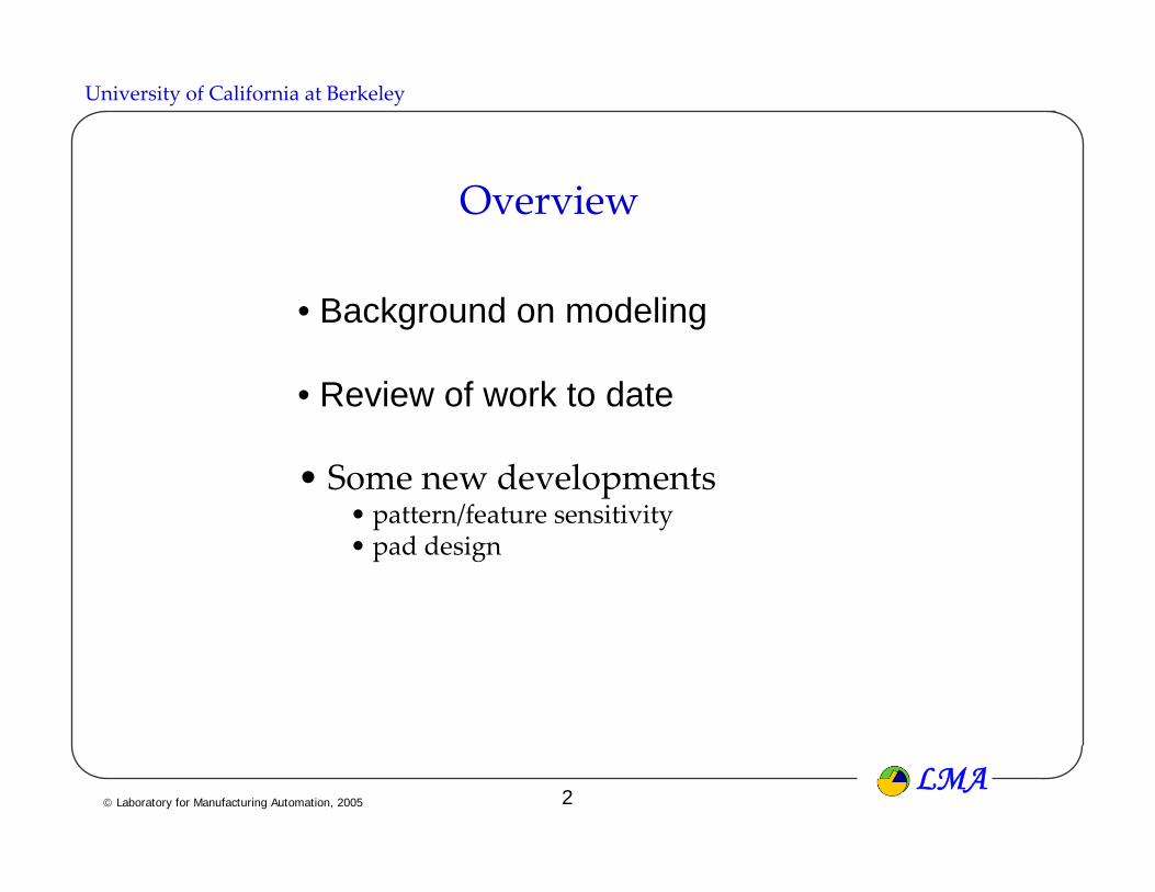
Overview
• Background on modeling
• Review of work to date
• Some new developments• pattern/feature sensitivity• pad design
3LMA
© Laboratory for Manufacturing Automation, 2005
University of California at Berkeley
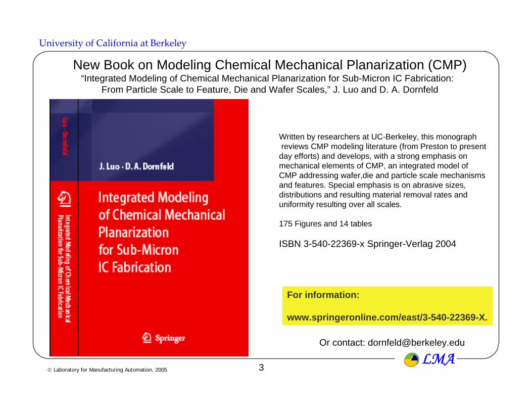
New Book on Modeling Chemical Mechanical Planarization (CMP)“Integrated Modeling of Chemical Mechanical Planarization for Sub-Micron IC Fabrication:
From Particle Scale to Feature, Die and Wafer Scales,” J. Luo and D. A. Dornfeld
For information:
www.springeronline.com/east/3-540-22369-X.
Written by researchers at UC-Berkeley, this monographreviews CMP modeling literature (from Preston to present
day efforts) and develops, with a strong emphasis on mechanical elements of CMP, an integrated model of CMP addressing wafer,die and particle scale mechanisms and features. Special emphasis is on abrasive sizes, distributions and resulting material removal rates and uniformity resulting over all scales.
175 Figures and 14 tables
ISBN 3-540-22369-x Springer-Verlag 2004
Or contact: [email protected]
LMA© Laboratory for Manufacturing Automation, 2005
University of California at Berkeley
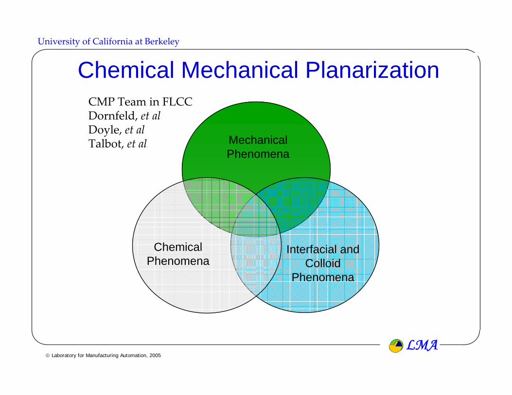
Chemical Mechanical Planarization
Mechanical Phenomena
Chemical Phenomena
Interfacial and Colloid
Phenomena
CMP Team in FLCCDornfeld, et alDoyle, et alTalbot, et al
5LMA
© Laboratory for Manufacturing Automation, 2005
University of California at Berkeley
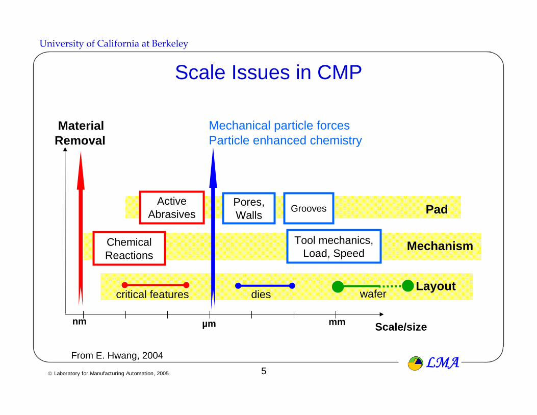
Scale Issues in CMP
From E. Hwang, 2004
Scale/sizenm µm mm
Material Removal
Mechanical particle forcesParticle enhanced chemistry
ChemicalReactions
ActiveAbrasives
Pores,Walls Grooves
Tool mechanics,Load, Speed
critical features dies
Pad
Mechanism
Layoutwafer

6LMA
© Laboratory for Manufacturing Automation, 2005
University of California at Berkeley
w p :pad rotation
tablepad
slurry feedconditioner
head
w w : wafer rotationOscillationF : down force
Backingfilm
Retainerring
Wafer
Wafer Carrier
Pad
Pore Wall
Abrasive particle
CMP Process Schematic
Electro plated diamond conditioner Typical pad
LMA© Laboratory for Manufacturing Automation, 2005
University of California at Berkeley
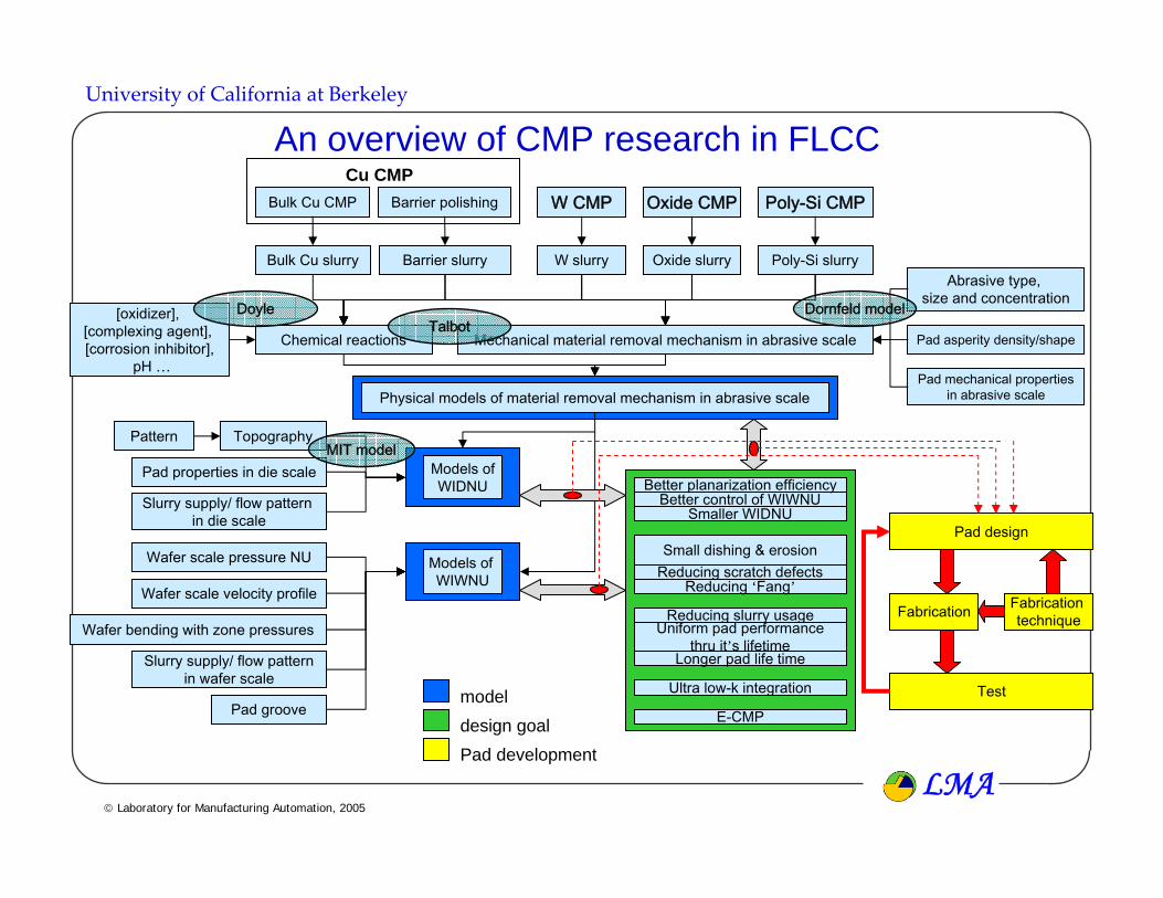
Bulk Cu CMP Barrier polishing W CMP Oxide CMP Poly-Si CMP
Physical models of material removal mechanism in abrasive scale
Chemical reactions
Bulk Cu slurry Barrier slurry W slurry Oxide slurry Poly-Si slurry
Mechanical material removal mechanism in abrasive scale
Abrasive type, size and concentration
[oxidizer], [complexing agent], [corrosion inhibitor],
pH …
Pad asperity density/shape
Pad mechanical propertiesin abrasive scale
Pad properties in die scale
Slurry supply/ flow patternin wafer scale
Wafer scale pressure NU Models of WIWNU
Models ofWIDNU
Topography
Wafer scale velocity profile
Wafer bending with zone pressures
Better control of WIWNU
Reducing ‘Fang’
Small dishing & erosion
Ultra low-k integration
Smaller WIDNU
Reducing slurry usageUniform pad performance
thru it’s lifetimeLonger pad life time
Reducing scratch defects
Better planarization efficiency
E-CMPPad groove
Pad design
Fabrication
Test
Fabrication technique
Slurry supply/ flow pattern in die scale
Cu CMP
modeldesign goalPad development
PatternMIT model
Dornfeld modelDoyle
An overview of CMP research in FLCC
Talbot
8LMA
© Laboratory for Manufacturing Automation, 2005
University of California at Berkeley
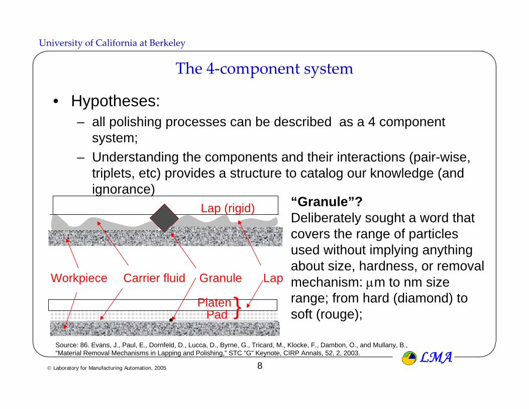
The 4‐component system
• Hypotheses:– all polishing processes can be described as a 4 component
system;– Understanding the components and their interactions (pair-wise,
triplets, etc) provides a structure to catalog our knowledge (and ignorance)
Lap (rigid)
Workpiece LapGranuleCarrier fluid
Platen Pad }
“Granule”?Deliberately sought a word that covers the range of particles used without implying anything about size, hardness, or removal mechanism: µm to nm size range; from hard (diamond) to soft (rouge);
Source: 86. Evans, J., Paul, E., Dornfeld, D., Lucca, D., Byrne, G., Tricard, M., Klocke, F., Dambon, O., and Mullany, B.,“Material Removal Mechanisms in Lapping and Polishing,” STC “G” Keynote, CIRP Annals, 52, 2, 2003.

9LMA
© Laboratory for Manufacturing Automation, 2005
University of California at Berkeley
Six possible pair-wise interactions
• Fluid-workpiece• Workpiece-pad• Workpiece-granule• Granule-pad• pad-fluid• Fluid-granule
10LMA
© Laboratory for Manufacturing Automation, 2005
University of California at Berkeley
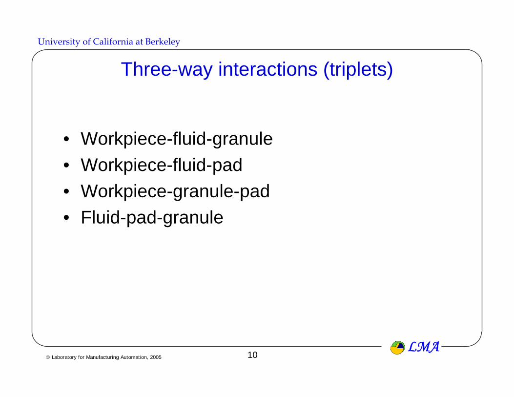
Three-way interactions (triplets)
• Workpiece-fluid-granule• Workpiece-fluid-pad• Workpiece-granule-pad• Fluid-pad-granule
11LMA
© Laboratory for Manufacturing Automation, 2005
University of California at Berkeley
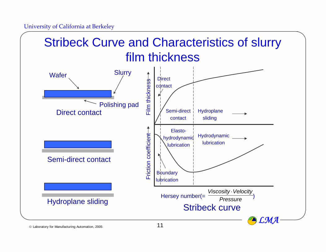
Stribeck Curve and Characteristics of slurry film thickness
Fric
tion
c oef
ficie
ntFi
lm th
ickn
ess
PressureVelocityViscosity ⋅
Hersey number(= )
Hydrodynamiclubrication
Elasto-hydrodynamic
lubrication
Boundarylubrication
Directcontact
Semi-directcontact
Hydroplanesliding
Stribeck curve
Polishing pad
Wafer Slurry
Direct contact
Semi-direct contact
Hydroplane sliding

12LMA
© Laboratory for Manufacturing Automation, 2005
University of California at Berkeley
Gap effects on “mechanics”
Pad-based removal
Slurry-based removal
‘Small’ gap
‘Big’ gap
Silicon wafer
Polishing padAbrasive particle
Delaminated by brushing
Eroded surface by chemical reaction--- softening
Silicon wafer
Polishing pad
Abrasive particles
13LMA
© Laboratory for Manufacturing Automation, 2005
University of California at Berkeley
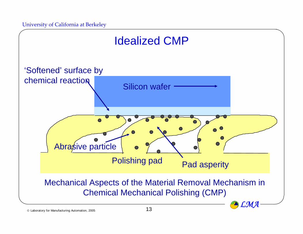
Idealized CMP
Silicon wafer
Polishing pad
Abrasive particle
‘Softened’ surface by chemical reaction
Pad asperity
Mechanical Aspects of the Material Removal Mechanism in Chemical Mechanical Polishing (CMP)
14LMA
© Laboratory for Manufacturing Automation, 2005
University of California at Berkeley
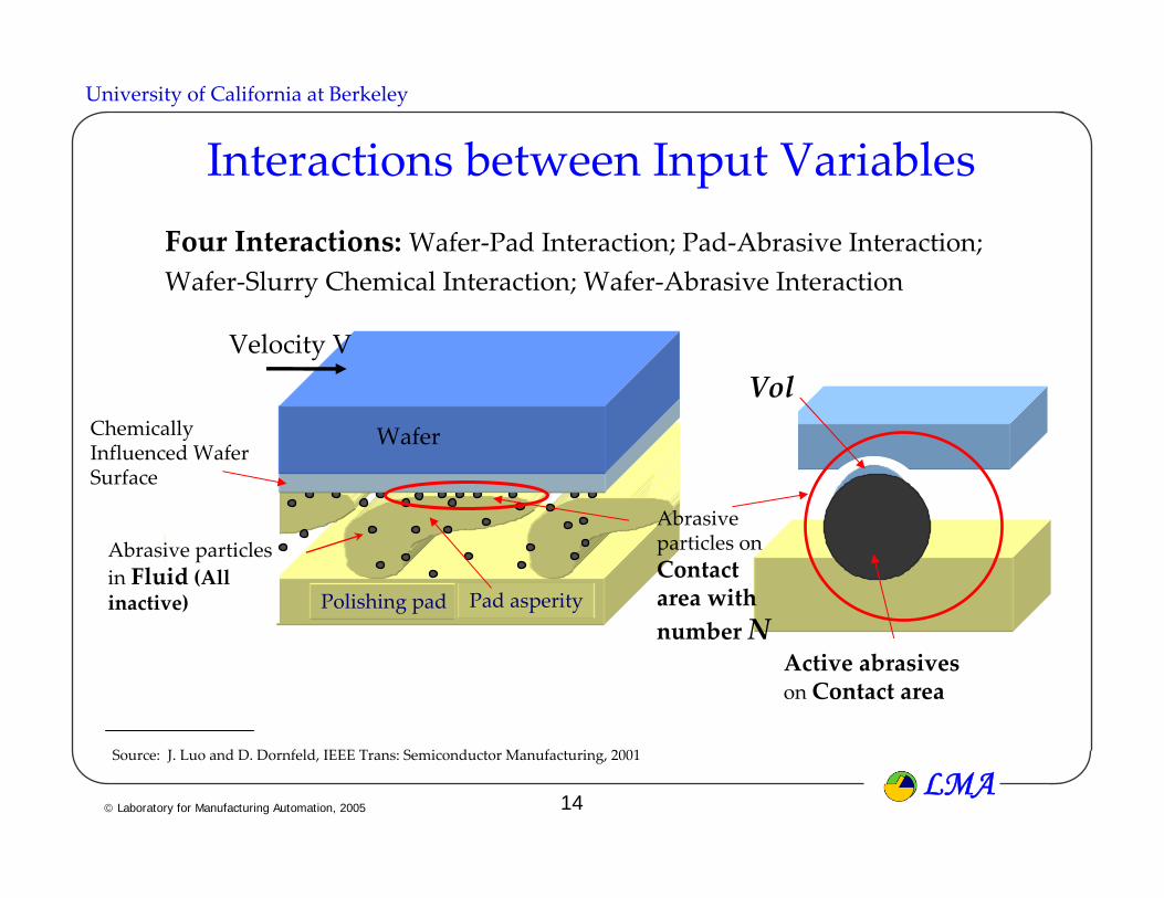
Interactions between Input VariablesFour Interactions:Wafer‐Pad Interaction; Pad‐Abrasive Interaction; Wafer‐Slurry Chemical Interaction; Wafer‐Abrasive Interaction
Polishing pad
Abrasive particles in Fluid (All inactive) Pad asperity
Active abrasiveson Contact area
VolChemically Influenced Wafer Surface
Wafer
Abrasive particles on Contact area with number N
Source: J. Luo and D. Dornfeld, IEEE Trans: Semiconductor Manufacturing, 2001
Velocity V
15LMA
© Laboratory for Manufacturing Automation, 2005
University of California at Berkeley
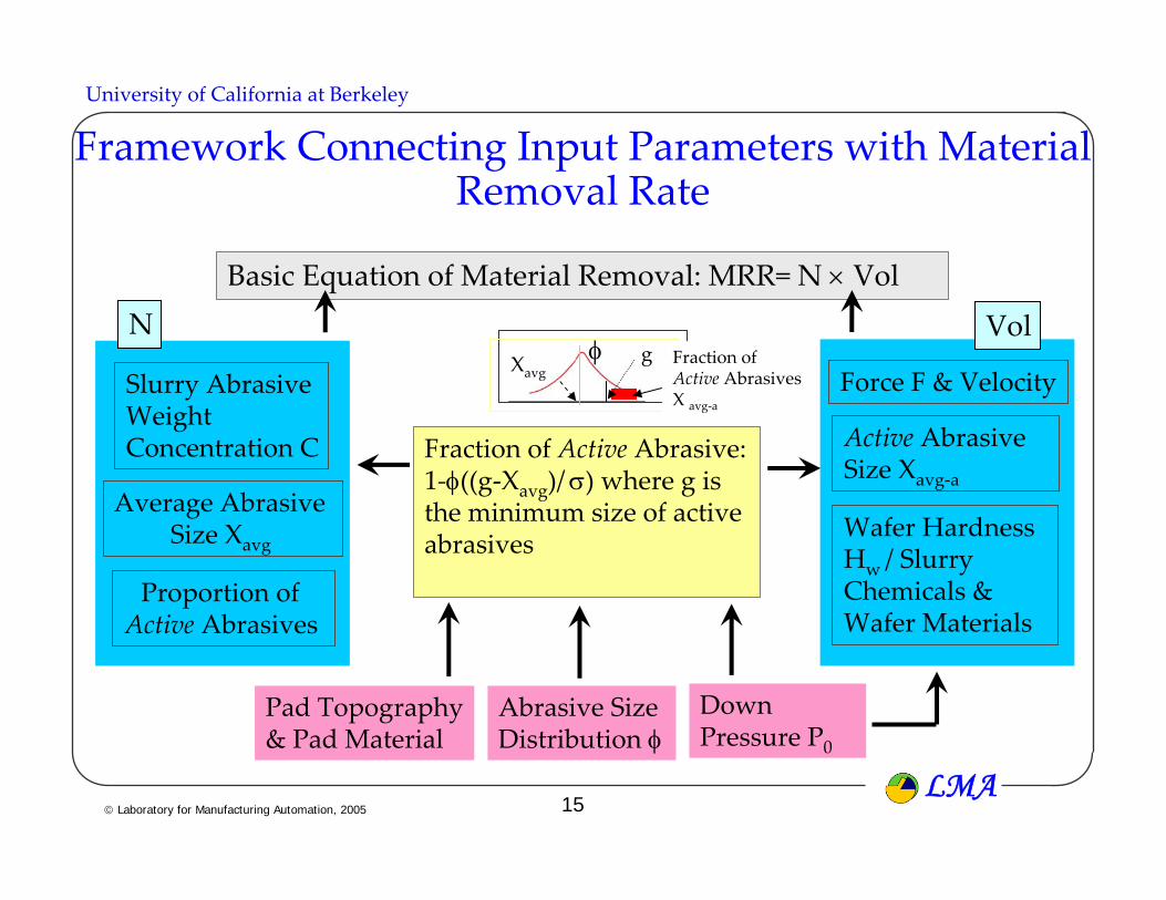
Framework Connecting Input Parameters with Material Removal Rate
Slurry Abrasive WeightConcentration C Fraction of Active Abrasive:
1‐φ((g‐Xavg)/σ) where g is the minimum size of active abrasives
Force F & Velocity
Wafer Hardness Hw / Slurry Chemicals & Wafer Materials
Vol
Active Abrasive Size Xavg‐a
Basic Equation of Material Removal: MRR= N × Vol
Average Abrasive Size Xavg
Proportion of Active Abrasives
N
Pad Topography& Pad Material
Abrasive SizeDistribution φ
Down Pressure P0
gXavgφ Fraction of
Active Abrasives X avg‐a
16LMA
© Laboratory for Manufacturing Automation, 2005
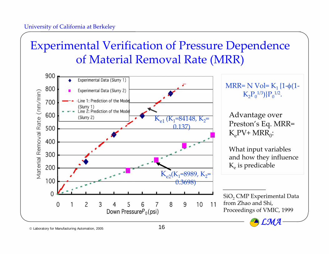
University of California at Berkeley
Ke1 (K1=84148, K2= 0.137)
Experimental Verification of Pressure Dependence of Material Removal Rate (MRR)
Advantage over Preston’s Eq. MRR= KePV+ MRR0:
What input variables and how they influence Ke is predicable
MRR= N Vol= K1 {1‐φ(1‐K2P0
1/3)}P01/2.
Ke2(K1=8989, K2= 0.3698)
SiO2 CMP Experimental Data from Zhao and Shi, Proceedings of VMIC, 1999
17LMA
© Laboratory for Manufacturing Automation, 2005
University of California at Berkeley
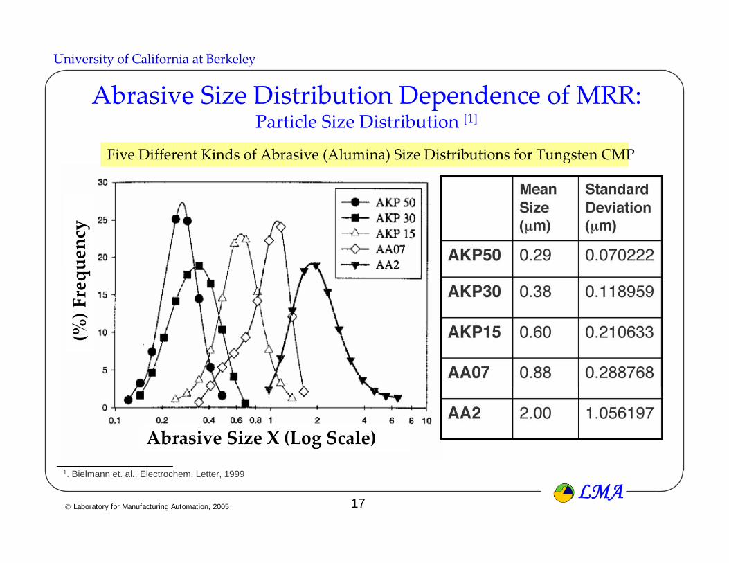
Abrasive Size Distribution Dependence of MRR:Particle Size Distribution [1]
Five Different Kinds of Abrasive (Alumina) Size Distributions for Tungsten CMP
1. Bielmann et. al., Electrochem. Letter, 1999
Abrasive Size X (Log Scale)
(%) Frequency

18LMA
© Laboratory for Manufacturing Automation, 2005
University of California at Berkeley
00.20.40.60.8
11.21.41.61.8
2
0 0.05 0.1 0.15 0.2 0.25 0.3
Standard Deviation (10-6m)
Nor
mal
ized
Mat
eria
l Rem
oval
Rat
e �
Xavg= 0.29umXavg=0.38umXavg=0.60umXavg=0.88umXavg=2um
Relationship between Standard Deviation and MRR Based on Model Prediction
Std dev influenced
Size influenced

19LMA
© Laboratory for Manufacturing Automation, 2005
University of California at Berkeley
Pattern-Density Dependency Model
InterLevel Dielectric Case (single material)
K
K/densityUp Area
0Down Area
Time
pad
oxide
pad
oxide
Same Pattern Density
Different Orientations
Source: MIT
MRR
20LMA
© Laboratory for Manufacturing Automation, 2005
University of California at Berkeley
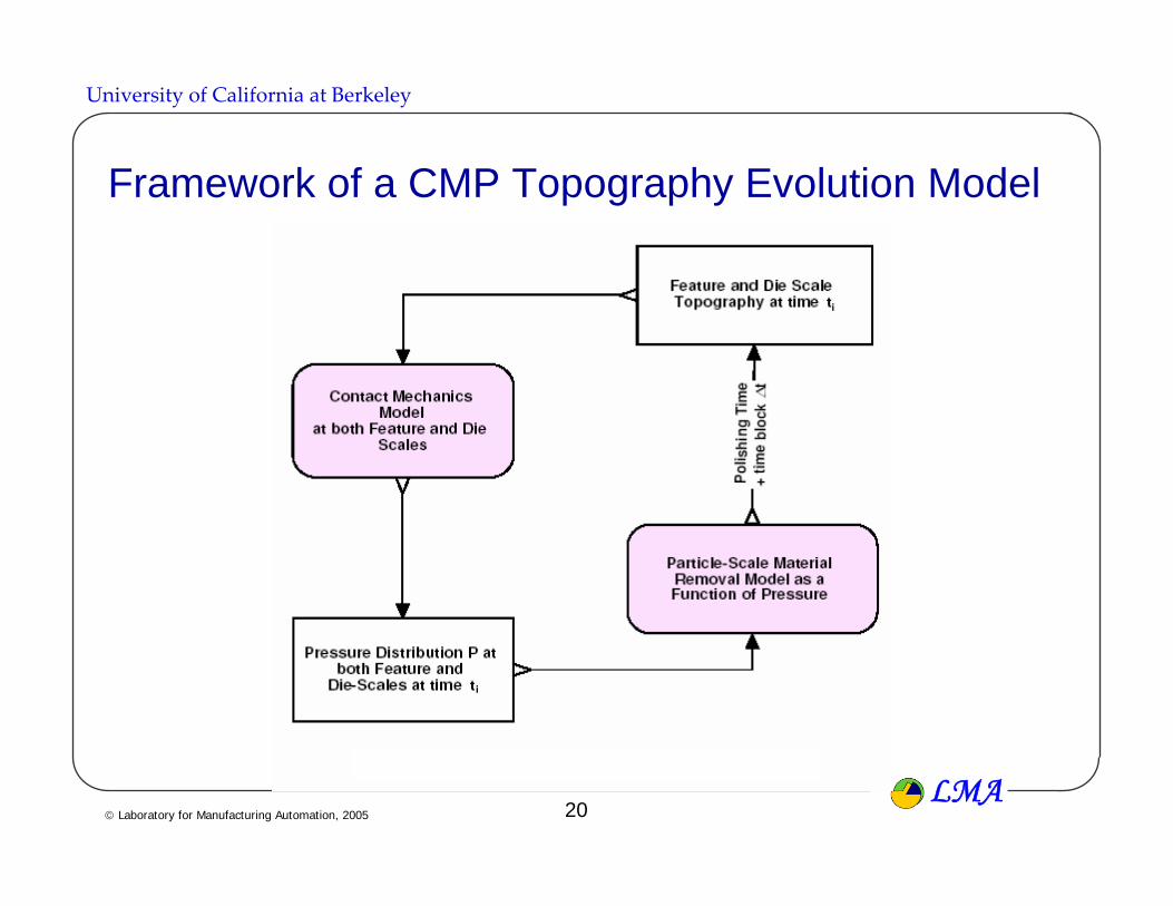
Framework of a CMP Topography Evolution Model
LMA© Laboratory for Manufacturing Automation, 2005
University of California at Berkeley
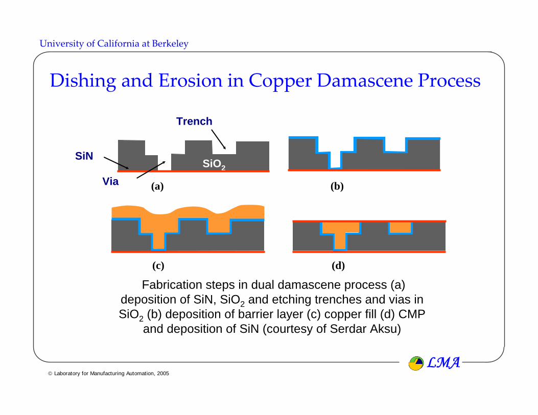
Dishing and Erosion in Copper Damascene Process
Via
Trench
SiO2SiN
(a) (b)
(c) (d)
Fabrication steps in dual damascene process (a) deposition of SiN, SiO2 and etching trenches and vias in SiO2 (b) deposition of barrier layer (c) copper fill (d) CMP
and deposition of SiN (courtesy of Serdar Aksu)

22LMA
© Laboratory for Manufacturing Automation, 2005
University of California at Berkeley
Definition of Feature‐Scale Topography
(a) (b)
(a) Feature scale topography before dielectric material is exposed and (b) feature scale topography after dielectric
material is exposed
Wcu
S
H
Wox
Copper Dishing d = S
Oxide Erosion e
H= Hox
Hox=Hox0
Hcu Copper Thinning

23LMA
© Laboratory for Manufacturing Automation, 2005
University of California at Berkeley
Kd
Kf
(a) (b) (c) (d)
η
E E η E1
η1
E2 η2
E
Models of Polishing Pad
Linear Elastic and Linear ViscoElastic Models
Separated Models of Pad Bulk and Asperities
24LMA
© Laboratory for Manufacturing Automation, 2005
University of California at Berkeley
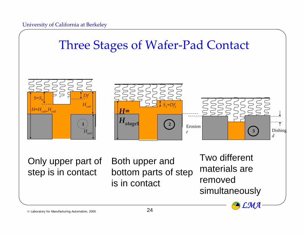
Dishing d
3Erosion e
21
Df
S1=Df1
S=S0
H=Hcu0+Hox0 H= Hstage1
Hcu0
Hox0
Three Stages of Wafer‐Pad Contact
Only upper part of step is in contact
Both upper and bottom parts of step is in contact
Two different materials are removed simultaneously

25LMA
© Laboratory for Manufacturing Automation, 2005
University of California at Berkeley
0 20 40 60 80 100 120 140 160 180 2000
50
100
150
200
250
300
350
400
450
500
Polishing Time t (second)
Ste
p H
eigh
t S (n
m)
PDi= 0.1PDi= 0.2PDi= 0.3PDi= 0.4PDi= 0.5PDi= 0.6PDi= 0.7PDi= 0.8PDi= 0.9
0 20 40 60 80 100 120 140 160 180 2000
50
100
150
200
250
300
350
400
450
500
Polishing Time t (second)
Ste
p H
eigh
t S (n
m)
PDi= 0.1PDi= 0.2PDi= 0.3PDi= 0.4PDi= 0.5PDi= 0.6PDi= 0.7PDi= 0.8PDi= 0.9
Simulation Results of Step Height Evolution for Different Pattern Density
Linear Elastic Pad Linear Viscoelastic Pad
Step heigh
t S (n
m)
Step heigh
t S (n
m)
Planarization time (sec) Planarization time (sec)
Wcu = 100 microns
26LMA
© Laboratory for Manufacturing Automation, 2005
University of California at Berkeley
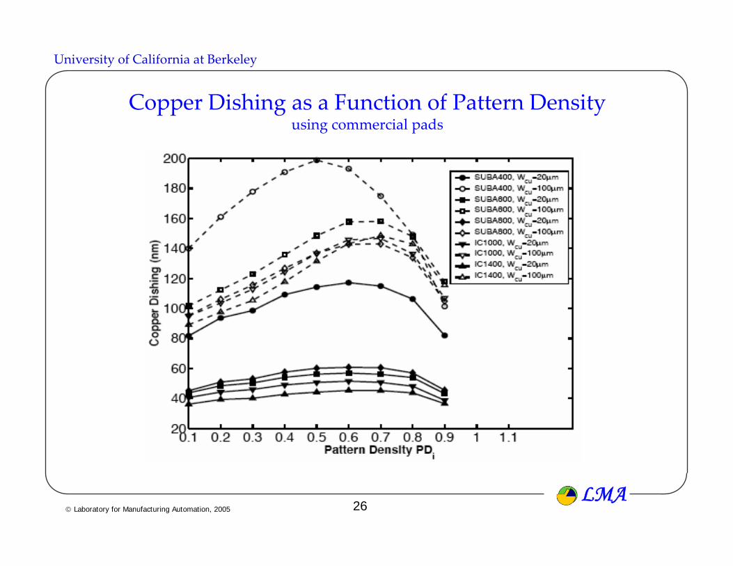
Copper Dishing as a Function of Pattern Densityusing commercial pads
27LMA
© Laboratory for Manufacturing Automation, 2005
University of California at Berkeley
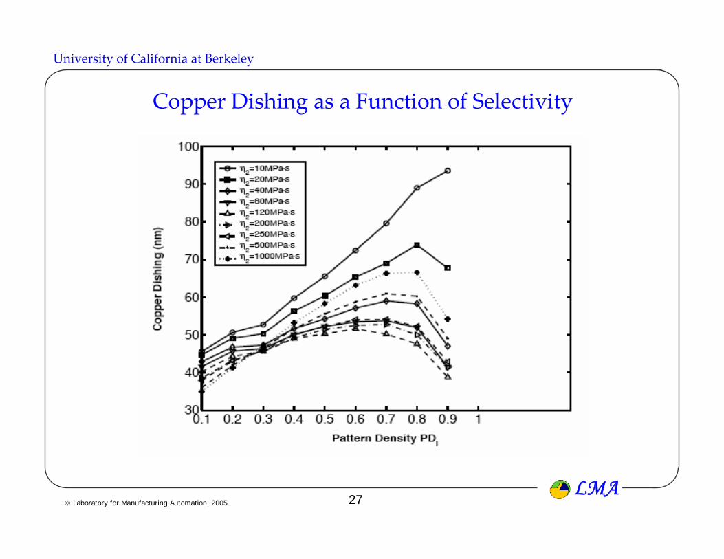
Copper Dishing as a Function of Selectivity

28LMA
© Laboratory for Manufacturing Automation, 2005
University of California at Berkeley
Effect of Pattern Density - Planarization Length (PL)
ILD
Metal linesPlanarization Length
High-density region
Low-density region
Global step

29LMA
© Laboratory for Manufacturing Automation, 2005
University of California at Berkeley
Effective pattern density
a=320um
a=640um
a=1280um
< Effective density map >
< Test pattern >
< Post CMP film thickness prediction at
die-scale >
Modeling of pattern density effects in CMP
Planarization length (window size) effect on “Up area”

LMA© Laboratory for Manufacturing Automation, 2005
University of California at Berkeley
Initial pressure distribution
Topography evolution
New pressure distribution
Contact wear model
Contact wear model
MRR model
Iteration
with time step
Die scale modeling of topography evolution during CMP
31LMA
© Laboratory for Manufacturing Automation, 2005
University of California at Berkeley
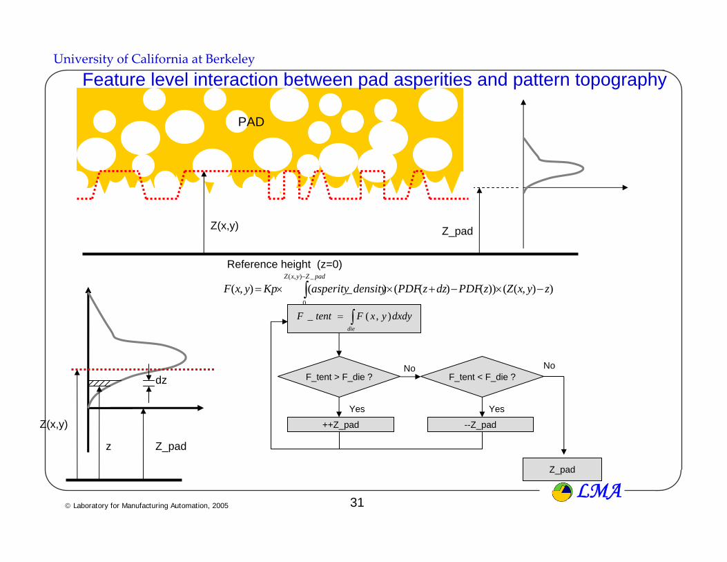
PAD
Z(x,y)
Reference height (z=0)
Z_pad
Z(x,y)
Z_padz
dz
∫−
−×−+××=padZyxZ
zyxZzPDFdzzPDFdensityasperityKpyxF_),(
0
)),(())()(()_(),(
Feature level interaction between pad asperities and pattern topography
∫=die
dxdyyxFtentF ),(_
F_tent > F_die ? F_tent < F_die ?
++Z_pad --Z_pad
No
Yes
No
Yes
Z_pad

32LMA
© Laboratory for Manufacturing Automation, 2005
University of California at Berkeley
k1
k2
221
21 kkk
kkKpad ≈+
=
Chip level interaction between pad and pattern topography
rPL
w40um
40umPattern
40um x 40um cell
∑ ∑ ⎟⎟⎟
⎠
⎞
⎜⎜⎜
⎝
⎛×
=ji
ji
E jiwjiPDjiwPD
,,
),(),(),(
θθπγ π
dPLr
Eqrrw ∫ −
−= 2
0
22
22
sin1)1(4)(
MIT model : approximation of contact wear model
LMA© Laboratory for Manufacturing Automation, 2005
University of California at Berkeley
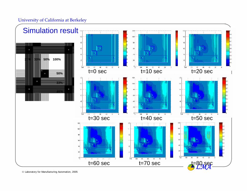
100%
50%
33%
20%
50%33%20%
t=0 sec t=10 sec t=20 sec
t=30 sec t=40 sec t=50 sec
t=60 sec t=70 sec t=80 sec
Simulation result

34LMA
© Laboratory for Manufacturing Automation, 2005
University of California at Berkeley
Pattern orientation effect on on copper dishingSiO2
Ti CuSi
Kinetic analysis of sliding direction during process time
pad rpm < wafer rpm
pad rpm = wafer rpm

35LMA
© Laboratory for Manufacturing Automation, 2005
University of California at Berkeley
• Ra = 12.5µm
• Rz = 96.7µm
• Pore diameter : 30~50 µm
• Peak to Peak : 200~300µm
100µm
45µm
-45µm100µm 300µm 500µm
(SEM, x150)
200~300µm
(White light Interferometer, x200)
Pad Characterization
36LMA
© Laboratory for Manufacturing Automation, 2005
University of California at Berkeley
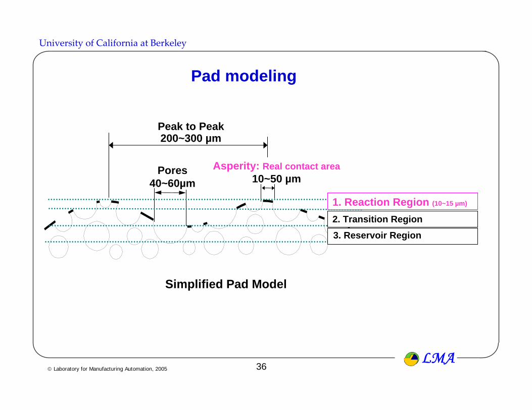
Asperity: Real contact area10~50 µm
Pores40~60µm
Simplified Pad Model
Peak to Peak200~300 µm
1. Reaction Region (10~15 µm)
2. Transition Region3. Reservoir Region
Pad modeling
37LMA
© Laboratory for Manufacturing Automation, 2005
University of California at Berkeley
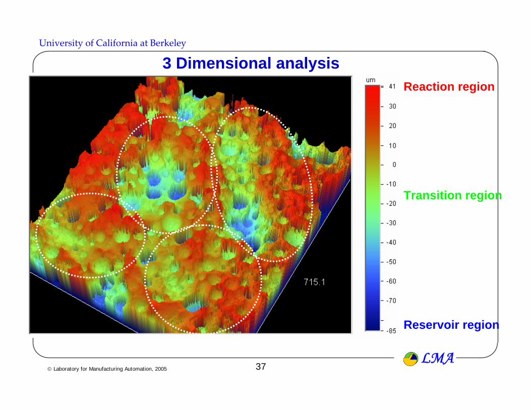
3 Dimensional analysisReaction region
Reservoir region
Transition region

38LMA
© Laboratory for Manufacturing Automation, 2005
University of California at Berkeley
2D and 3D image of reaction region
• Contact area : 10-50µm
• Ratio of real contact area : 10-15%
• Spherical or conical shape edge
• Stress concentration when compressed
2 dimensional image (w/o pressure) 3 dimensional image (w/o pressure)

39LMA
© Laboratory for Manufacturing Automation, 2005
University of California at Berkeley
10 – 50 µm
Reaction region (asperity)
Reaction region – ILD CMP
• Over polishing on recess area
• Smoothing, not planarization
Defects of a conventional pad
50 µm
Large asperity
wafer
ILDRounding
10 µm
Small asperity
wafer
ILD
Over polishing
40LMA
© Laboratory for Manufacturing Automation, 2005
University of California at Berkeley
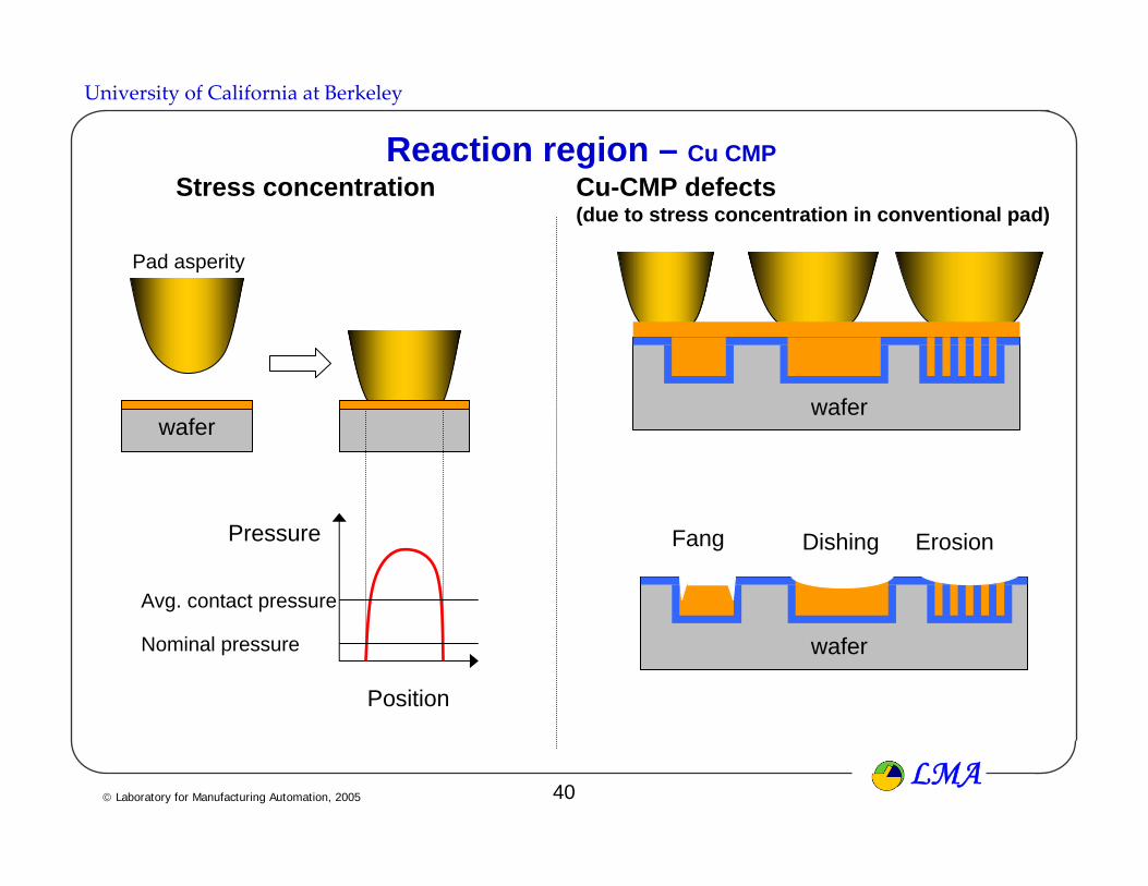
Reaction region – Cu CMP
wafer
Pressure
Position
Stress concentration
ErosionDishingFang
Cu-CMP defects (due to stress concentration in conventional pad)
Pad asperity
Nominal pressure
Avg. contact pressure
wafer
wafer

41LMA
© Laboratory for Manufacturing Automation, 2005
University of California at Berkeley
New In 3minutes
In 5minutes In 7minutes
Pad degradation

42LMA
© Laboratory for Manufacturing Automation, 2005
University of California at Berkeley
• Compatible features to abrasive
• Constant re-generation of nano
scale surface roughness
• Constant contact area
(width:10-50um)
• The ratio of real contact area
(13-17%)
• Conditioning-less CMP
• High slurry efficiency
• Stacked layer
(Hard/soft)
• Slurry channel
Nano scaleMicro scaleMacro scale
Design rules for a pad
Design rules for a pad

43LMA
© Laboratory for Manufacturing Automation, 2005
University of California at Berkeley
Soft Layer(i.e. low stiffness)
Hard Layer(i.e. high stiffness)
Channel Nano scale features
A pad design based on the rules
50-70µm
50-200µm

44LMA
© Laboratory for Manufacturing Automation, 2005
University of California at Berkeley
Wafer
Pad
Wafer
Pad
• Conditioning-less process
• High planarity & good uniformity in ILD CMP
• Without stress concentration
• Less defects in Metal CMP
AdvantagesILD CMP
Cu CMP
Expectations

45LMA
© Laboratory for Manufacturing Automation, 2005
University of California at Berkeley
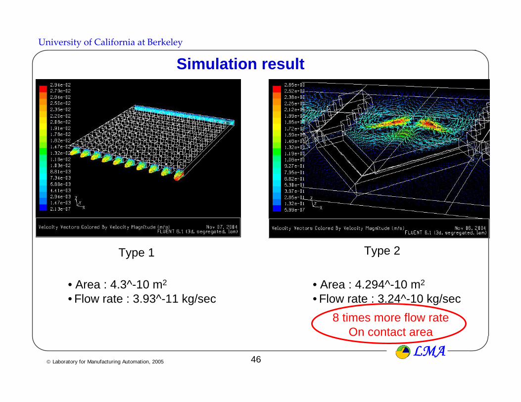
Design of new padsType 2 – With slurry guidanceType 1 – Without slurry guidance
50µm
Slurry flow direction20µm
46LMA
© Laboratory for Manufacturing Automation, 2005
University of California at Berkeley
Type 1 Type 2
• Area : 4.294^-10 m2
• Flow rate : 3.24^-10 kg/sec• Area : 4.3^-10 m2
• Flow rate : 3.93^-11 kg/sec8 times more flow rate
On contact area
Simulation result
47LMA
© Laboratory for Manufacturing Automation, 2005
University of California at Berkeley
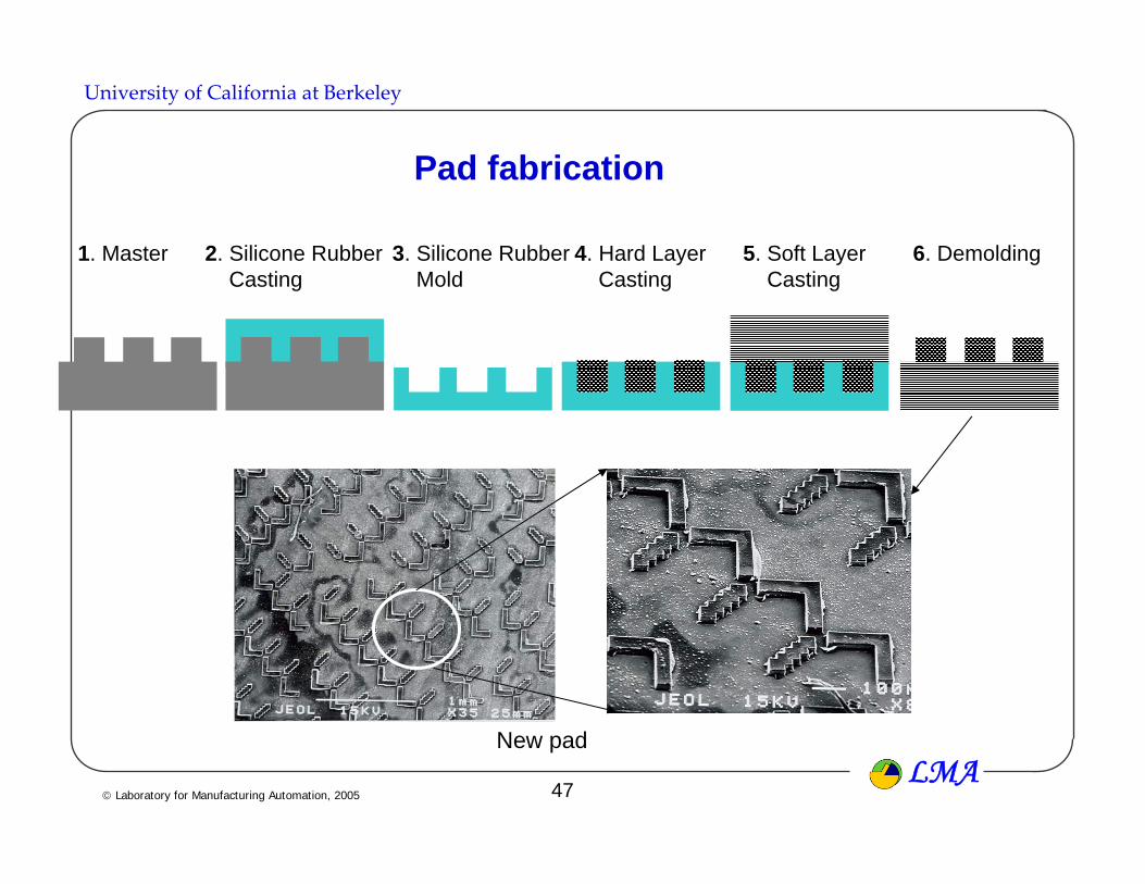
Pad fabrication
1. Master 2. Silicone Rubber Casting
3. Silicone Rubber Mold
4. Hard LayerCasting
5. Soft LayerCasting
6. Demolding
New pad
48LMA
© Laboratory for Manufacturing Automation, 2005
University of California at Berkeley
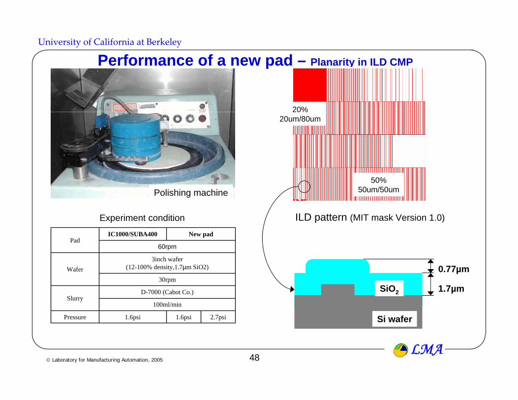
Performance of a new pad – Planarity in ILD CMP
ILD pattern (MIT mask Version 1.0)
50%50um/50um
20%20um/80um
Si wafer
SiO2
0.77µm
1.7µm
2.7psi1.6psi1.6psiPressure
100ml/min
D-7000 (Cabot Co.)Slurry
30rpm
3inch wafer (12-100% density,1.7µm SiO2)Wafer
60rpm
New padIC1000/SUBA400Pad
Polishing machine
Experiment condition
49LMA
© Laboratory for Manufacturing Automation, 2005
University of California at Berkeley
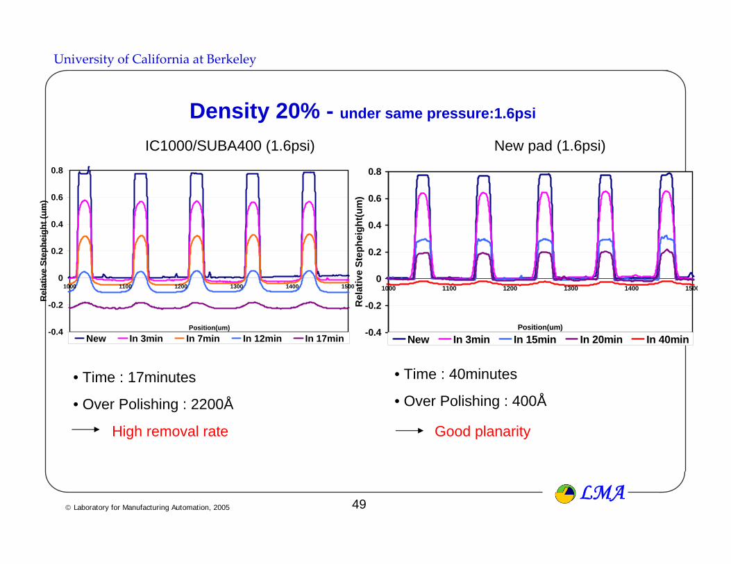
Density 20% - under same pressure:1.6psi
-0.4
-0.2
0
0.2
0.4
0.6
0.8
1000 1100 1200 1300 1400 1500
Position(um)
Rel
ativ
e St
ephe
ight
(um
)
New In 3min In 7min In 12min In 17min -0.4
-0.2
0
0.2
0.4
0.6
0.8
1000 1100 1200 1300 1400 1500
Position(um)
Rel
ativ
e St
ephe
ight
(um
)
New In 3min In 15min In 20min In 40min
• Time : 17minutes
• Over Polishing : 2200Å
• Time : 40minutes
• Over Polishing : 400Å
Good planarityHigh removal rate
IC1000/SUBA400 (1.6psi) New pad (1.6psi)
50LMA
© Laboratory for Manufacturing Automation, 2005
University of California at Berkeley
-0.4
-0.2
0
0.2
0.4
0.6
0.8
1000 1100 1200 1300 1400 1500
Position(um)
Rel
ativ
e St
ephe
ight
(um
)
New In 3min In 7min In 12min In 17min-0.4
-0.2
0
0.2
0.4
0.6
0.8
1000 1100 1200 1300 1400 1500
Position(um)
Rel
ativ
e St
ep H
eigh
t(um
)
New In 10min In 20min
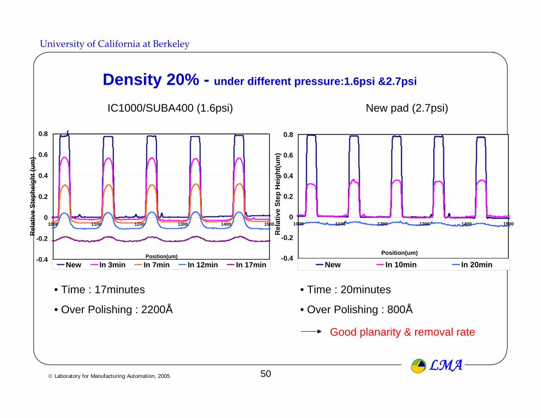
IC1000/SUBA400 (1.6psi) New pad (2.7psi)
• Time : 17minutes
• Over Polishing : 2200Å
• Time : 20minutes
• Over Polishing : 800Å
Good planarity & removal rate
Density 20% - under different pressure:1.6psi &2.7psi