modeling and simulation of jitter in pll … · events. in the case of a synthesizer, the events of...
TRANSCRIPT
WHITE PAPER
MODELING AND SIMULATION OF JITTER IN PLLFREQUENCY SYNTHESIZERS
TABLE OF CONTENTS
Abstract . . . . . . . . . . . . . . . . . . . . . . . . . . . . . . . . . . . . . . . . . . . . . . . . . . . . . . . . . . . . . . . . . . . . . . . . . . . . . . . . . . . . . . 1
Introduction . . . . . . . . . . . . . . . . . . . . . . . . . . . . . . . . . . . . . . . . . . . . . . . . . . . . . . . . . . . . . . . . . . . . . . . . . . . . . . . . . . 1
Frequency synthesis . . . . . . . . . . . . . . . . . . . . . . . . . . . . . . . . . . . . . . . . . . . . . . . . . . . . . . . . . . . . . . . . . . . . . . . . . . . . . 1
Phase-domain noise model . . . . . . . . . . . . . . . . . . . . . . . . . . . . . . . . . . . . . . . . . . . . . . . . . . . . . . . . . . . . . . . . . 2
Jitter definitions . . . . . . . . . . . . . . . . . . . . . . . . . . . . . . . . . . . . . . . . . . . . . . . . . . . . . . . . . . . . . . . . . . . . . . . . . . . . . . . 2
Cyclostationary processes . . . . . . . . . . . . . . . . . . . . . . . . . . . . . . . . . . . . . . . . . . . . . . . . . . . . . . . . . . . . . . . . . . . 2
PM jitter . . . . . . . . . . . . . . . . . . . . . . . . . . . . . . . . . . . . . . . . . . . . . . . . . . . . . . . . . . . . . . . . . . . . . . . . . . . . . . . . 3
FM jitter . . . . . . . . . . . . . . . . . . . . . . . . . . . . . . . . . . . . . . . . . . . . . . . . . . . . . . . . . . . . . . . . . . . . . . . . . . . . . . . . 3
Metrics for jitter . . . . . . . . . . . . . . . . . . . . . . . . . . . . . . . . . . . . . . . . . . . . . . . . . . . . . . . . . . . . . . . . . . . . . . . . . . 3
Phase noise . . . . . . . . . . . . . . . . . . . . . . . . . . . . . . . . . . . . . . . . . . . . . . . . . . . . . . . . . . . . . . . . . . . . . . . . . . . . . . . . . . . 4
Sources of jitter . . . . . . . . . . . . . . . . . . . . . . . . . . . . . . . . . . . . . . . . . . . . . . . . . . . . . . . . . . . . . . . . . . . . . . . . . . . . . . . . 5
Thresholds . . . . . . . . . . . . . . . . . . . . . . . . . . . . . . . . . . . . . . . . . . . . . . . . . . . . . . . . . . . . . . . . . . . . . . . . . . . . . . 5
Oscillator phase noise . . . . . . . . . . . . . . . . . . . . . . . . . . . . . . . . . . . . . . . . . . . . . . . . . . . . . . . . . . . . . . . . . . . . . . 5
Model of PLL . . . . . . . . . . . . . . . . . . . . . . . . . . . . . . . . . . . . . . . . . . . . . . . . . . . . . . . . . . . . . . . . . . . . . . . . . . . . . . . . . . 6
Modeling PM jitter . . . . . . . . . . . . . . . . . . . . . . . . . . . . . . . . . . . . . . . . . . . . . . . . . . . . . . . . . . . . . . . . . . . . . . . . 6
Modeling FM jitter . . . . . . . . . . . . . . . . . . . . . . . . . . . . . . . . . . . . . . . . . . . . . . . . . . . . . . . . . . . . . . . . . . . . . . . . 7
Efficiency of models . . . . . . . . . . . . . . . . . . . . . . . . . . . . . . . . . . . . . . . . . . . . . . . . . . . . . . . . . . . . . . . . . . . . . . . 8
Characterizing jitter . . . . . . . . . . . . . . . . . . . . . . . . . . . . . . . . . . . . . . . . . . . . . . . . . . . . . . . . . . . . . . . . . . . . . . . . . . . 12
Characterizing PM jitter . . . . . . . . . . . . . . . . . . . . . . . . . . . . . . . . . . . . . . . . . . . . . . . . . . . . . . . . . . . . . . . . . . . 12
Characterizing FM jitter . . . . . . . . . . . . . . . . . . . . . . . . . . . . . . . . . . . . . . . . . . . . . . . . . . . . . . . . . . . . . . . . . . . 14
Simulation and analysis . . . . . . . . . . . . . . . . . . . . . . . . . . . . . . . . . . . . . . . . . . . . . . . . . . . . . . . . . . . . . . . . . . . . . . . . . 14
Example . . . . . . . . . . . . . . . . . . . . . . . . . . . . . . . . . . . . . . . . . . . . . . . . . . . . . . . . . . . . . . . . . . . . . . . . . . . . . . . . . . . . . 14
Conclusion . . . . . . . . . . . . . . . . . . . . . . . . . . . . . . . . . . . . . . . . . . . . . . . . . . . . . . . . . . . . . . . . . . . . . . . . . . . . . . . . . . . 16
Acknowledgements . . . . . . . . . . . . . . . . . . . . . . . . . . . . . . . . . . . . . . . . . . . . . . . . . . . . . . . . . . . . . . . . . . . . . . . . . . . . 17
References . . . . . . . . . . . . . . . . . . . . . . . . . . . . . . . . . . . . . . . . . . . . . . . . . . . . . . . . . . . . . . . . . . . . . . . . . . . . . . . . . . . 17
TABLE OF FIGURES
Figure 1 Block diagram of a frequency synthesizer . . . . . . . . . . . . . . . . . . . . . . . . . . . . . . . . . . . . . . . . . . . . . . . . 1
Figure 2 Linear time-invariant phase-domain model of Figure 1 synthesizer . . . . . . . . . . . . . . . . . . . . . . . . . . . . 2
Figure 3 Long-term jitter (Ji) for a PLL as a function of the number of cycles . . . . . . . . . . . . . . . . . . . . . . . . . . . . 4
Figure 4 Block diagram of VCO behavioral model with jitter . . . . . . . . . . . . . . . . . . . . . . . . . . . . . . . . . . . . . . . . . 8
Figure 5 Effects of jitter on reference signals . . . . . . . . . . . . . . . . . . . . . . . . . . . . . . . . . . . . . . . . . . . . . . . . . . . . 12
Figure 6 A limiter is applied to driven-block output to suppress noise outside of active transitions . . . . . . . . . 13
Figure 7 Closed-loop (CL) versus open-loop (OL) noise at VCO output when only the reference oscillator exhibits jitter . . . . . . . . . . . . . . . . . . . . . . . . . . . . . . . . . . . . . . . . . . . . . . . . . . . . . . . . . . . . . . 15
Figure 8 Closed-loop (CL) versus open-loop (OL) noise at VCO output when only the VCO exhibits jitter . . . . . 16
Figure 9 Closed-loop (CL) versus open-loop (OL) noise at VCO output when only the PFD/CP, FDM , and FDN exhibit jitter . . . . . . . . . . . . . . . . . . . . . . . . . . . . . . . . . . . . . . . . . . . . . . . . . . . . . . . . . . 16
Figure 10 Closed-loop versus open-loop noise performance of PLL individual components . . . . . . . . . . . . . . . . . 16
Figure 11 Long-term jitter (Ji) of closed-loop PLL as a function of observation interval . . . . . . . . . . . . . . . . . . . . 16
LIST OF TABLES
Table 1: Characteristics of PM and FM jitter . . . . . . . . . . . . . . . . . . . . . . . . . . . . . . . . . . . . . . . . . . . . . . . . . . . . . . 3
Table 2: Characteristics of VCO output relative to output of FDN . . . . . . . . . . . . . . . . . . . . . . . . . . . . . . . . . . . . 11
TABLE OF LISTINGS
Listing I: Frequency divider that models PM jitter . . . . . . . . . . . . . . . . . . . . . . . . . . . . . . . . . . . . . . . . . . . . . . . . . . 6
Listing II: PFD/CP model with PM jitter . . . . . . . . . . . . . . . . . . . . . . . . . . . . . . . . . . . . . . . . . . . . . . . . . . . . . . . . . . . 7
Listing III: Fixed-frequency oscillator with FM jitter . . . . . . . . . . . . . . . . . . . . . . . . . . . . . . . . . . . . . . . . . . . . . . . . . 8
Listing VI: VCO model with FM jitter . . . . . . . . . . . . . . . . . . . . . . . . . . . . . . . . . . . . . . . . . . . . . . . . . . . . . . . . . . . . . 9
Listing V: Quadrature differential VCO model that includes FM jitter . . . . . . . . . . . . . . . . . . . . . . . . . . . . . . . . . . . 9
Listing VI: Fixed-frequency oscillator with FM and PM jitter . . . . . . . . . . . . . . . . . . . . . . . . . . . . . . . . . . . . . . . . . . 10
Listing VII: PFD/CP without jitter . . . . . . . . . . . . . . . . . . . . . . . . . . . . . . . . . . . . . . . . . . . . . . . . . . . . . . . . . . . . . . . . 10
Listing VIII: VCO with FDN . . . . . . . . . . . . . . . . . . . . . . . . . . . . . . . . . . . . . . . . . . . . . . . . . . . . . . . . . . . . . . . . . . . . . 11
Listing IX: Limiter used to characterize PM jitter in binary signals . . . . . . . . . . . . . . . . . . . . . . . . . . . . . . . . . . . . . 13
Listing X: MATLAB script used for computing Sφ(ƒm ) . . . . . . . . . . . . . . . . . . . . . . . . . . . . . . . . . . . . . . . . . . . . . . . 15
Listing XI: Spectre netlist for PLL synthesizer . . . . . . . . . . . . . . . . . . . . . . . . . . . . . . . . . . . . . . . . . . . . . . . . . . . . . . 15
1
Abstract — A methodology is presented for predictingthe jitter performance of a Phase-Locked Loop (PLL)using simulation that is both accurate and efficient.The methodology begins by characterizing the noisebehavior of the blocks that make up the PLL usingtransistor-level simulation. For each block, the jitter isextracted and provided as a parameter to behavioralmodels for inclusion in a high-level simulation of theentire PLL. This approach is efficient enough to beapplied to PLLs acting as frequency synthesizers withlarge divide ratios.
I. INTRODUCTION
Phase-locked loops (PLLs) are used in wireless receiversto implement a variety of functions, such as frequencysynthesis, clock recovery, and demodulation. One of themajor concerns in the design of PLLs is noise or jitter per-formance. Jitter from the PLL directly acts to degrade thenoise floor and selectivity of a transceiver.
Demir proposed an approach for simulating PLLs wherebya PLL is described using behavioral models simulated at ahigh level [1,2]. The models are written such that theyinclude jitter in an efficient way. He also devised a power-ful new simulation algorithm that is capable of character-izing the circuit-level noise behavior of blocks that makeup a PLL that is based on solving a set of nonlinear sto-chastic differential equations [3, 4]. Finally, he gave for-mulas that can be used to convert the results of the noisesimulations on the individual blocks into values for the jit-ter parameters for the corresponding behavioral models[5]. This approach provides accurate and efficient predic-tion of PLL jitter behavior once the noise behavior of theblocks has been characterized. However, it requires the useof an experimental simulator that is not readily available.
This paper presents the relevant ideas of Demir, but whilehe focussed on presenting the conceptual aspects of mod-eling and simulating jitter in PLLs, this paper concentrates
more on the practical aspects. It presents all the informa-tion a designer would need to predict the noise and jitter ofa PLL synthesizer. The jitter extraction methodology isbased on the commercially available SpectreRF simulator[17,18] and presents behavioral models for Verilog-A, astandard, non-proprietary analog behavioral modeling lan-guage [6, 14]. Both SpectreRF and Verilog-A are optionsto the Spectre circuit simulator [12], available fromCadence Design Systems.1
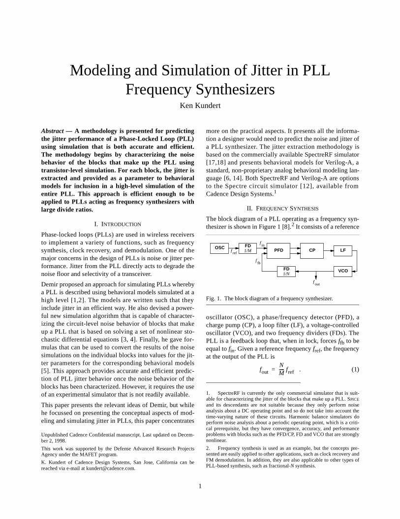
II. FREQUENCY SYNTHESIS
The block diagram of a PLL operating as a frequency syn-thesizer is shown in Figure 1 [8].2 It consists of a reference
oscillator (OSC), a phase/frequency detector (PFD), acharge pump (CP), a loop filter (LF), a voltage-controlledoscillator (VCO), and two frequency dividers (FDs). ThePLL is a feedback loop that, when in lock, forces ffb to beequal to fin. Given a reference frequency fref, the frequencyat the output of the PLL is
. (1)
1. SpectreRF is currently the only commercial simulator that is suit-able for characterizing the jitter of the blocks that make up a PLL. SPICE
and its descendants are not suitable because they only perform noiseanalysis about a DC operating point and so do not take into account thetime-varying nature of these circuits. Harmonic balance simulators doperform noise analysis about a periodic operating point, which is a criti-cal prerequisite, but they have convergence, accuracy, and performanceproblems with blocks such as the PFD/CP, FD and VCO that are stronglynonlinear.
2. Frequency synthesis is used as an example, but the concepts pre-sented are easily applied to other applications, such as clock recovery andFM demodulation. In addition, they are also applicable to other types ofPLL-based synthesis, such as fractional-N synthesis.
Unpublished Cadence Confidential manuscript. Last updated on Decem-ber 2, 1998.
This work was supported by the Defense Advanced Research ProjectsAgency under the MAFET program.
K. Kundert of Cadence Design Systems, San Jose, California can bereached via e-mail at [email protected].
Fig. 1. The block diagram of a frequency synthesizer.
PFD CP LF
VCO
OSC FD1/M
FD1/N
fref
fin
ffb
outf
foutNM----- fref=
Modeling and Simulation of Jitter in PLL Frequency Synthesizers
Ken Kundert
2 KUNDERT
DRAFT
By choosing the frequency divide ratios and the referencefrequency appropriately, the synthesizer generates an out-put signal at the desired frequency that inherits much ofthe stability of the reference oscillator. In RF transceivers,this architecture is used to generate the local oscillator(LO) at a programmable frequency, which tunes the trans-ceiver to the desired channel.
A. Phase-Domain Noise Model
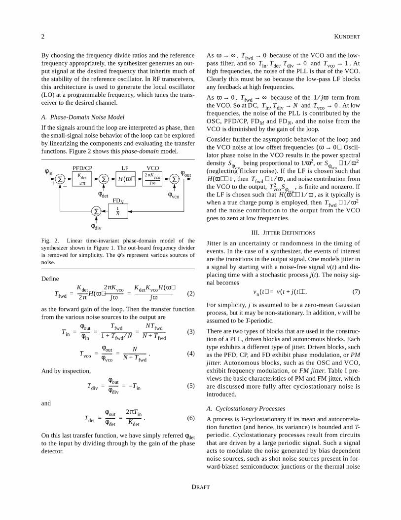
If the signals around the loop are interpreted as phase, thenthe small-signal noise behavior of the loop can be exploredby linearizing the components and evaluating the transferfunctions. Figure 2 shows this phase-domain model.
Define
(2)
as the forward gain of the loop. Then the transfer functionfrom the various noise sources to the output are
(3)
. (4)
And by inspection,
(5)
and
. (6)
On this last transfer function, we have simply referred φdetto the input by dividing through by the gain of the phasedetector.
As , because of the VCO and the low-pass filter, and so and . Athigh frequencies, the noise of the PLL is that of the VCO.Clearly this must be so because the low-pass LF blocksany feedback at high frequencies.
As , because of the term fromthe VCO. So at DC, and . At lowfrequencies, the noise of the PLL is contributed by theOSC, PFD/CP, FDM and FDN, and the noise from theVCO is diminished by the gain of the loop.
Consider further the asymptotic behavior of the loop andthe VCO noise at low offset frequencies . Oscil-lator phase noise in the VCO results in the power spectraldensity being proportional to 1/ω2, or (neglecting flicker noise). If the LF is chosen such that
, then , and noise contribution fromthe VCO to the output, , is finite and nonzero. Ifthe LF is chosen such that , as it typically iswhen a true charge pump is employed, then and the noise contribution to the output from the VCOgoes to zero at low frequencies.
III. JITTER DEFINITIONS
Jitter is an uncertainty or randomness in the timing ofevents. In the case of a synthesizer, the events of interestare the transitions in the output signal. One models jitter ina signal by starting with a noise-free signal v(t) and dis-placing time with a stochastic process j(t). The noisy sig-nal becomes
. (7)
For simplicity, j is assumed to be a zero-mean Gaussianprocess, but it may be non-stationary. In addition, v will beassumed to be T-periodic.
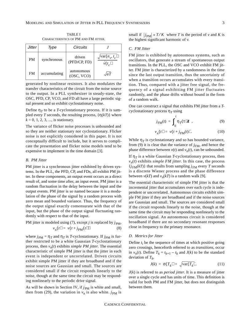
There are two types of blocks that are used in the construc-tion of a PLL, driven blocks and autonomous blocks. Eachtype exhibits a different type of jitter. Driven blocks, suchas the PFD, CP, and FD exhibit phase modulation, or PMjitter. Autonomous blocks, such as the OSC and VCO,exhibit frequency modulation, or FM jitter. Table I pre-views the basic characteristics of PM and FM jitter, whichare discussed more fully after cyclostationary noise isintroduced.
A. Cyclostationary Processes
A process is T-cyclostationary if its mean and autocorrela-tion function (and hence, its variance) is bounded and T-periodic. Cyclostationary processes result from circuitsthat are driven by a large periodic signal. Such a signalacts to modulate the noise generated by bias dependentnoise sources, such as shot noise sources present in for-ward-biased semiconductor junctions or the thermal noise
Fig. 2. Linear time-invariant phase-domain model of thesynthesizer shown in Figure 1. The out-board frequency divideris removed for simplicity. The φ ’s represent various sources ofnoise.
H ω( )2πKvco
j ω--------------------
LF VCOKdet2π-----------
1N----
ΣPFD/CP
FDN
ΣΣ
Σ
φdiv
φin
φvco
φout
φdet
–+
Tfwd
Kdet
2π----------H ω( )2πKvco
jω------------------KdetKvcoH ω( )
jω-----------------------------------= =
Tin
φout
φin---------
Tfwd
1 Tfwd N⁄+----------------------------
NTfwd
N Tfwd+---------------------= = =
Tvco
φout
φvco----------
NN Tfwd+---------------------= =
Tdiv
φout
φdiv--------- Tin–= =
Tdet
φout
φdet---------
2πTin
Kdet--------------= =
ω ∞→ Tfwd 0→Tin Tdet Tdiv, , 0→ Tvco 1→
ω 0→ Tfwd ∞→ 1 jω⁄Tin Tdiv, N→ Tvco 0→
ω 0→( )
SφvcoSφvco
1 ω2⁄∼
H ω( ) 1∼ Tfwd 1 ω⁄∼Tvco
2 SφvcoH ω( ) 1 ω⁄∼
Tfwd 1 ω2⁄∼
vn t( ) v t j t( )+( )=
MODELING AND SIMULATION OF JITTER IN PLL FREQUENCY SYNTHESIZERS 3
CADENCE CONFIDENTIAL
generated by nonlinear resistors. It also modulates thetransfer characteristics of the circuit from the noise sourceto the output. In a PLL synthesizer in steady-state, theOSC, PFD, CP, VCO, and FD all have a large periodic sig-nal present and so exhibit cyclostationary noise.
Define ηT to be a T-cyclostationary process. If it is sam-pled every T seconds, the resulting process, {η(kT)} wherek = 0, 1, 2, 3, ..., is stationary.
The variance of flicker noise processes is unbounded andso they are neither stationary nor cyclostationary. Flickernoise is not explicitly considered in this paper. It is notconceptually difficult to include, but it serves to compli-cate the presentation and flicker noise models tend to beexpensive to implement in the time domain [3].
B. PM Jitter
PM jitter is a synchronous jitter exhibited by driven sys-tems. In the PLL, the PFD, CP, and FDs, all exhibit PM jit-ter. In these components, an output event occurs as a directresult of, and some time after, an input event. PM jitter is arandom fluctuation in the delay between the input and theoutput events. PM jitter is so named because it is a modu-lation of the phase of the signal by a random process withzero mean and bounded variance. Thus, the frequency ofthe output signal exactly comensurate with that of theinput, but the phase of the output signal fluctuating ran-domly with respect to that of the input.
PM jitter is modeled using (7), except j is replaced by j PM,
(8)
where jPM = ηT and ηT is T-cyclostationary. If jPM is fur-ther restricted to be a white Gaussian T-cyclostationaryprocess, then vn(t) exhibits simple PM jitter. The essentialcharacteristic of simple PM jitter is that the jitter in eachevent is independent or uncorrelated. Driven circuitsexhibit simple PM jitter if they are broadband and if thenoise sources are Gaussian and small. The sources areconsidered small if the circuit responds linearly to thenoise, though at the same time the circuit may be respond-ing nonlinearly to the periodic drive signal.
As will be shown in Section IV, if j PM is white and small,then from (29), the variation in vn is also white. j PM is
small if where T is the period of v and K isthe highest significant harmonic of v.
C. FM Jitter
FM jitter is exhibited by autonomous systems, such asoscillators, that generate a stream of spontaneous outputtransitions. In the PLL, the OSC and VCO exhibit FM jit-ter. FM jitter is characterized by a randomness in the timesince the last output transition, thus the uncertainty ofwhen a transition occurs accumulates with every transi-tion. Thus, compared with a jitter free signal, the fre-quency of a signal exhibit ing FM j i tter f luctuatesrandomly, and the phase drifts without bound in the formof a random walk.
One can construct a signal that exhibits FM jitter from a T-cyclostationary process ηT using
, (9)
. (10)
While ηT is cyclostationary and so has bounded variance,from (9) it is clear that the variance of jFM, and hence thephase difference between v(t) and vn(t), can be unbounded.
If ηT is a white Gaussian T-cyclostationary process, thenvn(t) exhibits simple FM jitter. In this case, the process{ j FM(kT)} that results from sampling j FM every T secondsis a discrete Wiener process and the phase differencebetween v(kT) and vn(kT) is a random walk [9].
The essential characteristic of simple FM jitter is that theincremental jitter that accumulates over each cycle is inde-pendent or uncorrelated. Autonomous circuits exhibit sim-ple FM jitter if they are broadband and if the noise sourcesare Gaussian and small. The sources are considered smallif the circuit responds linearly to the noise, though at thesame time the circuit may be responding nonlinearly to theoscillation signal. An autonomous circuit is consideredbroadband if there are no secondary resonant responsesclose in frequency to the primary resonance.
D. Metrics for Jitter
Define ti be the sequence of times at which positive goingzero crossings, henceforth referred to as transitions, occurin vn(t). Define Tk = tk+1 – tk and J(k) to be the standarddeviation of Tk,
. (11)
J(k) is referred to as period jitter. It is a measure of jitterover a single cycle and has units of time. This definition isvalid for both PM and FM jitter, but does not distinguishbetween them.
TABLE ICHARACTERISTICS OF PM AND FM JITTER.
Jitter Type Circuits J
PM synchronousdriven
(PFD/CP, FD)
FM accumulatingautonomous (OSC, VCO)
var nv tc,( )
v· tc( )-----------------------------
aT
vn t( ) v t jPM t( )+( )=
jPM T K⁄«
jFM t( ) ηT τ( ) τd0
t
∫=
vn t( ) v t jFM t( )+( )=
J k( ) σ Tk( ) var Tk( )= =
4 KUNDERT
DRAFT
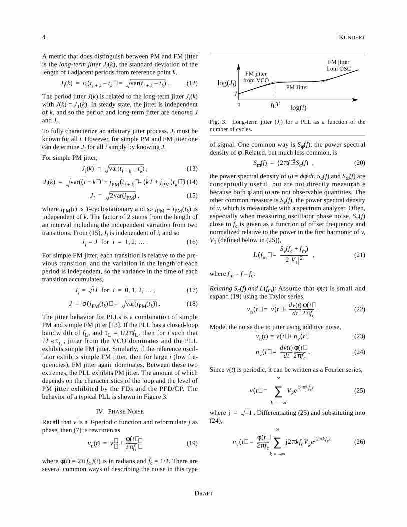
A metric that does distinguish between PM and FM jitteris the long-term jitter Ji(k), the standard deviation of thelength of i adjacent periods from reference point k,
. (12)
The period jitter J(k) is related to the long-term jitter Ji(k)with J(k) = J1(k). In steady state, the jitter is independentof k, and so the period and long-term jitter are denoted Jand Ji.
To fully characterize an arbitrary jitter process, Ji must beknown for all i. However, for simple PM and FM jitter onecan determine Ji for all i simply by knowing J.
For simple PM jitter,
, (13)
(14)
, (15)
where jPM(t) is T-cyclostationary and so jPM = jPM(tk) isindependent of k. The factor of 2 stems from the length ofan interval including the independent variation from twotransitions. From (15), Ji is independent of i, and so
. (16)
For simple FM jitter, each transition is relative to the pre-vious transition, and the variation in the length of eachperiod is independent, so the variance in the time of eachtransition accumulates,
, (17)
. (18)
The jitter behavior for PLLs is a combination of simplePM and simple FM jitter [13]. If the PLL has a closed-loopbandwidth of fL, and τL = 1/2πfL, then for i such that
, jitter from the VCO dominates and the PLLexhibits simple FM jitter. Similarly, if the reference oscil-lator exhibits simple FM jitter, then for large i (low fre-quencies), FM jitter again dominates. Between these twoextremes, the PLL exhibits PM jitter. The amount of whichdepends on the characteristics of the loop and the level ofPM jitter exhibited by the FDs and the PFD/CP. Thebehavior of a typical PLL is shown in Figure 3.
IV. PHASE NOISE
Recall that v is a T-periodic function and reformulate j asphase, then (7) is rewritten as
(19)
where φ(t) = 2π fc j(t) is in radians and fc = 1/T. There areseveral common ways of describing the noise in this type
of signal. One common way is Sφ(f), the power spectraldensity of φ. Related, but much less common, is
, (20)
the power spectral density of ω = dφ/dt. Sφ(f) and Sω(f) areconceptually useful, but are not directly measurablebecause both φ and ω are not observable quantities. Theother common measure is Sv(f), the power spectral densityof v, which is measurable with a spectrum analyzer. Often,especially when measuring oscillator phase noise, Sv(f)close to fc is given as a function of offset frequency andnormalized relative to the power in the first harmonic of v,V1 (defined below in (25)),
, (21)
where fm = f – fc.
Relating Sφ(f) and L(fm): Assume that φ(t) is small andexpand (19) using the Taylor series,
. (22)
Model the noise due to jitter using additive noise,
(23)
. (24)
Since v(t) is periodic, it can be written as a Fourier series,
(25)
where . Differentiating (25) and substituting into(24),
(26)
Ji k( ) σ ti k+ tk–( ) var ti k+ tk–( )= =
Ji k( ) var ti k+ tk–( )=
Ji k( ) var i k+( )T j+ PM ti k+( ) kT jPM tk( )+( )–( )=
Ji 2var jPM( )=
Ji J for = i 1 2 …, ,=
Ji i= J for i 0 1 2 …, , ,=
J σ jFM tk( )( ) var jFM tk( )( )= =
iT τL«
vn t( ) v tφ t( )2πfc-----------+
=
Fig. 3. Long-term jitter (Ji) for a PLL as a function of thenumber of cycles.
J
log(Ji)
log(i)
FM jitter
PM Jitter
FM jitter
fLT0
from OSC
from VCO
Sω f( ) 2πf( )2Sφ f( )=
L fm( )Sv fc fm+( )
2 V12-------------------------=
vn t( ) v t( )dv t( )
dt-----------
φ t( )2π fc-----------+=
vn t( ) v t( )= nv t( )+
nv t( )dv t( )
dt-----------
φ t( )2π fc-----------=
v t( ) Vkej2πkfct
k ∞–=
∞
∑=
j 1–=
nv t( )φ t( )2π fc----------- j2πkfcV
kej2πkfct
k ∞–=
∞
∑=
MODELING AND SIMULATION OF JITTER IN PLL FREQUENCY SYNTHESIZERS 5
CADENCE CONFIDENTIAL
. (27)
Computing the power spectral density of nv gives
(28)
(29)
Assume that Sφ(f) drops rapidly with increasing frequency,then for
. (30)
Recall that several assumptions were made in developingthis approximation. In particular, that φ(t) is small and thatSφ at low frequencies is much larger than at frequenciesnear fc and higher. The first approximation is not valid forphase noise of a free running oscillator for small fmbecause φ(t) is undergoing a random walk, and so isunbounded.
V. SOURCES OF JITTER
A. Thresholds
In systems where signals are continuous valued, an eventis usually defined as a signal crossing a threshold in a par-ticular direction. The threshold crossings of a noiselessperiodic signal, v(t), are precisely evenly spaced. However,when noise is added to the signal, vn(t) = v(t) + nv(t), eachthreshold crossing is displaced slightly. Thus, a thresholdconverts additive noise to PM jitter.
The amount of displacement in time is determined by theamplitude of the noise signal, nv(t), and the slew rate of theperiodic signal, dv(tc)/dt, as the threshold is crossed. If thenoise nv is stationary, then
(31)
where tc is the time of a threshold crossing.
Generally nv is not stationary, but cyclostationary. It isonly important to know when the noisy periodic signalvn(t) crosses the threshold, so the statistics of nv are onlysignificant at the time when vn(t) crosses the threshold,
. (32)
The jitter is computed from (31) or (32) using (16),
. (33)
B. Oscillator Phase Noise
FM jitter is strongly related to oscillator phase noise. Bothare different ways of describing the same underlying phe-nomenon. In other words, all free running oscillatorsexhibit a behavior that is generically referred to as oscilla-tor phase noise. Any noise in an autonomous system willcause the phase to drift freely because there is no referencesignal with which to lock. When the phase fluctuations aremeasured in terms of time deviation over a period, it isreferred to as FM jitter. If it is measured in terms of noisesignal amplitude as a function of frequency, it is referredto as oscillator phase noise.
Relating J and Sφ: In order to determine the period jitter Jof vn(t) for a noisy oscillator, assume that it exhibits simpleFM jitter so that η in (9) is a white Gaussian noise process(this excludes flicker noise) with a PSD of
, (34)
and an autocorrelation function of
, (35)
where δ is a Dirac delta function. Then
(36)
is a Wiener process [9], which has an autocorrelation func-tion of
. (37)
The variance of jFM over one period T is
(38)
Finally, jitter is the standard deviation of the variation inthe period, and so
. (39)
nv t( ) φ t( ) jkVke2πkfct
k ∞–=
∞
∑=
Snvf( ) kVk
2Sφ f kfc–( )
k ∞–=
∞
∑=
L fm( )Snv
fc fm+( )
2 V12----------------------------
12---
kVk
V1---------
2Sφ fm k 1–( )fc–( )
k ∞–=
∞
∑= =
fm fc«
L fm( )12---S
φfm( )≅
var jPM tc( )( )var nv( )
v· tc( )2------------------≅
var jPM tc( )( )var nv tc,( )
v· tc( )2-------------------------=
J 2var jPM tc( )( )=
Sη f( ) a=
Rη t1 t2,( ) aδ t1 t2–( )=
jFM t( ) ηT τ( ) τd0
t
∫=
RjFMt1 t2,( ) amin t1 t2,( )=
var jFM t T+( ) jFM t( )–( )
E jFM t T+( ) jFM t( )–( )2[ ]
E jFM t T+( )2 2jFM t T+( ) jFM t( ) j+FM
t( )– 2[ ]
E jFM t T+( )2[ ] 2E jFM t T+( )jFM t( )[ ]– E jFM t( )2[ ]+
RjFMt T t T+,+( ) 2RjFM
t T t,+( ) RjFMt t,( )+–
a t T+( ) 2at– at+
aT
=
=
=
=
=
=
J aT=
6 KUNDERT
DRAFT
We now have a way of relating the jitter of the oscillator tothe PSD of η. However, what is needed is to relate the jit-ter to either Sφ or L. To do so, consider simple FM jitterwritten in terms of phase,
(40)
and so from (34) and (40) the PSD of φFM(t) is
. (41)
Thus, a is the noise power in φFM where f = fc, or
. (42)
Given Sφ and fc, a is found with (41)3 and then J is foundwith (39).
Relating Sφ(f) and L(fm): The phase variation in a simpleFM jitter process is not bounded, and so (29) cannot beused to predict L(fm) of an oscillator. Demir shows that fora free-running oscillator exhibiting simple FM jitter
, (43)
which is a Lorentzian with corner frequency of
. (44)
At frequencies above the corner,
, (45)
which agrees with (30) and Vendelin [19]. Thus, in free-running oscillators at frequencies above the corner, L(fm)and Sφ(fm) are easily related.4
VI. MODEL OF PLL
The basic behavioral models for the blocks that make up aPLL are well known and so will not be discussed here inany depth [1,2]. Instead, only the techniques for adding jit-ter to the models are discussed.
Jitter is modeled in an AHDL by dithering the time atwhich events occur. This is efficient because it does notcreate any additional activity, rather it simply changes the
3. In general, (42) is not used when computing a because Sφ is notaccurately known at fc. Instead, f is chosen where Sφ is accurately known,and (41) is used.
4. When using (45) and (41) to determine a, choose f well above thecorner frequency of (44) to avoid ambiguity and well below fc to avoidthe noise from other sources that occur at these frequencies.
time when existing activity occurs. Thus, models with jit-ter can run as efficiently as those without.
A. Modeling PM Jitter
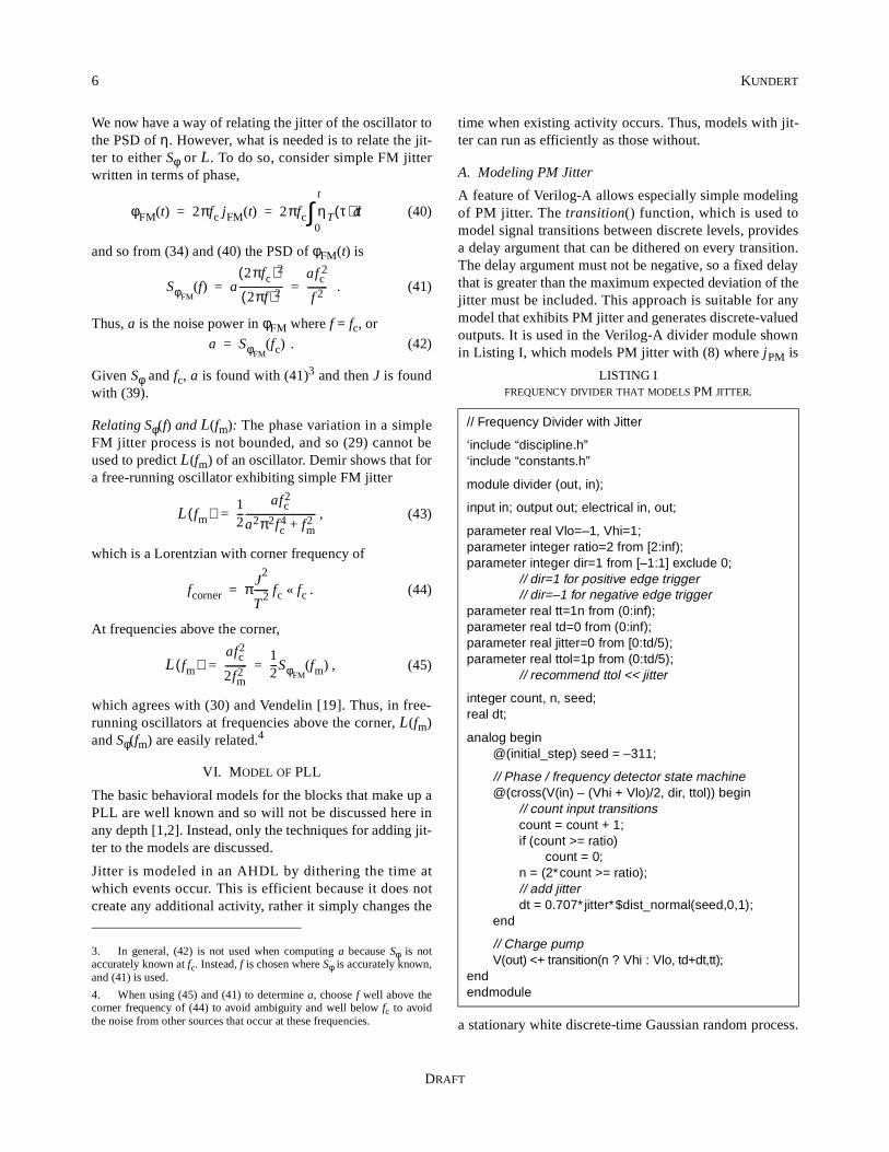
A feature of Verilog-A allows especially simple modelingof PM jitter. The transition() function, which is used tomodel signal transitions between discrete levels, providesa delay argument that can be dithered on every transition.The delay argument must not be negative, so a fixed delaythat is greater than the maximum expected deviation of thejitter must be included. This approach is suitable for anymodel that exhibits PM jitter and generates discrete-valuedoutputs. It is used in the Verilog-A divider module shownin Listing I, which models PM jitter with (8) where jPM is
a stationary white discrete-time Gaussian random process.
φFM t( ) 2πfc jFM t( ) 2πfc ηT τ( ) τd0
t
∫= =
SφFMf( ) a
2πfc( )2
2πf( )2------------------afc
2
f 2--------= =
a SφFMfc( )=
L fm( )12---
afc2
a2π2fc4 fm
2+-----------------------------=
fcorner πJ
2
T2------ fc fc«=
L fm( )afc
2
2fm2---------
12---SφFM
fm( )= =
LISTING IFREQUENCY DIVIDER THAT MODELS PM JITTER.
// Frequency Divider with Jitter
‘include “discipline.h”‘include “constants.h”
module divider (out, in);
input in; output out; electrical in, out;
parameter real Vlo=–1, Vhi=1;parameter integer ratio=2 from [2:inf);parameter integer dir=1 from [–1:1] exclude 0;
// dir=1 for positive edge trigger// dir=–1 for negative edge trigger
parameter real tt=1n from (0:inf);parameter real td=0 from (0:inf);parameter real jitter=0 from [0:td/5);parameter real ttol=1p from (0:td/5);
// recommend ttol << jitter
integer count, n, seed; real dt;
analog begin@(initial_step) seed = –311;
// Phase / frequency detector state machine@(cross(V(in) – (Vhi + Vlo)/2, dir, ttol)) begin
// count input transitionscount = count + 1;if (count >= ratio)
count = 0;n = (2∗count >= ratio);// add jitterdt = 0.707∗jitter∗$dist_normal(seed,0,1);
end
// Charge pumpV(out) <+ transition(n ? Vhi : Vlo, td+dt,tt);
endendmodule
MODELING AND SIMULATION OF JITTER IN PLL FREQUENCY SYNTHESIZERS 7
CADENCE CONFIDENTIAL
It is also used in Listing II, which models a simple PFD/CP.
Frequency Divider Model: The model, given in Listing I,operates by counting input transitions. This is done in the@cross block. The cross function triggers the @ block atthe precise moment when its first argument crosses zero inthe direction specified by the second argument. Thus, the@ block is triggered when the input crosses the thresholdin the user specified direction. The body of the @ blockincrements the count, resets it to zero when it reaches ratio,then determines if count is above or below its midpoint (nis zero if the count is below the midpoint). It also gener-ates a new random dither dT that is used later. Outside the@ block is code that executes continuously. It processes nto create the output. The value of the ?: operator is Vhi if nis 1 and Vlo if n is 0. Finally, the transition function adds afinite transition time of tt and a delay of td + dt. The finitetransition time removes the discontinuities from the signal
that could cause problems for the simulator. The jitter isembodied in dt, which varies randomly from transition totransition. The jitter J represents the variation in a period,and dt the variation of a single transition, so from (16)
, (46)
which compensates for the fact that both ends of eachinterval are varying. To avoid nonnegative delays, td mustalways be larger than dt.
PFD/CP Model: The model for a phase/frequency detec-tor combined with a charge pump is given in Listing II. Itimplements a finite-state machine with a three-level out-put, –1, 0 and +1. On every transition of the VCO input indirection dir, the output is incremented. On every transitionof the reference input in the direction dir, the output is dec-remented. If both the VCO and reference inputs are at thesame frequency, then the average value of the output isproportional to the phase difference between the two, withthe average being negative if the reference transition leadsthe VCO transition and positive otherwise [8]. As before,the time of the output transitions are randomly dithered bydt to model jitter. The output is modeled as an ideal currentsource and a finite transition time models the dead band inthe CP.
B. Modeling FM jitter
OSC Model: The delay argument of the transition() func-tion cannot be used to model FM jitter because of thecumulative nature of this type of jitter. When modeling afixed frequency oscillator, the timer() function is used asshown in Listing III. At every output transition, the nexttransition is scheduled using the timer() function to be
in the future, where δ is a unit-variancezero-mean random process and K is the number of outputtransitions per period. Typically, K = 2.
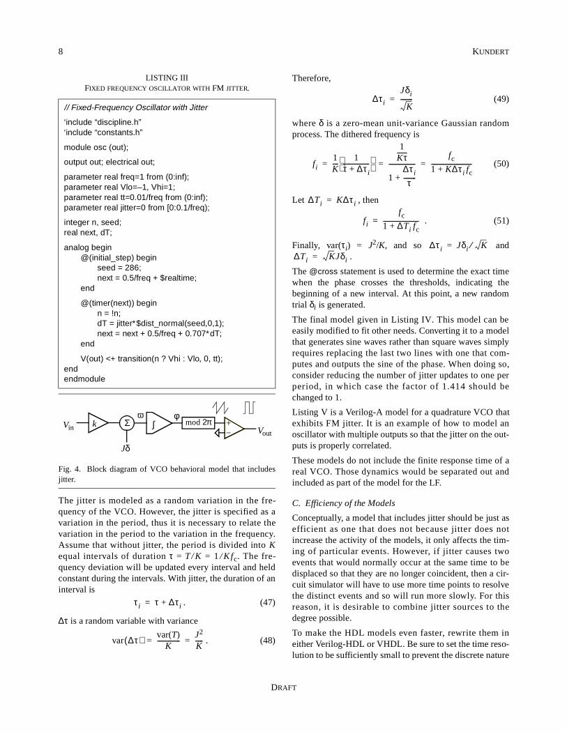
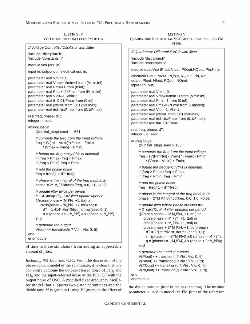
VCO Model: A VCO generates a sine or square wavewhose frequency is proportional to the input signal level.VCO models, given in Listings IV and V, are constructedusing three serial operations, as shown in Figure 4. First,the input signal is scaled to compute the desired outputfrequency. Then, the frequency is integrated to computethe output phase. Finally, the phase is used to generate thedesired output signal. The phase is computed with idtmod,a function that provides integration followed by a modulusoperation. This serves to keep the phase bounded, whichprevents a loss of numerical precision that would other-wise occur when the phase became large after a longperiod of time. Output transitions are generated when thephase passes –π/2 and π/2.
LISTING IIPFD/CP MODEL WITH PM JITTER.
// Phase-Frequency Detector & Charge Pump
`include “discipline.h”`include “constants.h”
module pfd_cp (out, ref, vco);
input ref, vco; output out; electrical ref, vco, out;
parameter real Iout=100u;parameter integer dir=1 from [–1:1] exclude 0;
// dir=1 for positive edge trigger// dir=–1 for negative edge trigger
parameter real tt=1n from (0:inf);parameter real td=0 from (0:inf);parameter real jitter=0 from [0:td/5);parameter real ttol=1p from (0:td/5);
// recommend ttol << jitter
integer state, seed;real dt;
analog begin@(initial_step) seed = 716;
@(cross(V(ref), dir, ttol)) beginif (state > –1) state = state – 1;dt = 0.707∗jitter∗$dist_normal(seed,0,1);
end
@(cross(V(vco), dir, ttol)) beginif (state < 1) state = state + 1;dt = 0.707∗jitter∗$dist_normal(seed,0,1);
end
I(out) <+ transition(Iout∗state, td + dt, tt);endendmodule
dt σ jPM tc( )( ) 2J 0.707J≅= =
T K⁄ Jδ K⁄+
8 KUNDERT
DRAFT
The jitter is modeled as a random variation in the fre-quency of the VCO. However, the jitter is specified as avariation in the period, thus it is necessary to relate thevariation in the period to the variation in the frequency.Assume that without jitter, the period is divided into Kequal intervals of duration τ = T/K = 1/K fc. The fre-quency deviation will be updated every interval and heldconstant during the intervals. With jitter, the duration of aninterval is
. (47)
∆τ is a random variable with variance
. (48)
Therefore,
(49)
where δ is a zero-mean unit-variance Gaussian randomprocess. The dithered frequency is
(50)
Let , then
. (51)
Finally, var(τi) = J2/K, and so and.
The @cross statement is used to determine the exact timewhen the phase crosses the thresholds, indicating thebeginning of a new interval. At this point, a new randomtrial δi is generated.
The final model given in Listing IV. This model can beeasily modified to fit other needs. Converting it to a modelthat generates sine waves rather than square waves simplyrequires replacing the last two lines with one that com-putes and outputs the sine of the phase. When doing so,consider reducing the number of jitter updates to one perperiod, in which case the factor of 1.414 should bechanged to 1.
Listing V is a Verilog-A model for a quadrature VCO thatexhibits FM jitter. It is an example of how to model anoscillator with multiple outputs so that the jitter on the out-puts is properly correlated.
These models do not include the finite response time of areal VCO. Those dynamics would be separated out andincluded as part of the model for the LF.
C. Efficiency of the Models
Conceptually, a model that includes jitter should be just asefficient as one that does not because jitter does notincrease the activity of the models, it only affects the tim-ing of particular events. However, if jitter causes twoevents that would normally occur at the same time to bedisplaced so that they are no longer coincident, then a cir-cuit simulator will have to use more time points to resolvethe distinct events and so will run more slowly. For thisreason, it is desirable to combine jitter sources to thedegree possible.
To make the HDL models even faster, rewrite them ineither Verilog-HDL or VHDL. Be sure to set the time reso-lution to be sufficiently small to prevent the discrete nature
LISTING IIIFIXED FREQUENCY OSCILLATOR WITH FM JITTER.
// Fixed-Frequency Oscillator with Jitter
‘include “discipline.h”‘include “constants.h”
module osc (out);
output out; electrical out;
parameter real freq=1 from (0:inf);parameter real Vlo=–1, Vhi=1;parameter real tt=0.01/freq from (0:inf);parameter real jitter=0 from [0:0.1/freq);
integer n, seed;real next, dT;
analog begin@(initial_step) begin
seed = 286;next = 0.5/freq + $realtime;
end
@(timer(next)) beginn = !n;dT = jitter∗$dist_normal(seed,0,1);next = next + 0.5/freq + 0.707∗dT;
end
V(out) <+ transition(n ? Vhi : Vlo, 0, tt);endendmodule
Fig. 4. Block diagram of VCO behavioral model that includesjitter.
k Σ ∫ mod 2π
Jδ
φVin Vout
ω
τi τ ∆τi+=
var ∆τ( ) var T( )K
---------------J2
K-----= =
∆τi
Jδi
K--------=
fi1K----
1τ ∆τi+-----------------
1
Kτ------
1∆τi
τ--------+
-----------------fc
1 K∆τi fc+--------------------------= = =
∆Ti K∆τi=
fifc
1 ∆Ti fc+-----------------------=
∆τi Jδi K⁄=∆Ti KJδi=
MODELING AND SIMULATION OF JITTER IN PLL FREQUENCY SYNTHESIZERS 9
CADENCE CONFIDENTIAL
of time in these simulators from adding an appreciableamount of jitter.
Including PM Jitter into OSC: From the discussion of thephase-domain model of the synthesizer, it is clear that onecan easily combine the output-referred noise of FDM andFDN and the input-referred noise of the PFD/CP with theoutput noise of OSC. A modified fixed-frequency oscilla-tor model that supports two jitter parameters and thedivide ratio M is given in Listing VI (more on the effect of
the divide ratio on jitter in the next section). The fmJitterparameter is used to model the FM jitter of the reference
LISTING IVVCO MODEL THAT INCLUDES FM JITTER.
// Voltage Controlled Oscillator with Jitter
‘include “discipline.h”‘include “constants.h”
module vco (out, in);
input in; output out; electrical out, in;
parameter real Vmin=0;parameter real Vmax=Vmin+1 from (Vmin:inf);parameter real Fmin=1 from (0:inf);parameter real Fmax=2∗Fmin from (Fmin:inf);parameter real Vlo=–1, Vhi=1;parameter real tt=0.01/Fmax from (0:inf);parameter real jitter=0 from [0:0.25/Fmax);parameter real ttol=1u/Fmax from (0:1/Fmax);
real freq, phase, dT;integer n, seed;
analog begin@(initial_step) seed = –561;
// compute the freq from the input voltage freq = (V(in) – Vmin)∗(Fmax – Fmin)
/ (Vmax – Vmin) + Fmin;
// bound the frequency (this is optional)if (freq > Fmax) freq = Fmax;if (freq < Fmin) freq = Fmin;
// add the phase noisefreq = freq/(1 + dT∗freq);
// phase is the integral of the freq modulo 2πphase = 2∗‘M_PI∗idtmod(freq, 0.0, 1.0, –0.5);
// update jitter twice per period// 1.414=sqrt(K), K=2 jitter updates/period@(cross(phase + ‘M_PI/2, +1, ttol) or cross(phase – ‘M_PI/2, +1, ttol)) begin
dT = 1.414∗jitter∗$dist_normal(seed,0, 1);n = (phase >= –‘M_PI/2) && (phase < ‘M_PI/2);
end
// generate the outputV(out) <+ transition(n ? Vhi : Vlo, 0, tt);
endendmodule
LISTING VQUADRATURE DIFFERENTIAL VCO MODEL THAT INCLUDES FM
JITTER.
// Quadrature Differential VCO with Jitter
‘include “discipline.h”‘include “constants.h”
module quadVco (PIout,NIout, PQout,NQout, Pin,Nin);
electrical PIout, NIout, PQout, NQout, Pin, Nin;output PIout, NIout, PQout, NQout;input Pin, Nin;
parameter real Vmin=0;parameter real Vmax=Vmin+1 from (Vmin:inf);parameter real Fmin=1 from (0:inf);parameter real Fmax=2*Fmin from (Fmin:inf);parameter real Vlo=–1, Vhi=1;parameter real jitter=0 from [0:0.25/Fmax);parameter real ttol=1u/Fmax from (0:1/Fmax);parameter real tt=0.01/Fmax;
real freq, phase, dT;integer i, q, seed;
analog begin@(initial_step) seed = 133;
// compute the freq from the input voltagefreq = (V(Pin,Nin) - Vmin) * (Fmax - Fmin)
/ (Vmax - Vmin) + Fmin;
// bound the frequency (this is optional)if (freq > Fmax) freq = Fmax;if (freq < Fmin) freq = Fmin;
// add the phase noisefreq = freq/(1 + dT∗freq);
// phase is the integral of the freq modulo 2πphase = 2*‘M_PI*idtmod(freq, 0.0, 1.0, –0.5);
// update jitter where phase crosses π/2// 2=sqrt(K), K=4 jitter updates per period@(cross(phase – 3*‘M_PI/4, +1, ttol) or cross(phase – ‘M_PI/4, +1, ttol) or cross(phase + ‘M_PI/4, +1, ttol) or cross(phase + 3*‘M_PI/4, +1, ttol)) begin
dT = 2*jitter*$dist_normal(seed,0,1);i = (phase >= –3*‘M_PI/4) && (phase < ‘M_PI/4);q = (phase >= –‘M_PI/4) && (phase < 3*‘M_PI/4);
end
// generate the I and Q outputsV(PIout) <+ transition(i ? Vhi : Vlo, 0, tt);V(NIout) <+ transition(i ? Vlo : Vhi, 0, tt);V(PQout) <+ transition(q ? Vhi : Vlo, 0, tt);V(NQout) <+ transition(q ? Vlo : Vhi, 0, tt);
endendmodule
10 KUNDERT
DRAFT
oscillator, and the pmJitter parameter is used to model thePM jitter of FDM, FDN and PFD/CP. PM jitter is modeledin the oscillator without using a nonzero delay in the tran-sition function. This is a more efficient approach becauseit avoids generating two unnecessary events per period. Toget full benefit from this optimization, a modified PFD/CPgiven in Listing VII is used. This model runs more effi-ciently by removing support for jitter and the td parameter.
Merging the VCO and FDN: If the output of the VCO isnot used to drive circuitry external to the synthesizer, if thedivider exhibits simple PM jitter, and if the VCO exhibitssimple FM jitter, then it is possible to include the fre-quency division aspect of the FDN as part of the VCO bysimply adjusting the VCO gain and jitter. If the divideratio of FDN is large, the simulation runs much fasterbecause the high VCO output frequency is never gener-ated. The Verilog-A model for the merged VCO and FDNis given in Listing VIII. It also includes code for generat-
ing a logfile containing the length of each period. The log-file is used in Section VIII when determining SVCO, thepower spectral density of the phase of the VCO output.
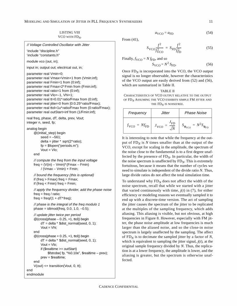
Recall that the PM jitter of FDM and FDN has already beenincluded as part of OSC, so the divider model incorporatedinto the VCO is noiseless and the jitter at the output of thenoiseless divider results only from the VCO jitter. Sincethe divider outputs one pulse for every N at its input, thevariance in the output period is the sum of the variance inN input periods. Thus, the jitter at the output is timeslarger than the jitter at the input, or
. (52)
Thus, to merge the divider into the VCO, the VCO gainmust be reduced by a factor of N, the jitter increased by afactor of , and the divider model removed.
After simulation, it is necessary to refer the computedresults, which are from the output of the divider, to the out-put of VCO, which is the true output of the PLL. Clearlythe jitter can be computed from (52).
To determine the affect of the divider on Sφ(ω), squareboth sides of (52) and apply (39)
. (53)
TVCO = TFD / N, and so
LISTING VIFIXED-FREQUENCY OSCILLATOR WITH FM AND PM JITTER.
// Fixed-Frequency Oscillator with Jitter
‘include “discipline.h”‘include “constants.h”
module osc (out);
output out; electrical out;
parameter real freq=1 from (0:inf);parameter real ratio=1 from (0:inf);parameter real Vlo=–1, Vhi=1;parameter real tt=0.01∗ratio/freq from (0:inf);parameter real fmJitter=0 from [0:0.1/freq);parameter real pmJitter=0 from [0:0.1∗ratio/freq);
integer n, fmSeed, pmSeed;real next, dT, dt, fmSD, pmSD;
analog begin@(initial_step) begin
fmSeed = 286;pmSeed = –459;fmSD = fmJitter∗sqrt(ratio/2);pmSD = pmJitter∗sqrt(0.5);next = 0.5/freq + $realtime;
end
@(timer(next + dt)) beginn = !n;dT = fmSD∗$dist_normal(fmSeed,0,1);dt = pmSD∗$dist_normal(pmSeed,0,1);next = next + 0.5∗ratio/freq + dT;
end
V(out) <+ transition(n ? Vhi : Vlo, 0, tt);endendmodule
LISTING VIIPFD/CP WITHOUT JITTER.
// Phase-Frequency Detector & Charge Pump
`include “discipline.h”`include “constants.h”
module pfd_cp (out, ref, vco);
input ref, vco; output out; electrical ref, vco, out;
parameter real Iout=100u;parameter integer dir=1 from [–1:1] exclude 0;
// dir = 1 for positive edge trigger// dir = –1 for negative edge trigger
parameter real tt=1n from (0:inf);parameter real ttol=1p from (0:inf);
integer state;
analog begin@(cross(V(ref), dir, ttol)) begin
if (state > –1) state = state – 1;end@(cross(V(vco), dir, ttol)) begin
if (state < 1) state = state + 1;end
I(out) <+ transition(Iout ∗ state, 0, tt);endendmodule
N
JFD NJVCO=
N
aVCOTVCO
aFDTFD
N-------------------=
MODELING AND SIMULATION OF JITTER IN PLL FREQUENCY SYNTHESIZERS 11
CADENCE CONFIDENTIAL
aVCO = aFD (54)
From (41),
(55)
Finally, fVCO = N fFD, and so
SVCO = N2 SFD. (56)
Once FDN is incorporated into the VCO, the VCO outputsignal is no longer observable, however the characteristicsof the VCO output are easily derived from (52) and (56),which are summarized in Table II.
It is interesting to note that while the frequency at the out-put of FDN is N times smaller than at the output of theVCO, except for scaling in the amplitude, the spectrum ofthe noise close to the fundamental is to a first degree unaf-fected by the presence of FDN. In particular, the width ofthe noise spectrum is unaffected by FDN. This is extremelyfortuitous, because it means that the number of cycles weneed to simulate is independent of the divide ratio N. Thus,large divide ratios do not affect the total simulation time.
To understand why FDN does not affect the width of thenoise spectrum, recall that while we started with a jitterthat varied continuously with time, j(t) in (7), for eitherefficiency or modeling reasons we eventually sampled it toend up with a discrete-time version. The act of samplingthe jitter causes the spectrum of the jitter to be replicatedat the multiples of the sampling frequency, which addsaliasing. This aliasing is visible, but not obvious, at highfrequencies in Figure 8. However, especially with FM jit-ter, the phase noise amplitude at low frequencies is muchlarger than the aliased noise, and so the close-in noisespectrum is largely unaffected by the sampling. The affectof FDN is to decimate the sampled jitter by a factor of N,which is equivalent to sampling the jitter signal, j(t), at theoriginal sample frequency divided by N. Thus, the replica-tion is at a lower frequency, the amplitude is lower, and thealiasing is greater, but the spectrum is otherwise unaf-fected.
LISTING VIIIVCO WITH FDN.
// Voltage Controlled Oscillator with Jitter
‘include “discipline.h”‘include “constants.h”
module vco (out, in);
input in; output out; electrical out, in;
parameter real Vmin=0;parameter real Vmax=Vmin+1 from (Vmin:inf);parameter real Fmin=1 from (0:inf);parameter real Fmax=2∗Fmin from (Fmin:inf);parameter real ratio=1 from (0:inf);parameter real Vlo=–1, Vhi=1;parameter real tt=0.01∗ratio/Fmax from (0:inf);parameter real jitter=0 from [0:0.25∗ratio/Fmax);parameter real ttol=1u∗ratio/Fmax from (0:ratio/Fmax);parameter real outStart=inf from (1/Fmin:inf);
real freq, phase, dT, delta, prev, Vout;integer n, seed, fp;
analog begin@(initial_step) begin
seed = –561;delta = jitter ∗ sqrt(2∗ratio);fp = $fopen(“periods.m”);Vout = Vlo;
end
// compute the freq from the input voltage freq = (V(in) – Vmin)∗(Fmax – Fmin)
/ (Vmax – Vmin) + Fmin;
// bound the frequency (this is optional)if (freq > Fmax) freq = Fmax;if (freq < Fmin) freq = Fmin;
// apply the frequency divider, add the phase noisefreq = freq / ratio;freq = freq/(1 + dT∗freq);
// phase is the integral of the freq modulo 1phase = idtmod(freq, 0.0, 1.0, –0.5);
// update jitter twice per period@(cross(phase – 0.25, +1, ttol)) begin
dT = delta ∗ $dist_normal(seed, 0, 1);Vout = Vhi;
end@(cross(phase + 0.25, +1, ttol)) begin
dT = delta ∗ $dist_normal(seed, 0, 1);Vout = Vlo;if ($realtime >= outStart)
$fstrobe( fp, “%0.10e”, $realtime – prev);prev = $realtime;
endV(out) <+ transition(Vout, 0, tt);
endendmodule
TABLE IICHARACTERISTICS OF VCO OUTPUT RELATIVE TO THE OUTPUT OF FDN ASSUMING THE VCO EXHIBITS SIMPLE FM JITTER AND
THE FDN IS NOISEFREE.
Frequency Jitter Phase Noise
SVCOf 2
fVCO2------------ SFD
f 2
fFD2--------=
fVCO NfFD= JVCO
JFD
N---------= SφVCO
N2SφFD=
12 KUNDERT
DRAFT
VII. CHARACTERIZING JITTER
The switching nature of the blocks in a PLL prevents useof the conventional noise analysis available from SPICE tocharacterize the noise of any of the blocks in a PLL withthe possible exception of the LF. The SPICE noise analysisoperates by linearizing the block about a DC operatingpoint, which is not sufficient when the block exhibitsswitching behavior. SpectreRF and the simulator devel-oped by Demir both linearize the circuit about a time-vary-ing operating point and compute the noise at the output ofthe block while taking into account both the effect of thetime-varying operating point on the bias-dependent noisesources and the time-varying nature of the transfer func-tion from the noise source to the output. They differ in thatSpectreRF is constrained to operate on periodic circuits. Inaddition, SpectreRF outputs noise as a function of fre-quency averaged over a period, while Demir’s simulatorcomputes the output noise as a function of time and inte-grated over all frequencies.
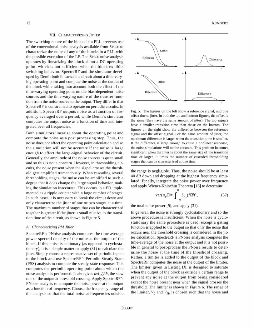
Both simulators linearize about the operating point andcompute the noise as a post processing step. Thus, thenoise does not affect the operating point calculation and sothe simulation will not be accurate if the noise is largeenough to affect the large-signal behavior of the circuit.Generally, the amplitude of the noise sources is quite smalland so this is not a concern. However, in thresholding cir-cuits, the noise present when the signal crosses the thresh-old gets amplified tremendously. When cascading severalthresholding stages, the noise can be amplified to such adegree that it does change the large signal behavior, mak-ing the simulation inaccurate. This occurs in a FD imple-mented as a ripple counter with a large number of stages.In such cases it is necessary to break the circuit down andonly characterize the jitter of one or two stages at a time.The maximum number of stages that can be characterizedtogether is greater if the jitter is small relative to the transi-tion time of the circuit, as shown in Figure 5.
A. Characterizing PM Jitter
SpectreRF’s PNoise analysis computes the time-averagepower spectral density of the noise at the output of theblock. If this noise is stationary (as opposed to cyclosta-tionary), it is a simple matter to apply (31) to calculate thejitter. Simply choose a representative set of periodic inputsto the block and use SpectreRF’s Periodic Steady State(PSS) analysis to compute the steady-state response. Thiscomputes the periodic operating point about which thenoise analysis is performed. It also gives dv(tc)/dt, the slewrate of the output at threshold crossing. Apply SpectreRF’sPNoise analysis to compute the noise power at the outputas a function of frequency. Choose the frequency range ofthe analysis so that the total noise at frequencies outside
the range is negligible. Thus, the noise should be at least40 dB down and dropping at the highest frequency simu-lated. Finally, integrate the noise power over frequencyand apply Wiener-Khinchin Theorem [16] to determine
, (57)
the total noise power [9], and apply (31).
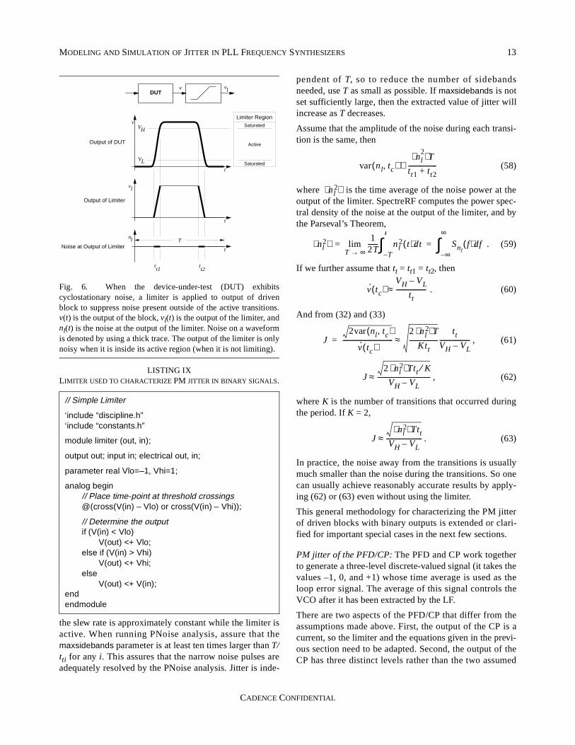
In general, the noise is strongly cyclostationary and so theabove procedure is insufficient. When the noise is cyclo-stationary the same procedure is used, except a gatingfunction is applied to the output so that only the noise thatoccurs near the threshold crossing is considered in the jit-ter calculation. SpectreRF’s PNoise analysis computes thetime-average of the noise at the output and it is not possi-ble in general to post-process the PNoise results to deter-mine the noise at the time of the threshold crossing.Rather, a limiter is added to the output of the block andSpectreRF computes the noise at the output of the limiter.The limiter, given in Listing IX, is designed to saturatewhen the output of the block is outside a certain range toprevent any noise at the output from being consideredexcept the noise present near when the signal crosses thethreshold. The limiter is shown in Figure 6. The range ofthe limiter, VL and VH, is chosen such that the noise and
Fig. 5. The figures on the left show a reference signal, and oneoffset due to jitter. In both the top and bottom figures, the offset isthe same (they have the same amount of jitter). The top signalshave a smaller transition time than those on the bottom. Thefigures on the right show the difference between the referencesignal and the offset signal. For the same amount of jitter, themaximum difference is larger when the transition time is smaller.If the difference is large enough to cause a nonlinear response,the noise simulations will not be accurate. This problem becomessignificant when the jitter is about the same size of the transitiontime or larger. It limits the number of cascaded thresholdingstages that can be characterized at one time.
Reference
Reference
Offset
Offset
Difference
Difference
v
v
v
v
tt
t t
var nv( ) Snvf( )df
∞–
∞
∫=
MODELING AND SIMULATION OF JITTER IN PLL FREQUENCY SYNTHESIZERS 13
CADENCE CONFIDENTIAL
the slew rate is approximately constant while the limiter isactive. When running PNoise analysis, assure that themaxsidebands parameter is at least ten times larger than T/tti for any i. This assures that the narrow noise pulses areadequately resolved by the PNoise analysis. Jitter is inde-
pendent of T, so to reduce the number of sidebandsneeded, use T as small as possible. If maxsidebands is notset sufficiently large, then the extracted value of jitter willincrease as T decreases.
Assume that the amplitude of the noise during each transi-tion is the same, then
(58)
where is the time average of the noise power at theoutput of the limiter. SpectreRF computes the power spec-tral density of the noise at the output of the limiter, and bythe Parseval’s Theorem,
. (59)
If we further assume that tt = tt1 = tt2, then
. (60)
And from (32) and (33)
, (61)
, (62)
where K is the number of transitions that occurred duringthe period. If K = 2,
. (63)
In practice, the noise away from the transitions is usuallymuch smaller than the noise during the transitions. So onecan usually achieve reasonably accurate results by apply-ing (62) or (63) even without using the limiter.
This general methodology for characterizing the PM jitterof driven blocks with binary outputs is extended or clari-fied for important special cases in the next few sections.
PM jitter of the PFD/CP: The PFD and CP work togetherto generate a three-level discrete-valued signal (it takes thevalues –1, 0, and +1) whose time average is used as theloop error signal. The average of this signal controls theVCO after it has been extracted by the LF.
There are two aspects of the PFD/CP that differ from theassumptions made above. First, the output of the CP is acurrent, so the limiter and the equations given in the previ-ous section need to be adapted. Second, the output of theCP has three distinct levels rather than the two assumed
Fig. 6. When the device-under-test (DUT) exhibitscyclostationary noise, a limiter is applied to output of drivenblock to suppress noise present outside of the active transitions.v(t) is the output of the block, vl(t) is the output of the limiter, andnl(t) is the noise at the output of the limiter. Noise on a waveformis denoted by using a thick trace. The output of the limiter is onlynoisy when it is inside its active region (when it is not limiting).
LISTING IXLIMITER USED TO CHARACTERIZE PM JITTER IN BINARY SIGNALS.
// Simple Limiter
‘include “discipline.h”‘include “constants.h”
module limiter (out, in);
output out; input in; electrical out, in;
parameter real Vlo=–1, Vhi=1;
analog begin// Place time-point at threshold crossings@(cross(V(in) – Vlo) or cross(V(in) – Vhi));
// Determine the outputif (V(in) < Vlo)
V(out) <+ Vlo;else if (V(in) > Vhi)
V(out) <+ Vhi;else
V(out) <+ V(in);endendmodule
t
vHV
LV
v lvDUT
Saturated
Active
Saturated
Limiter Region
Output of DUT
T
tt1
tt2
t
t
ln
lv
Output of Limiter
Noise at Output of Limiter
var nl tc,( )nl
2⟨ ⟩T
tt1 tt2+------------------≅
nl2⟨ ⟩
nl2⟨ ⟩
12T------ nl
2 t( )dtT–
T
∫T ∞→lim Snl
f( )df∞–
∞
∫= =
v· tc( )VH VL–
tt-------------------≈
J2var nl tc,( )
v· tc( )--------------------------------
2 nl2⟨ ⟩ T
Ktt------------------
ttVH VL–-------------------≈=
J2 nl
2⟨ ⟩ Ttt K⁄VH VL–
----------------------------------≈
Jnl
2⟨ ⟩ TttVH VL–-----------------------≈
14 KUNDERT
DRAFT
above. Thus, the CP has a ternary output rather than abinary output.
If it is necessary to apply a gating function, care must betaken because of the ternary nature of the output. A simplelimiter would allow the noise associated with the middlevalue to pass. So the simple limiter should be replacedwith a dead-band limiter. This is a limiter with a dead bandin the center of its input range. The dead band rejects noiseabout the equilibrium point associated with the middle ofthe three values.
PM Jitter of a FD: With ripple counters, one can onlycharacterize a few stages at a time because of the issueshown in Figure 5. Thus, a long ripple counter chain has tobe broken into smaller chains, and characterized individu-ally. The total jitter for the ripple counter is then computedby taking the square-root of the sum of the square of thejitter on each stage.
Unlike in ripple counters, jitter does not accumulate withsynchronous counters. Jitter in a synchronous counter isindependent of the number of stages. Rather, jitter of asynchronous counter is the jitter of its clock along with thejitter of the last stage.
The input to counters are generally edge sensitive, and soare only affected by jitter on either the positive-going orthe negative-going clock transitions, but not both. How-ever, this should not affect the way in which blocks arecharacterized as long as the behavioral models for thedividers also have edge-sensitive inputs. Then the behav-ioral model of the dividers only react to jitter on the properedge and ignore jitter on the other edge.
B. Characterizing FM Jitter
The noise of a free-running oscillator is dominated byphase noise, which is a random shifting of the frequency,and hence the phase, of the oscillation signal over time.The phase of an oscillator is subject to this variationbecause it is free running: there is no drive signal withwhich to lock and so no synchronization between the sig-nals generated by the oscillator and any reference signal.
Oscillator phase noise and FM jitter are different ways ofdescribing the same underlying phenomenon, and so thereis a direct conversion between phase noise and FM jitter,as given in (39). There is no need to invoke the use ofthresholds or gating functions in order to make the conver-sion.
VIII. SIMULATION AND ANALYSIS
The synthesizer is simulated using the netlist from ListingXI and the Verilog-A descriptions in Listings VI-VIII,modifying them as necessary to fit the actual circuit. The
simulation should cover an interval long enough to allowaccurate Fourier analysis at the lowest frequency of inter-est (Fmin). With deterministic signals, it is sufficient tosimulate for K cycles after the PLL settles if Fmin = 1/TK.However, for these signals, which are stochastic, it is bestto simulate for 10K to 100K cycles to allow for enoughaveraging to reduce the uncertainty in the result.
One should not simply apply an FFT to the output signalof the VCO/FDN to determine L(fm) for the PLL. Theresult would be quite inaccurate because the FFT samplesthe waveform at evenly spaced points, and so misses thejitter of the transitions. Instead, L(fm) can be measuredwith Spectre’s Fourier Analyzer, which uses a uniquealgorithm that does accurately resolve the jitter [12]. How-ever, it is slow if many frequencies are needed and so isnot well suited to this application.
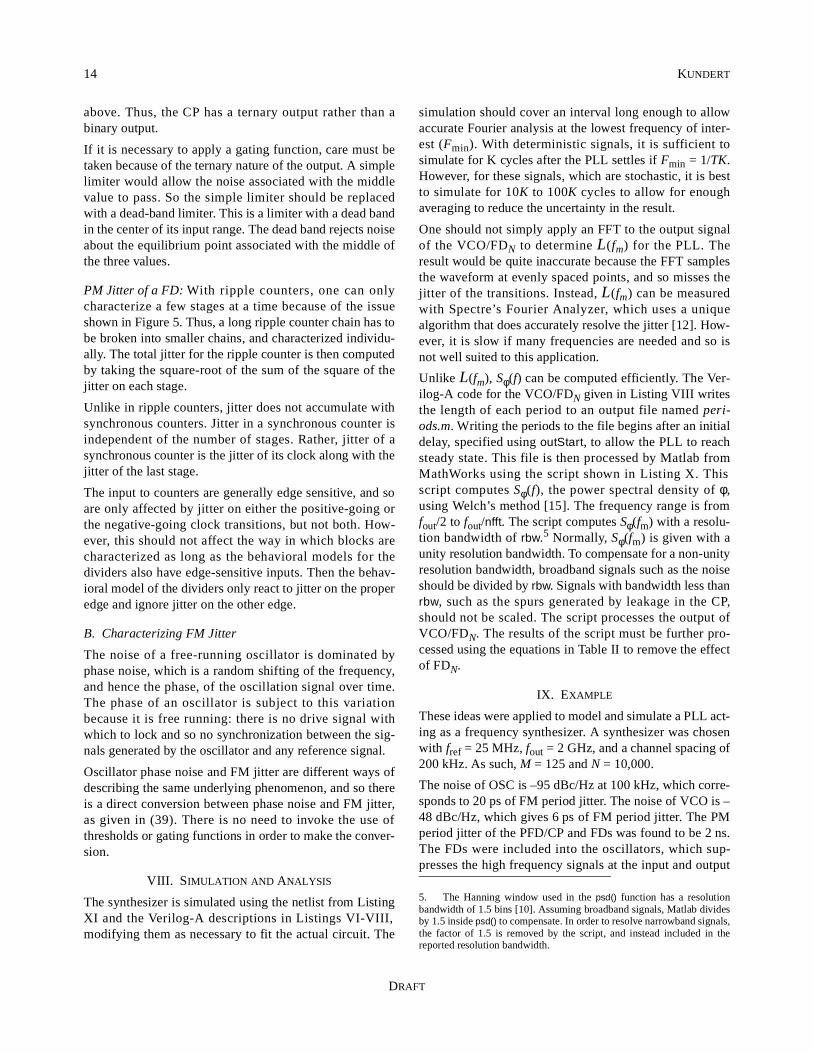
Unlike L(fm), Sφ(f) can be computed efficiently. The Ver-ilog-A code for the VCO/FDN given in Listing VIII writesthe length of each period to an output file named peri-ods.m. Writing the periods to the file begins after an initialdelay, specified using outStart, to allow the PLL to reachsteady state. This file is then processed by Matlab fromMathWorks using the script shown in Listing X. Thisscript computes Sφ(f), the power spectral density of φ,using Welch’s method [15]. The frequency range is fromfout/2 to fout/nfft. The script computes Sφ(fm) with a resolu-tion bandwidth of rbw.5 Normally, Sφ(fm) is given with aunity resolution bandwidth. To compensate for a non-unityresolution bandwidth, broadband signals such as the noiseshould be divided by rbw. Signals with bandwidth less thanrbw, such as the spurs generated by leakage in the CP,should not be scaled. The script processes the output ofVCO/FDN. The results of the script must be further pro-cessed using the equations in Table II to remove the effectof FDN.
IX. EXAMPLE
These ideas were applied to model and simulate a PLL act-ing as a frequency synthesizer. A synthesizer was chosenwith fref = 25 MHz, fout = 2 GHz, and a channel spacing of200 kHz. As such, M = 125 and N = 10,000.
The noise of OSC is –95 dBc/Hz at 100 kHz, which corre-sponds to 20 ps of FM period jitter. The noise of VCO is –48 dBc/Hz, which gives 6 ps of FM period jitter. The PMperiod jitter of the PFD/CP and FDs was found to be 2 ns.The FDs were included into the oscillators, which sup-presses the high frequency signals at the input and output
5. The Hanning window used in the psd() function has a resolutionbandwidth of 1.5 bins [10]. Assuming broadband signals, Matlab dividesby 1.5 inside psd() to compensate. In order to resolve narrowband signals,the factor of 1.5 is removed by the script, and instead included in thereported resolution bandwidth.
MODELING AND SIMULATION OF JITTER IN PLL FREQUENCY SYNTHESIZERS 15
CADENCE CONFIDENTIAL
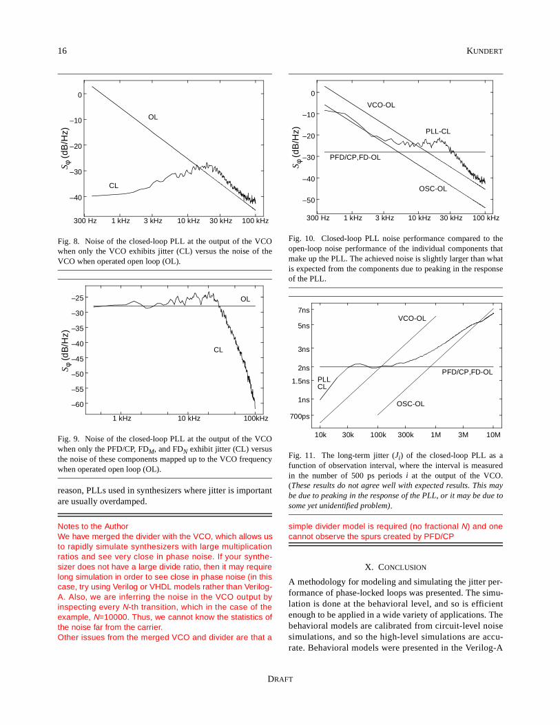
of the synthesizer. The netlist is shown in Listing XI. Theresults (compensated for non-unity resolution bandwidth(–28 dB) and for the suppression of the dividers (80 dB))are shown in Figures 7-10. The simulation took 7.5 min-utes for 450k time-points on a HP 9000/735. The use of alarge number of timepoints was motivated by the desire toreduce the level of uncertainty in the results. The periodjitter in the PLL was found to be 9.8 ps at the output of theVCO. The long-term jitter is shown in Figure 11.
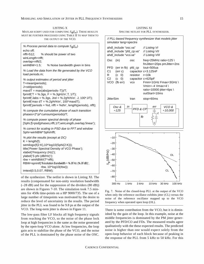
The low-pass filter LF blocks all high frequency signalsfrom reaching the VCO, so the noise of the phase lockloop at high frequencies is the same as the noise generatedby the open-loop VCO alone. At low frequencies, the loopgain acts to stabilize the phase of the VCO, and the noiseof the PLL is dominated by the phase noise of the OSC.
There is some contribution from the VCO, but it is dimin-ished by the gain of the loop. In this example, noise at themiddle frequencies is dominated by the PM jitter gener-ated by the PFD/CO and FDs. The measured results agreequalitatively with the these expected results. The predictednoise is higher than one would expect solely from theopen-loop behavior of each block because of peaking inthe response of the PLL from 5 kHz to 50 kHz. For this
LISTING XMATLAB SCRIPT USED FOR COMPUTING Sφ(fm). THESE RESULTS
MUST BE FURTHER PROCESSED USING TABLE II TO MAP THEM TO THE OUTPUT OF THE VCO.
% Process period data to compute Sφ(fm)echo off;nfft=512; % should be power of twowinLength=nfft;overlap=nfft/2;winNBW=1.5; % Noise bandwidth given in bins
% Load the data from the file generated by the VCOload periods.m;
% output estimates of period and jitterT=mean(periods);J=std(periods);maxdT = max(abs(periods–T))/T;fprintf(‘T = %.3gs, F = %.3gHz\n’,T, 1/T);fprintf(‘Jabs = %.3gs, Jrel = %.2g%%\n’, J, 100∗J/T);fprintf(‘max dT = %.2g%%\n’, 100∗maxdT);fprintf(‘periods = %d, nfft = %d\n’, length(periods), nfft);
% compute the cumulative phase of each transitionphases=2∗pi∗cumsum(periods)/T;
% compute power spectral density of phase[Sphi,f]=psd(phases,nfft,1/T,winLength,overlap,’linear’);
% correct for scaling in PSD due to FFT and windowSphi=winNBW∗Sphi/nfft;
% plot the results (except at DC)K = length(f);semilogx(f(2:K),10∗log10(Sphi(2:K)));title(‘Power Spectral Density of VCO Phase’);xlabel(‘Frequency (Hz)’);ylabel(‘S phi (dB/Hz)’);rbw = winNBW/(T∗nfft);RBW=sprintf(‘Resolution Bandwidth = %.0f Hz (%.0f dB)’,
rbw, 10∗log10(rbw));imtext(0.5,0.07, RBW);
LISTING XISPECTRE NETLIST FOR PLL SYNTHESIZER.
// PLL-based frequency synthesizer that models jittersimulator lang=spectre
ahdl_include “osc.va” // Listing VIahdl_include “pfd_cp.va” // Listing VIIahdl_include “vco.va” // Listing VIII
Osc (in) osc freq=25MHz ratio=125 \fmJitter=20ps pmJitter=2ns
PFD (err in fb) pfd_cp Iout=500uaC1 (err c) capacitor c=3.125nFR (c 0) resistor r=10kC2 (c 0) capacitor c=625pFVCO (fb err) vco Fmin=1GHz Fmax=3GHz \
Vmin=–4 Vmax=4 \ratio=10000 jitter=6ps \outStart=10ms
JitterSim tran stop=60ms
Fig. 7. Noise of the closed-loop PLL at the output of the VCOwhen only the reference oscillator exhibits jitter (CL) versus thenoise of the reference oscillator mapped up to the VCOfrequency when operated open loop (OL).
Osc &÷125
VCO &÷10,000PFD & CP
err
cfb
in
–80
–70
–60
–50
–40
–30
–20
–10
300 Hz 1 kHz 3 kHz 10 kHz 30 kHz 100 kHz
S φ (
dB/H
z)
OL
CL
16 KUNDERT
DRAFT
reason, PLLs used in synthesizers where jitter is importantare usually overdamped.
Notes to the AuthorWe have merged the divider with the VCO, which allows usto rapidly simulate synthesizers with large multiplicationratios and see very close in phase noise. If your synthe-sizer does not have a large divide ratio, then it may requirelong simulation in order to see close in phase noise (in thiscase, try using Verilog or VHDL models rather than Verilog-A. Also, we are inferring the noise in the VCO output byinspecting every N-th transition, which in the case of theexample, N=10000. Thus, we cannot know the statistics ofthe noise far from the carrier. Other issues from the merged VCO and divider are that a
simple divider model is required (no fractional N) and onecannot observe the spurs created by PFD/CP
X. CONCLUSION
A methodology for modeling and simulating the jitter per-formance of phase-locked loops was presented. The simu-lation is done at the behavioral level, and so is efficientenough to be applied in a wide variety of applications. Thebehavioral models are calibrated from circuit-level noisesimulations, and so the high-level simulations are accu-rate. Behavioral models were presented in the Verilog-A
Fig. 8. Noise of the closed-loop PLL at the output of the VCOwhen only the VCO exhibits jitter (CL) versus the noise of theVCO when operated open loop (OL).
Fig. 9. Noise of the closed-loop PLL at the output of the VCOwhen only the PFD/CP, FDM, and FDN exhibit jitter (CL) versusthe noise of these components mapped up to the VCO frequencywhen operated open loop (OL).
–40
–30
–20
–10
0
300 Hz 1 kHz 3 kHz 10 kHz 30 kHz 100 kHz
S φ (
dB/H
z)
OL
CL
–60
–55
–50
–45
–40
–35
–30
–25
1 kHz 10 kHz 100kHz
S φ (
dB
/Hz)
CL
OL
Fig. 10. Closed-loop PLL noise performance compared to theopen-loop noise performance of the individual components thatmake up the PLL. The achieved noise is slightly larger than whatis expected from the components due to peaking in the responseof the PLL.
Fig. 11. The long-term jitter (Ji) of the closed-loop PLL as afunction of observation interval, where the interval is measuredin the number of 500 ps periods i at the output of the VCO.(These results do not agree well with expected results. This maybe due to peaking in the response of the PLL, or it may be due tosome yet unidentified problem).
–50
–40
–30
–20
–10
0
300 Hz 1 kHz 3 kHz 10 kHz 30 kHz 100 kHz
S φ (
dB/H
z)
VCO-OL
OSC-OL
PFD/CP,FD-OL
PLL-CL
700ps
1ns
1.5ns
2ns
3ns
5ns
7ns
10k 30k 100k 300k 1M 3M 10M
PFD/CP,FD-OL
OSC-OL
VCO-OL
PLLCL
MODELING AND SIMULATION OF JITTER IN PLL FREQUENCY SYNTHESIZERS 17
CADENCE CONFIDENTIAL
language, however these same ideas can be used todevelop behavioral models in purely event-driven lan-guages such as Verilog-HDL and VHDL.
This methodology is flexible enough to be used in a broadrange of applications where jitter is important. Examplesinclude, clock generation and recovery, sampling systems,over-sampled ADCs, digital modulation and demodulationsystems, and fractional-N frequency synthesis (though it isnot possible to merge the VCO and divider in this case).
ACKNOWLEDGMENTS
I would like to thank Alper Demir and Manolis Terrovitisof the University of California in Berkeley for manyenlightening conversations about noise and jitter. I wouldalso like to thank Mark Chapman, Masayuki Takahashi,and Kimihiro Ogawa of Sony Semiconductor and RichDavis, Frank Hellmich and Randeep Soin of CadenceDesign Systems for their probing questions and insightfulcomments, as well as their help in validating these ideason real frequency synthesizers.
REFERENCES [1] H. Chang, E. Charbon, U. Choudhury, A. Demir, E. Felt, E.
Liu, E. Malavasi, A. Sangiovanni-Vincentelli, and I. Vassil-iou. A Top-Down Constraint-Driven Methodology for Ana-log Integrated Circuits. Kluwer Academic Publishers,1997.
[2] A. Demir, E. Liu, A. Sangiovanni-Vincentelli, and I. Vas-siliou. Behavioral simulation techniques for phase/delay-locked systems. Proceedings of the IEEE Custom Integrat-ed Circuits Conference, pp. 453-456, May 1994.
[3] A. Demir, E. Liu, and A. Sangiovanni-Vincentelli. Time-domain non-Monte-Carlo noise simulation for nonlineardynamic circuits with arbitrary excitations. IEEE Transac-tions on Computer-Aided Design of Integrated Circuits andSystems, vol. 15, no. 5, pp. 493-505, May 1996.
[4] A. Demir, A. Sangiovanni-Vincentelli. Simulation andmodeling of phase noise in open-loop oscillators. Proceed-ings of the IEEE Custom Integrated Circuits Conference,pp. 445-456, May 1996.
[5] A. Demir, A. Sangiovanni-Vincentelli. Analysis and Simu-lation of Noise in Nonlinear Electronic Circuits and Sys-tems. Kluwer Academic Publishers, 1997.
[6] A. Demir, A. Mehrotra, J. Roychowdhury. Phase noise inoscillators: a unifying theory and numerical methods forcharacterization. Proceedings of the 35th Design Automa-tion Conference, June 1998.
[7] D. FitzPatrick, I. Miller. Analog Behavioral Modeling withthe Verilog-A Language. Kluwer Academic Publishers,1997.
[8] F. Gardner. Phaselock Techniques. John Wiley & Sons,1979.
[9] W. Gardner. Introduction to Random Processes: With Ap-plications to Signals and Systems. McGraw-Hill, 1989.
[10] F. Harris. On the use of windows for harmonic analysis withthe discrete Fourier transform. Proceedings of the IEEE,vol. 66, no. 1, January 1978.
[11] P. R. Gray and R. G. Meyer. Analysis and Design of AnalogIntegrated Circuits. J. Wiley & Sons, Third Edition, 1993.
[12] K. Kundert. The Designer’s Guide to SPICE and Spectre.Kluwer Academic Publishers, 1995.
[13] J. McNeill. Jitter in Ring Oscillators. IEEE Journal of Sol-id-State Circuits, vol. 32, no. 6, June 1997.
[14] Verilog-A Language Reference Manual: Analog Extensionsto Verilog-HDL, version 1.0. Open Verilog International,1996. Available from www.ovi.org.
[15] A. Oppenheim, R. Schafer. Digital Signal Processing.Prentice-Hall, 1975.
[16] A. Papoulis. Probability, Random Variables, and Stochas-tic Processes. McGraw-Hill, 1991.
[17] R. Telichevesky, K. Kundert, J. White. Receiver character-ization using periodic small-signal analysis. Proceedings ofthe IEEE Custom Integrated Circuits Conference, May1996.
[18] R. Telichevesky, K. Kundert, J. White. Efficient AC andnoise analysis of two-tone RF circuits. Proceedings of the33rd Design Automation Conference, June 1996.
[19] G. Vendelin, A. Pavio, U. Rohde. Microwave Circuit De-sign. J. Wiley & Sons, 1990.
STILL TO DO
1. Include flicker noise from oscillator.
2. Model nonlinear dependence of VCO noise, amplitude,and frequency to the control signal.
3. Generate small-signal noise model of PLL for use inPNoise analysis (includes correlations).
4. Describe how to model dead-zone in PFD/CP.
5. Describe how to see the spurs created by the PFD/CP(keep the frequency divider in the circuit; if the divideratio is very large, consider partitioning it into two factorsand make one explicit and the other implicit).

Cadence Design Systems, Inc.
Corporate Headquarters2655 Seely AvenueSan Jose, CA 95134800.746.6223408.943.1234www.cadence.com
© 2001 Cadence Design Systems, Inc. All rights reserved. Cadence and the Cadence logo areregistered trademarks and “how big can you dream?” is a trademark of Cadence DesignSystems, Inc. All others are properties of their holders.
Stock #3487 10/01