model no.: m185bge suffix: l23
TRANSCRIPT
PRODUCT SPECIFICATION
Version 1.0 15.Jun.2011 1 /28
The copyright belongs to CHIMEI InnoLux. Any unauthorized use is prohibited.
Customer: APPROVED BY SIGNATURE Name / Title Note Product Version B1 Please return 1 copy for your confirmation with your signature and comments.
Doc. Number :
Tentative Specification Preliminary Specification Approval Specification
MODEL NO.: M185BGE SUFFIX: L23
Approved By Checked By Prepared By
PRODUCT SPECIFICATION
Version 1.0 15.Jun.2011 2 /28
The copyright belongs to CHIMEI InnoLux. Any unauthorized use is prohibited.
CONTENTS
1. GENERAL DESCRIPTION ......................................................................................................5 1.1 OVERVIEW........................................................................................................................5 1.2 GENERAL SPECIFICATIONS ...........................................................................................5
2. MECHANICAL SPECIFICATIONS...........................................................................................5 3. ABSOLUTE MAXIMUM RATINGS ..........................................................................................6
3.1 ABSOLUTE RATINGS OF ENVIRONMENT......................................................................6 3.2 ELECTRICAL ABSOLUTE RATINGS ................................................................................6
3.2.1 TFT LCD MODULE .................................................................................................... 6 3.2.2 BACKLIGHT UNIT...................................................................................................... 7
4. ELECTRICAL SPECIFICATIONS............................................................................................7 4.1 FUNCTION BLOCK DIAGRAM..........................................................................................7 4.2. INTERFACE CONNECTIONS ..........................................................................................8 4.3 ELECTRICAL CHARACTERISTICS ................................................................................10
4.3.1 LCD ELETRONICS SPECIFICATION ...................................................................... 10 4.3.2 Vcc Power Dip Condition.......................................................................................... 12 4.3.3 BACKLIGHT UNIT.................................................................................................... 12 4.4.3 LIGHTBAR Connector Pin Assignment .................................................................... 13
4.4 LVDS INPUT SIGNAL SPECIFICATIONS........................................................................14 4.4.1 LVDS DATA MAPPING TABLE ................................................................................. 14 4.4.2 COLOR DATA INPUT ASSIGNMENT....................................................................... 14
4.5 DISPLAY TIMING SPECIFICATIONS ..............................................................................15 4.6 POWER ON/OFF SEQUENCE........................................................................................17
5. OPTICAL CHARACTERISTICS ............................................................................................18 5.1 TEST CONDITIONS ........................................................................................................18 5.2 OPTICAL SPECIFICATIONS ...........................................................................................18
6. RELIABILITY TEST ITEM......................................................................................................21 7. PACKING ...............................................................................................................................22
7.1 PACKING SPECIFICATIONS ..........................................................................................22 7.2 PACKING METHOD.........................................................................................................22 7.3 PALLET............................................................................................................................23
8. CMI MODULE LABEL ...........................................................................................................24 9. PRECAUTIONS .....................................................................................................................25
9.1 ASSEMBLY AND HANDLING PRECAUTIONS................................................................25 9.2 STORAGE PRECAUTIONS.............................................................................................25 9.3 OPERATION PRECAUTIONS .........................................................................................25
PRODUCT SPECIFICATION
Version 1.0 15.Jun.2011 3 /28
The copyright belongs to CHIMEI InnoLux. Any unauthorized use is prohibited.
9.4 SAFETY PRECAUTIONS ................................................................................................26 9.5 SAFETY STANDARDS ....................................................................................................26 9.6 OTHER ............................................................................................................................26
Appendix. OUTLINE DRAWING ...............................................................................................26
PRODUCT SPECIFICATION
Version 1.0 15.Jun.2011 4 /28
The copyright belongs to CHIMEI InnoLux. Any unauthorized use is prohibited.
REVISION HISTORY
Version Date Page Description
1.0 16.Jun, 2011 All Spec Ver.1.0 was first issued.
PRODUCT SPECIFICATION
Version 1.0 15.Jun.2011 5 /28
The copyright belongs to CHIMEI InnoLux. Any unauthorized use is prohibited.
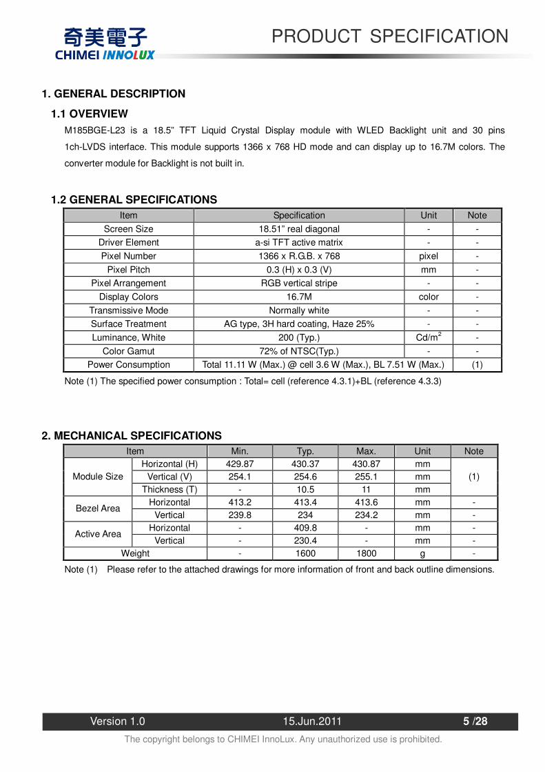
1. GENERAL DESCRIPTION
1.1 OVERVIEW M185BGE-L23 is a 18.5” TFT Liquid Crystal Display module with WLED Backlight unit and 30 pins
1ch-LVDS interface. This module supports 1366 x 768 HD mode and can display up to 16.7M colors. The
converter module for Backlight is not built in.
1.2 GENERAL SPECIFICATIONS Item Specification Unit Note
Screen Size 18.51” real diagonal - - Driver Element a-si TFT active matrix - - Pixel Number 1366 x R.G.B. x 768 pixel -
Pixel Pitch 0.3 (H) x 0.3 (V) mm - Pixel Arrangement RGB vertical stripe - -
Display Colors 16.7M color - Transmissive Mode Normally white - - Surface Treatment AG type, 3H hard coating, Haze 25% - - Luminance, White 200 (Typ.) Cd/m2 -
Color Gamut 72% of NTSC(Typ.) - - Power Consumption Total 11.11 W (Max.) @ cell 3.6 W (Max.), BL 7.51 W (Max.) (1)
Note (1) The specified power consumption : Total= cell (reference 4.3.1)+BL (reference 4.3.3)
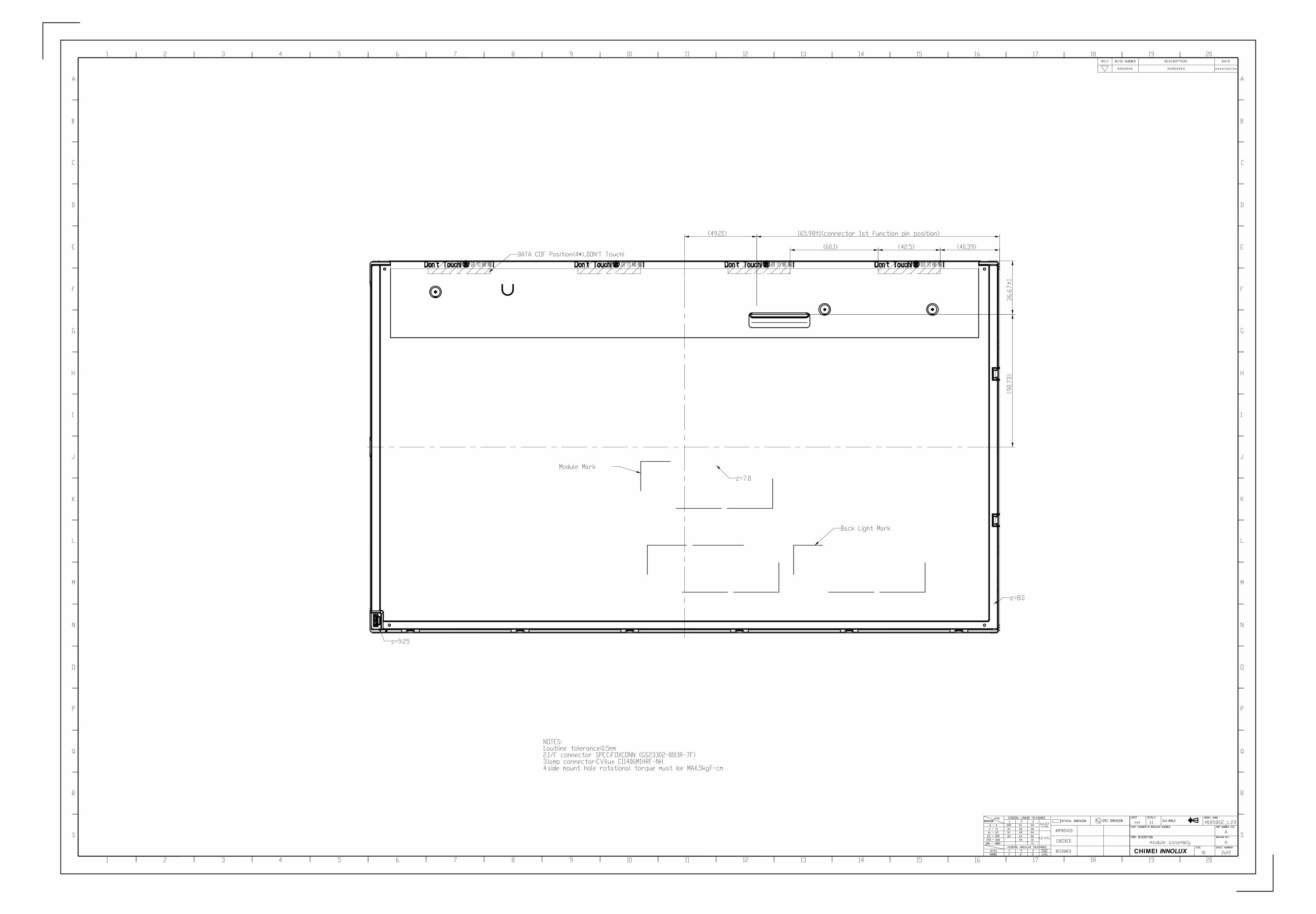
2. MECHANICAL SPECIFICATIONS Item Min. Typ. Max. Unit Note
Horizontal (H) 429.87 430.37 430.87 mm Vertical (V) 254.1 254.6 255.1 mm Module Size
Thickness (T) - 10.5 11 mm (1)
Horizontal 413.2 413.4 413.6 mm - Bezel Area
Vertical 239.8 234 234.2 mm - Horizontal - 409.8 - mm -
Active Area Vertical - 230.4 - mm -
Weight - 1600 1800 g -
Note (1) Please refer to the attached drawings for more information of front and back outline dimensions.
PRODUCT SPECIFICATION
Version 1.0 15.Jun.2011 6 /28
The copyright belongs to CHIMEI InnoLux. Any unauthorized use is prohibited.
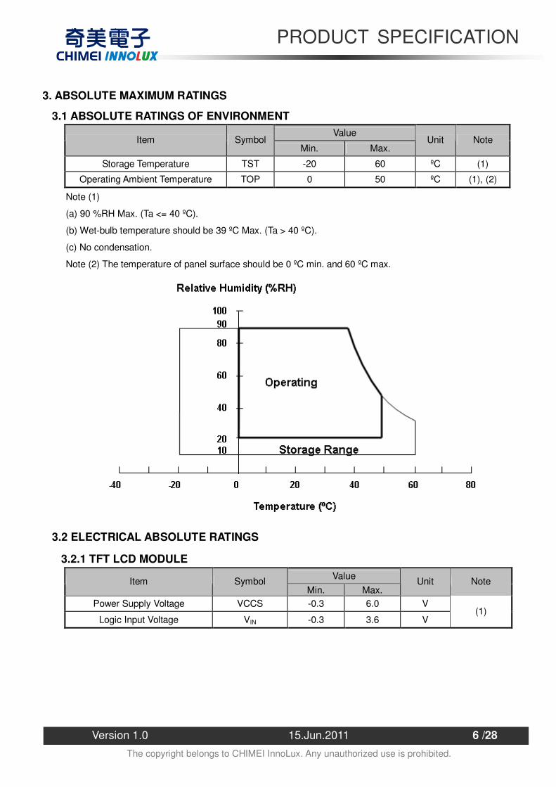
3. ABSOLUTE MAXIMUM RATINGS
3.1 ABSOLUTE RATINGS OF ENVIRONMENT Value
Item Symbol Min. Max.
Unit Note
Storage Temperature TST -20 60 ºC (1)
Operating Ambient Temperature TOP 0 50 ºC (1), (2)
Note (1)
(a) 90 %RH Max. (Ta <= 40 ºC).
(b) Wet-bulb temperature should be 39 ºC Max. (Ta > 40 ºC).
(c) No condensation.
Note (2) The temperature of panel surface should be 0 ºC min. and 60 ºC max.
3.2 ELECTRICAL ABSOLUTE RATINGS
3.2.1 TFT LCD MODULE Value Item Symbol
Min. Max. Unit Note
Power Supply Voltage VCCS -0.3 6.0 V
Logic Input Voltage VIN -0.3 3.6 V (1)
PRODUCT SPECIFICATION
Version 1.0 15.Jun.2011 7 /28
The copyright belongs to CHIMEI InnoLux. Any unauthorized use is prohibited.
3.2.2 BACKLIGHT UNIT Value Item Symbol
Min. Typ Max. Unit Note
LED Forward Current Per Input Pin IF 0 65 69 mA (1), (2)
Duty=100%
LED Pulse Forward Current Per Input Pin IP - - 150 mA
(1), (2) Pulse Width 10msec.
and Duty 10%
Note (1) Permanent damage to the device may occur if maximum values are exceeded. Function operation
should be restricted to the conditions described under Normal Operating Conditions.
Note (2) Specified values are for input pin of LED light bar at Ta=25±2 (Refer to 4.3.3 and 4.3.4 for
further information).
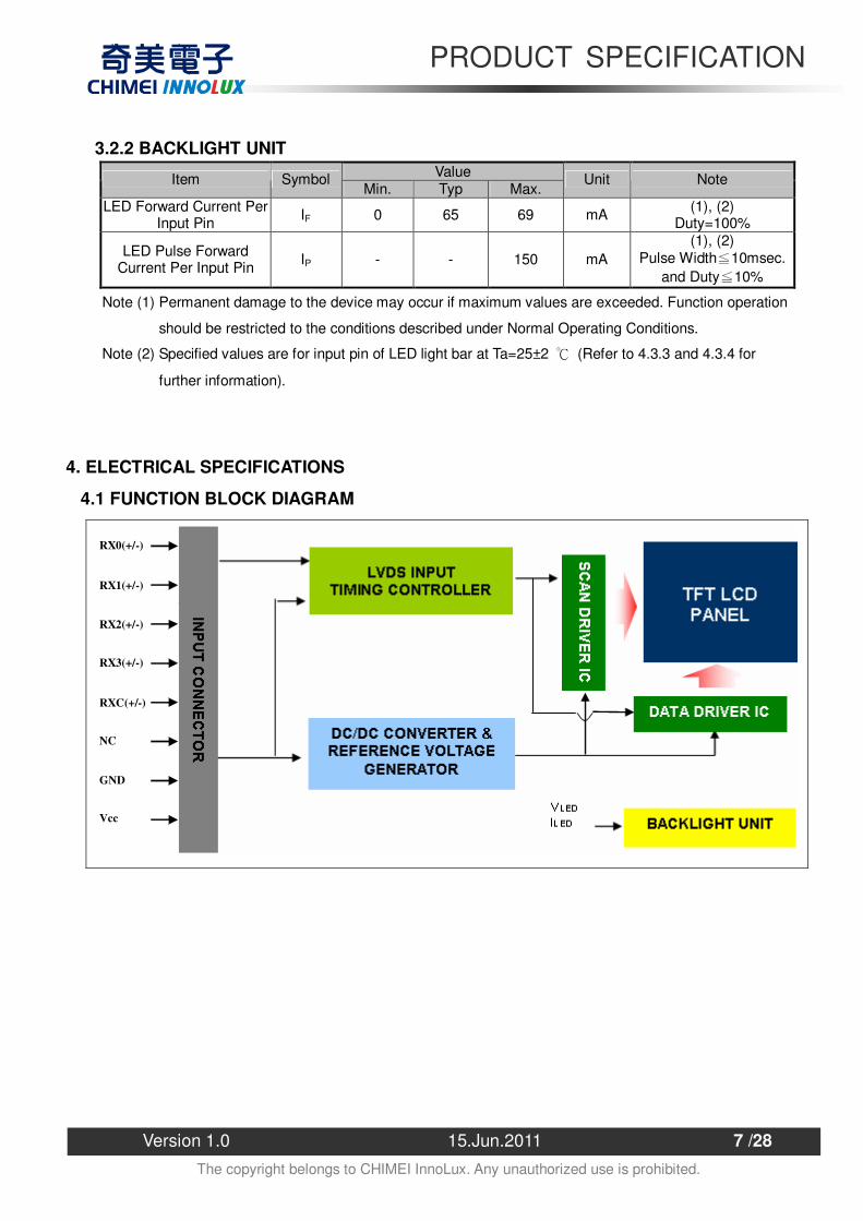
4. ELECTRICAL SPECIFICATIONS
4.1 FUNCTION BLOCK DIAGRAM
RX0(+/-)
RX1(+/-)
RX2(+/-)
RX3(+/-)
RXC(+/-)
NC
GND
Vcc
PRODUCT SPECIFICATION
Version 1.0 15.Jun.2011 8 /28
The copyright belongs to CHIMEI InnoLux. Any unauthorized use is prohibited.
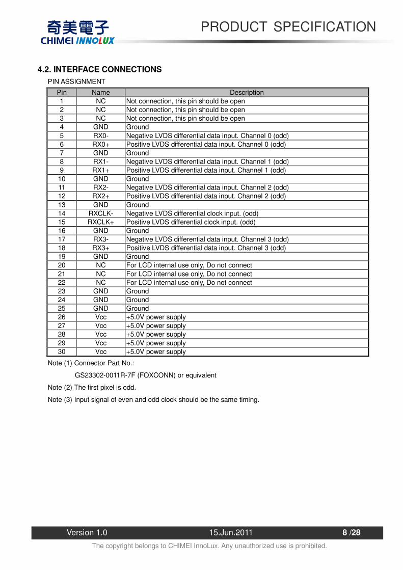
4.2. INTERFACE CONNECTIONS PIN ASSIGNMENT
Pin Name Description 1 NC Not connection, this pin should be open 2 NC Not connection, this pin should be open 3 NC Not connection, this pin should be open 4 GND Ground 5 RX0- Negative LVDS differential data input. Channel 0 (odd) 6 RX0+ Positive LVDS differential data input. Channel 0 (odd) 7 GND Ground 8 RX1- Negative LVDS differential data input. Channel 1 (odd) 9 RX1+ Positive LVDS differential data input. Channel 1 (odd)
10 GND Ground 11 RX2- Negative LVDS differential data input. Channel 2 (odd) 12 RX2+ Positive LVDS differential data input. Channel 2 (odd) 13 GND Ground 14 RXCLK- Negative LVDS differential clock input. (odd) 15 RXCLK+ Positive LVDS differential clock input. (odd) 16 GND Ground 17 RX3- Negative LVDS differential data input. Channel 3 (odd) 18 RX3+ Positive LVDS differential data input. Channel 3 (odd) 19 GND Ground 20 NC For LCD internal use only, Do not connect 21 NC For LCD internal use only, Do not connect 22 NC For LCD internal use only, Do not connect 23 GND Ground 24 GND Ground 25 GND Ground 26 Vcc +5.0V power supply 27 Vcc +5.0V power supply 28 Vcc +5.0V power supply 29 Vcc +5.0V power supply 30 Vcc +5.0V power supply
Note (1) Connector Part No.:
GS23302-0011R-7F (FOXCONN) or equivalent
Note (2) The first pixel is odd.
Note (3) Input signal of even and odd clock should be the same timing.

PRODUCT SPECIFICATION
Version 1.0 15.Jun.2011 9 /28
The copyright belongs to CHIMEI InnoLux. Any unauthorized use is prohibited.
1,1 (odd) 1,2
(even) 1,3 (odd) 1,4
(even) 2,1 2,2
3,1
Ymax,1 Ymax, Xmax
1,Xmax
Pitch
Pitch
PRODUCT SPECIFICATION
Version 1.0 15.Jun.2011 10 /28
The copyright belongs to CHIMEI InnoLux. Any unauthorized use is prohibited.
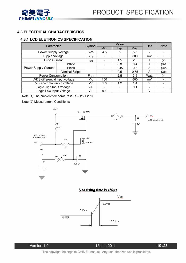
4.3 ELECTRICAL CHARACTERISTICS
4.3.1 LCD ELETRONICS SPECIFICATION Value Parameter Symbol
Min. Typ. Max. Unit Note
Power Supply Voltage Vcc 4.5 5 5.5 V - Ripple Voltage VRP - - 300 mV - Rush Current IRUSH - 1.5 2.0 A (2)
White - 0.3 0.4 A (3)a Black - 0.45 0.6 A (3)b Power Supply Current
Vertical Stripe
- 0.5 0.65 A (3)c Power Consumption PLCD - 2.5 3.6 Watt (4)
LVDS differential input voltage Vid 100 - 600 mV - LVDS common input voltage Vic 1.0 1.2 1.4 V -
Logic High Input Voltage VIH - - 0.1 V - Logic Low Input Voltage VIL 0.1 - - V -
Note (1) The ambient temperature is Ta = 25 ± 2 ºC.
Note (2) Measurement Conditions:
PRODUCT SPECIFICATION
Version 1.0 15.Jun.2011 11 /28
The copyright belongs to CHIMEI InnoLux. Any unauthorized use is prohibited.
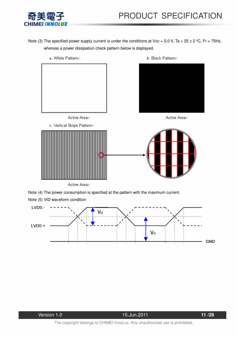
Note (3) The specified power supply current is under the conditions at Vcc = 5.0 V, Ta = 25 ± 2 ºC, Fr = 75Hz,
whereas a power dissipation check pattern below is displayed.
Note (4) The power consumption is specified at the pattern with the maximum current.
Note (5) VID waveform condition

PRODUCT SPECIFICATION
Version 1.0 15.Jun.2011 12 /28
The copyright belongs to CHIMEI InnoLux. Any unauthorized use is prohibited.
4.3.2 Vcc Power Dip Condition
4.3.3 BACKLIGHT UNIT Value Parameter Symbol
Min. Typ. Max. Unit Note
LED Light Bar Input Voltage Per Input Pin VPIN - 24.8 27.2 V
(1), Duty=100%, IPIN=65mA
LED Light Bar Current Per Input Pin IPIN - 65 69 mA (1), (2)
Duty=100% LED Life Time LLED 40000 - - Hrs (3)
Power Consumption PBL - 6.45 7.51 W (1)
Duty=100%, IPIN=65mA
Note (1) LED light bar input voltage and current are measured by utilizing a true RMS multimeter as shown
below:
Note (2) PBL(Typ) = IPIN(Typ) VPIN(Typ) ( 4 ), PBL(Max) = IPIN(Max) VPIN(Max) ( 4 ) input pins.
Note (3) The lifetime of LED is defined as the time when LED packages continue to operate under the
conditions at Ta = 25 ±2 and I= (65)mA (per chip) until the brightness becomes 50% of its
original value.
PRODUCT SPECIFICATION
Version 1.0 15.Jun.2011 13 /28
The copyright belongs to CHIMEI InnoLux. Any unauthorized use is prohibited.
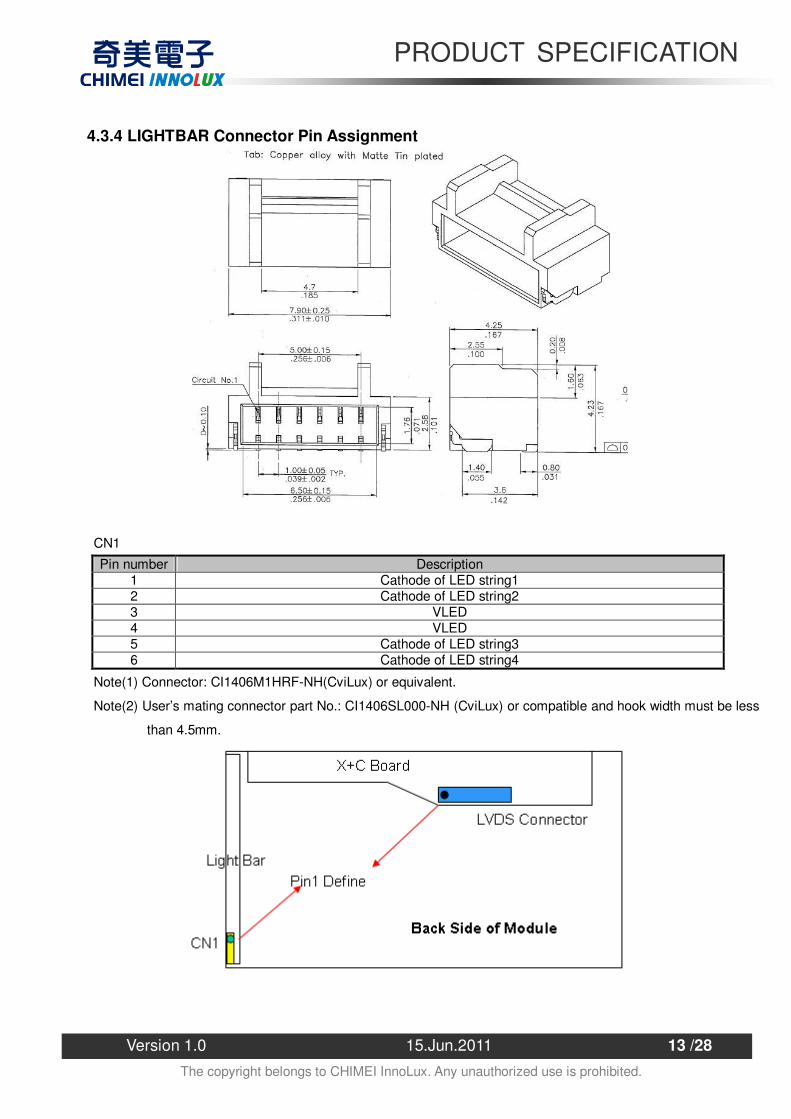
4.3.4 LIGHTBAR Connector Pin Assignment
CN1
Pin number Description 1 Cathode of LED string1 2 Cathode of LED string2 3 VLED 4 VLED 5 Cathode of LED string3 6 Cathode of LED string4
Note(1) Connector: CI1406M1HRF-NH(CviLux) or equivalent.
Note(2) User’s mating connector part No.: CI1406SL000-NH (CviLux) or compatible and hook width must be less
than 4.5mm.
PRODUCT SPECIFICATION
Version 1.0 15.Jun.2011 14 /28
The copyright belongs to CHIMEI InnoLux. Any unauthorized use is prohibited.
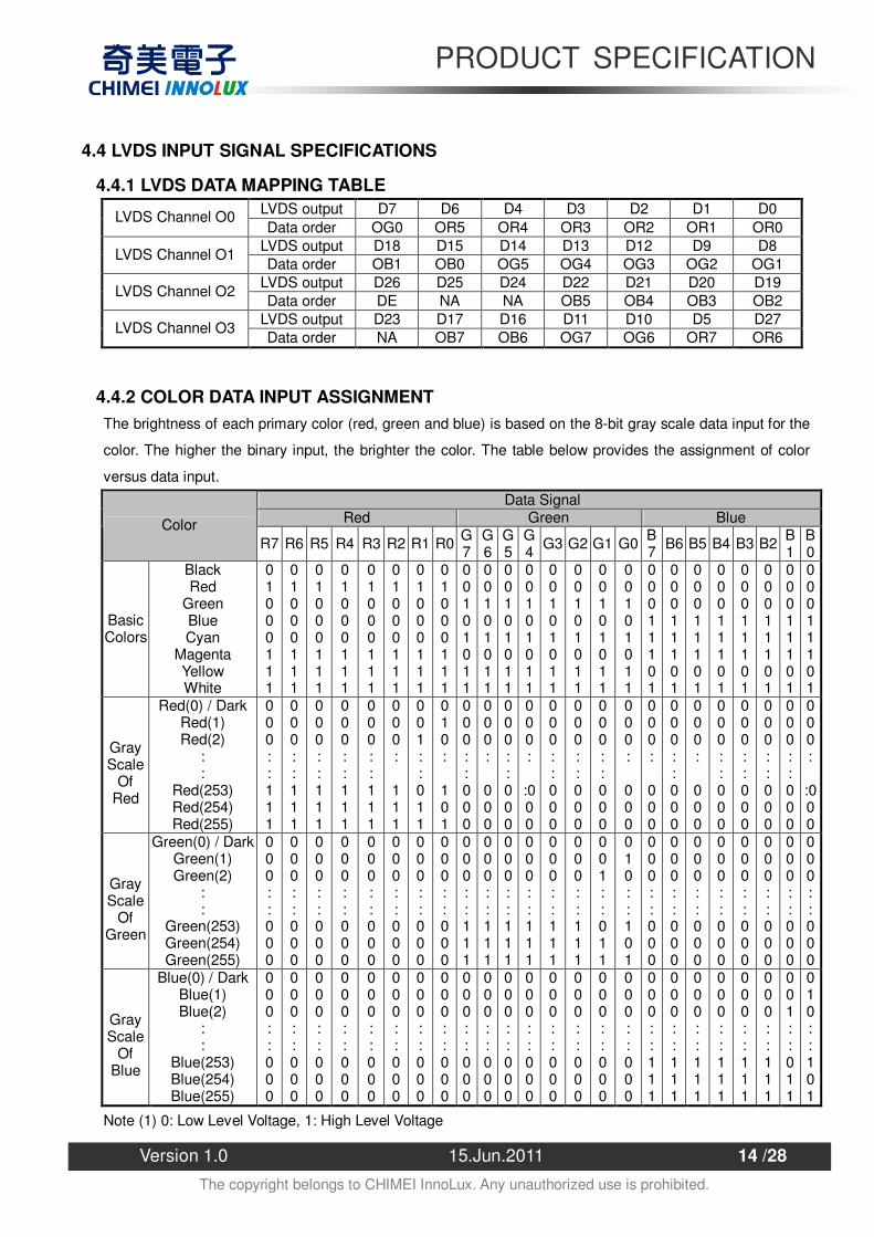
4.4 LVDS INPUT SIGNAL SPECIFICATIONS
4.4.1 LVDS DATA MAPPING TABLE LVDS output D7 D6 D4 D3 D2 D1 D0 LVDS Channel O0 Data order OG0 OR5 OR4 OR3 OR2 OR1 OR0
LVDS output D18 D15 D14 D13 D12 D9 D8 LVDS Channel O1 Data order OB1 OB0 OG5 OG4 OG3 OG2 OG1
LVDS output D26 D25 D24 D22 D21 D20 D19 LVDS Channel O2 Data order DE NA NA OB5 OB4 OB3 OB2
LVDS output D23 D17 D16 D11 D10 D5 D27 LVDS Channel O3 Data order NA OB7 OB6 OG7 OG6 OR7 OR6
4.4.2 COLOR DATA INPUT ASSIGNMENT The brightness of each primary color (red, green and blue) is based on the 8-bit gray scale data input for the
color. The higher the binary input, the brighter the color. The table below provides the assignment of color
versus data input.
Data Signal Red Green Blue Color
R7 R6 R5 R4 R3 R2 R1 R0 G7
G6
G5
G4 G3 G2 G1 G0 B
7 B6 B5 B4 B3 B2 B1
B0
Basic Colors
Black Red
Green Blue Cyan
Magenta Yellow White
0 1 0 0 0 1 1 1
0 1 0 0 0 1 1 1
0 1 0 0 0 1 1 1
0 1 0 0 0 1 1 1
0 1 0 0 0 1 1 1
0 1 0 0 0 1 1 1
0 1 0 0 0 1 1 1
0 1 0 0 0 1 1 1
0 0 1 0 1 0 1 1
0 0 1 0 1 0 1 1
0 0 1 0 1 0 1 1
0 0 1 0 1 0 1 1
0 0 1 0 1 0 1 1
0 0 1 0 1 0 1 1
0 0 1 0 1 0 1 1
0 0 1 0 1 0 1 1
0 0 0 1 1 1 0 1
0 0 0 1 1 1 0 1
0 0 0 1 1 1 0 1
0 0 0 1 1 1 0 1
0 0 0 1 1 1 0 1
0 0 0 1 1 1 0 1
0 0 0 1 1 1 0 1
0 0 0 1 1 1 0 1
Gray Scale
Of Red
Red(0) / Dark Red(1) Red(2)
: :
Red(253) Red(254) Red(255)
0 0 0 : : 1 1 1
0 0 0 : : 1 1 1
0 0 0 : : 1 1 1
0 0 0 : : 1 1 1
0 0 0 : : 1 1 1
0 0 0 :
1 1 1
0 0 1 : : 0 1 1
0 1 0 :
1 0 1
0 0 0 : : 0 0 0
0 0 0 :
0 0 0
0 0 0 : : 0 0 0
0 0 0 :
:0 0 0
0 0 0 : : 0 0 0
0 0 0 : : 0 0 0
0 0 0 : : 0 0 0
0 0 0 :
0 0 0
0 0 0 :
0 0 0
0 0 0 : : 0 0 0
0 0 0 :
0 0 0
0 0 0 : : 0 0 0
0 0 0 : : 0 0 0
0 0 0 : : 0 0 0
0 0 0 : : 0 0 0
0 0 0 :
:0 0 0
Gray Scale
Of Green
Green(0) / Dark Green(1) Green(2)
: :
Green(253) Green(254) Green(255)
0 0 0 : : 0 0 0
0 0 0 : : 0 0 0
0 0 0 : : 0 0 0
0 0 0 : : 0 0 0
0 0 0 : : 0 0 0
0 0 0 : : 0 0 0
0 0 0 : : 0 0 0
0 0 0 : : 0 0 0
0 0 0 : : 1 1 1
0 0 0 : : 1 1 1
0 0 0 : : 1 1 1
0 0 0 : : 1 1 1
0 0 0 : : 1 1 1
0 0 0 : : 1 1 1
0 0 1 : : 0 1 1
0 1 0 : : 1 0 1
0 0 0 : : 0 0 0
0 0 0 : : 0 0 0
0 0 0 : : 0 0 0
0 0 0 : : 0 0 0
0 0 0 : : 0 0 0
0 0 0 : : 0 0 0
0 0 0 : : 0 0 0
0 0 0 : : 0 0 0
Gray Scale
Of Blue
Blue(0) / Dark Blue(1) Blue(2)
: :
Blue(253) Blue(254) Blue(255)
0 0 0 : : 0 0 0
0 0 0 : : 0 0 0
0 0 0 : : 0 0 0
0 0 0 : : 0 0 0
0 0 0 : : 0 0 0
0 0 0 : : 0 0 0
0 0 0 : : 0 0 0
0 0 0 : : 0 0 0
0 0 0 : : 0 0 0
0 0 0 : : 0 0 0
0 0 0 : : 0 0 0
0 0 0 : : 0 0 0
0 0 0 : : 0 0 0
0 0 0 : : 0 0 0
0 0 0 : : 0 0 0
0 0 0 : : 0 0 0
0 0 0 : : 1 1 1
0 0 0 : : 1 1 1
0 0 0 : : 1 1 1
0 0 0 : : 1 1 1
0 0 0 : : 1 1 1
0 0 0 : : 1 1 1
0 0 1 : : 0 1 1
0 1 0 : : 1 0 1
Note (1) 0: Low Level Voltage, 1: High Level Voltage
PRODUCT SPECIFICATION
Version 1.0 15.Jun.2011 15 /28
The copyright belongs to CHIMEI InnoLux. Any unauthorized use is prohibited.
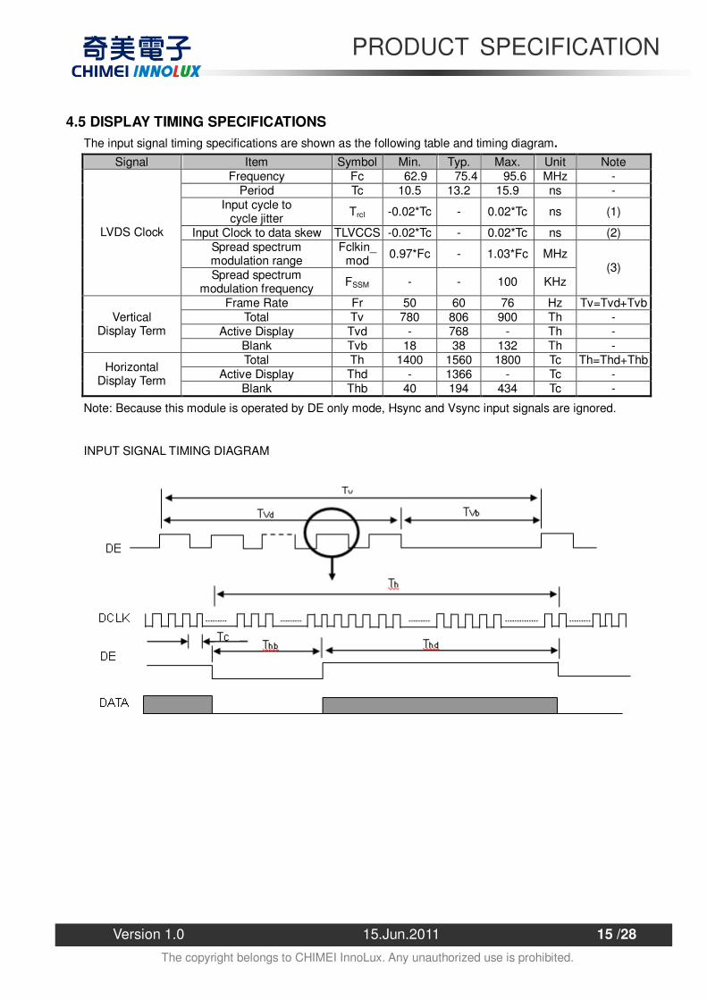
4.5 DISPLAY TIMING SPECIFICATIONS The input signal timing specifications are shown as the following table and timing diagram.
Signal Item Symbol Min. Typ. Max. Unit Note Frequency Fc 62.9 75.4 95.6 MHz -
Period Tc 10.5 13.2 15.9 ns - Input cycle to
cycle jitter Trcl -0.02*Tc - 0.02*Tc ns (1)
Input Clock to data skew TLVCCS -0.02*Tc - 0.02*Tc ns (2) Spread spectrum modulation range
Fclkin_mod
0.97*Fc - 1.03*Fc MHz
LVDS Clock
Spread spectrum modulation frequency FSSM - - 100 KHz
(3)
Frame Rate Fr 50 60 76 Hz Tv=Tvd+Tvb Total Tv 780 806 900 Th -
Active Display Tvd - 768 - Th - Vertical
Display Term Blank Tvb 18 38 132 Th - Total Th 1400 1560 1800 Tc Th=Thd+Thb
Active Display Thd - 1366 - Tc - Horizontal Display Term
Blank Thb 40 194 434 Tc -
Note: Because this module is operated by DE only mode, Hsync and Vsync input signals are ignored.
INPUT SIGNAL TIMING DIAGRAM
PRODUCT SPECIFICATION
Version 1.0 15.Jun.2011 16 /28
The copyright belongs to CHIMEI InnoLux. Any unauthorized use is prohibited.
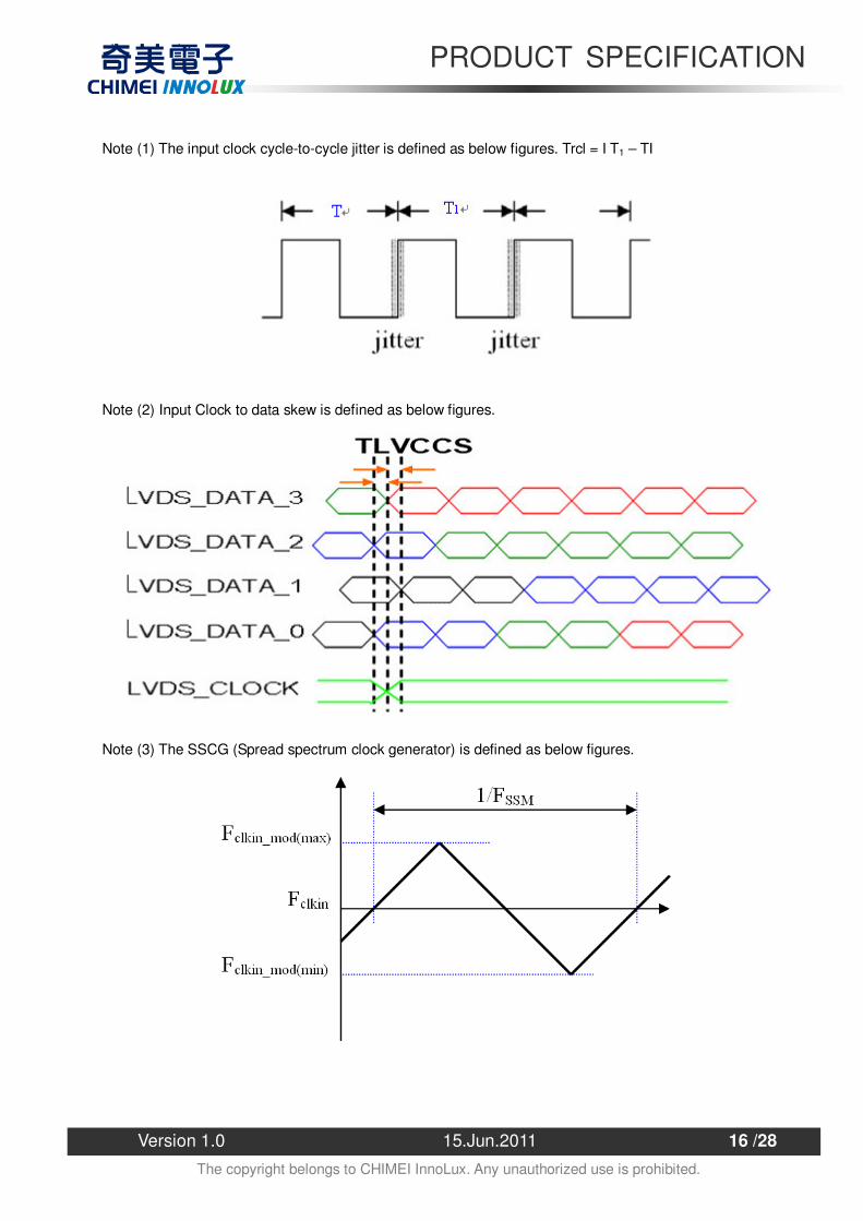
Note (1) The input clock cycle-to-cycle jitter is defined as below figures. Trcl = I T1 – TI
Note (2) Input Clock to data skew is defined as below figures.
Note (3) The SSCG (Spread spectrum clock generator) is defined as below figures.
PRODUCT SPECIFICATION
Version 1.0 15.Jun.2011 17 /28
The copyright belongs to CHIMEI InnoLux. Any unauthorized use is prohibited.
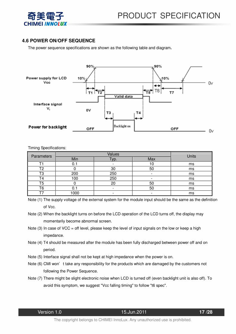
4.6 POWER ON/OFF SEQUENCE The power sequence specifications are shown as the following table and diagram.
Timing Specifications:
Values Parameters Min Typ. Max
Units
T1 0.1 - 10 ms T2 0 30 50 ms T3 200 250 - ms T4 100 250 - ms T5 0 20 50 ms T6 0.1 - 50 ms T7 1000 - - ms
Note (1) The supply voltage of the external system for the module input should be the same as the definition
of Vcc.
Note (2) When the backlight turns on before the LCD operation of the LCD turns off, the display may
momentarily become abnormal screen.
Note (3) In case of VCC = off level, please keep the level of input signals on the low or keep a high
impedance.
Note (4) T4 should be measured after the module has been fully discharged between power off and on
period.
Note (5) Interface signal shall not be kept at high impedance when the power is on.
Note (6) CMI won t take any responsibility for the products which are damaged by the customers not
following the Power Sequence.
Note (7) There might be slight electronic noise when LCD is turned off (even backlight unit is also off). To
avoid this symptom, we suggest "Vcc falling timing" to follow "t6 spec".

PRODUCT SPECIFICATION
Version 1.0 15.Jun.2011 18 /28
The copyright belongs to CHIMEI InnoLux. Any unauthorized use is prohibited.
5. OPTICAL CHARACTERISTICS
5.1 TEST CONDITIONS Item Symbol Value Unit
Ambient Temperature Ta 25�2 oC Ambient Humidity Ha 50�10 %RH
Supply Voltage VCC 5 V Input Signal According to typical value in "3. ELECTRICAL CHARACTERISTICS"
LED Light Bar Input Current Per Input Pin IPIN 65 ± 1.9 mADC
PWM Duty Ratio D 100 % LED Light Bar Test Converter TEST01001 T2-A1
5.2 OPTICAL SPECIFICATIONS The relative measurement methods of optical characteristics are shown in 5.2. The following items should be
measured under the test conditions described in 5.1 and stable environment shown in Note (5).
Item Symbol Condition Min. Typ. Max. Unit Note Rx 0.641
Red Ry 0.338
Gx 0.315 Green Gy 0.629 Bx 0.159
Blue By 0.059 Wx 0.313
Color Chromaticity (CIE 1931)
White Wy
Typ – 0.03
0.329
Typ + 0.03 - (1), (5)
Center Luminance of White (Center of Screen) LC 150 200 - cd/m2 (4), (5)
Contrast Ratio CR
�x=0�, �Y =0� CS-2000
R=G=B=255 Gray scale
500 700 - - (2), (5) TR - 1.5 2.5 Response Time TF �x=0�, �Y =0� - 3.5 5.5
ms (3)
White Variation W x=0, Y =0 75 - - % (5), (6) Horizontal �x- + �x+ 80 90 -
Viewing Angle Vertical �y- + �y+
CR 10 55 65 -
Deg. (1), (5)
Horizontal �x- + �x+ 100 110 - Viewing Angle
Vertical �y- + �y+ CR 5
75 85 - Deg. (1), (5)
PRODUCT SPECIFICATION
Version 1.0 15.Jun.2011 19 /28
The copyright belongs to CHIMEI InnoLux. Any unauthorized use is prohibited.
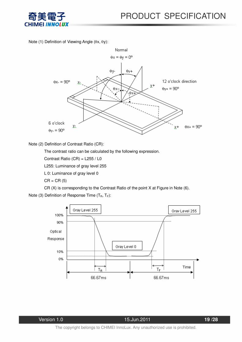
Note (1) Definition of Viewing Angle (�x, �y):
Note (2) Definition of Contrast Ratio (CR):
The contrast ratio can be calculated by the following expression.
Contrast Ratio (CR) = L255 / L0
L255: Luminance of gray level 255
L 0: Luminance of gray level 0
CR = CR (5)
CR (X) is corresponding to the Contrast Ratio of the point X at Figure in Note (6).
Note (3) Definition of Response Time (TR, TF):
PRODUCT SPECIFICATION
Version 1.0 15.Jun.2011 20 /28
The copyright belongs to CHIMEI InnoLux. Any unauthorized use is prohibited.
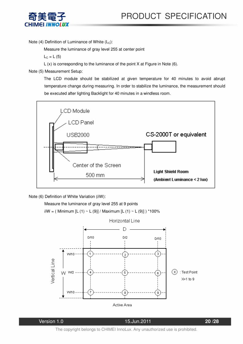
Note (4) Definition of Luminance of White (LC):
Measure the luminance of gray level 255 at center point
LC = L (5)
L (x) is corresponding to the luminance of the point X at Figure in Note (6).
Note (5) Measurement Setup:
The LCD module should be stabilized at given temperature for 40 minutes to avoid abrupt
temperature change during measuring. In order to stabilize the luminance, the measurement should
be executed after lighting Backlight for 40 minutes in a windless room.
Note (6) Definition of White Variation (�W):
Measure the luminance of gray level 255 at 9 points
�W = ( Minimum [L (1) ~ L (9)] / Maximum [L (1) ~ L (9)] ) *100%
PRODUCT SPECIFICATION
Version 1.0 15.Jun.2011 21 /28
The copyright belongs to CHIMEI InnoLux. Any unauthorized use is prohibited.
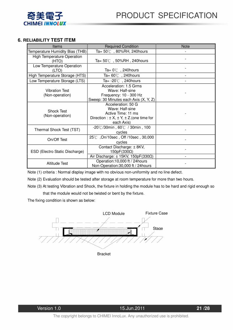
6. RELIABILITY TEST ITEM Items Required Condition Note
Temperature Humidity Bias (THB) Ta= 50 , 80%RH, 240hours - High Temperature Operation
(HTO) Ta= 50 , 50%RH , 240hours -
Low Temperature Operation (LTO) Ta= 0 , 240hours -
High Temperature Storage (HTS) Ta= 60 , 240hours - Low Temperature Storage (LTS) Ta= -20 , 240hours -
Vibration Test (Non-operation)
Acceleration: 1.5 Grms Wave: Half-sine
Frequency: 10 - 300 Hz Sweep: 30 Minutes each Axis (X, Y, Z)
-
Shock Test (Non-operation)
Acceleration: 50 G Wave: Half-sine
Active Time: 11 ms Direction : ± X, ± Y, ± Z.(one time for
each Axis)
-
Thermal Shock Test (TST) -20 /30min , 60 / 30min , 100 cycles
-
On/Off Test 25 ,On/10sec , Off /10sec , 30,000 cycles
-
Contact Discharge: ± 8KV, 150pF(330�) - ESD (Electro Static Discharge)
Air Discharge: ± 15KV, 150pF(330�) -
Altitude Test Operation:10,000 ft / 24hours Non-Operation:30,000 ft / 24hours -
Note (1) criteria : Normal display image with no obvious non-uniformity and no line defect.
Note (2) Evaluation should be tested after storage at room temperature for more than two hours.
Note (3) At testing Vibration and Shock, the fixture in holding the module has to be hard and rigid enough so
that the module would not be twisted or bent by the fixture.
The fixing condition is shown as below:
LCD Module Fixture Case
Stage
Bracket
PRODUCT SPECIFICATION
Version 1.0 15.Jun.2011 22 /28
The copyright belongs to CHIMEI InnoLux. Any unauthorized use is prohibited.
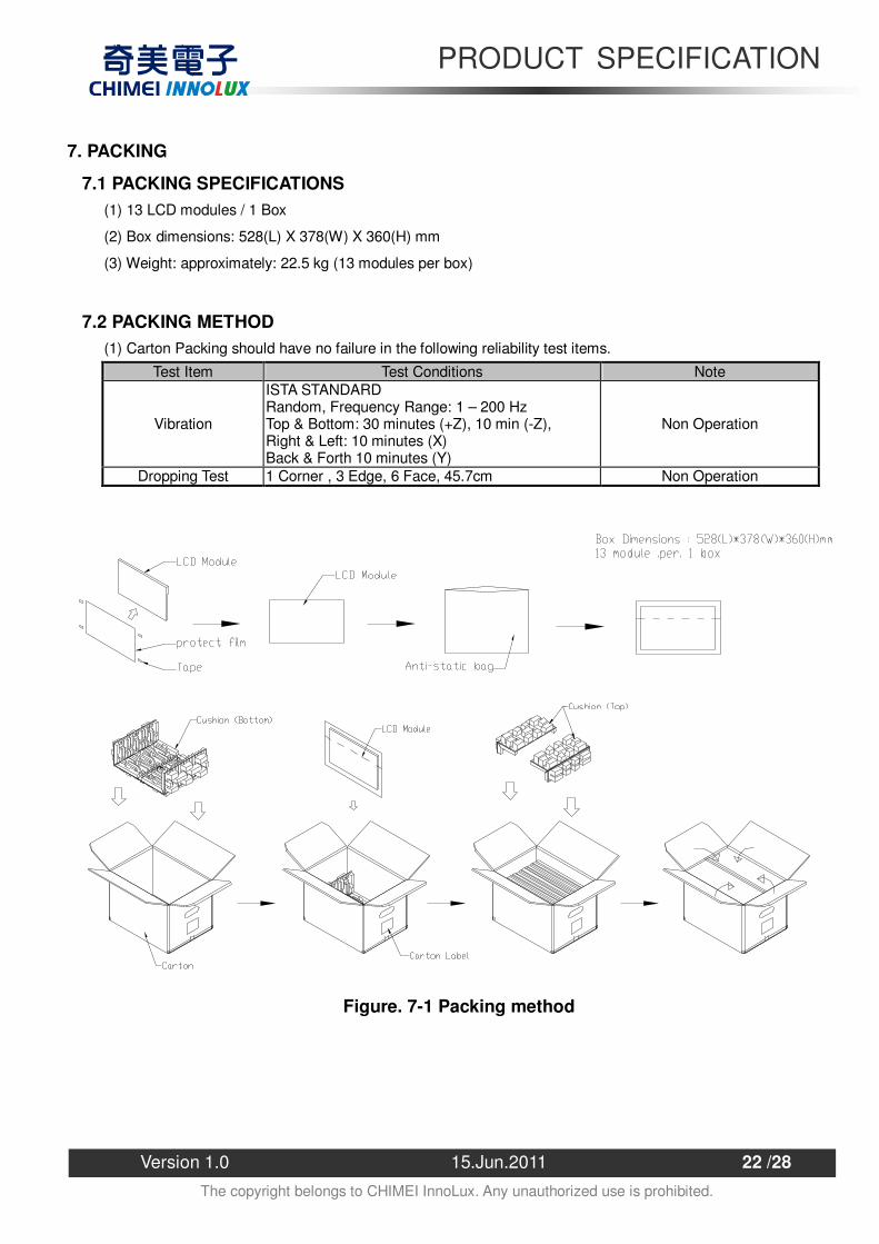
7. PACKING
7.1 PACKING SPECIFICATIONS (1) 13 LCD modules / 1 Box
(2) Box dimensions: 528(L) X 378(W) X 360(H) mm
(3) Weight: approximately: 22.5 kg (13 modules per box)
7.2 PACKING METHOD (1) Carton Packing should have no failure in the following reliability test items.
Test Item Test Conditions Note
Vibration
ISTA STANDARD Random, Frequency Range: 1 – 200 Hz Top & Bottom: 30 minutes (+Z), 10 min (-Z), Right & Left: 10 minutes (X) Back & Forth 10 minutes (Y)
Non Operation
Dropping Test 1 Corner , 3 Edge, 6 Face, 45.7cm Non Operation
Figure. 7-1 Packing method
PRODUCT SPECIFICATION
Version 1.0 15.Jun.2011 23 /28
The copyright belongs to CHIMEI InnoLux. Any unauthorized use is prohibited.
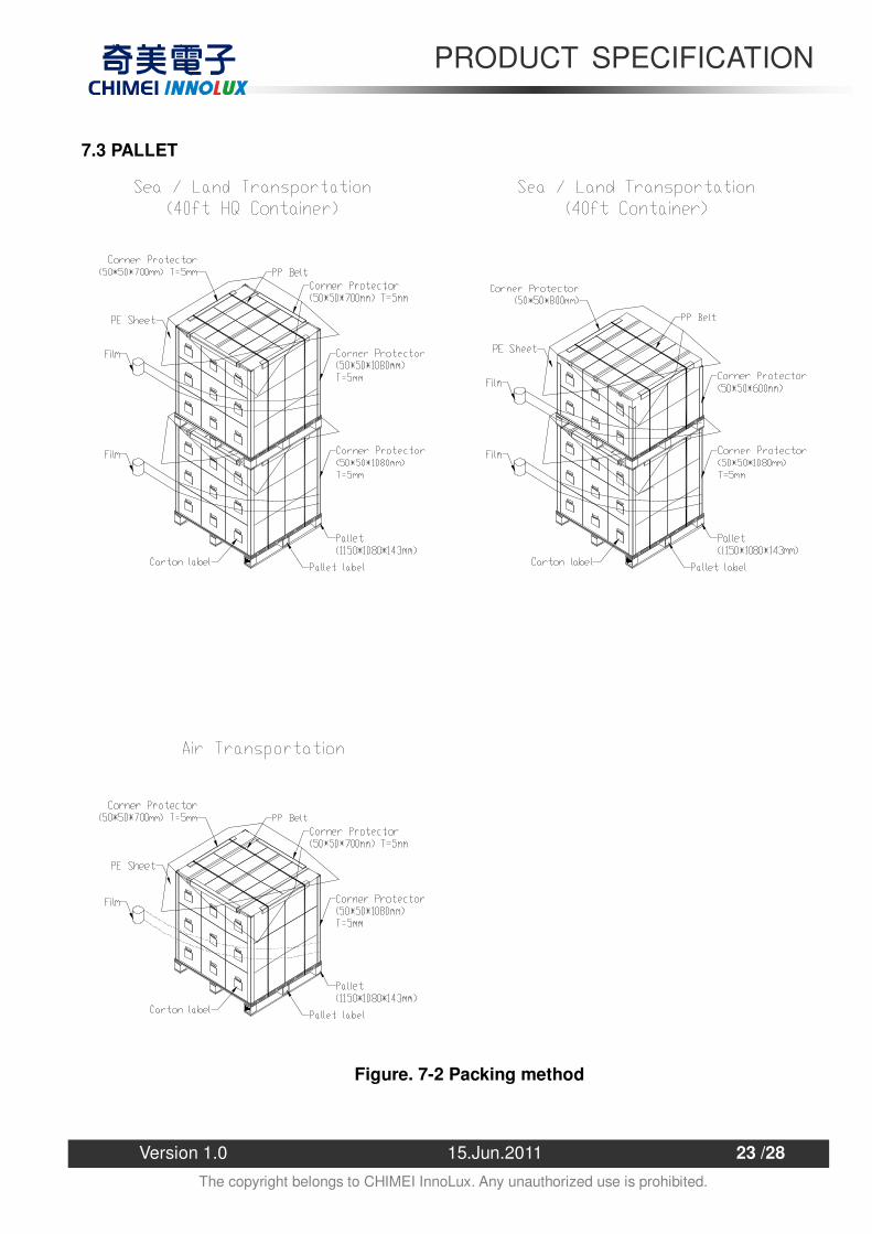
7.3 PALLET
Figure. 7-2 Packing method
PRODUCT SPECIFICATION
Version 1.0 15.Jun.2011 24 /28
The copyright belongs to CHIMEI InnoLux. Any unauthorized use is prohibited.
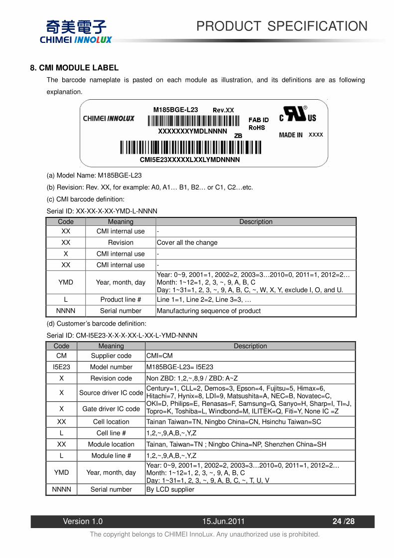
8. CMI MODULE LABEL The barcode nameplate is pasted on each module as illustration, and its definitions are as following
explanation.
(a) Model Name: M185BGE-L23
(b) Revision: Rev. XX, for example: A0, A1… B1, B2… or C1, C2…etc.
(c) CMI barcode definition:
Serial ID: XX-XX-X-XX-YMD-L-NNNN
Code Meaning Description XX CMI internal use -
XX Revision Cover all the change
X CMI internal use -
XX CMI internal use -
YMD Year, month, day Year: 0~9, 2001=1, 2002=2, 2003=3…2010=0, 2011=1, 2012=2… Month: 1~12=1, 2, 3, ~, 9, A, B, C Day: 1~31=1, 2, 3, ~, 9, A, B, C, ~, W, X, Y, exclude I, O, and U.
L Product line # Line 1=1, Line 2=2, Line 3=3, …
NNNN Serial number Manufacturing sequence of product
(d) Customer’s barcode definition:
Serial ID: CM-I5E23-X-X-X-XX-L-XX-L-YMD-NNNN
Code Meaning Description CM Supplier code CMI=CM
I5E23 Model number M185BGE-L23= I5E23
X Revision code Non ZBD: 1,2,~,8,9 / ZBD: A~Z
X Source driver IC code
X Gate driver IC code
Century=1, CLL=2, Demos=3, Epson=4, Fujitsu=5, Himax=6, Hitachi=7, Hynix=8, LDI=9, Matsushita=A, NEC=B, Novatec=C, OKI=D, Philips=E, Renasas=F, Samsung=G, Sanyo=H, Sharp=I, TI=J, Topro=K, Toshiba=L, Windbond=M, ILITEK=Q, Fiti=Y, None IC =Z
XX Cell location Tainan Taiwan=TN, Ningbo China=CN, Hsinchu Taiwan=SC
L Cell line # 1,2,~,9,A,B,~,Y,Z
XX Module location Tainan, Taiwan=TN ; Ningbo China=NP, Shenzhen China=SH
L Module line # 1,2,~,9,A,B,~,Y,Z
YMD Year, month, day Year: 0~9, 2001=1, 2002=2, 2003=3…2010=0, 2011=1, 2012=2… Month: 1~12=1, 2, 3, ~, 9, A, B, C Day: 1~31=1, 2, 3, ~, 9, A, B, C, ~, T, U, V
NNNN Serial number By LCD supplier
CMI5E23XXXXXLXXLYMDNNNN
XXXXXXXYMDLNNNN
M185BGE-L23
PRODUCT SPECIFICATION
Version 1.0 15.Jun.2011 25 /28
The copyright belongs to CHIMEI InnoLux. Any unauthorized use is prohibited.
(e) FAB ID(UL Factory ID):
Region Factory ID
TWCMI GEMN
NBCMI LEOO
NBCME CANO NHCMI CAPG
9. PRECAUTIONS
9.1 ASSEMBLY AND HANDLING PRECAUTIONS (1) Do not apply rough force such as bending or twisting to the module during assembly.
(2) To assemble or install module into user’s system can be only in clean working areas. The dust and oil
may cause electrical short or worsen the polarizer.
(3) It’s not permitted to have pressure or impulse on the module because the LCD panel and Backlight will
be damaged.
(4) Always follow the correct power sequence when LCD module is connecting and operating. This can
prevent damage to the CMOS LSI chips during latch-up.
(5) Do not pull the I/F connector in or out while the module is operating.
(6) Do not disassemble the module.
(7) Use a soft dry cloth without chemicals for cleaning, because the surface of polarizer is very soft and
easily scratched.
(8) It is dangerous that moisture come into or contacted the LCD module, because moisture may damage
LCD module when it is operating.
(9) High temperature or humidity may reduce the performance of module. Please store LCD module within
the specified storage conditions.
(10)When ambient temperature is lower than 10ºC may reduce the display quality. For example, the
response time will become slowly.
9.2 STORAGE PRECAUTIONS (1) Do not leave the module in high temperature, and high humidity for a long time. It is highly recommended
to store the module with temperature from 0 to 35 and relative humidity of less than 70%.
(2) Do not store the TFT – LCD module in direct sunlight.
(3) The module should be stored in dark place. It is prohibited to apply sunlight or fluorescent light in storing.
9.3 OPERATION PRECAUTIONS (1) The LCD product should be operated under normal condition.
Normal condition is defined as below :
Temperature : 20±15
Humidity: 65±20%
Display pattern : continually changing pattern(Not stationary)
PRODUCT SPECIFICATION
Version 1.0 15.Jun.2011 26 /28
The copyright belongs to CHIMEI InnoLux. Any unauthorized use is prohibited.
(2) If the product will be used in extreme conditions such as high temperature, high humidity, high
altitude ,display pattern or operation time etc…It is strongly recommended to contact CMI for application
engineering advice . Otherwise , Its reliability and function may not be guaranteed.
9.4 SAFETY PRECAUTIONS (1) If the liquid crystal material leaks from the panel, it should be kept away from the eyes or mouth. In case
of contact with hands, skin or clothes, it has to be washed away thoroughly with soap.
(2) After the module’s end of life, it is not harmful in case of normal operation and storage.
9.5 SAFETY STANDARDS The LCD module should be certified with safety regulations as follows:
(1) UL60950-1 or updated standard.
(2) IEC60950-1 or updated standard.
9.6 OTHER When fixed patterns are displayed for a long time, remnant image is likely to occur.
Appendix. OUTLINE DRAWING Refer to next 2 pages.