model answer - pimpri chinchwad polytechnic...figure. the figures drawn by candidate and model...
TRANSCRIPT
MAHARASHTRA STATE BOARD OF TECHNICAL EDUCATION
(Autonomous)
(ISO/IEC - 27001 - 2005 Certified)
MODEL ANSWER
SUMMER - 2017 EXAMINATION
Subject: Advanced Microprocessor Subject Code:
Page 1 / 37
17627
Important Instructions to examiners:
1) The answers should be examined by key words and not as word-to-word as given in the model
answer scheme.
2) The model answer and the answer written by candidate may vary but the examiner may try to
assess the understanding level of the candidate.
3) The language errors such as grammatical, spelling errors should not be given more Importance
(Not applicable for subject English and Communication Skills).
4) While assessing figures, examiner may give credit for principal components indicated in the
figure. The figures drawn by candidate and model answer may vary. The examiner may give
credit for any equivalent figure drawn.
5) Credits may be given step wise for numerical problems. In some cases, the assumed constant
values may vary and there may be some difference in the candidate’s answers and model
answer.
6) In case of some questions credit may be given by judgement on part of examiner of relevant
answer based on candidate’s understanding.
7) For programming language papers, credit may be given to any other program based on
equivalent concept.
Q.
No
.
Sub
Q.N.
Answer Marking
Scheme
1.
a)
Ans.
Solve any ten questions:
What is a selector? Draw its fields
In protected mode, the segment register contents are known as
selector.
Selector is 16-bit long having three fields. The lower 2 bits (D0 &
D1) are RPL bits i.e. Requested Privilege Level bits. It describes the
desired privilege level of the segment. Bit-3 i.e. D2 is Table Indicator
(TI).It is used for indicating the table to be used. If TI=0 then Global
Descriptor Table and if TI=1 then Local Descriptor Table. The
remaining upper 13 bits (D3-D15) is the Index field. It points to the
required descriptor in the descriptor table
20
2M
Explana
tion 1M

MAHARASHTRA STATE BOARD OF TECHNICAL EDUCATION
(Autonomous)
(ISO/IEC - 27001 - 2005 Certified)
MODEL ANSWER
SUMMER - 2017 EXAMINATION
Subject: Advanced Microprocessor Subject Code:
Page 2 / 37
17627
Diagram
1M
b)
Ans. Draw a page table entry.
•Page Tables: Each page table is of 4Kbytes in size and many
contain a maximum of 1024 entries. The page table entries contain
the starting address of the page and the statistical information about
the page.
•The upper 20 bit page frame address is combined with the lower 12
bit of the linear address. The address bits A12- A21 are used to select
the 1024 page table entries. The page table can be shared between the
tasks.
2M
Diagram
2M
explanat
ion
(optiona
l , if only
explanat
ion
written
1M can
be
given)

MAHARASHTRA STATE BOARD OF TECHNICAL EDUCATION
(Autonomous)
(ISO/IEC - 27001 - 2005 Certified)
MODEL ANSWER
SUMMER - 2017 EXAMINATION
Subject: Advanced Microprocessor Subject Code:
Page 3 / 37
17627
c)
Ans. State rules of privilege in 80386 protected mode.
Privilege
Level
Assigned to
0 Operating System Kernel
1 System procedures such as BIOS procedures and
file handling procedures
2 Custom utilities and user programs
3 Custom utilities and user programs
It supports four level privilege mechanism levels to control the access
of descriptor & hence corresponding segment of the task. This
prevents the unwanted access to any code or data segment.
The operating system interrupt handlers or other system software can
be protected from unauthorized access in virtual address space of
each task. The fig. shows the mechanism. It has 3 types: 1) Task
Privilege 2) Descriptor Privilege & 3) Selector Privilege.
Task Privilege
Each task is assigned a privilege level, which indicates the privilege
of that task. The task privilege level at the particular instant is called
as Current Privilege Level (CPL). CPL is defined by lower order two
bits of CS register for the code segment. Gate descriptors are used to
transfer the control from one segment to another. This results in
2M
Rules of
privilege
in 80836
2M
MAHARASHTRA STATE BOARD OF TECHNICAL EDUCATION
(Autonomous)
(ISO/IEC - 27001 - 2005 Certified)
MODEL ANSWER
SUMMER - 2017 EXAMINATION
Subject: Advanced Microprocessor Subject Code:
Page 4 / 37
17627
changing the CPL. A task executing at CPL=00, the most privileged
task, can access all the data segments defined in GDT and LDT of the
task. Thus a task executing at level 3, the least privileged task, will
have most limited access to data and other descriptors.
Descriptor Privilege
The descriptor privilege is specified by the DPL field of the access
right byte. The DPL specifies the least task privilege level (CPL) that
may be used to refer to the descriptor. Hence a task with privilege
level 0 can access all the lower level privilege descriptors. However a
task with privilege level 3 can refer to only level 3 descriptors. This
rule applies to all the descriptors except the LDT descriptors.
Selector Privilege
This privilege is specified by the RPL field of a segment register
(selector). A selector RPL may use a less trusted privilege than the
CPL for further use. This is known as the Effective Privilege Level
(EPL) of the task. The EPL is thus the, maximum of RPL and CPL
(i.e. numeric maximum and privilege minimum).
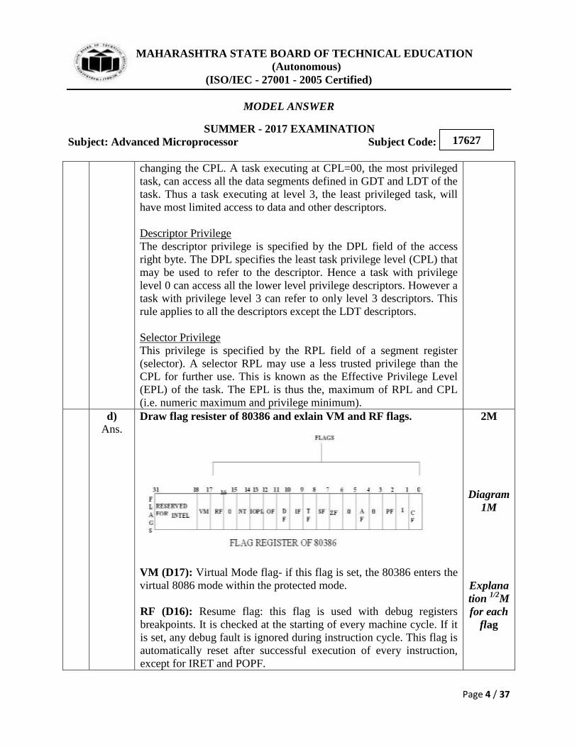
d)
Ans. Draw flag resister of 80386 and exlain VM and RF flags.
VM (D17): Virtual Mode flag- if this flag is set, the 80386 enters the
virtual 8086 mode within the protected mode.
RF (D16): Resume flag: this flag is used with debug registers
breakpoints. It is checked at the starting of every machine cycle. If it
is set, any debug fault is ignored during instruction cycle. This flag is
automatically reset after successful execution of every instruction,
except for IRET and POPF.
2M
Diagram
1M
Explana
tion 1/2
M
for each
flag
MAHARASHTRA STATE BOARD OF TECHNICAL EDUCATION
(Autonomous)
(ISO/IEC - 27001 - 2005 Certified)
MODEL ANSWER
SUMMER - 2017 EXAMINATION
Subject: Advanced Microprocessor Subject Code:
Page 5 / 37
17627
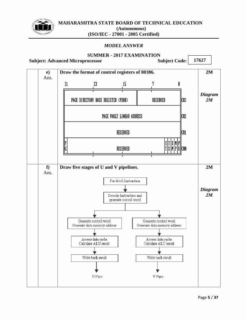
e)
Ans. Draw the format of control registers of 80386.
2M
Diagram
2M
f)
Ans. Draw five stages of U and V pipelines.
2M
Diagram
2M

MAHARASHTRA STATE BOARD OF TECHNICAL EDUCATION
(Autonomous)
(ISO/IEC - 27001 - 2005 Certified)
MODEL ANSWER
SUMMER - 2017 EXAMINATION
Subject: Advanced Microprocessor Subject Code:
Page 6 / 37
17627
g)
Ans. What is an interrupt?
Interrupt:
An interrupt is an external pulse/ signal or an internal instruction
that causes the microprocessor to temporarily work on a different
task, and then later return to its previous task. Interrupts can be
internal or external. The microprocessor responds to that interrupt
with an ISR (Interrupt Service Routine), which is a short program to
instruct the microprocessor on how to handle the interrupt. And after
executing the ISR, microprocessor returns back to main program
where it was stopped.
2M
Explana
tion 2M
h)
Ans. State the functions performed by IRET instruction.
IRET: Return from interrupt
After the completion of ISR (Interrupt Service Routine), it decodes
the instruction IRET.
While decoding this instruction, it retrieves the main program address
(PC from which next instruction of the interrupted program is to be
executed) & status of flag register of interrupted program (while
switching to ISR) from stack memory.
2M
Explana
tion 2M
i)
Ans. What is processor architecture?
Processor architecture:
The architecture of microprocessor chip is a description of the
physical layout of the various elements that form it. It directly affects
how information and electrical current flows throughout the chip.
The basic components of microprocessor architecture include:
ALU: The Arithmetic Logic Unit performs all arithmetic and logic
operations.
Accumulator: Holds the operands are results of operations
performed by the ALU.
PC (program counter): Holds the memory address of the next
instruction to be executed.
Status, data and address registers: The status register stores
information about the result of a previous ALU operation, the data
register stores data going to or coming from an I/O port or memory,
and the address register stores the address of the memory location to
be accessed.
Control unit: Holds the circuitry that controls the process of
executing, decoding and fetching program instructions.
2M
Explana
tion 2M
MAHARASHTRA STATE BOARD OF TECHNICAL EDUCATION
(Autonomous)
(ISO/IEC - 27001 - 2005 Certified)
MODEL ANSWER
SUMMER - 2017 EXAMINATION
Subject: Advanced Microprocessor Subject Code:
Page 7 / 37
17627
j)
Ans. What is meant by superscale machine?
Parallel execution of several instructions means superscalar
processor.
Eg. Pentium is a superscalar processor as it has 2 integer pipelines
U&V, these are responsible for execution of integer instructions.
These pipelines execute 2 integer instructions simultaneously.
2M
Explana
tion 2M
k)
Ans. What is predefined or dedicaed interrrupt?
INT 0(Divide by zero error)
The interrupt with type number 0 is dedicated to the divide by zero
error. This interrupt is an ‘error generated’ interrupt (also called an
‘exception’).
INT 1 (single stepping)
This type number is dedicated for single stepping or trace. Single
stepping is an important idea in debugging during logical debugging
of our programs.
INT 2 (Non Maskable Interrupt)
This interrupt corresponds to the vector (pointer) of the hardware
interrupt NMI. When an interrupt is received on the pin NMI (Non
Maskable Interrupt) of the processor, a type 2 interrupt occur- this
means that the ISR for NMI must be written in the address pointed by
the corresponding IVT content.
INT 3 (Breakpoint Interrupt)
This is the breakpoint interrupt, which is useful for de-bugging. We
will need to set breakpoints (stop after executing a group of
instruction) and check the content of registers and memory after
executing instructions up to the breakpoint.
INT 4 (Overflow Interrupt)
This interrupts corresponding to the overflow flag. If the overflow
flag is set, this interrupt occurs but not automatically. An instruction
INTO (interrupt on overflow) must be written after the program
segment which is likely to cause the overflow flag (OF) to be set.
2M
Explana
tion 2M
l)
Ans. State the function of register window in RISC processors.
The reduced hardware requirements of RISC processors leave
additional space available on the chip for the system designer. RISC
CPUs generally use this space to include a large number of registers
2M
MAHARASHTRA STATE BOARD OF TECHNICAL EDUCATION
(Autonomous)
(ISO/IEC - 27001 - 2005 Certified)
MODEL ANSWER
SUMMER - 2017 EXAMINATION
Subject: Advanced Microprocessor Subject Code:
Page 8 / 37
17627
(> 100 occasionally).
The CPU can access data in registers more quickly than data in
memory so having more registers makes more data available faster.
Having more registers also helps reduce the number of memory
references especially when calling and returning from subroutines.
Register windows provide their greatest benefit when the CPU calls a
subroutine. During the calling process, the register window is moved
down 1 window position. In the SPARC CPU, if window 1 is active
and the CPU calls a subroutine, the processor activates window 2 by
updating the window pointer and window mask registers. The CPU
can pass parameters to the subroutine via the registers that overlap
both windows instead of memory. This saves a lot of time when
accessing data. The CPU can use the same registers to return results
to the calling routine.
Functio
n of
register
window
in RISC
processo
rs 2M
m)
Ans. What is an exception interrupt?
Exceptions are the interrupts which when occur must be processed
by the processor. They don’t allow the processor to execute the
remaining part of the program unless they are processed.
Exceptions take the control of execution to some other part for their
processing which is executed by the processor.
Processor exceptions are: Divide Error (Type 0), Unused opcode
(type 6) and Escape opcode (type 7).
2M
Explana
tion 2M
n)
Ans. State two characterisitcs of cache memory.
Characterisitcs of cache memory:
1.The separate cache memories raise the system performance i.e. an
internal read request is performed more quickly than a bus cycle to
memory.
2.They reduce the use of processor’s external bus when the same
locations are accessed multiple times.
2M
Two
characte
ristics
2M
o)
Ans. What is load and store architecture?
Load and store architecture: the RISC architecture is primarily load
and store architecture, implying that all the memory accesses take
place using Load and Store type operations. Load is similar to read
operation and store is similar to the write operation.
2M
Explana
tion 2M
MAHARASHTRA STATE BOARD OF TECHNICAL EDUCATION
(Autonomous)
(ISO/IEC - 27001 - 2005 Certified)
MODEL ANSWER
SUMMER - 2017 EXAMINATION
Subject: Advanced Microprocessor Subject Code:
Page 9 / 37
17627
2.
a)
Ans.
Solve any two questions:
Compare pentium, pentium -2 and pentium-3 processors (any
four points).
Parameter Pentium Pentium-2 Pentium-3
Clock Speed 60 MHZ 233 MHZ 450 MHZ
Data Width 32 bits, 64 bit
bus
32 bits, 64 bit
bus
32 bits, 64 bit
bus
MIPS 100 ~300 ~510
Number of
Transistors
3,100,000
(0.8 micron)
7,500,000
(0.35 micron)
24,000,000
(0.13 micron)
Addressable
Memory
4GB 64GB 64GB
16
8M
Any 4
points
2M each
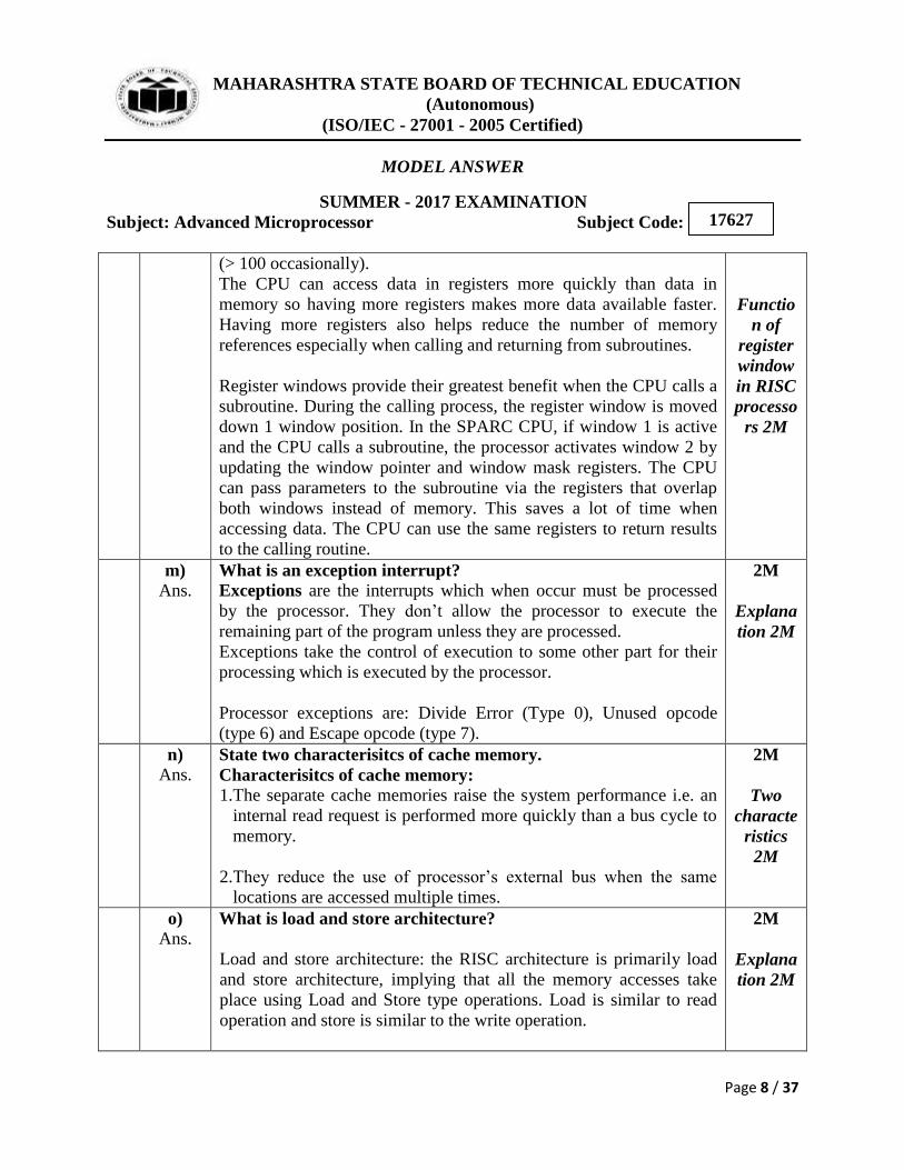
b)
Ans.
Draw page translation mechanism and explain paging mode of
80386.
The paging unit operates under the control of segmentation unit. The
paging unit if enabled converts linear addresses into physical address,
in protected mode.
•Paging Operation: Paging is one of the memory management
techniques used for virtual memory multitasking operating system.
•The segmentation scheme may divide the physical memory into a
variable size segments but the paging divides the memory into a fixed
8M
Diagram
4M
Explana
tion 4M

MAHARASHTRA STATE BOARD OF TECHNICAL EDUCATION
(Autonomous)
(ISO/IEC - 27001 - 2005 Certified)
MODEL ANSWER
SUMMER - 2017 EXAMINATION
Subject: Advanced Microprocessor Subject Code:
Page 10 / 37
17627
size pages.
•The segments are supposed to be the logical segments of the
program, but the pages do not have any logical relation with the
program.
•The pages are just fixed size portions of the program module or data.
•The advantage of paging scheme is that the complete segment of a
task need not be in the physical memory at any time.
•Only a few pages of the segments, which are required currently for
the execution need to be available in the physical memory. Thus the
memory requirement of the task is substantially reduced,
relinquishing the available memory for other tasks.
•Whenever the other pages of task are required for execution, they
may be fetched from the secondary storage.
•The previous page which are executed, need not be available in the
memory, and hence the space occupied by them may be relinquished
for other tasks.
•Thus paging mechanism provides an effective technique to manage
the physical memory for multitasking systems.
•Paging Unit: The paging unit of 80386 uses a two level table
mechanism to convert a linear address provided by segmentation unit
into physical addresses.
The paging unit converts the complete map of a task into pages, each
of size 4K. The task is further handled in terms of its page, rather than
segments.
The paging unit handles every task in terms of three components
namely page directory, page tables and page itself.
•Paging Descriptor Base Register: The control register CR2 is used
to store the 32-bit linear address at which the previous page fault was
detected.
The CR3 is used as page directory physical base address register, to
store the physical starting address of the page directory.
The lower 12 bit of the CR3 are always zero to ensure the page size
aligned directory. A move operation to CR3 automatically loads the
page table entry caches and a task switch operation, to load CR0
suitably.
•Page Directory: This is at the most 4Kbytes in size. Each directory
entry is of 4 bytes, thus a total of 1024 entries are allowed in a
directory. The upper 10 bits of the linear address are used as an index
to the corresponding page directory entry. The page directory entries

MAHARASHTRA STATE BOARD OF TECHNICAL EDUCATION
(Autonomous)
(ISO/IEC - 27001 - 2005 Certified)
MODEL ANSWER
SUMMER - 2017 EXAMINATION
Subject: Advanced Microprocessor Subject Code:
Page 11 / 37
17627
point to page tables.
•Page Tables: Each page table is of 4Kbytes in size and many
contain a maximum of 1024 entries. The page table entries contain
the starting address of the page and the statistical information about
the page.
•The upper 20 bit page frame address is combined with the lower 12
bit of the linear address. The address bits A12- A21 are used to select
the 1024 page table entries. The page table can be shared between the
tasks.
c)
Ans. Draw the internal architecture of 80386 processor and explain.
The internal architecture of 80386 can be divided into 3 sections
such as
1. Central processing unit (CPU)
2. Memory management unit (MMU)
3. Bus interface unit (BIU)
The Central processing unit consists of
Execution unit & Instruction unit Instruction unit has Instruction pre-fetcher and instruction pre-decode
unit
8M
Diagram
4M
Explana
tion 4M
MAHARASHTRA STATE BOARD OF TECHNICAL EDUCATION
(Autonomous)
(ISO/IEC - 27001 - 2005 Certified)
MODEL ANSWER
SUMMER - 2017 EXAMINATION
Subject: Advanced Microprocessor Subject Code:
Page 12 / 37
17627
The Instruction pre-fetcher fetches the 16 instruction bytes ahead of
time and stores them into the 16 byte instruction pre-fetch queue(16
byte code).This speeds up the program execution process.
The instruction pre-decode unit has the instruction decoder and 3
decoded instruction queue.
The instruction decoder decodes 3 instructions ahead of time and
stores them in the 3 decoded instruction queue.
Execution unit has ALU and control unit.
The control unit stores the control signals in the control ROM, which
are generated at the time of decoding .The decode and sequencing
unit decodes the control signals and sends the control signals
sequentially to the ALU.
ALU (arithmetic and logic unit): ALU performs all the arithmetic and
logical operations. It has a register file containing registers such as
general purpose registers, control and flag registers, debug and test
registers, special purpose registers etc. The barrel shifter is of 64 bits
which can shift/rotate 64 bits at a time and hence can perform
multiplication and divide operations within a microsecond.
The memory management unit has segmentation unit and paging
unit. The segmentation unit allows the use of two address components
such as segment base address and offset address to calculate the
physical address. It allows the size of the segment upto 4GB
maximum. It provides the 4 level protection level mechanism for
protecting and isolating the system’s code and data from application
programs and unauthorized access. This unit converts logical address
spaces to the linear addresses. The Limit and Attribute PLA checks
the segment limits and attributes at segment level to avoid invalid
access to the code
The paging unit converts the linear addresses to the physical
addresses. The control and attribute PLA checks the privileges at
page level. Each of the pages maintain the paging information of the
task. The paging unit organizes the physical memory in the terms of
pages of 4KB each. This unit works under the control of
segmentation unit i.e., each segment is further divided into pages. The
virtual memory is also organized in the terms of segments and pages
by the MMU.
The BIU has a bus control unit which has a request prioritizer which

MAHARASHTRA STATE BOARD OF TECHNICAL EDUCATION
(Autonomous)
(ISO/IEC - 27001 - 2005 Certified)
MODEL ANSWER
SUMMER - 2017 EXAMINATION
Subject: Advanced Microprocessor Subject Code:
Page 13 / 37
17627
resolves the priorities of the various bus request operations. It also
controls the access of the bus. The address drivers drives the bus
(byte) enable signals BE0#-BE3# and the address signals A0-A31.
The pipeline and bus size control unit handle the related control
signals and supports the dynamic bus sizing feature. The data buffers
(mux/ transceivers) interface the internal data bus with the system
data bus.
3.
a)
Ans.
Solve any four questions:
Explain (PVAM) Protected Virtual Adderssing Mode of 80386.
Address calculation in protected mode: Address generation in
PVAM: In PVAM there are two components. A 16-bit selector which
determines the linear base address of a segment and the base address
is added to a 32-bit effective address to form a 32 bit linear address.
The linear address is used as the 32-bit physical address or if paging
is enabled the paging mechanism maps the 32-bit linear address into a
32 physical address. The selector is used to specify an index into an
OS defined table that contains the 32-bit base address of given
segment. The physical address is formed by adding the base address
obtained from the table to the offset. Paging provides additional
memory management that operates only in PVAM. It provides a
mean of managing large segments of memory. The paging
mechanism translates the protected linear address from segmentation
unit into a physical address.
OR
16
4M
Descript
ion 2M
Diagram
2M
MAHARASHTRA STATE BOARD OF TECHNICAL EDUCATION
(Autonomous)
(ISO/IEC - 27001 - 2005 Certified)
MODEL ANSWER
SUMMER - 2017 EXAMINATION
Subject: Advanced Microprocessor Subject Code:
Page 14 / 37
17627
b)
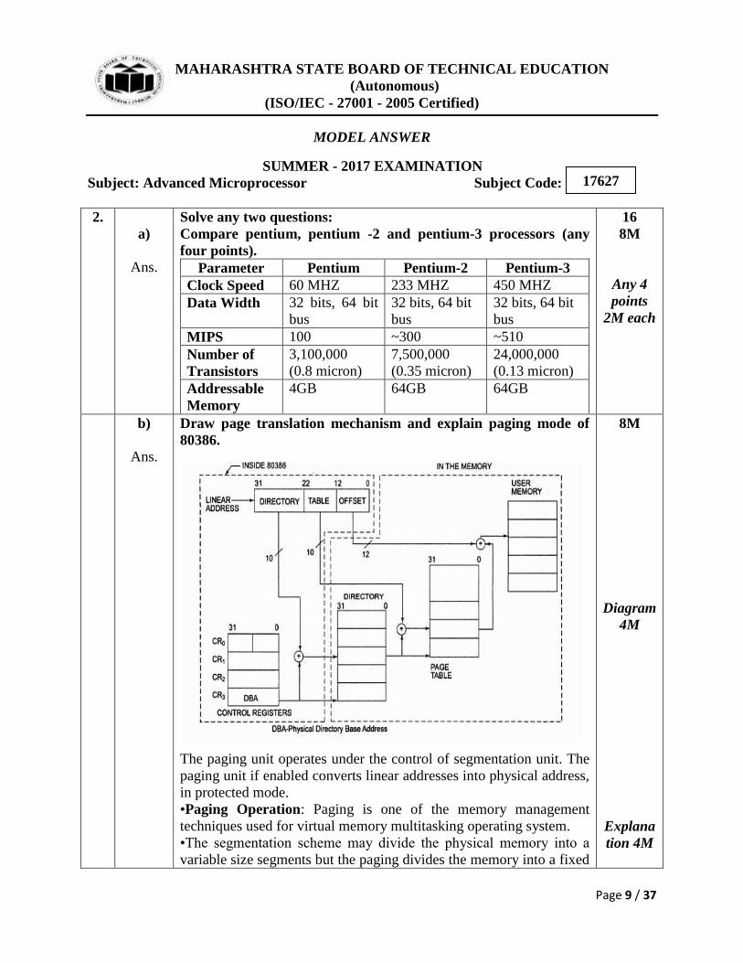
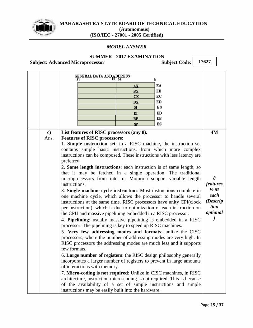
Ans. Enlist and explain general purpose registers of 80386 processor.
General Purpose Registers:
1. EAX
2. EBX
3. ECX
4. EDX
5. ESI
6. EDI
7. EBP
8. ESP
Description
• The 80386 has eight 32 - bit general purpose registers which may be
used as either 8 bit or 16 bit registers.
• A 32 - bit register known as an extended register, is represented by
the register name with prefix E.
• Example : A 32 bit register corresponding to AX is EAX, similarly
BX is EBX etc.
• The 16 bit registers BP, SP, SI and DI in 8086 are now available
with their extended size of 32 bit and are names as EBP, ESP, ESI
and EDI.
• AX represents the lower 16 bit of the 32 bit register EAX.
• BP, SP, SI, DI represents the lower 16 bit of their 32 bit
counterparts, and can be used as independent 16 bit registers.
4M
List 1M
Descript
ion 3M
MAHARASHTRA STATE BOARD OF TECHNICAL EDUCATION
(Autonomous)
(ISO/IEC - 27001 - 2005 Certified)
MODEL ANSWER
SUMMER - 2017 EXAMINATION
Subject: Advanced Microprocessor Subject Code:
Page 15 / 37
17627
c)
Ans. List features of RISC processors (any 8).
Features of RISC processors:
1. Simple instruction set: in a RISC machine, the instruction set
contains simple basic instructions, from which more complex
instructions can be composed. These instructions with less latency are
preferred.
2. Same length instructions: each instruction is of same length, so
that it may be fetched in a single operation. The traditional
microprocessors from intel or Motorola support variable length
instructions.
3. Single machine cycle instruction: Most instructions complete in
one machine cycle, which allows the processor to handle several
instructions at the same time. RISC processors have unity CPI(clock
per instruction), which is due to optimization of each instruction on
the CPU and massive pipelining embedded in a RISC processor.
4. Pipelining: usually massive pipelining is embedded in a RISC
processor. The pipelining is key to speed up RISC machines.
5. Very few addressing modes and formats: unlike the CISC
processors, where the number of addressing modes are very high. In
RISC processors the addressing modes are much less and it supports
few formats.
6. Large number of registers: the RISC design philosophy generally
incorporates a larger number of registers to prevent in large amounts
of interactions with memory.
7. Micro-coding is not required: Unlike in CISC machines, in RISC
architecture, instruction micro-coding is not required. This is because
of the availability of a set of simple instructions and simple
instructions may be easily built into the hardware.
4M
8
features
½ M
each
(Descrip
tion
optional
)

MAHARASHTRA STATE BOARD OF TECHNICAL EDUCATION
(Autonomous)
(ISO/IEC - 27001 - 2005 Certified)
MODEL ANSWER
SUMMER - 2017 EXAMINATION
Subject: Advanced Microprocessor Subject Code:
Page 16 / 37
17627
8. Load and Store architecture: the RISC architecture is primarily a
Load and Store architecture, implying that all the memory accesses
takes place using Load and Store type operations.
d)
Ans. State any four differences between .COM and .EXE programs.
Sr.
No.
.COM .EXE
1 .COM file does not
contain any header
.EXE file contains header
2 .COM file cannot contain
relocation items.
.EXE file may contain
relocation items.
3 Maximum size is 64k
minus 256 bytes.
For PSP and 2 bytes for
stack
No limit on size; Can be of
any size
4 Entry point is PSP:0100
Entry point is defined by END
directive.
5 Stack size is 64K minus
256 bytes for PSP and
size of executable data
and code.
Stack size is defined in a
program with STACK
directive
6 Size of file is exact size
of program.
Size of file is size of program
plus header (Multiple of 256
bytes)
4M
Any 4
differen
ces
between
.com
and .exe
program
1M
each
e)
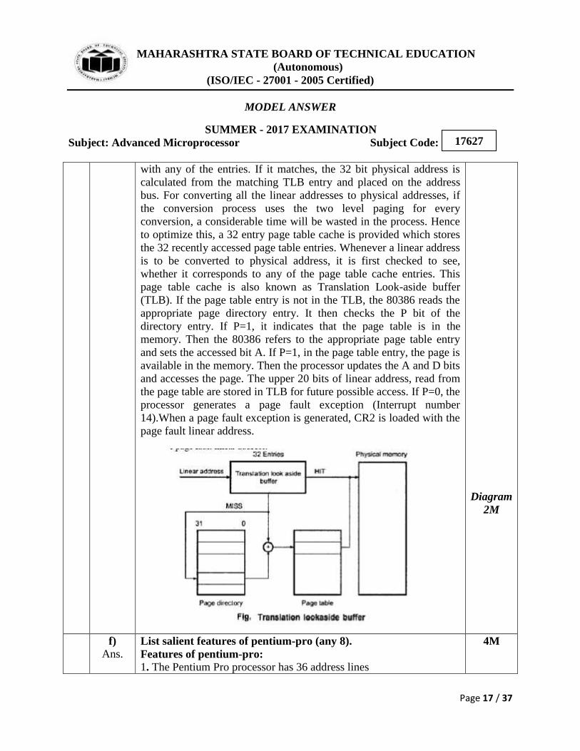
Ans. Draw paging operation diagram using TLB and explain.
Paging mechanism with TLB: As the conversion of 32 bits linear address to physical address is too
longer, the Paging unit of 80386 uses TLB.
The paging unit receives a 32 bit linear address from the
segmentation unit. The structure of linear address is shown below.
The upper 20 linear address bits (A12 – A31) are compared with all
the entries in the translation look aside buffer to check if it matches
4M
Descript
ion 2M
MAHARASHTRA STATE BOARD OF TECHNICAL EDUCATION
(Autonomous)
(ISO/IEC - 27001 - 2005 Certified)
MODEL ANSWER
SUMMER - 2017 EXAMINATION
Subject: Advanced Microprocessor Subject Code:
Page 17 / 37
17627
with any of the entries. If it matches, the 32 bit physical address is
calculated from the matching TLB entry and placed on the address
bus. For converting all the linear addresses to physical addresses, if
the conversion process uses the two level paging for every
conversion, a considerable time will be wasted in the process. Hence
to optimize this, a 32 entry page table cache is provided which stores
the 32 recently accessed page table entries. Whenever a linear address
is to be converted to physical address, it is first checked to see,
whether it corresponds to any of the page table cache entries. This
page table cache is also known as Translation Look-aside buffer
(TLB). If the page table entry is not in the TLB, the 80386 reads the
appropriate page directory entry. It then checks the P bit of the
directory entry. If P=1, it indicates that the page table is in the
memory. Then the 80386 refers to the appropriate page table entry
and sets the accessed bit A. If P=1, in the page table entry, the page is
available in the memory. Then the processor updates the A and D bits
and accesses the page. The upper 20 bits of linear address, read from
the page table are stored in TLB for future possible access. If P=0, the
processor generates a page fault exception (Interrupt number
14).When a page fault exception is generated, CR2 is loaded with the
page fault linear address.
Diagram
2M
f)
Ans. List salient features of pentium-pro (any 8).
Features of pentium-pro:
1. The Pentium Pro processor has 36 address lines
4M
MAHARASHTRA STATE BOARD OF TECHNICAL EDUCATION
(Autonomous)
(ISO/IEC - 27001 - 2005 Certified)
MODEL ANSWER
SUMMER - 2017 EXAMINATION
Subject: Advanced Microprocessor Subject Code:
Page 18 / 37
17627
2. The Pentium Pro processor has an additional 256/512 KB L2 cache
memory on chip.
3. On chip L2 cache speeds processing and reduces the number of
components in a system.
4. The L2 cache is connected to BIU, BIU generates memory
addresses and control signals and passes or fetches data or
instructions either to L1 data cache or L1 instruction cache.
5. The Instruction Fetch and Decode Unit (IFDU), contains three
separate: instruction decoders that decode three instructions
simultaneously
6. It also includes Branch Prediction Logic.
7. It predicts if the branch will be taken or not for a conditional jump
instruction.
8. The instruction are then put into the instruction pool.
9. The instruction pool is a memory accessible with its content.
10.The execute unit consists of three units namely two integer
execution unit and one floating point unit , two integer and one
floating instruction can be executed simultaneously
11. Pentium Pro also has one jump execution unit (address generation
unit).
12. The scheduling is performed by reservation station (RS) which
can schedule up to five events for execution and process four
simultaneously
Any 8
points
½ M
each
4.
a)
Ans.
Solve any four questions:
Compare RISC and CISC architectures:
RISC CISC
Acronym It stands for ‘Reduced
Instruction Set Computer’.
It stands for
‘Complex
Instruction Set
Computer
Definition The RISC processors have
a smaller set of instructions
with few addressing nodes.
The CISC
processors have a
larger set of
instructions with
many addressing
nodes.
Emphasis Emphasis on software Emphasis on
hardware
Memory unit It has no memory unit and It has a memory unit
16
4M
Any 4
differen
ces
between
RISC
and
CISC
1M
each

MAHARASHTRA STATE BOARD OF TECHNICAL EDUCATION
(Autonomous)
(ISO/IEC - 27001 - 2005 Certified)
MODEL ANSWER
SUMMER - 2017 EXAMINATION
Subject: Advanced Microprocessor Subject Code:
Page 19 / 37
17627
uses a separate hardware to
implement instructions.
to implement
complex
instructions.
Program It has a hard-wired unit of
programming
It has a micro-
programming unit.
Time Execution time is very
less.
Execution time is
very high
Design It is a complex complier
design.
It is an easy
complier design.
Applications Used in high end
applications such as video
processing,
telecommunications and
image processing.
Used in low end
applications such as
security systems,
home automations,
etc.
b)
Ans. Explain interrupt processing sequence of x86 processors.
Interrupt processing sequence is as given below: When INT n
instruction is executed:
1. The processor pushes flag register on stack then the contents of CS
and IP register on stack
2. It clears two flags TF (trap flag) and IE (Interrupt enable flag).
3. Number of interrupt is used to find correct address of ISR in the
IVT.
4. Interrupt number (is called as interrupt type) is used to find out the
correct address of ISR in the IVT.
5. The interrupt number is multiplied by 4 to get the address with the
IVT that contains the addresses of ISR.
ISR ADDRESS = Interrupt type x 4
6. All addresses are 4 bytes long. The Interrupt vector address is then
filled in CS and IP register.
7. Finally CPU control is transferred to new address.
8. It decrements stack pointer by 2 & push flag register on stack.
9. It clears the interrupt request by clearing interrupt flag.
10. It also reset trap flag in flag register.
11. Decrement stack pointer by 2 & store code segment in it.
12. Decrement stack pointer by 2 & pushes IP in it.
13. If fetches the ISR & jumps on it.
After the completion of ISR, it decodes the instruction IRET &
retrieves the main program address & status of flag register.
4M
Descript
ion of
sequenc
e 2M

MAHARASHTRA STATE BOARD OF TECHNICAL EDUCATION
(Autonomous)
(ISO/IEC - 27001 - 2005 Certified)
MODEL ANSWER
SUMMER - 2017 EXAMINATION
Subject: Advanced Microprocessor Subject Code:
Page 20 / 37
17627
Diagram
2M
c)
Ans. Draw code/data descriptor and explain.
•DESCRIPTORS: The 80386 descriptors have a 20-bit segment
limit and 32-bit segment address. The descriptor of 80386 are 8-byte
quantities access right or attribute bits along with the base and limit
of the segments.
•Descriptor Attribute Bits: The A (accessed) attributed bit indicates
whether the segment has been accessed by the CPU or not.
•The TYPE field decides the descriptor type and hence the segment
type.
•The S bit decides whether it is a system descriptor (S=0) or
code/data segment descriptor(S=1).
•The DPL field specifies the descriptor privilege level.
•The D bit specifies the code segment operation size. If D=1, the
segment is a 32-bit operand segment, else, it is a 16-bit operand
segment.
•The P bit (present) signifies whether the segment is present in the
physical memory or not. If P=1, the segment is present in the
physical memory.
•The G (granularity) bit indicates whether the segment is page
addressable. The zero bit must remain zero for compatibility with
future process.
•The AVL (available) field specifies whether the descriptor is for user
4M
Descript
ion 2M
MAHARASHTRA STATE BOARD OF TECHNICAL EDUCATION
(Autonomous)
(ISO/IEC - 27001 - 2005 Certified)
MODEL ANSWER
SUMMER - 2017 EXAMINATION
Subject: Advanced Microprocessor Subject Code:
Page 21 / 37
17627
or for operating system.
•The 80386 has five types of descriptors listed as follows:
1. Code or Data Segment Descriptors.
Diagram
2M
d)
Ans. List salient featues of sun ultra SPARC processor (any 8).
It contains an integer unit, a FPU and a optional coprocessor.
The 64 bits Ultra SPARC architecture has following features :
1. It has 14 stages non-stalling pipeline.
2. It has 6 execution units including two for integer, two for floating
point, one for load/store and one for address generation units.
3. It has a large number of buffers but only one load/store unit, it
dispatches them one instruction at a time from the instruction
stream.
4. It contains 32KB L1 instruction cache, 64KB L1 data cache, 2KB
prefetch cache and 2 KB write cache. It also has 1MB on chip L2
cache.
5. Like Pentium MMX it also contains the instructions to support
multimedia. These instructions are helpful for the implementation
of image processing codes.
6. One of the major limitations of SPARC system is its low speed
compared to most of the modern processors.
7. SPARC stores multi-byte numbers using BIG Indian format, i.e.
the MSB will be stored at the lowest memory address.
8. It supports a pipelined floating point processor. The FPU has 5
separate functional units for performing the floating point
operations. The floating point instructions can be issued per cycle
4M
Any
eight
features
of sun
ultra
SPARC
processo
r ½ M
each
MAHARASHTRA STATE BOARD OF TECHNICAL EDUCATION
(Autonomous)
(ISO/IEC - 27001 - 2005 Certified)
MODEL ANSWER
SUMMER - 2017 EXAMINATION
Subject: Advanced Microprocessor Subject Code:
Page 22 / 37
17627
and executed by the FPU unit.
The source and data results are stored in 32 register files. Majority of
the floating point instructions have a throughput of one cycle and a
latency of three cycles. Although the single precision (32 bit) or
double precision (64 bit) floating point computations can be
performed by hardware, quad precision i.e. 128 bits operation can be
performed only in the software.
e)
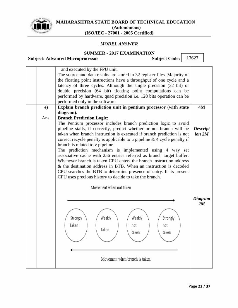
Ans.
Explain branch prediction unit in pentium processor (with state
diagram).
Branch Prediction Logic:
The Pentium processor includes branch prediction logic to avoid
pipeline stalls, if correctly, predict whether or not branch will be
taken when branch instruction is executed if branch prediction is not
correct recycle penalty is applicable to u pipeline & 4 cycle penalty if
branch is related to v pipeline.
The prediction mechanism is implemented using 4 way set
associative cache with 256 entries referred as branch target buffer.
Whenever branch is taken CPU enters the branch instruction address
& the destination address in BTB. When an instruction is decoded
CPU searches the BTB to determine presence of entry. If its present
CPU uses precious history to decide to take the branch.
4M
Descript
ion 2M
Diagram
2M

MAHARASHTRA STATE BOARD OF TECHNICAL EDUCATION
(Autonomous)
(ISO/IEC - 27001 - 2005 Certified)
MODEL ANSWER
SUMMER - 2017 EXAMINATION
Subject: Advanced Microprocessor Subject Code:
Page 23 / 37
17627
f)
Ans. Draw superscalar architecture of pentium processor.
4M
Labeled
architect
ure of
Pentium
processo
r :4M
5.
a)
Ans.
Solve any four questions:
Draw system descriptor cache register of 80386 microprocessor.
Explain.
Diagram of system descriptor cache register of 80386microprocessor
is as follows:
These registers are not available for the users.
These registers are associated with the segments and the segment
16
4M
system
descript
or cache
register
of
80386mi
croproce
ssor
diagram
2M
MAHARASHTRA STATE BOARD OF TECHNICAL EDUCATION
(Autonomous)
(ISO/IEC - 27001 - 2005 Certified)
MODEL ANSWER
SUMMER - 2017 EXAMINATION
Subject: Advanced Microprocessor Subject Code:
Page 24 / 37
17627
registers in 80386 i.e.
CS,DS,ES,SS,FS,GS
Every segment descriptor cache register is 72 bits long.
Every segment descriptor cache register holds
a. 32 bits segment base address
b. 32 bits segment limit
c. Other required segment attributes.
When a selector is loaded, its associated segment descriptor cache
register is automatically get loaded with the values from
descriptor table. Either from LDT or GDT.
In the real mode, only the base address is updated directly by
shifting the selector values 4 bits to the left.
In the protected mode, the base address, limit and all attributes are
loaded.
Descript
ion 2M
b)
Ans.
List floating point exceptions of pentium processor and explain
any one.
The Pentium provides 6 floating point exceptions:
1. Invalid operation
2. Divide by zero
3. De-normalized operand
4. Numeric overflow
5. Numeric underflow
6. Inexact result
1. Invalid operation
The floating point invalid exception occurs in response to two
general types of operations :
Stack overflow or underflow
Invalid arithmetic operand.
When the SF is set to 1, a stack operation has resulted in stack
overflow or underflow. When the flag is cleared to 0, an arithmetic
instruction has encountered an invalid operation.
The FPU explicitly sets the SF flag when it detects a stack overflow
or underflow condition, but it does not explicitly clear the flag when
it detects an invalid arithmetic operand condition.
As a result the state of the SF flag can be 1 following an invalid
arithmetic operation exception, if it was not cleared from the last time
a stack overflow or underflow condition occurred.
2. Divide by zero:
4M
List of
floating
point
exceptio
ns of
Pentium
processo
r 1M
Descript
ion of
any one
3M
MAHARASHTRA STATE BOARD OF TECHNICAL EDUCATION
(Autonomous)
(ISO/IEC - 27001 - 2005 Certified)
MODEL ANSWER
SUMMER - 2017 EXAMINATION
Subject: Advanced Microprocessor Subject Code:
Page 25 / 37
17627
The FPU reports a floating point zero divide exception, whenever an
instruction attempts to divide the operand by 0.
The flag ZE for this exception is bit 2 of the FPU status word, and the
mask bit ZM is bit 2 of the control word.
The FDIV, FDIVP, FDIVR, FDIVRP, FIDIV, FIDIVR instructions
and the other instructions that perform division internally can report
the divide by zero exception.
3. De-normalized operand
The FPU signals the de-normal operand exception under the
following conditions:
1. If an arithmetic instruction attempts to operate on a denormal
operand.
2. If an attempt is made to load the denormal single or double real
value into an FPU register.
The flag DE for this exception is bit 1 of the FPU status word, and
the mask bit (DM) is the 1 of the FPU control word.
4. Numeric overflow
This exception occurs when the rounded result of an arithmetic
instruction exceeds the largest allowable finite value that will fit into
the real format of the destination operand.
5. Numeric underflow
This exception occurs when the rounded result of an arithmetic
instruction is less than the smallest possible normalized ,finite value
that will fit into the real format of the destination operand.
6. Inexact result
This exception occurs if the result of an operation is not exactly in
represent able in the destination format.
c)
Ans. List BIOS interrupts and explain any two.
Various BIOS interrupts are:
1. INT 10H
2. INT 16H
3. INT 17H
4. INT 25H
1. INT 17h: Printer Services
4M
List of
any 4
BIOS
interrupt
s 1M
MAHARASHTRA STATE BOARD OF TECHNICAL EDUCATION
(Autonomous)
(ISO/IEC - 27001 - 2005 Certified)
MODEL ANSWER
SUMMER - 2017 EXAMINATION
Subject: Advanced Microprocessor Subject Code:
Page 26 / 37
17627
BIOS Operation: Print data and test the printer status
Parameters: ax, dx
Int 17h controls the parallel printer interfaces on the IBM PC.
Int 17h provides three subfunctions, specified by the value in
the ah register. These subfunctions are:
0-Print the character in the AL register.
1-Initialize the printer.
2-Return the printer status.
Each of these functions is described in the following sections.
Like the serial port services, the printer port services allow you to
specify which of the three printers installed in the system you wish to
use (LPT1:, LPT2:, or LPT3:). The value in the dx register (0..2)
specifies which printer port is to be used.
One final note- under DOS it's possible to redirect all printer output
to a serial port. This is quite useful if you're using a serial printer. The
BIOS printer services only talk to parallel printer adapters. If you
need to send data to a serial printer using BIOS, you'll have to use int
14h to transmit the data through a serial port.
1. AH=0: Print a Character:
If ah is zero when you call int 17h, then the BIOS will print the
character in the al register. Exactly how the character code in
the al register is treated is entirely up to the printer device you're
using. Most printers, however, respect the printable ASCII character
set and a few control characters as well. Many printers will also print
all the symbols in the IBM/ASCII character set (including European,
line drawing, and other special symbols). Most printers treat control
characters (especially ESC sequences) in completely different
manners. Therefore, if you intend to print something other than
standard ASCII characters, be forewarned that your software may not
work on printers other than the brand you're developing your software
on.
Upon return from the int 17h subfunction zero routine, the ah register
contains the current status. The values actually returned are described
in the section on subfunction number two.
2. AH=1: Initialize Printer
Executing this call sends an electrical impulse to the printer telling it
Explana
tion of
any 2
1½ M
each
MAHARASHTRA STATE BOARD OF TECHNICAL EDUCATION
(Autonomous)
(ISO/IEC - 27001 - 2005 Certified)
MODEL ANSWER
SUMMER - 2017 EXAMINATION
Subject: Advanced Microprocessor Subject Code:
Page 27 / 37
17627
to initialize itself. On return, the ah register contains the printer status
as per function number two.
3. AH=2: Return Printer Status This function call checks the printer status and returns it in
the ah register. The values returned are:
AH: Bit Meaning
7 1=Printer busy, 0=printer not busy
6 1=Acknowledge from printer
5 1=Out of paper signal
4 1=Printer selected
3 1=I/O error
2 Not used
1 Not used
0 Time out error
4. Acknowledge from printer is, essentially, a redundant signal (since
printer busy/not busy gives you the same information). As long as the
printer is busy, it will not accept additional data. Therefore, calling
the print character function (ah=0) will result in a delay.
The out of paper signal is asserted whenever the printer detects that it
is out of paper. This signal is not implemented on many printer
adapters. On such adapters it is always programmed to a logic zero
(even if the printer is out of paper). Therefore, seeing a zero in this bit
position doesn't always guarantee that there is paper in the machine.
Seeing a one here, however, definitely means that your printer is out
of paper.
The printer selected bit contains a one as long as the printer is on-line.
If the user takes the printer off-line, then this bit will be cleared.
The I/O error bit contains a one if some general I/O error has
occurred.
The time out error bit contains a one if the BIOS routine waited for an
extended period of time for the printer to become "not busy" yet the
printer remained busy.

MAHARASHTRA STATE BOARD OF TECHNICAL EDUCATION
(Autonomous)
(ISO/IEC - 27001 - 2005 Certified)
MODEL ANSWER
SUMMER - 2017 EXAMINATION
Subject: Advanced Microprocessor Subject Code:
Page 28 / 37
17627
Note that certain peripheral devices (other than printers) also
interface to the parallel port, often in addition to a parallel printer.
Some of these devices use the error/status signal lines to return data
to the PC. The software controlling such devices often takes over
the int 17h routine (via a technique we'll talk about later on) and
always returns a "no error" status or "time out error" status if an error
occurs on the printing device. Therefore, you should take care not to
depend too heavily on these signals changing when you make the int
17h BIOS calls.
2. INT 16h - Keyboard Services Instruction: int 16h
BIOS Operation: Read a key, test for a key, or get keyboard status
Parameters: al
The IBM PC BIOS provides several function calls dealing with the
keyboard. As with many of the PC BIOS routines, the number of
functions has increased over the years. This section describes the
three calls that were available on the original IBM PC.
AH=0: Read a Key From the Keyboard
If int 16h is called with ah equal to zero, the BIOS will not return
control to the caller until a key is available in the system type ahead
buffer. On return, al contains the ASCII code for the key read from
the buffer and ah contains the keyboard scan code. Keyboard scan
codes are described in the appendices.
Certain keys on the PC's keyboard do not have any corresponding
ASCII codes. The function keys, Home, PgUp, End, PgDn, the arrow
keys, and the Alt keys are all good examples. When such a key is
pressed, int 16h returns a zero in al and the keyboard scan code in ah.
Therefore, whenever an ASCII code of zero is returned, you must
check the ah register to determine which key was pressed.
Note that reading a key from the keyboard using the BIOS int
16h call does not echo the key pressed to the display. You have to
call putc or use int 10h to print the character once you've read it if
you want it echoed to the screen.
MAHARASHTRA STATE BOARD OF TECHNICAL EDUCATION
(Autonomous)
(ISO/IEC - 27001 - 2005 Certified)
MODEL ANSWER
SUMMER - 2017 EXAMINATION
Subject: Advanced Microprocessor Subject Code:
Page 29 / 37
17627
Example: Read a sequence of keystrokes from the keyboard until
Enter is pressed.
ReadLoop: mov ah, 0; Read Key opcode
int 16h
cmp al, 0; Special function?
jzReadLoop; If so, don't echo this keystroke
putc
cmp al, 0dh; Carriage return (ENTER)?
jneReadLoop
AH=1: See if a Key is Available at the Keyboard
This particular int 16h subfunction allows you to check to see if a key
is available in the system type ahead buffer. Even if a key is not
available, control is returned (right away!) to the caller. With this call
you can occasionally poll the keyboard to see if a key is available and
continue processing if a key hasn't been pressed (as opposed to
freezing up the computer until a key is pressed).
There are no input parameters to this function. On return, the zero
flag will be clear if a key is available, set if there aren't any keys in
the type ahead buffer. If a key is available, then ax will contain the
scan and ASCII codes for that key. However, this function will not
remove that keystroke from the type ahead buffer. Subfunction #0
must be used to remove characters. The following example
demonstrates how to build a random number generator using the test
keyboard function.
d)
Ans. Explain design issues of RISC processor.
Design issues of RISC processor are:
1.Register Window : The reduced hardware requirements of RISC processors leave
additional space available on the chip for the system designer. RISC
CPUs generally use this space to include a large number of registers (
> 100 occasionally).
The CPU can access data in registers more quickly than data in
memory so having more registers makes more data available faster.
Having more registers also helps reduce the number of memory
4M
design
issues of
Risc
processo
r :list
and
descripti
on 4M

MAHARASHTRA STATE BOARD OF TECHNICAL EDUCATION
(Autonomous)
(ISO/IEC - 27001 - 2005 Certified)
MODEL ANSWER
SUMMER - 2017 EXAMINATION
Subject: Advanced Microprocessor Subject Code:
Page 30 / 37
17627
references especially when calling and returning from subroutines.
The RISC processor may not be able to access all the registers it has
at any given time provided that it has many of it.
Most RISC CPUs have some global registers which are always
accessible. The remaining registers are windowed so that only a
subset of the registers are accessible at any specific time.
To understand how register windows work, we consider the
windowing scheme used by the Sun SPARC processor.
The processor can access any of the 32 different registers at a given
time. (The instruction formats for SPARC always use 5 bits to select
a source/destination register which can take any 32 different values.
Of these 32 registers, 8 are global registers that are always accessible.
The remaining 24 registers are contained in the register window.
The register window overlap. The overlap consists of 8 registers in
SPARC CPU. Notice that the organization of the windows are
supposed to be circular and not linear; meaning that the last window
overlaps with the first window.
Example: the last 8 registers of window 1 are also the first 8 registers
of window 2. Similarly, the last 8 registers of window 2 are also the
first 8 registers of window 3. The middle 8 registers of window 2 are
local; they are not shared with any other window.
The RISC CPU must keep track of which window is active and
which windows contain valid data. A window pointer register
contains the value of the window that is currently active. A
window mask register contains 1 bit per window and denotes
which windows contains valid data.
Register windows provide their greatest benefit when the CPU
calls a subroutine. During the calling process, the register window
is moved down 1 window position. In the SPARC CPU, if window
1 is active and the CPU calls a subroutine, the processor activates
window 2 by updating the window pointer and window mask
registers. The CPU can pass parameters to the subroutine via the
registers that overlap both windows instead of memory. This saves
a lot of time when accessing data. The CPU can use the same
registers to return results to the calling routine.
Drawbacks of register windowing is that on interactions with the
system, the registers need to be flushed to the stack, necessitating
the long sequence of writes to memory of data that is often mostly
MAHARASHTRA STATE BOARD OF TECHNICAL EDUCATION
(Autonomous)
(ISO/IEC - 27001 - 2005 Certified)
MODEL ANSWER
SUMMER - 2017 EXAMINATION
Subject: Advanced Microprocessor Subject Code:
Page 31 / 37
17627
garbage.
It opposes the multitasking workloads and by considering
compilers with poor optimization.
2. Pipelining in RISC :
A RISC processor pipeline operates in much the same way, although
the stages in the pipeline are different. While different processors
have different numbers of steps, they are basically variations of these
five, used in the MIPS R3000 processor:
1. Fetch instructions from memory
2. Read registers and decode the instruction
3. Execute the instruction or calculate an address
4. Access an operand in data memory
5. Write the result into a register
The length of the pipeline is dependent on the length of the longest
step. Because RISC instructions are simpler than those used in pre-
RISC processors (now called CISC, or Complex Instruction Set
Computer), they are more conducive to pipelining. While CISC
instructions varied in length, RISC instructions are all the same length
and can be fetched in a single operation. Ideally, each of the stages in
a RISC processor pipeline should take 1 clock cycle so that the
processor finishes an execution of every instruction in same time.
Pipeline Problems
In practice, however, RISC processors operate at more than one cycle
per instruction. The processor might occasionally stall a result of data
dependencies and branch instructions.
A data dependency occurs when an instruction depends on the results
of a previous instruction. A particular instruction might need data in a
register which has not yet been stored since that is the job of a
preceeding instruction which has not yet reached that step in the
pipeline.
Branch instructions are those that tell the processor to make a
decision about what the next instruction to be executed should be
based on the results of another instruction. Branch instructions can be
troublesome in a pipeline if a branch is conditional on the results of

MAHARASHTRA STATE BOARD OF TECHNICAL EDUCATION
(Autonomous)
(ISO/IEC - 27001 - 2005 Certified)
MODEL ANSWER
SUMMER - 2017 EXAMINATION
Subject: Advanced Microprocessor Subject Code:
Page 32 / 37
17627
an instruction which has not yet finished its path through the pipeline.
3. Single cycle instruction execution in RISC:
RISC designers are concerned primarily with creating the fastest chip
possible, and so they use a number of techniques, including
pipelining.
Pipelining is a design technique where the computer's hardware
processes more than one instruction at a time, and doesn't wait for
one instruction to complete before starting the next.
The four stages in our typical CISC machine are fetch, decode,
execute, and write. These same stages exist in a RISC machine, but
the stages are executed in parallel. As soon as one stage completes, it
passes on the result to the next stage and then begins working on
another instruction.
The performance of a pipelined system depends on the time it takes
only for any one stage to be completed-not on the total time for all
stages as with non-pipelined designs.
In an typical pipelined RISC design, each instruction takes 1 clock
cycle for each stage, so the processor can accept 1 new instruction per
clock. Pipelining doesn't improve the latency of instructions (each
instruction still requires the same amount of time to complete), but it
does improve the overall throughput.
As with CISC computers, the ideal is not always achieved.
Sometimes pipelined instructions take more than one clock to
complete a stage. When that happens, the processor has to stall and
not accept new instructions until the slow instruction has moved on to
the next stage.
Since the processor is sitting idle when stalled, both the designers and
programmers of RISC systems make a conscious effort to avoid
stalls. To do this, designers employ several techniques.
4. Dependencies
One problem that RISC programmers face is that the processor can be
slowed down by a poor choice of instructions. Since each instruction
takes some amount of time to store its result, and several instructions
MAHARASHTRA STATE BOARD OF TECHNICAL EDUCATION
(Autonomous)
(ISO/IEC - 27001 - 2005 Certified)
MODEL ANSWER
SUMMER - 2017 EXAMINATION
Subject: Advanced Microprocessor Subject Code:
Page 33 / 37
17627
are being handled at the same time, later instructions may have to
wait for the results of earlier instructions to be stored. However, a
simple rearrangement of the instructions in a program (called
Instruction Scheduling) can remove these performance limitations
from RISC programs.
One common optimization involves "common sub-expression
elimination." A compiler which encounters the commands:
B = 10 * (A / 3);
C = (A/ 3) / 4;
might calculate (A/3) first, put that result into a temporary variable,
and then use the temporary variable in later calculations.
Another optimization involves "loop unrolling." Instead of executing
a sequence of instruction inside a loop, the compiler may replicate the
instructions multiple times. This eliminates the overhead of
calculating and testing the loop control variable.
Compilers also perform function inlining, where a call to a small
subroutine is replaced by the code of the subroutine itself. This gets
rid of the overhead of a call/return sequence.
e)
Ans. List salient features of MMX technology.
List of salient features of MMX technology:
1. 57 new microprocessor instructions have been added that are
designed to handle video, audio, and graphical data more
efficiently. Programs can use MMX instructions without changing
to a new
mode or operating-system visible state.
2. New 64-bit integer data type (Quadword).(4 new MMX data types)
3. A new process, Single Instruction Multiple Data (SIMD), makes it
possible for one instruction to perform the same operation on
multiple data items.
4. The memory cache on the microprocessor has increased to 32 KB,
meaning feweraccesses to memory that is off the microprocessor.
5. 8,64 bits wide MMX technology registers have are added to
support the Multimedia .
4M
4
features
1M each
f)
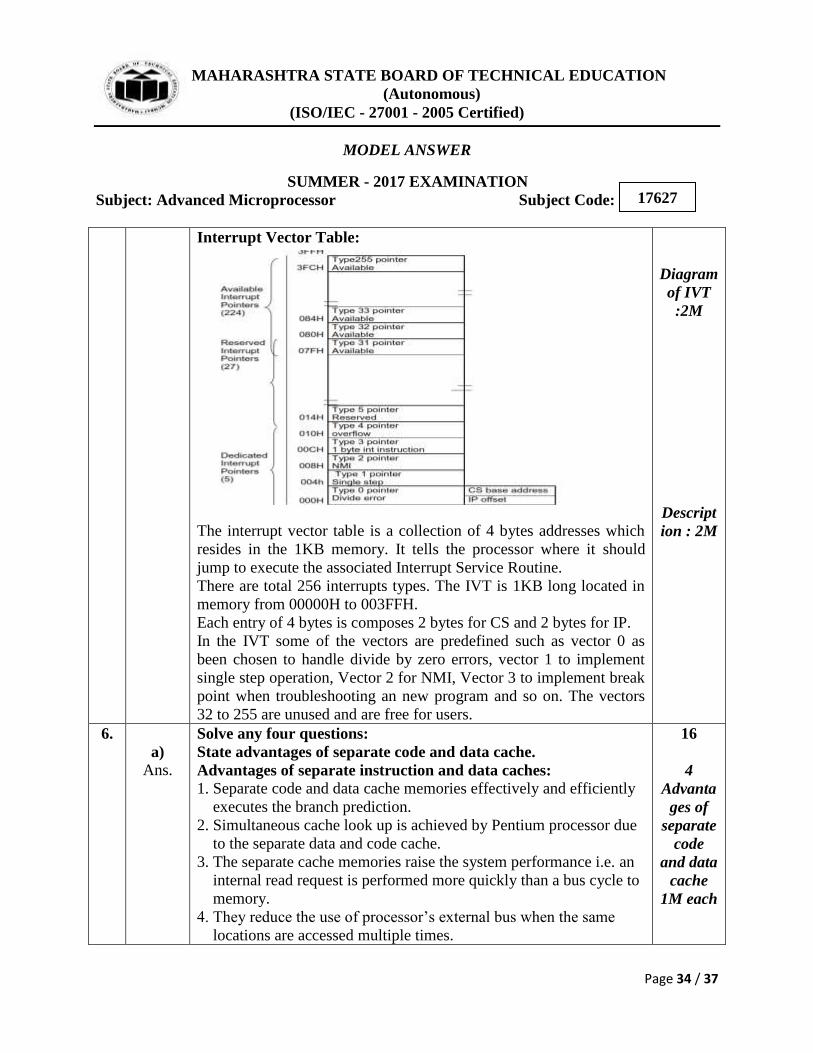
Ans. Draw IVT of x86 processors and explain. 4M
MAHARASHTRA STATE BOARD OF TECHNICAL EDUCATION
(Autonomous)
(ISO/IEC - 27001 - 2005 Certified)
MODEL ANSWER
SUMMER - 2017 EXAMINATION
Subject: Advanced Microprocessor Subject Code:
Page 34 / 37
17627
Interrupt Vector Table:
The interrupt vector table is a collection of 4 bytes addresses which
resides in the 1KB memory. It tells the processor where it should
jump to execute the associated Interrupt Service Routine. There are total 256 interrupts types. The IVT is 1KB long located in
memory from 00000H to 003FFH.
Each entry of 4 bytes is composes 2 bytes for CS and 2 bytes for IP.
In the IVT some of the vectors are predefined such as vector 0 as
been chosen to handle divide by zero errors, vector 1 to implement
single step operation, Vector 2 for NMI, Vector 3 to implement break
point when troubleshooting an new program and so on. The vectors
32 to 255 are unused and are free for users.
Diagram
of IVT
:2M
Descript
ion : 2M
6.
a)
Ans.
Solve any four questions:
State advantages of separate code and data cache.
Advantages of separate instruction and data caches:
1. Separate code and data cache memories effectively and efficiently
executes the branch prediction.
2. Simultaneous cache look up is achieved by Pentium processor due
to the separate data and code cache.
3. The separate cache memories raise the system performance i.e. an
internal read request is performed more quickly than a bus cycle to
memory.
4. They reduce the use of processor’s external bus when the same
locations are accessed multiple times.
16
4
Advanta
ges of
separate
code
and data
cache
1M each

MAHARASHTRA STATE BOARD OF TECHNICAL EDUCATION
(Autonomous)
(ISO/IEC - 27001 - 2005 Certified)
MODEL ANSWER
SUMMER - 2017 EXAMINATION
Subject: Advanced Microprocessor Subject Code:
Page 35 / 37
17627
b)
Ans.
Enlist various file processing functions corresponding to
respective file operations.
(Note: Any other valid functions may be considered)
1. Function 3Ch- Create a File
Creates a new file or shortens an old file to 0 length in preparation
for writing..
Input: AH = 3Ch DS:DX = pointer to an ASCIIZ string
CX = attribute of the file output: AX = error codes if carry flag is set
16-bit handle if carry flag not set
2. Function 3Dh- Open a File
Opens the specified file.
Input: AH = 3Dh
DS:DX = pointer ta an ASCIIZ path name
AL = access Code
output: AX = error codes if carry flag is set
16-bit handle if carry flag not set
3. Function 3Eh- Close a File Handle
Closes the specified file handle.
Input: AH = 3Eh
BX = file handle returned by q3en or create
Output: AX = error code if carry flag is set
none If carry flag not ret
4. Function 3Fh- Read from a File or Device
Transfer a specified number of bytes from a file into a buffer location
Input : AH = 3FH
BX = file handle
DS:DX = buffer address
cx = number of bytes to be read
Output: AX = number of bytes read
error codes if carry flag set
4M
Any two
file
processi
ng
function
s under
INT
21H:
2M each
MAHARASHTRA STATE BOARD OF TECHNICAL EDUCATION
(Autonomous)
(ISO/IEC - 27001 - 2005 Certified)
MODEL ANSWER
SUMMER - 2017 EXAMINATION
Subject: Advanced Microprocessor Subject Code:
Page 36 / 37
17627
c)
Ans.
List advantages of RISC processors.
(Note: Any other valid disadvantages to be considered) Disadvantages of RISC processors :
1. The performance of a RISC processor depends on the code that is
being executed. The processor spends much time waiting for first
instruction result before it proceeds with next subsequent
instruction, when a compiler makes a poor job of scheduling
instruction execution.
2. RISC processors require very fast memory systems to feed
various instructions. Typically, a large memory cache is provided
on the chip in most RISC based systems.
3. Massive pipeline structure counts to stalling of cycles in RISCs.
4. Compiler design for RISC is complex.
4M
4
disadvan
tages of
RISC
processo
rs 1M
each
d)
Ans.
What is hybrid architecture? Which feature of RISC are adopted
in CISC processors to make hybrid convergence? Establish your
answer with example.
Hybrid architecture: State of the art processor technology has
changed significantly since RISC chips were first introduced.
Because a number of advancements are used by both RISC and CISC
processors, the lines between the two architectures have begun to
blur. In fact, the two architectures almost seem to have adopted the
strategies of the other. Because processor speeds have increased,
CISC chips are now able to execute more than one instruction within
a single clock. This also allows CISC chips to make use of pipelining.
With other technological improvements, it is now possible to fit many
more transistors on a single chip.
Features of RISC are adopted in CISC processors to make hybrid
convergence:
1. Branch prediction
2. Pipelining
3. Fixed length instructions
4. More number of registers
Examples:
1. Pentium processors
2. AMD Athalon processors.
4M
Hybrid
architect
ure 1M
Features
adopted
by
CISC: 2
features
2M
Example
1M
e)
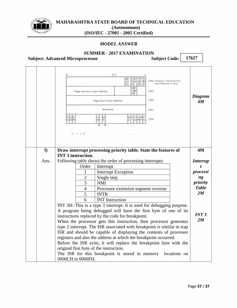
Ans. Draw the structure of pentium control registers.
Diagram of Pentium control registers:
4M
MAHARASHTRA STATE BOARD OF TECHNICAL EDUCATION
(Autonomous)
(ISO/IEC - 27001 - 2005 Certified)
MODEL ANSWER
SUMMER - 2017 EXAMINATION
Subject: Advanced Microprocessor Subject Code:
Page 37 / 37
17627
Diagram
4M
f)
Ans.
Draw interrupt processing priority table. State the features of
INT 3 instruction.
Following table shows the order of processing interrupts:
Order Interrupt
1 Interrupt Exception
2 Single step
3 NMI
4 Processor extension segment overrun
5 INTR
6 INT Instruction
INT 3H: This is a type 3 interrupt. It is used for debugging purpose.
A program being debugged will have the first byte of one of its
instructions replaced by the code for breakpoint.
When the processor gets this instruction, then processor generates
type 2 interrupt. The ISR associated with breakpoint is similar to trap
ISR and should be capable of displaying the contents of processor
registers and also the address at which the breakpoint occurred.
Before the ISR exits, it will replace the breakpoint byte with the
original first byte of the instruction.
The ISR for this breakpoint is stored in memory locations on
0000CH to 0000FH.
4M
Interrup
t
processi
ng
priority
Table
2M
INT 3
2M