model 372xxb vector network analyzer maintenance manual · 2016-03-18 · appendix c — connector...
TRANSCRIPT

P/N: 10410-00182REVISION: D
PRINTED: JUNE 2000COPYRIGHT 1996 ANRITSU CO.
MODEL372XXB
VECTOR NETWORK ANALYZER
MAINTENANCE MANUAL
490 JARVIS DRIVE l MORGAN HILL, CA 95037-2809

WARRANTYThe ANRITSU product(s) listed on the title page is (are) warranted against defects in materials andworkmanship for one year from the date of shipment.ANRITSU’s obligation covers repairing or replacing products which prove to be defective during thewarranty period. Buyers shall prepay transportation charges for equipment returned to ANRITSUfor warranty repairs. Obligation is limited to the original purchaser. ANRITSU is not liable for con-sequential damages.
LIMITATION OF WARRANTYThe foregoing warranty does not apply to ANRITSU connectors that have failed due to normal wear.Also, the warranty does not apply to defects resulting from improper or inadequate maintenance bythe Buyer, unauthorized modification or misuse, or operation outside of the environmental specifi-cations of the product. No other warranty is expressed or implied, and the remedies provided hereinare the Buyer’s sole and exclusive remedies.
TRADEMARK ACKNOWLEDGEMENTSV Connector and K Connector are registered trademarks of ANRITSU Company.ANACAT is a registered trademark of EEsof, Inc.Ink Jet and Think Jet are registered trademarks of Hewlett-Packard Co.MS-DOS is a registered trademark of Microsoft Corporation.
NOTICEANRITSU Company has prepared this manual for use by ANRITSU Company personnel and cus-tomers as a guide for the proper installation, operation and maintenance of ANRITSU Companyequipment and computer programs. The drawings, specifications, and information contained hereinare the property of ANRITSU Company, and any unauthorized use or disclosure of these drawings,specifications, and information is prohibited; they shall not be reproduced, copied, or used in wholeor in part as the basis for manufacture or sale of the equipment or software programs without theprior written consent of ANRITSU Company.

Table of Contents, Narrative
Chapter 1 — General Service InformationThis chapter provides a general description of Series 372XXB Vector Network Analyzer systems, sys-tem serial numbers, and frequency ranges. It explains the level of maintenance covered in this man-ual and the service strategy used throughout this manual. It also contains static-sensitive componenthandling precautions and a list of recommended test equipment.
Chapter 2 — Replaceable PartsThis chapter lists all replaceable subassemblies and components for all 372XXB models. It explainsthe ANRITSUexchange assembly program and provides parts ordering information.
Chapter 3 — Operational TestsThis chapter contains procedures that provide a means of fully testing the 372XXB VNA system forproper operation and signal stability. These tests are intended to be used as a periodic check of theoperational functionality of the 372XXB.
Chapter 4 — Performance Verification ProceduresThis chapter provides detailed procedures for verifying that the performance of the 372XXB meetsminimum performance standards.
Chapter 5 — TroubleshootingThis chapter provides information for troubleshooting Series 372XXB Vector Network Analyzer sys-tems. The troubleshooting procedures contained in this chapter support fault isolation down to a re-placeable subassembly.
Chapter 6 — AdjustmentsThis chapter provides adjustment procedures for all models of Series 372XXB Vector Network Ana-lyzer systems. These procedures are used after replacement or repair of one or more critical subas-semblies, or as indicated by the Performance Verification Procedures contained in Chapter 4.
Chapter 7 — System DescriptionThis chapter provides descriptions of the functional operation of the major assemblies contained inSeries 372XXB Vector Network Analyzer systems. The operation of all major circuit blocks is de-scribed so that the reader may better understand the function of each assembly as part of the overalloperation.
Chapter 8— Removal and Replacement ProceduresThis chapter describes how to gain access to all of the major assemblies and major parts for ¬trouble-shooting and/or replacement.
Appendix A — Diagnostic MenusThis appendix contains descriptions and usage information for the Diagnostic Menus that are avail-able via the front panel Option Menu key.
Appendix B — Error Codes/MessagesThis appendix contains a listing of the Error Codes/Messages. Also included is a description of the in-formation fields that are part of the error messages.
372XXB MM i

Appendix C — Connector Maintenance Check ProceduresThis appendix contains procedures and information needed to perform maintenance checks (includ-ing pin-depth measurements) for the connectors on all ANRITSU supplied Calibration/VerificationKit components, Through-cables, and other associated RF/microwave components.
Appendix D — Performance Specifications
Appendix E — Verification Software Users GuideThis appendix contains the Model 360X/372XXB VNA Performance Verification Software UsersGuide, P/N: 10410-00162. This Software Users Guide explains in detail the procedures to be used forthe installation and operation of the 372XXB VNA Verification Software on your computer/controller.
Index
ii 372XXB MM

Table of Contents
Chapter 1General Information
1-1 SCOPE OF MANUAL · · · · · · · · · · · · · · · · · · · · · · · 1-3
1-2 INTRODUCTION · · · · · · · · · · · · · · · · · · · · · · · · · 1-3
1-3 IDENTIFICATION NUMBER · · · · · · · · · · · · · · · · · · 1-3
1-4 ONLINE MANUAL · · · · · · · · · · · · · · · · · · · · · · · · 1-3
1-5 SYSTEM DESCRIPTION · · · · · · · · · · · · · · · · · · · · · 1-4
1-6 RELATED MANUALS · · · · · · · · · · · · · · · · · · · · · · 1-4
1-7 STANDARD OPTIONS · · · · · · · · · · · · · · · · · · · · · · 1-4
1-8 SERVICE STRATEGY· · · · · · · · · · · · · · · · · · · · · · · 1-5Functional Assembly Level Troubleshooting · · · · · · · · · · · 1-5Internal Hardware Adjustments and Calibrations· · · · · · · · 1-5Internal Service Log · · · · · · · · · · · · · · · · · · · · · · · 1-5System Test/Certification · · · · · · · · · · · · · · · · · · · · · 1-6Preventive Service · · · · · · · · · · · · · · · · · · · · · · · · · 1-6Servicing Specially Modified Instruments · · · · · · · · · · · · 1-6
1-9 SERVICE SUPPORT INFORMATION · · · · · · · · · · · · · · 1-6Technical Support · · · · · · · · · · · · · · · · · · · · · · · · · 1-7Field Service Kits · · · · · · · · · · · · · · · · · · · · · · · · · 1-7Service Software · · · · · · · · · · · · · · · · · · · · · · · · · · 1-7Verification Kits · · · · · · · · · · · · · · · · · · · · · · · · · · 1-8Test Fixtures/ Aids· · · · · · · · · · · · · · · · · · · · · · · · · 1-8Failed Assembly Exchange Program · · · · · · · · · · · · · · · 1-8
1-10 PERFORMANCE SPECIFICATIONS · · · · · · · · · · · · · · 1-9
1-11 SERVICE CENTERS · · · · · · · · · · · · · · · · · · · · · · · 1-9
1-12 STATIC SENSITIVE COMPONENT HANDLING PROCEDURES1-9
1-13 RECOMMENDED TEST EQUIPMENT · · · · · · · · · · · · · 1-9
372XXB MM iii

Chapter 2Replaceable Parts
2-1 INTRODUCTION · · · · · · · · · · · · · · · · · · · · · · · · · 2-3
2-2 EXCHANGE ASSEMBLY PROGRAM · · · · · · · · · · · · · · 2-3
2-3 REPLACEABLE SUBASSEMBLIES AND PARTS · · · · · · · 2-3
2-4 PARTS ORDERING INFORMATION · · · · · · · · · · · · · · 2-4
Chapter 3Operational Tests
3-1 INTRODUCTION · · · · · · · · · · · · · · · · · · · · · · · · · 3-3
3-2 CHECKING THE SERVICE LOG · · · · · · · · · · · · · · · · 3-4
3-3 SELF TEST · · · · · · · · · · · · · · · · · · · · · · · · · · · · 3-5
3-4 PERIPHERALS AND INTERFACES · · · · · · · · · · · · · · 3-6LCD Test · · · · · · · · · · · · · · · · · · · · · · · · · · · · · · 3-6Front Panel Test · · · · · · · · · · · · · · · · · · · · · · · · · · 3-7External Keyboard Interface Test· · · · · · · · · · · · · · · · · 3-7Printer Interface Test · · · · · · · · · · · · · · · · · · · · · · · 3-7GPIB Interface Test · · · · · · · · · · · · · · · · · · · · · · · · 3-9
3-5 SIGNAL PATH · · · · · · · · · · · · · · · · · · · · · · · · · · 3-10
Chapter 4Performance Verification
4-1 INTRODUCTION · · · · · · · · · · · · · · · · · · · · · · · · · 4-3
4-2 CALIBRATION AND MEASUREMENT CONDITIONS · · · · 4-3Standard Conditions · · · · · · · · · · · · · · · · · · · · · · · · 4-3Special Precautions: · · · · · · · · · · · · · · · · · · · · · · · · 4-4
4-3 MEASUREMENT ACCURACY · · · · · · · · · · · · · · · · · · 4-4Verification Software · · · · · · · · · · · · · · · · · · · · · · · 4-4Verification Result Determination · · · · · · · · · · · · · · · · 4-5
4-4 VERIFICATION PROCEDURE· · · · · · · · · · · · · · · · · · 4-5
4-5 MEASURING KEY PARAMETERS · · · · · · · · · · · · · · · 4-6Measurement Environment Considerations · · · · · · · · · · · 4-6Measurement Technique · · · · · · · · · · · · · · · · · · · · · 4-7
iv 372XXB MM
Chapter 5Troubleshooting
5-1 INTRODUCTION · · · · · · · · · · · · · · · · · · · · · · · · · 5-3
5-2 ASSOCIATED INFORMATION · · · · · · · · · · · · · · · · · 5-3
5-3 RECOMMENDED TEST EQUIPMENT · · · · · · · · · · · · · 5-4
5-4 SYSTEM DOES NOT POWER-UP · · · · · · · · · · · · · · · · 5-4Line Source and Interface Checks · · · · · · · · · · · · · · · · 5-4Power Supply Voltages Check· · · · · · · · · · · · · · · · · · · 5-4Power Supply Module Check · · · · · · · · · · · · · · · · · · · 5-6
5-5 SYSTEM DOES NOT BOOT-UP · · · · · · · · · · · · · · · · · 5-7Boot-up Process Sequence · · · · · · · · · · · · · · · · · · · · · 5-7Troubleshooting Boot-up Problems · · · · · · · · · · · · · · · · 5-8Hard Disk Problem 1 · · · · · · · · · · · · · · · · · · · · · · · 5-8Hard Disk Problem 2 · · · · · · · · · · · · · · · · · · · · · · · 5-9Floppy Disk Problems · · · · · · · · · · · · · · · · · · · · · · · 5-9Screen Display Problems · · · · · · · · · · · · · · · · · · · · · 5-10
5-6 SYSTEM PRODUCES ERROR CODE · · · · · · · · · · · · · 5-10Phase Lock Error Codes (6000 Series)· · · · · · · · · · · · · · 5-11Service Log Snap Shot Data · · · · · · · · · · · · · · · · · · · 5-12
5-7 SOURCE/TEST SET/RECEIVER · · · · · · · · · · · · · · · · 5-17Signal Source Phase Lock Loop Assemblies · · · · · · · · · · · 5-17Signal Source/Test Set Module Error Codes · · · · · · · · · · 5-18Isolation Procedures · · · · · · · · · · · · · · · · · · · · · · · 5-19
5-8 PERIPHERALS/ INTERFACE TEST · · · · · · · · · · · · · · 5-21CRT Display Test Failures: · · · · · · · · · · · · · · · · · · · 5-21Front Panel Test Failures: · · · · · · · · · · · · · · · · · · · · 5-22External Keyboard Interface Test Failures:· · · · · · · · · · · 5-22Printer Interface Test Failures: · · · · · · · · · · · · · · · · · 5-22GPIB Interface Test Failures: · · · · · · · · · · · · · · · · · · 5-22
5-9 MEASUREMENTS IN QUESTION · · · · · · · · · · · · · · · 5-22Measurement Conditions Check List · · · · · · · · · · · · · · 5-23
Chapter 6Adjustments
6-1 INTRODUCTION · · · · · · · · · · · · · · · · · · · · · · · · · 6-3
6-2 LO1 CALIBRATION· · · · · · · · · · · · · · · · · · · · · · · · 6-3Calibration Procedure · · · · · · · · · · · · · · · · · · · · · · · 6-3Post Calibration Actions· · · · · · · · · · · · · · · · · · · · · · 6-4
372XXB MM v

6-3 LO 2 CALIBRATION · · · · · · · · · · · · · · · · · · · · · · · 6-4Calibration Procedure · · · · · · · · · · · · · · · · · · · · · · · 6-4Post Calibration Actions· · · · · · · · · · · · · · · · · · · · · · 6-5
6-4 FREQUENCY CALIBRATION · · · · · · · · · · · · · · · · · · 6-5Calibration Procedure · · · · · · · · · · · · · · · · · · · · · · · 6-6Post Calibration Actions· · · · · · · · · · · · · · · · · · · · · · 6-7
6-5 RF POWER/ALC CALIBRATION· · · · · · · · · · · · · · · · · 6-8Calibration Procedure · · · · · · · · · · · · · · · · · · · · · · · 6-9Post Calibration Actions · · · · · · · · · · · · · · · · · · · · · 6-10
6-6 SOURCE LOCK THRESHOLD · · · · · · · · · · · · · · · · · 6-11Calibration Procedure · · · · · · · · · · · · · · · · · · · · · · 6-11Post Calibration Actions · · · · · · · · · · · · · · · · · · · · · 6-12
6-7 A8 ADJUSTMENT · · · · · · · · · · · · · · · · · · · · · · · · 6-12Calibration Procedure · · · · · · · · · · · · · · · · · · · · · · 6-13
6-8 A21A2 ADJUSTMENT · · · · · · · · · · · · · · · · · · · · · 6-13Calibration Procedure · · · · · · · · · · · · · · · · · · · · · · 6-13
Chapter 7System Description
7-1 INTRODUCTION · · · · · · · · · · · · · · · · · · · · · · · · · 7-3
7-2 SYSTEM OVERVIEW · · · · · · · · · · · · · · · · · · · · · · · 7-3
7-3 ANALOG SUBSYSTEM ASSEMBLIES · · · · · · · · · · · · · 7-7Signal Source Module · · · · · · · · · · · · · · · · · · · · · · · 7-7Test Set Module · · · · · · · · · · · · · · · · · · · · · · · · · · 7-8A7 PCB, 10 MHz Timebase· · · · · · · · · · · · · · · · · · · 7-9Receiver Module · · · · · · · · · · · · · · · · · · · · · · · · · 7-10A8, Source Lock/ Signal Separation and Control PCB · · · · · 7-11IF Section · · · · · · · · · · · · · · · · · · · · · · · · · · · · · 7-11A7 PCB, LO3 · · · · · · · · · · · · · · · · · · · · · · · · · · 7-12A5 A/D Converter PCB · · · · · · · · · · · · · · · · · · · · · · 7-12
7-4 DIGITAL SUBSYSTEM ASSEMBLIES· · · · · · · · · · · · · 7-13A9 Main Processor PCB Assembly· · · · · · · · · · · · · · · · 7-13A13 I/O Interface #1 PCB Assembly · · · · · · · · · · · · · · · 7-15A14 I/O Interface #2 PCB Assembly · · · · · · · · · · · · · · · 7-15A15 Graphics Processor PCB Assembly · · · · · · · · · · · · · 7-16A16 Hard Disk PCB Assembly · · · · · · · · · · · · · · · · · · 7-16Floppy Disk Drive Assembly · · · · · · · · · · · · · · · · · · · 7-16A24 VME Bus Terminator PCB · · · · · · · · · · · · · · · · · 7-16
7-5 MAIN CHASSIS ASSEMBLIES · · · · · · · · · · · · · · · · · 7-16A17 System Motherboard Assembly · · · · · · · · · · · · · · · 7-16
vi 372XXB MM

Front Panel Assembly · · · · · · · · · · · · · · · · · · · · · · 7-16Rear Panel Assembly · · · · · · · · · · · · · · · · · · · · · · · 7-17A18 Rear Panel Interface PCB· · · · · · · · · · · · · · · · · · 7-17Power Supply Module · · · · · · · · · · · · · · · · · · · · · · 7-18Internal VGA Monitor · · · · · · · · · · · · · · · · · · · · · · 7-19
Chapter 8Remove and ReplaceProcedures
8-1 INTRODUCTION · · · · · · · · · · · · · · · · · · · · · · · · · 8-3
8-2 EQUIPMENT REQUIRED · · · · · · · · · · · · · · · · · · · · 8-3
8-3 COVERS · · · · · · · · · · · · · · · · · · · · · · · · · · · · · · 8-4
8-4 A1–A9/A13–A16 PCBS · · · · · · · · · · · · · · · · · · · · · · 8-6A1 – A9 PCBs · · · · · · · · · · · · · · · · · · · · · · · · · · · 8-6A13 – A16 PCB’s · · · · · · · · · · · · · · · · · · · · · · · · · · 8-6
8-5 A9 PCB BBRAM CHIP · · · · · · · · · · · · · · · · · · · · · · 8-6
8-6 A9 PCB SRAM BATTERY· · · · · · · · · · · · · · · · · · · · 8-10
8-7 A24 VME PCB · · · · · · · · · · · · · · · · · · · · · · · · · · 8-12
8-8 FRONT PANEL ASSEMBLY · · · · · · · · · · · · · · · · · · 8-13
8-9 VGA MONITOR · · · · · · · · · · · · · · · · · · · · · · · · · 8-14
8-10 LIQUID CRYSTAL DISPLAY (LCD) · · · · · · · · · · · · · · 8-16
8-11 LCD BACKLIGHT LAMP · · · · · · · · · · · · · · · · · · · · 8-17
8-12 FLOPPY DISK DRIVE · · · · · · · · · · · · · · · · · · · · · · 8-17
8-13 REAR PANEL ASSEMBLY · · · · · · · · · · · · · · · · · · · 8-19
8-14 FAN ASSEMBLY· · · · · · · · · · · · · · · · · · · · · · · · · 8-21
8-15 POWER SUPPLY MODULE· · · · · · · · · · · · · · · · · · · 8-21
8-16 A18 REAR PANEL PCB · · · · · · · · · · · · · · · · · · · · · 8-22
8-17 TEST SET MODULE ASSEMBLIES · · · · · · · · · · · · · · 8-25Transfer Switch· · · · · · · · · · · · · · · · · · · · · · · · · · 8-25Input Coupler(s)/ Low Freq Bridge(s) · · · · · · · · · · · · · · 8-26Power Amplifier · · · · · · · · · · · · · · · · · · · · · · · · · 8-26Buffer Amplifier/ Sampler(A31) · · · · · · · · · · · · · · · · · 8-27
372XXB MM vii

Switched Doubler Module Assembly· · · · · · · · · · · · · · · 8-28
8-18 SIGNAL SOURCE MODULES · · · · · · · · · · · · · · · · · 8-29Removal of Signal Source Module · · · · · · · · · · · · · · · · 8-29A21A2 Source Control PCB · · · · · · · · · · · · · · · · · · · 8-31A21A1 Source YIG Bias Control PCB · · · · · · · · · · · · · · 8-32Switched FilterAssembly · · · · · · · · · · · · · · · · · · · · · · · · · · · · · 8-33Down Converter Assembly · · · · · · · · · · · · · · · · · · · · 8-33YIG Oscillator Assembly · · · · · · · · · · · · · · · · · · · · · 8-34
Appendix ADiagnostics Menus
A-1 INTRODUCTION · · · · · · · · · · · · · · · · · · · · · · · · · A-3
A-2 DIAGNOSTICS MENUS · · · · · · · · · · · · · · · · · · · · · A-3Start Self Test · · · · · · · · · · · · · · · · · · · · · · · · · · · A-3Read Service Log · · · · · · · · · · · · · · · · · · · · · · · · · A-3Installed Options · · · · · · · · · · · · · · · · · · · · · · · · · A-4Peripheral Tests · · · · · · · · · · · · · · · · · · · · · · · · · · A-4Troubleshooting · · · · · · · · · · · · · · · · · · · · · · · · · · A-4H/W Calibrations · · · · · · · · · · · · · · · · · · · · · · · · · A-5
Appendix BError Messages
B-1 INTRODUCTION · · · · · · · · · · · · · · · · · · · · · · · · · B-3
B-2 OPERATIONAL ERROR MESSAGES · · · · · · · · · · · · · · B-3
B-3 DISK RELATED ERROR MESSAGES· · · · · · · · · · · · · · B-3
B-4 GPIB RELATED ERROR MESSAGES· · · · · · · · · · · · · · B-3
B-5 SERVICE LOG ERROR MESSAGES · · · · · · · · · · · · · · B-30000 - 0099 · · · · · · · · · · · · · · · · · · · · · · · · · · · · B-30100 - 3999 · · · · · · · · · · · · · · · · · · · · · · · · · · · · B-34000 - 4999 · · · · · · · · · · · · · · · · · · · · · · · · · · · · B-45000 - 5999 · · · · · · · · · · · · · · · · · · · · · · · · · · · · B-46000 - 6999 · · · · · · · · · · · · · · · · · · · · · · · · · · · · B-47000 - 7999 · · · · · · · · · · · · · · · · · · · · · · · · · · · · B-48000 - 8999 · · · · · · · · · · · · · · · · · · · · · · · · · · · · B-4
Appendix CConnector MaintenanceCheck Procedures
C-1 INTRODUCTION · · · · · · · · · · · · · · · · · · · · · · · · · C-3
viii 372XXB MM

C-2 PRECAUTIONS · · · · · · · · · · · · · · · · · · · · · · · · · C-3Pin-Depth Tolerance · · · · · · · · · · · · · · · · · · · · · · · C-4Avoid Over Torquing Connectors · · · · · · · · · · · · · · · · C-4Teflon Tuning Washers · · · · · · · · · · · · · · · · · · · · · · C-4Avoid Mechanical Shock · · · · · · · · · · · · · · · · · · · · · C-4Keep Connectors Clean · · · · · · · · · · · · · · · · · · · · · · C-5VisualInspection · · · · · · · · · · · · · · · · · · · · · · · · · · · · · C-5
C-3 REPAIR/ MAINTENANCE · · · · · · · · · · · · · · · · · · · C-5
Appendix DPerformance Specifications
Appendix EPerformance VerificationSoftware User’s Guide
SubjectIndex
372XXB MM ix

x 372XXB MM

Table of Contents1-1 SCOPE OF MANUAL · · · · · · · · · · · · · · · · · · · · · · · 1-3
1-2 INTRODUCTION · · · · · · · · · · · · · · · · · · · · · · · · · 1-3
1-3 IDENTIFICATION NUMBER · · · · · · · · · · · · · · · · · · 1-3
1-4 ONLINE MANUAL · · · · · · · · · · · · · · · · · · · · · · · · 1-3
1-5 SYSTEM DESCRIPTION · · · · · · · · · · · · · · · · · · · · · 1-4
1-6 RELATED MANUALS · · · · · · · · · · · · · · · · · · · · · · 1-4
1-7 STANDARD OPTIONS · · · · · · · · · · · · · · · · · · · · · · 1-4
1-8 SERVICE STRATEGY· · · · · · · · · · · · · · · · · · · · · · · 1-5Functional Assembly Level Troubleshooting · · · · · · · · · · · 1-5Internal Hardware Adjustments and Calibrations· · · · · · · · 1-5Internal Service Log · · · · · · · · · · · · · · · · · · · · · · · 1-5System Test/Certification · · · · · · · · · · · · · · · · · · · · · 1-6Preventive Service · · · · · · · · · · · · · · · · · · · · · · · · · 1-6Servicing Specially Modified Instruments · · · · · · · · · · · · 1-6
1-9 SERVICE SUPPORT INFORMATION · · · · · · · · · · · · · · 1-6Technical Support · · · · · · · · · · · · · · · · · · · · · · · · · 1-7Field Service Kits · · · · · · · · · · · · · · · · · · · · · · · · · 1-7Service Software · · · · · · · · · · · · · · · · · · · · · · · · · · 1-7Verification Kits · · · · · · · · · · · · · · · · · · · · · · · · · · 1-8Test Fixtures/ Aids· · · · · · · · · · · · · · · · · · · · · · · · · 1-8Failed Assembly Exchange Program · · · · · · · · · · · · · · · 1-8
1-10 RECOMMENDED TEST EQUIPMENT · · · · · · · · · · · · · 1-9
1-11 STATIC SENSITIVE COMPONENT HANDLINGPROCEDURES · · · · · · · · · · · · · · · · · · · · · · · · · · 1-11
1-12 SERVICE CENTERS· · · · · · · · · · · · · · · · · · · · · · · 1-11
1-13 PERFORMANCE SPECIFICATIONS· · · · · · · · · · · · · · 1-11
Chapter 1General Information
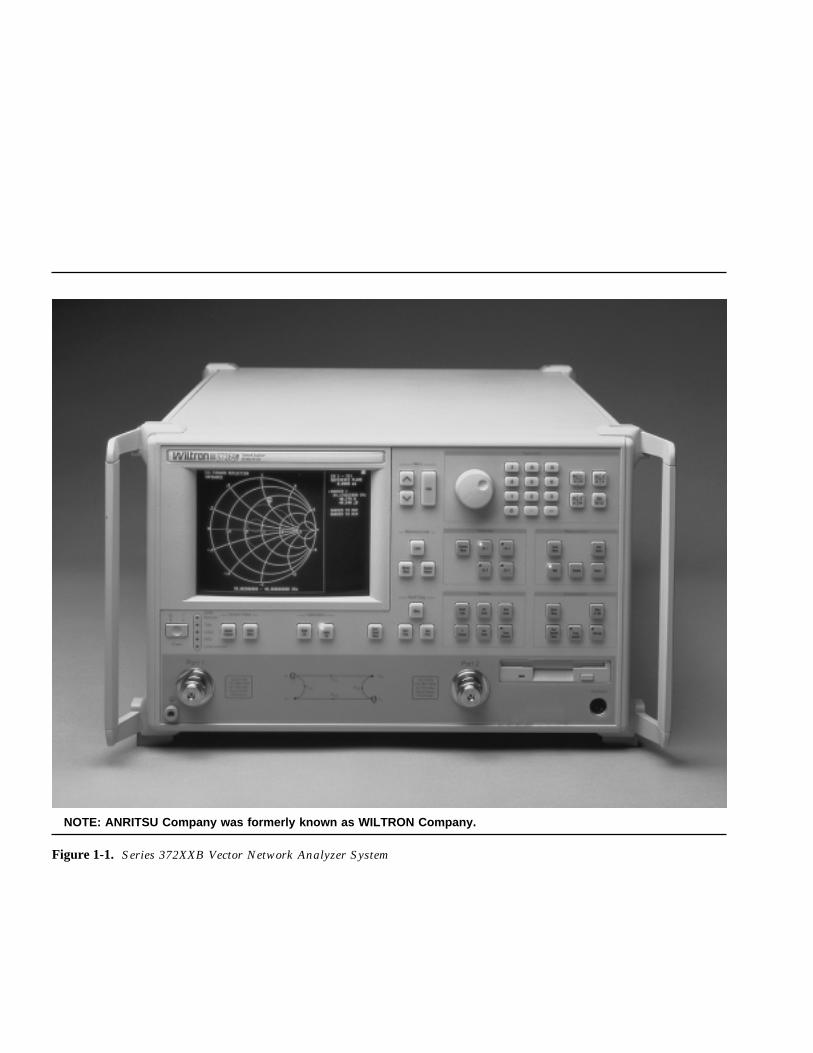
Figure 1-1. Series 372XXB Vector Network Analyzer System
NOTE: ANRITSU Company was formerly known as WILTRON Company.

1-1 SCOPE OF MANUAL This manual provides general service and preventive maintenance in-formation for the ANRITSU 372XXB family of Vector NetworkAnalyzer (VNA) systems. It contains procedures for:
� Testing the instrument for proper operation.
� Verifying measurement accuracy and traceability to National In-stitute of Standards and Technology (NIST).
� Troubleshooting a failed instrument to the exchange subassem-bly level or the subsystem requiring adjustment.
� Adjusting instrument internal sub-systems.
� Locating and replacing failed parts.
Throughout this manual, the terms “372XXB” and “372XXB VNA”will be used interchangeably to refer to all Series 37200B NetworkAnalyzer system models, unless otherwise noted.
1-2 INTRODUCTION This chapter of the manual provides a general description of 372XXBVNA systems, system serial numbers, frequency ranges, and relatedmanuals. Also included is information about the level of maintenance cov-ered in this manual, service strategy, available service facilities, andstatic-sensitive component handling precautions. A list of recommendedtest equipment is also provided.
1-3 IDENTIFICATIONNUMBER
All ANRITSU instruments are assigned a six-digit ID number, such as“401001”. This number appears on a decal affixed to the rear panel.Please use this identification number during any correspondence withANRITSU Customer Service about this instrument.
1-4 ONLINE MANUAL This manual is available on CD ROM as an Adobe Acrobat™ (*.pdf)file. The file can be viewed using Acrobat Reader™, a free programthat is also available on the CD ROM. This file is “linked” such thatthe viewer can choose a topic to view from the displayed “bookmark”list and “jump” to the manual page on which the topic resides. Thetext can also be word-searched. Contact ANRITSU Customer Servicefor price and availability.
372XXB MM 1-3
Chapter 1General Information
1-5 SYSTEM DESCRIPTION The 372XXB Analyzers are microprocessor controlled Vector NetworkAnalyzers. Each is a single-instrument system that contains a built-insignal source, a test set, and an analyzer subsystem. A typical model(37269B) is shown in Figure 1-1. These analyzers are produced in fivemodels that cover a range of from 22.5 MHz to 65 GHz. The table at leftlists the frequencies for each model.
1-6 RELATED MANUALS The 372XXB Vector Network Analyzer Operation Manual (10410-00180)describes the front panel operation for all 372XXB models. It also con-tains general information, specifications, and Performance Verificationprocedures for all models.
The 37XXX Series Vector Network Analyzer Programming Manual(10410-00200) describes all 372XXB GPIB commands and providesprogramming information for operation of the 372XXB remotely viathe IEEE-488 General Purpose Interface Bus. Included at the rear ofthis manual is the 37XXX Series Vector Network Analyzer GPIBQuick Reference Guide (10410-00201).
Model 360X/372XXB VNA Performance Verification Software UsersGuide, P/N: 10410-00162 (located in Appendix E at the rear of thismanual). This Software Users Guide explains in detail the proceduresto be used for the installation and operation of the 372XXB VNA Veri-fication Software on your computer/controller.
1-7 STANDARD OPTIONS The standard 372XXB VNA options and their respective Upgrade Kitpart numbers are:
Option* Description Upgrade Kit
Opt 1 Rack Mount with slides ND39486
Opt 1A Rack Mount ND40916
Opt 2A Time Domain (Microwave Units) ND39477
Opt 2B Time Domain (RF Units) ND40914
Opt 10A High Stability Ovenized Time Base ND45045
* All options listed can be installed at ANRITSU Service Centers
SYSTEM DESCRIPTION GENERAL INFORMATION
1-4 372XXB MM
Model Freq Range
37217B 22.5 MHz to 8.6 GHz
37225B 40.0 MHz to 13.5 GHz
37247B 40.0 MHz to 20.0 GHz
37269B 40.0 MHz to 40.0 GHz
37297B 40.0 MHz to 65.0 GHz
372XXB Model Frequencies

1-8 SERVICE STRATEGY This paragraph provides an overview of the 372XXB VNA service strat-egy and available service facilities. It also provides references to the infor-mation in various locations in this manual needed to accomplish the ser-vice functions required for the 372XXB VNA.
Appendices - Refer to the Appendices at the rear of this manual for de-tailed descriptions of the following:
� Diagnostics Menus and GPIB Commands.
� Error Messages.
� System Block Diagrams.
� Parts Locator Diagrams.
Functional AssemblyLevel Troubleshooting
The 372XXB modular design, extensive built-in diagnostics, and auto-mated service tools are designed to support fast exchange of functional as-sembly level repairs.
Failed assemblies are not field repairable. Once an assembly is foundto be faulty, it should be returned to an authorized ANRITSU ServiceCenter for exchange. Refer to the description of the Exchange Assem-bly Program in Chapter 2, Replaceable Parts.
The procedures for troubleshooting a failed 372XXB VNA are de-scribed in this manual in Chapter 5, Troubleshooting.
Internal HardwareAdjustments and Cal-
ibrations
There are five automated internal hardware field calibrations. Two ofthem are used to characterize the 372XXB frequency and power genera-tion sub-systems. These calibrations insure fast, consistent phase lock ofsystem frequencies and proper compensation, leveling, and flatness ofsystem power at the front panel test ports.
To conduct these calibrations, you need only connect the appropriatetest equipment (counter or power meter) to the 372XXB and initiatethe calibration. The 372XXB will control itself and the externally con-nected test equipment to perform measurements and store calibrationconstants in its internal battery backed RAM (BBRAM).
The procedures for adjusting the 372XXB VNA are described in thismanual in Chapter 6, Adjustments.
Internal Service Log The 372XXB continuously monitors itself for proper operation. Should afailure occur, it notifies the user via a failure message on the displayscreen. (In remote-only operation, it also sets the GPIB Status Byte, ifenabled.) It also writes the error message along with some data pertinentto the failure to an internal service log stored in battery backed memory.
The service log can be checked at any time to view (without erasing)all error messages that were written into it. It is capable of storing
GENERAL INFORMATION SERVICE STRATEGY
372XXB MM 1-5

more than 30 pages of service messages and data. The 372XXB willautomatically remove the oldest errors first to make room for new er-rors, if necessary. To check the contents of the service log, use the pro-cedure described in Chapter 3, Operational Tests.
NOTEA printed or disk file copy of the Service Log (with the fail-ure in question) must be made available to ANRITSUwhen exchanging a failed assembly, or when requestingservice support. Refer to Chapter 2, Replaceable Parts, forfurther information.
SystemTest/Certification
Quick operational checkout of the system may be accomplished by thesystem user or for incoming inspection purposes using the “OperationalCheckout” chapter in the 372XXB Operations Manual. Those proceduresare useful in quickly verifying that the instrument’s primary measure-ment functions are operational and stable.
Full operational testing of the system is detailed in Chapter 3, Opera-tional Tests. These tests should be performed annually, or more oftendepending on system use.
Verification of the system’s measurement accuracy and other key per-formance parameters may be done using the procedures in Chapter 4,Performance Verification. This should be performed annually, or moreoften depending on system use.
Preventive Service The 372XXB A9 Processor PCB contains a battery backed memory/realtime clock chip (BBRAM) and a static memory (SRAM) backup battery.These have a finite life span and should be replaced periodically per theprocedures in Chapter 8, Removal and Replacement Procedures.
The BBRAM chip has a rated life span of 4 years. The SRAM backupbattery has a worst case elapsed time for SRAM battery protection of200 days. The SRAM battery life span will vary according to how thesystem is used; that is, how often the system is powered off for ex-tended periods of time.
Servicing SpeciallyModified Instruments
Instruments with customer requested special modifications performed byANRITSU will have an identifying Specials Modification number printedon the rear panel. This number will be preceded with the letters SM, i.e.,SM1234 is special modification number 1234.
Special instruments may have service requirements different fromthose specified in this manual. Contact your local Service Center if youneed more information when servicing such instruments.
1-9 SERVICE SUPPORTINFORMATION
The following paragraphs briefly describe the various service support ser-vices and aids available to you to help you maintain your 372XXB.
SERVICE SUPPORT INFORMATION GENERAL INFORMATION
1-6 372XXB MM

Technical Support Technical service support is available by contacting any ANRITSUWorldwide Service Center (refer to paragraph 1-11). Or, service supportmay be obtained directly from the factory by contacting:
ANRITSU CompanyATTN: Customer Service490 Jarvis DriveMorgan Hill, CA 95037-2809
Telephone: (408)-778-2000FAX: (408)-778-0239
If servicing or repairing your own system and you need technical sup-port, you will need to FAX or mail a printout of the items listed belowto the ANRITSU Customer Support Engineer:
� Measurement data in question� “Operational Tests” results� System state (from UTILITY menu)� Service Log (from DIAGNOSTICS menu)
Field Service Kits The field service kit listed below is available through your local ANRITSUSales or Service Center:
ND37200A-2, Field Service KitThis kit provides for automated field test and performance verificationof the 372XXB. It is packaged in a hardened rolling case that also hasspace for two, user supplied, verification and calibration kits and otheraccessories.
The ND37200A-2, Field Service Kit is comprised of all major subas-semblies of all models 40 Ghz and below high-end frequency.
ND53269, Field Service KitThis kit provides for automated field test and performance verificationof the 372XXB 65 GHz models (37397A). It supplements kitND37200A-2.
Service Software The service software listed below is contained on the diskette located atthe rear of this manual:
ANRITSU 37XXX Test Software (2300-178).This software contains a series of automated tests designed to insurethe 372XXB signal paths are functioning properly and capable of sup-porting stable calibrations and measurements. See Operational TestsChapter for details.
ANRITSU 37XXX Performance Verification Software (2300-237).This software is used to verify the 372XXB published measurement ac-curacy and traceability to the U.S. National Institute of Standards andTechnology (NIST). See Chapter 4, Performance Verification, for de-tails.
GENERAL INFORMATION SERVICE SUPPORT INFORMATION
372XXB MM 1-7

Verification Kits The ANRITSU Verification Kits listed below are used in conjunction withthe 37XXX Performance Verification Software (above). See Chapter 4,Performance Verification, for further information.
N Verification Kit (Model 3663)Contains precision N Connector components that are traceable to theNIST. Use for Model 37217B and below, with Option 7N or 7NF.
GPC-3.5 Verification Kit (Model 3666)Contains precision Connector components that are traceable to theNIST. Use for Model 37247B and below with Option 7S.
GPC-7 Verification Kit (Model 3667)Contains precision GPC-7 Connector components whith characteristicsthat are traceable to the NIST.Use for Models 37217B and below with Option 7A.
K Verification Kit (Model 3668)Contains precision K Connector components that are traceable to theNIST.
V Verification Kit (Model 3669B)Contains precision V Connector components that are traceable to theNIST.
Test Fixtures/ Aids The test fixtures and test aids listed below are available through your lo-cal ANRITSU Sales or Service Center:
Rear Panel Printer Port Test Fixture (B39553).This test fixture is used to check out digital printer interface circuitson the rear panel assembly.
GPIB Cable (2100-2).This cable is used to check out digital GPIB interface circuits on therear panel assembly.
Failed AssemblyExchange Program
The exchange program allows a customer to quickly exchange a failedsubassembly for a factory refurbished, fully system-tested and unit that isunder warranty. This results in significant time and price savings as com-pared with ordering a new assembly.
Refer to Chapter 2, Replaceable Parts, for a complete list of exchange-able assemblies for all Series 372XXB models.
NOTEWhen sending a failed assembly to the factory for ex-change, a copy of the Service Log must always accom-pany the failed assembly. Refer to Chapter 2, ReplaceableParts, for further information.
SERVICE SUPPORT INFORMATION GENERAL INFORMATION
1-8 372XXB MM

1-10 PERFORMANCESPECIFICATIONS
The performance specifications for all Series 372XXB models are con-tained in the Technical Data Sheets that are located in Appendix D,Performance Specifications.
1-11 SERVICE CENTERS ANRITSU Company offers a full range of repair and calibration servicesat fully staffed and equipped service centers throughout the world. Table2-1, located on page 2-4, lists all ANRITSU services centers.
1-12 STATIC SENSITIVECOMPONENTHANDLINGPROCEDURES
The 372XXB contains components that can be damaged by static electric-ity. Figure 1-2 illustrates the precautions that should be followed whenhandling static-sensitive subassemblies and components. If followed,these precautions will minimize the possibilities of static-shock damage tothese items.
1-13 RECOMMENDED TESTEQUIPMENT
Table 1-1 lists the recommended test equipment to be used for all mainte-nance activities for all Series 372XXB models. Note the “Use” codeslisted in the right hand column of the table. These codes list the appli-cable maintenance activities for the equipment listed.
GENERAL INFORMATION PERFORMANCE SPECIFICATIONS
372XXB MM 1-9

RECOMMENDED TEST EQUIPMENT GENERAL INFORMATION
1-10 372XXB MM
INSTRUMENT CRITICALSPECIFICATION
RECOMMENDEDMANUFACTURER/MODEL
USE**
Computer/Controller Equipped with National Instruments GPIB In-terface Adapter, w/Driver Software V2.1 orlater
ANRITSU 360CC or 360CC-2, witha PCII/IIA, or, ANRITSU 360CC-3and RS-232/GPIB-US (or -UK/ -EU)
O, P
Test Software ANRITSU 2300-178 O
Floppy Disk Formatted, IBM PC format DS/HD 1.44 Mbyte A
GPIB Cable ANRITSU 2100-2, or equivalent O, P,A
RF/Microwave Cable DC to 65 Ghz, K or V type connectors.Length, 2 ft.
ANRITSU 3670K50-2 or 3670V50-2 P, A
BNC Cable Length, 4 ft., 2 each Any O
Printer Port TestFixture
ANRITSU B39553 O
Thru Line For models 37217B and belowFor models 37225B and above:
ANRITSU 3670A50-2, 3671A50-2ANRITSU 3670K50-2, 3671K50-2
O, P
Calibration Kit For models 37217B and below, with Opt 7A:For models 37217B and below, with Opt 7Nor 7NF:For models 37225B and above:For models 37247B and below, with Opt 7S:For model 37297B
ANRITSU 3651-1*ANRITSU 3653
ANRITSU 3652-1*ANRITSU 3650-1*ANRITSU 3654B
O, P
Performance Verifica-tion Software
ANRITSU 2300-237 P
Connector VerificationKit
For models 37217B and below w/Opt 7A:For models 37217B and below, with Opt 7Nor 7NF:For models 37225B and above:For models 37247B and below, with Opt 7S:
For model 37297B
ANRITSU 3667
ANRITSU 3663
ANRITSU 3668ANRITSU 3666
ANRITSU 3669B
P
* Calibration Kit sliding load (Option {-1}), required for Performance Verification only.
** USE CODES:A Adjustment / Internal Hardware CalibrationO Operational TestingP Performance VerificationT Troubleshooting
Table 1-1. Recommended Test Equipment (1 of 2)

GENERAL INFORMATION RECOMMENDED TEST EQUIPMENT
372XXB MM 1-11
INSTRUMENT CRITICALSPECIFICATION
RECOMMENDEDMANUFACTURER/MODEL
USE**
Assurance Air Line For models 37217B and below w/Opt 7A:For models 37217B and below w/Opt 7N:For models 37217B and below w/Opt 7NF:For models 37225B and above:For models 37247B and below w/Opt 7S:
ANRITSU 18A50ANRITSU 18NF50ANRITSU 18N50ANRITSU T1519ANRITSU T1147-2
P
Offset Termination For models 37217B and below w/Opt 7A, 7N,7NF:All other models having K connectors
ANRITSU 29A50-20
ANRITSU 29KF50-15
P
Frequency Counter Frequency: 0.1 to 26.5 GHzInput Impedance: 50W
EIP Microwave, Inc., Model 578B P, A
Digital Multimeter Resolution: 412 digits
DC Accuracy: 0.1 %AC Accuracy: 0.1 %
Any T
Oscilloscope Bandwidth: DC to 100 MHzSensitivity: 2 mVHoriz. Sensitivity: 50 ns/division
Tektronix, Inc.Model 2445
T
Power Meter 1, with: Power Range: –30 to +20 dBm(1 mW to 100 mW)
Other: GPIB controllable
HP 437B with Option 22 (GPIB) P, A
Power Sensor 1or:
Power Meter 2, with:Power Sensor 2
Frequency Range: 0.05 to 50 GHzPower Range: –70 to +47 dBm
(100 pW to 50 W)Other: GPIB controllableFrequency Range: 0.01 to 40 GHz
HP 8487A
Gigatronics 8541 or 8542Gigatronics 80304A
P, A
Power Meter and PowerSensor
Frequency Range: to 65 GHz Anritsu Model ML24xxA Power Meterand MA2474A (40 GHz and below)and Model SC6230 (to 65 GHz)Power Sensors
Gauging Set GPC-7 Gauging SetK Connector Gauging Set
ANRITSU 01-161ANRITSU 01-162
O, T
** USE CODES:A Adjustment / Internal Hardware CalibrationO Operational TestingP Performance VerificationT Troubleshooting
Table 1-1. Recommended Test Equipment (2 of 2)

COMPONENT HANDLING GENERAL INFORMATION
1-12 372XXB MM
1. Do not touch exposed contactson any static sensitivecomponent.
2. Do not slide static sensitivecomponent across any surface.
3. Do not handle static sensitivecomponents in areas where thefloor or work surface covering iscapable of generating a staticcharge.
4. Wear a static-dischargewristband when working withstatic sensitive components.
5. Label all static sensitive devices. 6. Keep component leads shortedtogether whenever possible.
7. Handle PCBs only by theiredges. Do not handle by the edgeconnectors.
8. Lift & handle solid state devicesby their bodies – never by theirleads.
9. Transport and store PCBs andother static sensitive devices instatic-shielded containers.
10. ADDITIONAL PRECAUTIONS:• Keep workspaces clean and free of any objects capable of holding or storing a static charge.• Connect soldering tools to an earth ground.• Use only special anti-static suction or wick-type desoldering tools.
Figure 1-2. Static Sensitive Component Handling Procedures

Table of Contents2-1 INTRODUCTION · · · · · · · · · · · · · · · · · · · · · · · · · 2-3
2-2 EXCHANGE ASSEMBLY PROGRAM · · · · · · · · · · · · · · 2-3
2-3 REPLACEABLE SUBASSEMBLIES AND PARTS · · · · · · · 2-3
2-4 PARTS ORDERING INFORMATION · · · · · · · · · · · · · · 2-4
Chapter 2Replaceable Parts


Chapter 2Replaceable Parts
2-1 INTRODUCTION This chapter provides replaceable parts information for all 372XXBmodels. The major replaceable 372XXB assemblies and parts arelisted in Tables 2-2 through 2-7. The locations of these assem-blies/parts are shown in Figures 2-1 through 2-3.
2-2 EXCHANGE ASSEMBLYPROGRAM
ANRITSU maintains a module exchange program for selected subassem-blies. If a malfunction occurs in one of these subassemblies, the defectiveitem can be exchanged. Upon receiving your request, ANRITSU will shipthe exchange subassembly to you, typically within 24 hours. You thenhave 45 days in which to return the defective item. All exchange subas-semblies or RF assemblies are warranted for 90 days from the date ofshipment, or for the balance of the original equipment warranty, which-ever is longer.
NOTEWhen sending a failed assembly to the factory for ex-change, a copy of the Service Log must always accom-pany the failed assembly. This copy may be a printout, ora saved disk copy. Due to the importance of the service loginformation to the ANRITSU factory Service Engineers,the exchange prices are only valid if the service log data isincluded with the failed assembly.
Please have the exact model number and serial number of your unitavailable when requesting this service, as the information about yourunit is filed according to the instrument’s model and serial number.For more information about the program, contact your local sales rep-resentative or call ANRITSU Customer Service direct (refer to para-graph 2-4.
2-3 REPLACEABLESUBASSEMBLIES ANDPARTS
Tables 2-2 through 2-5, (starting page 2-5) list the major replaceable sub-assemblies and parts for the 372XXB. These assemblies/parts are pres-ently covered by the ANRITSU exchange assembly program. Table 2-6(page 2-6) lists disposable parts for the 372XXB, and Table 2-7 lists fac-tory-repairable parts for the 372XXB. (The parts listed in Tables 2-6 and2-7 are not presently on the exchange assembly program.)
NOTEThe 372XXB A17 Motherboard PCB Assembly is not afield-replaceable item.
372XXB MM 2-3

2-4 PARTS ORDERINGINFORMATION
All parts listed in Tables 2-2 through 2- 7 may be ordered from your localANRITSU service center (Table 2-1). Or, they may be ordered directlyfrom the factory at the following address:
ANRITSU CompanyATTN: Customer Service490 Jarvis DriveMorgan Hill, CA 95037-2809
Telephone: (408)-778-2000FAX: (408)-778-0239
PARTS ORDERING INFORMATION GENERAL INFORMATION
2-4 372XXB MM
UNITED STATESANRITSU COMPANY490 Jarvis DriveMorgan Hill, CA 95037-2809Telephone: (408) 778-2000FAX: (408) 778-0239
ANRITSU ANRITSU COMPANY685 Jarvis DriveMorgan Hill, CA 95037-2809Telephone: (408) 776-8300FAX: (408) 776-1744
ANRITSU ANRITSU COMPANY10 Kingsbridge RoadFairfield, NJ 07004Telephone: (201) 227-8999FAX: (201) 575-0092
AUSTRALIAANRITSU PTY. LTD.Level 2, 410 Church StreetNorth ParramattaNSW 2151 AustraliaTelephone: 026-30-81-66Fax: 026-83-68-84
BRAZILANRITSU ANRITSU ELECTRONICALTDA.Praia de Botafogo, 440-SL 2401-Botafogo2225-Rio de Janeiro-RJ-BrasilTelephone: 021-28-69-141Fax: 021-53-71-456
CANADAANRITSU ANRITSU INSTRUMENTS LTD.215 Stafford Road, Unit 102Nepean, Ontario K2H 9C1Telephone: (613) 828-4090FAX: (613) 828-5400
CHINAANRITSU BEIJING SERVICECENTER416W Beijing Fortune Building5 Dong San Huan Bei Lu
Chao Yang Qu, Beijing 100004, ChinaTelephone: 86-1-50-17-559FAX: 86-1-50-17-558
FRANCEANRITSU ANRITSU S.A9 Avenue du QuebecZone de Courtaboeuf91951 Les Ulis CedexTelephone: 016-44-66-546FAX: 016-44-61-065
GERMANYANRITSU ANRITSU GmbHRudolf Diesel Strabe 178031 GilchingTelephone: 08-10-58-055FAX: 08-10-51-700
INDIAMEERA AGENCIES (P) LTD.A-23 Hauz KhasNew Delhi 110 016Telephone: 011-685-3959FAX: 011-686-6720
ISRAELTECH-CENT, LTDHaarad St. No. 7, Ramat HaahayalTel-Aviv 69701Telephone: (03) 64-78-563FAX: (03) 64-78-334
ITALYANRITSU ANRITSU Sp.ARoma OfficeVia E. Vittorini, 12900144 Roma EURTelephone: (06) 50-22-666FAX: (06) 50-22-4252
JAPANANRITSU CORPORATION1800 Onna Atsugi-shiKanagawa-Prf. 243 JapanTelephone: 0462-23-1111FAX: 0462-25-8379
KOREAANRITSU CORPORATION#2103 Korea World Trade Center159-1 Samsung-DongKangnam-ku, SeoulTelephone: (02) 551-2250FAX: (02) 551-4941
SINGAPOREANRITSU ANRITSU (SINGAPORE) PTELTD3 Shenton Way #24-03Shenton HouseSingapore 0106Telephone: 011-65-2265206FAX: 011-65-2265207
SWEDENANRITSU ANRITSU ABBox 247S-127 25 SkarholmenTelephone: (08) 74-05-840FAX: (08) 71-09-960
TAIWANANRITSU CO., LTD.8F, No. 96, Section 3Chien Kuo N. RoadTaipei, Taiwan, R.O.C.Telephone: (02) 515-6050FAX: (02) 509-5519
UNITED KINGDOMANRITSU ANRITSU LTD.200 Capability GreenLuton, BedfordshireLU1 3LU, EnglandTelephone: 05-82-41-88-53FAX: 05-82-31-303
Table 2-1. ANRITSU Service Centers

REPLACEABLE PARTS PARTS ORDERING INFORMATION
372XXB MM 2-5
ReferenceDesignator
373XXAOption
Assembly / Part Part Number
A1 LO1 D46866-3
A1 LO1 D86866-4*
A2 LO2 D50725-3
A3 Test A IF D38503-4
A4 Reference IF D41794-3
A4 Reference IF D41794-4*
A5 A/D D38505-3
A6 Test B IF D38503-5
A7 LO3 D38507-3
A7 Opt 10 LO3 D38507-4
A8 Source Lock/ Separation Control D47488-3
A8 Source Lock/ Separation Control D49334-3*
A9 Main Processor B38509
A13 I/O #1 D38513-3
A14 I/O #2 D38514-3
A15 Graphics Processor D44281-3
A16 Hard Disk (w/ PCB) D41041-3
A18 Rear Panel PCB D44255-3
A19** Front Panel Switch PCB See Table 2-5
A20** Front Panel Control PCB
A21A1 Source YIG/Bias Control (p/o Signal Source Module) D48516-3
A21A1 Source YIG/Bias Control (p/o Signal Source Module) D48512-3*
A21A2 Source Control (p/o Signal Source Module) D41841-3
A21A2 Source Control (p/o Signal Source Module) D48513-3*
A24 VME Bus Terminator D38524-3
* Required for 37397A** Part of the Front Panel Assembly (refer to Table 2-5).
Table 2-2. Printed Circuit Board Assemblies

PARTS ORDERING INFORMATION REPLACEABLE PARTS
2-6 372XXB MM
Assembly / Part 373XXA Model / Option Part Number
Transfer Switch All D28580-146535*
Step Attenuator, 70 dB All 4612K
Low Frequency Bridge w/ Bias Tee 37311A, 37317A D28985
Coupler w/ Bias Tee 37325A and higher D28967
40 GHz Quad Buffer Amp/Power Amplifier 37369A only ND47533
Switched Doubler Module (SDM) 37369A only D28685
Port 2 Step Attenuator All 4612K
6 dB Pad 37369A only 43KC-10
20 dB Pad 37347A and below 43KC-20
20 GHz Quad Buffer Amp/Power Amplifier All except 37369A ND47532
* Used on serial numbers 975004, 975101, 975103, 980102, 980104, 980201, 980302, 980402, 980403, 980405,980406, 980407, 980602, 980603, 980701, and above.
Table 2-3. Test Set Assembly RF/Microwave Components, 37317A, 37325A, 37347A, 37369A
Assembly / Part Part Number
Pinswitch 29855
Switched Doubler Module (SDM) 47520
Quadrupler (SQM) 48998
37GHz High Pass Filter 49247
Mux Coupler (Port 1) 49470
Mux Coupler (Port 2) 49480
Shaped Pad 52956
Bias Tee 53409
16.8 GHz Lowpass Filter B28912
Access Loops (Front and Rear Panel) B35569-195
Transfer Switch D27030
3 dB Fixed Attenuator ND26178
Step Attenuator ND52564
Coupler ND52929
Quad Buffer Amplifier/Power Amplifier ND53249
Table 2-4. Test Set Assembly RF/Microwave Components, 37397A

REPLACEABLE PARTS PARTS ORDERING INFORMATION
372XXB MM 2-7
Assembly / Part 373XXA Model / Option Part Number
10 MHz Ovenized Oscillator Opt 10 only ND39476
Power Supply Module All 40-116
VGA Monitor All 2000-322
Floppy Disk Assy All C38550
Front Panel Assy (w/ Front Panel, A19 and A20 PCB’s, and all Model
ID Overlays)
All ND42700
Fan Assembly, Rear Panel All B38533
Front Panel Assy (incudes front panel, A19 and A20 PCBs, and allmodel ID overlays)
LCD Equipped ND44606
Power Supply LCD Equipped 40-114
Liquid Crystal Display (LCD) LCD Equipped 15-88
Liquid Crystal Display (LCD) LCD EquippedSN:972701 and above
15-92
Liquid Crystal Display (LCD) LCD EquippedSN:994600 and above
15-100
Table 2-5. Miscellaneous /Integrated Assemblies
Assembly / Part 373XXA Model / Option Part Number
System Software All 2300-212
Front Panel Encoder Knob All 2000-577
Front Panel Amber Lens All 790-412
Fuse, 8A, Fast Blow 3AG Cartridge type (F1 Line fuse for powersupply assembly)
All 631-72
Battery Backed RAM All 54-1350
Back-Up Battery All 633-20
LCD Back Light Driver PCB LCD Equipped 2000-770
LCD Back Light Lamp LCD Equipped 632-55
Table 2-6. Consummsable Parts

PARTS ORDERING INFORMATION REPLACEABLE PARTS
2-8 372XXB MM
Assembly / Part 373XXA Model / Option Part Number
YIG Oscillator (2 - 20 GHz) All C21620-1
Down Converter All D27532
Switched Filter 37317A and below D45243
Switched Filter 37325A and above D45244
Table 2-7. Signal Source Module RF/Microwave Components
Assembly / Part 373XXA Model / Option Part Number
Test Port Connector, K-Male All 34UK50
Test Port Connector, GPC-7 Opt 7A only 34UA50
Test Port Connector, 3.5 mm Opt 7S only 34US50
Test Port Connector, type N Opt 7N only 34UN50
Test Port Connector, type NF Opt 7NF only 34UNF50
Test Port Connector, V 37397A 34YV50
Table 2-8. Factory Repairable Non-Exchange Parts

REPLACEABLE PARTS PARTS ORDERING INFORMATION
372XXB MM 2-9
Front Panel Assembly(Includes Front Panel PCB)
VGA MonitorAssembly
SignalSourceModule
PowerSupplyModule
Ovenized Reference Oscillator(Option 10 only)
Printed Circuit BoardAssemblies, A1-A9
Fan Assembly
Printed CircuitBoard Assemblies,
A13-A16
Figure 2-1. 372XXB Major Assemblies Location Diagram (Top 34 View)

PARTS ORDERING INFORMATION REPLACEABLE PARTS
2-10 372XXB MM
Port 2Coupler/Bridge*
Floppy Disk DriveAssembly
Level DetectorAssemblies
A17 MotherboardPCB Assembly
A24 VME BusTerminator
PCB Assembly
Port 1Coupler/Bridge*
Step Attenuator70 dB
TransferSwitch
PowerAmplifier
6 dB/20 dB Pads*Refer to Table 2-3Model 37269A OnlyOption 6 Only
***
A18 Rear PanelPCB Assembly
20/40 GHzQuad Buffer
Amp/Sampler*
Switched DoublerModule**
Port 2 StepAttenuator#
#
Figure 2-2. 372XXB Major Assemblies Location Diagram (Bottom View)

REPLACEABLE PARTS PARTS ORDERING INFORMATION
372XXB MM 2-11
Port 1 Bias Tee
Port 1 Coupler
Port 2 Bias Tee
Port 2 Coupler
Port 1 Step Attenuator
Port 1 MUX Coupler
Port 2 MUX Coupler
Power Amplifier
Sampler/Buffer Amplifier
Shaped Pads
A24 PCB
A18 Rear Panel PCB
Port 1 SQM
Port 1 37 GHz Hipass Filter
Port 2 37 GHz Hipass Filter
Transfer Switch
A17 PCBSPDT Switch
Switched Doubler Module
Floppy Disk Drive Assy
Port 2 SQM
Port 2 Step Attenuator
Figure 2-3. Ma- jor Assem-blies Location Diagram (Bottom View) (37397A)
Probably need a different cwg for 372xxb

PARTS ORDERING INFORMATION REPLACEABLE PARTS
2-12 372XXB MM
Switched Filter
A21A2 SourceControl PCB
Down Converter
A21A1 Source YIGBias Control PCB
2-20 GHz YIGOscillator Assembly
Figure 2-4. Signal Source Parts Location Diagram

Table of Contents3-1 INTRODUCTION · · · · · · · · · · · · · · · · · · · · · · · · · 3-3
3-2 CHECKING THE SERVICE LOG · · · · · · · · · · · · · · · · 3-4
3-3 SELF TEST · · · · · · · · · · · · · · · · · · · · · · · · · · · · 3-5
3-4 PERIPHERALS AND INTERFACES TESTS · · · · · · · · · · 3-6CRT Display Test · · · · · · · · · · · · · · · · · · · · · · · · · 3-6Front Panel Test · · · · · · · · · · · · · · · · · · · · · · · · · · 3-7External Keyboard Interface Test· · · · · · · · · · · · · · · · · 3-7Printer Interface Test · · · · · · · · · · · · · · · · · · · · · · · 3-7GPIB Interface Test · · · · · · · · · · · · · · · · · · · · · · · · 3-9
3-5 SIGNAL PATH TESTS· · · · · · · · · · · · · · · · · · · · · · 3-10
Chapter 3Operational Tests


Chapter 3Operational Tests
3-1 INTRODUCTION The tests in this section provide a means of fully testing the 372XXBVNA system for proper operation and signal stability. These tests are in-tended to be used as a periodic check of the operational functionality ofthe 372XXB.
The tests should be performed in their entirety at least once annually.Although there is no requirement to do so, the tests should generallybe run in the sequence presented.
NOTEThe procedures presented in Chapter 4, Performance Veri-fication, provide the means to test the accuracy of the testsperformed by the 372XXB.
Please ensure you have read and fully understand the servicing con-cepts for the 372XXB presented in Chapter 1 prior to continuing withthis chapter.
Operational Tests for the 372XXB consist of the following:
� Checking the Service Log
� Self Test
� Peripherals and Interface Testing
� Signal Path Tests (includes Checking the Service Log and SelfTest.)
These tests are described in paragraphs 3-2 through 3-5, which starton the next page. More complete tests may be found in the softwareprogram 2300-178, as described in paragraph 4-4.
372XXB MM 3-3

3-2 CHECKING THE SERVICELOG
Checking the service log consists of viewing the entries written intothe log.
CAUTIONThe service log contains historical information about in-strument condition and any failures that may have oc-curred. It should be cleared only by a qualified serviceengineer. Such clearing shuld be accomplished only upondetermining that the errors need not be saved to disk, orprinted out for service purposes.
Procedure:
Step 1. Press the Option Menu key (Enhancement key group) to dis-play the OPTIONS menu.
Step 2. Select DIAGNOSTICS from menu (left); then selectREAD SERVICE LOG from the DIAGNOSTICS menu.
The 372XXB will now display the contents of the servicelog. The display consists of a header and an error listing.The header contains a variety of system service informa-tion. The error listing contains error messages for failuresthat may have occurred during operation.
NOTEErrors 7201–7209, GPIB remote opera-tion programming errors, report that oneor more external GPIB programming er-rors has been detected. These messagesdo not indicate a 372XXB system fault.
Informational messages 0000–0099 reportthe pass/fail status of a peripheral access.These messages do not indicate a 372XXBsystem fault.
Any other error messages in the service log may indicatean instrument problem and should be investigated. Referto the Chapter 5, Troubleshooting, for further information.
CAUTION
The CLEAR SERVICE LOG menu selec-tion will immediately and permanently clearall the error message entries from the ser-vice log. (However, it will not clear theheader information.) See Caution messageat top of page.
CHECKING THE SERVICE LOG REPLACEABLE PARTS
3-4 372XXB MM
OPTIONS
TRIGGERS
REAR PANELOUTPUT
DIAGNOSTICS
MULTIPLE SOURCECONTROL
DIAGNOSTICS
START SELF TEST
READ SERVICE LOG
INSTALLED OPTIONS
PERIPHERAL TESTS
TROUBLESHOOTING(FOR SERVICEONLY)
HW CALIBRATIONS(FOR SERVICEONLY)

3-3 SELF TEST The self test performs a series of tests that verify that various internal372XXB circuits are functional and operating properly.
To start the self test:
Step 1. Press the Option Menu key (Enhancement key group) to dis-play the OPTIONS menu.
Step 2. Select DIAGNOSTICS from menu; then select STARTSELF TEST (below).
Step 3. Wait for test sequence to complete. (Once invoked, this testrequires no user interaction or external equipment.)
Upon completion, the net pass/fail result of the self test is shown onthe CRT display. If the 372XXB is in remote-only operation, the re-sults are reported via the GPIB output buffer. If the self test fails, de-tailed error messages will be written into the service log.
If self test fails:
� Check the service log to view failure messages.
� Proceed to Chapter 5, Troubleshooting.
OPERATIONAL TESTS SELF TEST
372XXB MM 3-5
OPTIONS
TRIGGERS
REAR PANELOUTPUT
DIAGNOSTICS
MULTIPLE SOURCECONTROL
DIAGNOSTICS
START SELF TEST
READ SERVICE LOG
INSTALLED OPTIONS
PERIPHERAL TESTS
TROUBLESHOOTING(FOR SERVICEONLY)
HW CALIBRATIONS(FOR SERVICEONLY)

3-4 PERIPHERALS ANDINTERFACES
These tests are used to verify the operation of the CRT display, frontpanel keys, and peripheral devices that are used with the 372XXB. Theyconsist of the following:
� LCD Test
� Front Panel Test
� External Keyboard Interface Test
� Printer Interface Test
� GPIB Interface Test
LCD Test This test verifies that the 372XXB LCD is functioning correctly.
NOTEThe External VGA Out Connector can also be tested whenusing this procedure if an external VGA monitor is con-nected.
Procedure:
Step 1. Press the Option Menu key (Enhancement key group) to dis-play the OPTIONS menu.
Step 2. Select DIAGNOSTICS from menu; then in sequence se-lect: PERIPHERAL TESTS, and then CRT DISPLAY.See diagram below.
Step 3. Follow instructions on the CRT screen until test is com-pleted.
If test fails, proceed to Chapter 5, Troubleshooting.
PERIPHERALS AND INTERFACES OPERATIONAL TESTS
3-6 372XXB MM
OPTIONS
TRIGGERS
REAR PANELOUTPUT
DIAGNOSTICS
MULTIPLE SOURCECONTROL
DIAGNOSTICS
START SELF TEST
READ SERVICE LOG
INSTALLED OPTIONS
PERIPHERAL TESTS
TROUBLESHOOTING(FOR SERVICEONLY)
HW CALIBRATIONS(FOR SERVICEONLY)
PERIPHERAL TESTS
CRT DISPLAY
FRONT PANEL
EXTERNAL KEY-BOARD
PRINTER INTERFACE
GPIB INTERFACE
PREVIOUS MENU

Front Panel Test This test verifies that the control keys in each of the 372XXB key groupsare functioning correctly.
Procedure:
Step 1. Press the Option Menu key (Enhancement key group) to dis-play the OPTIONS menu.
Step 2. Select DIAGNOSTICS from menu; then in sequence se-lect: PERIPHERAL TESTS, and then FRONT PANEL.See diagram below.
Step 3. Follow instructions on the screen until test is completed.
If test fails, proceed to Chapter 5, Troubleshooting.
External KeyboardInterface Test
This test verifies that the 372XXB external keyboard interface is func-tioning correctly.
Equipment Required:
An IBM compatible keyboard is required for this test.
Procedure:
Step 1. Press the Option Menu key (Enhancement key group) to dis-play the OPTIONS menu.
Step 2. Select DIAGNOSTICS from menu; then in sequence se-lect: PERIPHERAL TESTS, and then EXTERNAL KEY-BOARD. See diagram above.
Step 3. Follow instructions on the screen until test is completed.
If test fails, proceed to Chapter 5, Troubleshooting.
Printer Interface Test This test verifies that the 372XXB printer interface is functioning cor-rectly.
OPERATIONAL TESTS PERIPHERALS AND INTERFACES
372XXB MM 3-7
OPTIONS
TRIGGERS
REAR PANELOUTPUT
DIAGNOSTICS
MULTIPLE SOURCECONTROL
DIAGNOSTICS
START SELF TEST
READ SERVICE LOG
INSTALLED OPTIONS
PERIPHERAL TESTS
TROUBLESHOOTING(FOR SERVICEONLY)
HW CALIBRATIONS(FOR SERVICEONLY)
PERIPHERAL TESTS
CRT DISPLAY
FRONT PANEL
EXTERNAL KEY-BOARD
PRINTER INTERFACE
GPIB INTERFACE
PREVIOUS MENU

Equipment Required:
Printer Test Fixture (ANRITSU PN: B39553)
Procedure:
Step 1. Press the Option Menu key (Enhancement key group) to dis-play the OPTIONS menu.
Step 2. Select DIAGNOSTICS from menu; then in sequence se-lect: PERIPHERAL TESTS, and then PRINTER IN-TERFACE. See diagram below.
Step 3. Follow instructions on the screen until test is completed.
If test fails, proceed to Chapter 5, Troubleshooting.
PERIPHERALS AND INTERFACES OPERATIONAL TESTS
3-8 372XXB MM
OPTIONS
TRIGGERS
REAR PANELOUTPUT
DIAGNOSTICS
MULTIPLE SOURCECONTROL
DIAGNOSTICS
START SELF TEST
READ SERVICE LOG
INSTALLED OPTIONS
PERIPHERAL TESTS
TROUBLESHOOTING(FOR SERVICEONLY)
HW CALIBRATIONS(FOR SERVICEONLY)
PERIPHERAL TESTS
CRT DISPLAY
FRONT PANEL
EXTERNAL KEY-BOARD
PRINTER INTERFACE
GPIB INTERFACE
PREVIOUS MENU

GPIB Interface Test This test verifies that the 372XXB printer interface is functioning cor-rectly.
Equipment Required:
GPIB cable (ANRITSU PN: 2100-2), or equivalent
CAUTIONInsure that no other cables are connected to either of thetwo rear panel GPIB ports when performing this test.
Procedure:
Step 1. Press the Option Menu key (Enhancement key group) to dis-play the OPTIONS menu.
Step 2. Select DIAGNOSTICS from menu; then in sequence se-lect: PERIPHERAL TESTS, and then GPIB INTER-FACE. See diagram below.
Step 3. Follow instructions on the screen until test is completed.
If test fails, proceed to Chapter 5, Troubleshooting.
OPERATIONAL TESTS PERIPHERALS AND INTERFACES
372XXB MM 3-9
OPTIONS
TRIGGERS
REAR PANELOUTPUT
DIAGNOSTICS
MULTIPLE SOURCECONTROL
DIAGNOSTICS
START SELF TEST
READ SERVICE LOG
INSTALLED OPTIONS
PERIPHERAL TESTS
TROUBLESHOOTING(FOR SERVICEONLY)
HW CALIBRATIONS(FOR SERVICEONLY)
PERIPHERAL TESTS
CRT DISPLAY
FRONT PANEL
EXTERNAL KEY-BOARD
PRINTER INTERFACE
GPIB INTERFACE
PREVIOUS MENU

3-5 SIGNAL PATH These are a series of automated tests designed to insure the 372XXB in-ternal signal paths are functioning properly and are capable of support-ing stable calibrations and measurements. These test are performed us-ing a software test program and an external computer/controller.
The test software performs the following operations and tests:
� Service Log Check
� Self Test
� Basic Sweep Operation and Speed Test
� High Level Noise Test
� System Stability Test
� RF Power Generation and Control Test
� Video IF Bandwidth Filters Operation Test
� Sampler Efficiency and Stability Test
� LO1/LO2 Linearity Test
� Source FM/Lock Signal Linearity Test
Equipment required:
37XXX Test Software (ANRITSU PN: 2300-178)
IBM Compatible PC with VGA Graphics Adapter and Mouse
External computer/controller; refer to Table 1-1 located on page 1-9.
GPIB cable (ANRITSU PN: 2100-2), or equivalent
Procedure:
Step 1. Refer to file “Readme.txt” of the distribution disk for in-formation regarding setup of the computer/controller.
Step 2. Using the GPIB cable, connect the external computer/con-troller to the IEEE 488.2 GPIB Interface port on the372XXB rear panel.
Step 3. Program may be run from floppy disk or copied to anyfolder in the computer and run from there.
Step 4. Peform Non-Ratio and Transmission tests.
If any tests fail, refer to the Troubleshooting and Help selections of theTest Software menu for assistance.
SIGNAL PATH OPERATIONAL TESTS
3-10 372XXB MM

Table of Contents4-1 INTRODUCTION · · · · · · · · · · · · · · · · · · · · · · · · · 4-3
4-2 CALIBRATION AND MEASUREMENTCONDITIONS · · · · · · · · · · · · · · · · · · · · · · · · · · · 4-3Standard Conditions · · · · · · · · · · · · · · · · · · · · · · · · 4-3Special Precautions: · · · · · · · · · · · · · · · · · · · · · · · · 4-4
4-3 VERIFYING MEASUREMENT ACCURACY · · · · · · · · · · 4-4Verification Software · · · · · · · · · · · · · · · · · · · · · · · 4-4Verification ResultDetermination · · · · · · · · · · · · · · · · · · · · · · · · · · · 4-5
4-4 PERFORMANCE VERIFICATION PROCEDURE · · · · · · · 4-5
4-5 MEASUREMENT OF KEY SYSTEMPERFORMANCE PARAMETERS · · · · · · · · · · · · · · · · 4-6Measurement Environment Considerations · · · · · · · · · · · 4-6MeasurementTechnique · · · · · · · · · · · · · · · · · · · · · · · · · · · · · 4-7
Chapter 4Performance Verification


Chapter 4Performance Verification
4-1 INTRODUCTION This chapter provides specific procedures to be used to verify that the372XXB is making accurate, traceable S-parameter measurements. Youshould perform the verification procedures in paragraph 4-3, “VerifyingMeasurement Accuracy,” at least once annually.
Additionally, this chapter includes procedures that may be used tomeasure the following key system performance parameters:
� Effective Source Match
� Effective Directivity
� System Dynamic Range
� Frequency Accuracy
� Power Level Accuracy
The Operational Tests described in Chapter 3 should be performedprior to verifying system performance.
Please ensure you have read and fully understand the servicing con-cepts for the 372XXB presented in Chapter 1 prior to continuing withthis chapter.
4-2 CALIBRATION ANDMEASUREMENTCONDITIONS
Extremes in the surrounding environmental conditions and the conditionand stability of the test port connectors, through-cable, and calibration kitdetermine system measurement integrity to a large extent.
These are all user controlled conditions, and as such, should be evalu-ated periodically for impact on system performance. If these conditionsvary significantly with time, the system verification procedures shouldbe performed more often than the recommended annual cycle.
Standard Conditions The standard conditions specified below must be observed when perform-ing any of the operations in this chapter — both during calibration andduring measurement.
Warm-up Time: One hour minimum.Environmental Conditions:
Temperature: 23 +/- 3 deg CRelative Humidity: 20-50% recommended.
372XXB MM 4-3

Error Correction:Full 12 Term sliding load calibration, including
isolation, 1024 averages,and 100 Hz Video IF BW setting.
Special Precautions: When performing the procedures in this chapter, observe the followingprecautions:
� Minimize vibration and movement of system and attached compo-nents and through-cable.
� Clean and check pin depth and condition of all adapters,through-cable(s), and calibration components.
� Pre-shape the through-cable(s) so as to minimize its movement dur-ing calibration and measurement activities.
� Ensure the system remains motion free in stable environmentalconditions as defined above throughout warm-up, calibration, andmeasurement activities.
4-3 MEASUREMENTACCURACY
The verification procedures described in the following paragraphs verifythe published measurement accuracy and measurement traceability* forthe 372XXB.
Verification Software These procedures use the ANRITSU VNA Verification Software, PN:2300-237, and the NIST traceable impedance transfer standards con-tained in the appropriate ANRITSU Verification Kit. The Standard Con-ditions and Special Precautions described in paragraph 4-2 should beobserved when performing these procedures.
The appropriate ANRITSU Verification Kit to be used for performingthese procedures is model dependent, as follows:
� Models 37217B and below, with Opt 7A: Verification Kit 3667� Models 37217B and below, with Opt 7N/NF: Verification Kit 3663� Models 37247B and below, with Opt 7S: Verification Kit 3666:� All Standard Models : Verification Kit 3668
The impedance transfer standards contained in these kits are:
� 20 dB Attenuation Standard� 50 dB Attenuation Standard� 50 Ohm Air Line Standard� 25 Ohm Mismatch (Beatty) Standard
The verification software performs the following functions:
� It guides the user through a full 12 Term calibration of the 372XXB.� It guides the user through the measurement of the S-parameters of
the NIST traceable impedance transfer standards (below).
MEASUREMENT ACCURACY OPERATIONAL TESTS
4-4 372XXB MM
* Traceability to the U.S. National Institute of Standards and Technology (NIST)

� It verifies the measured values are within the specified measure-ment uncertainty limits.
� It indicates the pass/fail status of the measurements on the CRTdisplay. It can also provide a hard copy printout of the measureddata, measurement uncertainties, and the impedance transfer stan-dards used.
NOTEThe total verification uncertainty in these 372XXB mea-surements includes the measurement uncertainty of theverification standards and the 372XXB measurement un-certainty.
Verification ResultDetermination
The software verification process compares the measured S-parameterdata of the impedance transfer standards against the original standarddata for those devices that was obtained using the Factory Standard 360Vector Network Analyzer System (at ANRITSU). The factory Standard360 system is traceable to NIST through the ANRITSU Calibration Labo-ratory’s Impedance Standards. These standards are traceable to NISTthrough precision mechanical measurements, NIST approved microwavetheory impedance derivation methods, and electrical impedance compari-son measurements.
The quality of the verification results is very dependent on the degreeof care taken by the user in maintaining, calibrating, and using thesystem. The most critical factors are:
� The stability and quality of the devices in the calibration and verifi-cation kits.
� The condition of 372XXB test port connectors and through-cables.� The pin depths of all connectors, and the proper torquing of connec-
tions. These same factors also affect 372XXB measurement quality.
Consult the Operating Manuals supplied with the ANRITSU Calibra-tion and Verification Kits for proper use, care, and maintenance of thedevices contained in these kits.
4-4 VERIFICATIONPROCEDURE
The performance verification procedure for the ANRITSU 372XXB VNAis described below. Refer also to the Model 360X/37XXX VNA Perfor-mance Verification Software Users Guide, P/N: 10410-00162, which is lo-cated in Appendix E at the rear of this manual. This Software UsersGuide explains in detail the procedures to be used for the installation andoperation of the Verification Software on your computer/controller.
Equipment required:
ANRITSU 372XXB Verification Software, PN: 2300-237 (see nextpage)
External computer/controller; refer to Table 1-1 located on page 1-9.
PERFORMANCE VERIFICATION VERIFICATION PROCEDURE
372XXB MM 4-5

ANRITSU Verification Kit appropriate for the 372XXB model; referto paragraph 4-3.
GPIB cable (ANRITSU PN: 2100-2), or equivalent
Procedure:
Step 1. Using the GPIB cable, connect the external computer/con-troller to the IEEE 488.2 GPIB Interface port on the372XXB rear panel.
Step 2. Insert the 372XXB Verification software into the CD drive.Install the software.
Step 3. Follow the directions displayed on the computer screen toperform all tests.
If the calibration fails, check the connectors of the calibra-tion kit devices and the impedance transfer standards fordamage, cleanliness, and proper connection and torquing.These are the most common causes for verification failures.
If the problem persists, check system Directivity, Match,and Dynamic Range, as described in the next paragraph.
4-5 MEASURING KEYPARAMETERS
The following paragraphs describe procedures for automated measure-ment of the key system performance parameters listed below. Measure-ment of these parameters is not required for system verification; however,it is highly recommended to ensure that the complete 372XXB measure-ment environment is stable and capable of supporting accurate measure-ments.
� Effective Source Match
� Effective Directivity
� System Dynamic Range
� Frequency Accuracy
� Power Level Accuracy
MeasurementEnvironment
Considerations
As with the verification procedures, the quality of the measurement of thesystem performance parameters listed above is very dependent on themeasurement environment.
The complete 372XXB measurement environment consists of:
� Condition and stability of the test ports, through-cable, and calibra-tion kit mating connectors.
� Settings and stability of the surrounding environment, especiallytemperature, humidity, and vibration. To maintain the highest sys-tem performance, avoid changing these conditions, especially tem-
MEASURING KEY PARAMETERS PERFORMANCE VERIFICATION
4-6 372XXB MM

perature, during warm-up, calibration, and when making measure-ments on your DUT.
� The use of proper microwave connector mating techniques.
MeasurementTechnique
The measurements of the key system performance parameters are per-formed using the ANRITSU 37XXX Test Software, PN: 2300-178.
NOTEThe Standard Conditions and Special Precautions de-scribed in paragraph 4-2 should be observed when per-forming these measurements.
The software will use the following standards to determine system per-formance values:
� Assurance Air Line Set� Offset Termination� Frequency Counter� Power Meter
Equipment required:
37XXX Test Software (ANRITSU PN: 2300-178)
External computer/controller; refer to Table 1-1 located on page 1-9.
GPIB cable (ANRITSU PN: 2100-2), or equivalent
Measurement Procedure:
Step 1. Refer to file “Readme.txt” of the distribution disk for in-formation regarding setup of the computer/controller.
Step 2. Using the GPIB cable, connect the external computer/con-troller to the the 372XXB IEEE 488.2 GPIB rear panel con-nector.
Step 3. Program may be run from floppy disk or copied to anyfolder in the computer and run from there.
Step 4. Follow the directions displayed on the computer screen toperform all tests.
NOTESome tests require that the first test selected must be the12-Term Calibration. The software will guide you throughthis calibration.
If any tests fail, refer to the Troubleshooting and Help se-lections of the Test Software menu for assistance.
PERFORMANCE VERIFICATION MEASURING KEY PARAMETERS
372XXB MM 4-7/4-8

Table of Contents5-1 INTRODUCTION · · · · · · · · · · · · · · · · · · · · · · · · · 5-3
5-2 ASSOCIATED INFORMATION IN THIS MANUAL · · · · · · 5-3
5-3 RECOMMENDED TEST EQUIPMENT · · · · · · · · · · · · · 5-4
5-4 IF SYSTEM DOES NOT POWER-UP · · · · · · · · · · · · · · 5-4Line Source and Interface Checks · · · · · · · · · · · · · · · · 5-4Power Supply Voltages Check· · · · · · · · · · · · · · · · · · · 5-4Power Supply Module Check · · · · · · · · · · · · · · · · · · · 5-6
5-5 IF SYSTEM DOES NOT BOOT-UP· · · · · · · · · · · · · · · · 5-7Boot-up Process Sequence · · · · · · · · · · · · · · · · · · · · · 5-7Troubleshooting Boot-up Problems · · · · · · · · · · · · · · · · 5-8Hard Disk Problem 1 · · · · · · · · · · · · · · · · · · · · · · · 5-8Hard DiskProblem 2 · · · · · · · · · · · · · · · · · · · · · · · · 5-9Floppy DiskProblems · · · · · · · · · · · · · · · · · · · · · · · 5-9Screen DisplayProblems · · · · · · · · · · · · · · · · · · · · · · 5-9
5-6 IF SYSTEM PRODUCES AN ERROR CODE· · · · · · · · · · 5-10Phase LockError Codes (6000 Series) · · · · · · · · · · · · · · 5-11Service Log Snap Shot Data · · · · · · · · · · · · · · · · · · · 5-12
5-7 SIGNAL SOURCE, TEST SET, AND RECEIVERPROBLEMS · · · · · · · · · · · · · · · · · · · · · · · · · · · 5-13Signal Source Phase Lock Loop Assemblies · · · · · · · · · · · 5-13Signal Source/Test Set Module Error Codes · · · · · · · · · · 5-14Isolation Procedures · · · · · · · · · · · · · · · · · · · · · · · 5-15
5-8 IF A PERIPHERALS/ INTERFACE TEST FAILED · · · · · · 5-17CRT Display Test Failures: · · · · · · · · · · · · · · · · · · · 5-17Front Panel TestFailures: · · · · · · · · · · · · · · · · · · · · 5-17External Keyboard Interface Test Failures:· · · · · · · · · · · 5-18Printer Interface TestFailures: · · · · · · · · · · · · · · · · · 5-18GPIB Interface TestFailures: · · · · · · · · · · · · · · · · · · 5-18
5-9 IF MEASUREMENTS ARE IN QUESTION · · · · · · · · · · 5-18Measurement Conditions Check List · · · · · · · · · · · · · · 5-18
Chapter 5Troubleshooting

Many of the troubleshooting procedures presented in this chapter re-quire the removal of instrument covers to gain access to printed cir-cuit assemblies and other major assemblies.
WARNINGHazardous voltages are present inside the instru-ment when ac line power is connected. Turn off theinstrument and remove the line cord before remov-ing any covers or panels. Trouble shooting or repairprocedures should only be performed by service per-sonnel who are fully aware of the potential hazards.
CAUTION
Many assemblies in the 372XXB containstatic-sensitive components. Improper handling ofthese assemblies may result in damage to the assem-blies. Always observe the static-sensitive componenthandling precautions described in Chapter 1, Figure1-2.
CAUTION
Never operate the 372XXB with connector J3 of theA21A2 Source Control PCB disconnected. Operation

Chapter 5Troubleshooting
5-1 INTRODUCTION This chapter provides specific procedures to be followed when trouble-shooting 372XXB VNA systems. While performing these procedures, al-ways observe the warnings and cautions on the opposite page.
To use the troubleshooting procedures in this chapter:
1. Select the paragraph heading (starting with paragraph 5-4) thatbest describes the nature of the 372XXB VNA system fault. Referto the Table of Contents page.
2. Perform the procedure contained in the selected paragraph. Ingeneral, the steps within each procedure should be followed in theorder presented.
3. When removing and replacing the various assemblies and compo-nents specified by the troubleshooting procedures in this chapter,refer to Chapter 8, Remove and Replace Procedures, as necessary.
4. If a step cannot be successfully completed, stop; correct the imme-diate problem, and then continue on to the next step until all theappropriate steps in the procedure are completed.
5. After troubleshooting and correcting a problem, perform the pro-cedures in Chapter 3, (Operational Tests) and Chapter 4 (Perfor-mance Verification), as appropriate. This should be done to insurethat the system has been fully and correctly restored to proper op-eration.
The procedures described in this chapter provide a general approachto troubleshooting 372XXB VNA problems. They are particularly use-ful for problems where the 372XXB is only partially functional. TheInternal Diagnostic Menus described in Appendix A are very useful forevaluating 372XXB system performance. They may be used alone, orin conjunction with the procedures in this chapter.
Please ensure you have read and fully understand the servicing con-cepts for the 372XXB presented in Chapter 1 prior to continuing withthis chapter.
5-2 ASSOCIATEDINFORMATION
While using the troubleshooting procedures in this chapter, refer also thethe following information:
372XXB MM 5-3
� Appendix A, Diagnostics Menus, fully describes the 372XXB Di-agnostics menu tree, including the SERVICE LOG menu.
� Appendix B, Error Codes and Messages, for details on each of the372XXB hardware related error messages.
� Chapter 6, System Description, for a brief technical description ofthe 372XXB VNA system operation.
5-3 RECOMMENDED TESTEQUIPMENT
The recommended test equipment for the troubleshooting procedures pre-sented in this chapter is listed in Chapter 1, Table 1-1 (page 1-10).
5-4 SYSTEM DOES NOTPOWER-UP
If the 372XXB does not power-up when connected to a source of AC powerand the Power key is pressed, perform the power supply checks describedbelow.
WARNINGHazardous voltages are present inside the instrumentwhen ac line power is connected. Turn off the instrumentand remove the line cord before removing any covers orpanels. Trouble shooting or repair procedures should onlybe performed by service personnel who are fully aware ofthe potential hazards.
Line Source andInterface Checks
Check as follows:
Step 1. Verify that the AC power source is providing stable powerat the correct line voltage.
NOTEThe 372XXB is designed to automatically sense andoperate with AC power line voltages in the range of85 - 240 VAC, with a frequency of 48 - 63 Hz (540VA maximum).
Step 2. Verify that the power input cord is in good condition.
Step 3. ensure that the system power line fuse is installed, that itis not open, and that it is the correct value (8 A, SlowBlow).
Power SupplyVoltages Check
Verify that the 372XXB power supply voltages are correct as follows:
Step 1. Press the 372XXB Power key off, and and disconnect thepower input cord from the 372XXB. ensure all external con-nections to the system front and rear panel are also discon-nected.
RECOMMENDED TEST EQUIPMENT TROUBLESHOOTING
5-4 372XXB MM
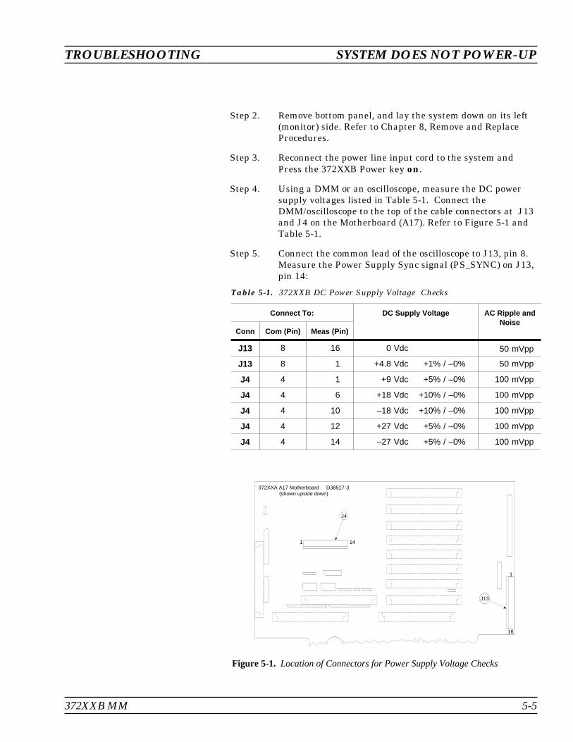
Step 2. Remove bottom panel, and lay the system down on its left(monitor) side. Refer to Chapter 8, Remove and ReplaceProcedures.
Step 3. Reconnect the power line input cord to the system andPress the 372XXB Power key on.
Step 4. Using a DMM or an oscilloscope, measure the DC powersupply voltages listed in Table 5-1. Connect theDMM/oscilloscope to the top of the cable connectors at J13and J4 on the Motherboard (A17). Refer to Figure 5-1 andTable 5-1.
Step 5. Connect the common lead of the oscilloscope to J13, pin 8.Measure the Power Supply Sync signal (PS_SYNC) on J13,pin 14:
TROUBLESHOOTING SYSTEM DOES NOT POWER-UP
372XXB MM 5-5
Connect To: DC Supply Voltage AC Ripple andNoise
Conn Com (Pin) Meas (Pin)
J13 8 16 0 Vdc 50 mVpp
J13 8 1 +4.8 Vdc +1% / –0% 50 mVpp
J4 4 1 +9 Vdc +5% / –0% 100 mVpp
J4 4 6 +18 Vdc +10% / –0% 100 mVpp
J4 4 10 –18 Vdc +10% / –0% 100 mVpp
J4 4 12 +27 Vdc +5% / –0% 100 mVpp
J4 4 14 –27 Vdc +5% / –0% 100 mVpp
Table 5-1. 372XXB DC Power Supply Voltage Checks
J13
J4
1
1
14
16
372XXA A17 Motherboard D38517-3(shown upside down)
Figure 5-1. Location of Connectors for Power Supply Voltage Checks

Specification: 2-4 vpp Sine Wave at 109.89 KHz
NOTEThe power supply module will power-up without thePS_SYNC signal being present. However, the lack ofthis signal will introduce signal purity problemswhen the system is performing measurements.
Power Supply ModuleCheck
If any of the DC voltage tests fail, verify that the power supply module isoperating properly with minimal impact from the system as described inthe procedures below.
NOTEIf a power supply voltage is low, it may be due to excessivecurrent draw from the system and not a fault in the powersupply.
Steps 1 through 4 verify the operation of the + 9, ±18, and ±27 Vdcsupplies:
Step 1. Press the 372XXB Power key off, and and disconnect thepower input cord.
Step 2. Disconnect the power supply module from the A17 Mother-board at J4.
Step 3. Reconnect the power line input cord to the system andpress the 372XXB Power key on.
Step 4. Using a DMM and/or an oscilloscope, measure the powersupply voltages at the power supply connector pins thatcorrespond to the Motherboard pins for the + 9, ±18, and±27 Vdc supplies. Refer to Table 5-1 and Figure 5-1 (previ-ous page).
Steps 5 through 8 check the +5 volt supply. This power supply re-quires at least a 10% load to turn on. Therefore, at least one of the dig-ital PCBs A9, A13, or A14 (which use the 5 volt supply) must be in-stalled in the system during this procedure.
Step 5. Press the 372XXB Power key off, and reconnect the powersupply module to the Motherboard at J4.
Step 6. Unplug digital PCB’s A13 and A14.
Step 7. Press the 372XXB Power key on.
Step 8. Using a DMM and/or an oscilloscope, measure the +5 voltpower supply at connector J13 on the Motherboard. Referto Figure 5-1 and Table 5-1, (page 505).
SYSTEM DOES NOT POWER-UP TROUBLESHOOTING
5-6 372XXB MM

Step 9. Press the 372XXB Power key off, and and reinstall the A13and A14 PCB’s removed in Step 6.
If any of the DC voltage tests fail in steps 1 through 8 above, replacethe power supply module.
If any of the DC voltage tests fail with the power supply module con-nected to the 372XXB Motherboard — but pass with it disconnected —then the most probable cause of the failure is that one of the 372XXBassemblies is demanding an excessive amount of current. To locate thefailed assembly:
1. Press the 372XXB Power key off, and unplug a single assembly.
2. Press the 372XXB Power key on, and note if the failed power sup-ply functions normally.
3. Repeat Steps 1 and 2 until an assembly is found that clears thepower supply failure. The removed assembly is suspect andshould be replaced.
5-5 SYSTEM DOES NOTBOOT-UP
If the 372XXB does not boot-up when it is powered-up, perform thechecks described below.
Boot-up ProcessSequence
The boot-up process is controlled by the firmware located on the A9PCB assembly (processor PROM) The boot-up activities include:
� Testing and initializing the A9 Main Processor PCB
� Testing communication between the A9 PCB and the digital PCBassemblies (A13, A14, A15, A16). The following messages will bedisplayed at this juncture:
� Initializing front panel knob (A14/A20)....
� Initializing GPIB (A13/A18)....
� Initializing external keyboard (A13)....
� Initializing external trigger (A13/A5)....
� Initializing front panel (A14/A20)....
� Loading of system software from disk into memory
� Starting operation of the system software.
� System is booting—message is displayed.
At this point, the system software continues the boot-up process byperforming the following activities:
� Issues command to A15 PCB to change display from TEXT modeto GRAPHIC mode and display ANRITSU logo.
TROUBLESHOOTING SYSTEM DOES NOT BOOT-UP
372XXB MM 5-7
� Performs basic communication tests between the digital system(A13, etc.) and the analog subsystem (A1-A8, A21A1, A21A2);this is part of a minimal self test.
� Conducts an IF Calibration
� Resets and loads the front panel state that was in effect prior tothe last power down
� Starts the measurement process
NOTEThe system software fully controls the 372XXB VNA sys-tem after boot-up (with operator intervention and guid-ance). The system software is only loaded once upon initialpower up.
TroubleshootingBoot-up Problems
To start the troubleshooting of boot-up related problems, perform thefollowing preliminary checks:
1. Note any error messages displayed on the CRT display during theboot-up process.
2. Observe the front panel and the display during the boot-up pro-cess for information as to which part of the process failed or didnot execute.
3. Verify that the system power supplies are working properly asper paragraph 5-4, above. Note particularly the operation ofpower supplies immediately after power-up.
4. Try to boot the instrument from the floppy disk and repeat steps1 and 2 above.
Upon completion of the preliminary checks (above), perform the fol-lowing procedures, as appropriate.
Hard Disk Problem 1 If a hard disk problem is indicated during bootup from a floppy disk, butthe system can bootup correctly from the hard disk:
Step 1. Boot up from the hard disk, then format the Hard Disk us-ing the procedure below.
CAUTIONFormatting the hard disk will erase all files on thehard disk. Before starting the disk formatting pro-cess, copy any files you wish to save to a floppy disk.
Step 2. Press the Utility Menu key (System State key group) to dis-
SYSTEM DOES NOT BOOT-UP TROUBLESHOOTING
5-8 372XXB MM

play the UTILITY FUNCTIONS OPTIONS menu. Frommenu, select GENERAL DISK UTILITIES (see below).
Step 3. If FLOPPY DISK UTILITIES menu appears, selectHARD DISK UTILITIES.
Step 4. From HARD DISK UTILITIES menu, select FORMATHARD DISK.
Step 5. After formatting is complete, reload System Software fromthe master floppy diskettes. Retry boot-up. If fail, contactANRITSU Customer Service Center.
Hard Disk Problem 2 If system does not bootup from hard disk and floppy disk:
Step 1. When the five initializing messages are displayed afterpower on, press any key within 2 seconds.
Step 2. Follow the instruction on the display to format the harddrive. After formatting is complete, reinstall system soft-ware from the master floppy diskettes. Retry boot-up.
Step 3. If fails, replace the A16 Hard Disk PCB; reinstall systemsoftware from the master floppy diskettes.
Step 4. Retry boot-up. If fail, contact ANRITSU Customer ServiceCenter.
Floppy Disk Problems If a floppy disk problem is indicated during bootup from floppy disk butthe system is able to bootup from the hard disk:
Step 1. Ensure the floppy disk media is in good condition
Step 2. Verify disk drive connection at Motherboard connector J2.
Step 3. Retry boot-up. If fail, replace the A13 - I/O#1 PCB.
Step 4. Retry boot-up. If fail, replace the Floppy Disk Drive.
TROUBLESHOOTING SYSTEM DOES NOT BOOT-UP
372XXB MM 5-9
SELECT UTILITYFUNCTION OPTIONS
GPIB ADDRESSES
DISPLAYINSTRUMENTSTATE PARAMS
GENERALDISK UTILITIES
CALIBRATIONCOMPONENTUTILITIES
l
l
FLOPPY DISKUTILITIES
DISPLAYDIRECTORY
DELETE FILES
COPY FILESTO HARD DISK
FORMATFLOPPY DISK
HARD DISKUTILITIES
HARD DISKUTILITIES
DISPLAYDIRECTORY
DELETE FILES
COPY FILESTO HARD DISK
FORMATHARD DISK
FLOPPY DISKUTILITIES

Screen DisplayProblems
If the 372XXB system appears to have no screen display, perform thepreliminary check below and then perform checks 1 - 3, as appropriate:
Preliminary Check - Press the 372XXB Power key off and then on sev-eral times. Each time power is reapplied, pause and wait for the372XXB software system to boot-up. During boot-up, observe the topleft hand portion of the CRT display.
NOTE� An alternative method to reset and re-boot the software system
is to press the red button on the A9 Main Processor PCB. Ob-serve the messages displayed on the screen during the boot-upprocess. Verify that the following messages are present :
� Initializing front panel knob (A14/A20)....
� Initializing GPIB (A13/A18)....
� Initializing external keyboard (A13)....
� Initializing external trigger (A13/A5)....
Check 1: If during boot-up the 372XXB does not attempt to display any mes-sages at all, proceed as follows:
Step 1. Replace the A15 Graphics Processor PCB.
Step 2. Retry boot-up. If fail, replace the Internal VGA Monitor.
Step 3. Retry boot-up. If fail, replace the A9, Main Processor PCB.
Step 4. Retry boot-up. If fail, contact ANRITSU Customer ServiceCenter.
Check 2: If the system halts before it completes all five digital sections, processas follows:
Step 1. Replace the PCB indicated on the last displayed message.Example: If the system halt at the “Initializing front panelknob (A14/A20)....,” replace the A14 and A20 PCBs.
Step 2. Retry to boot the system. If it still fails, contact ANRITSUCustomer Service.
5-6 SYSTEM PRODUCESERROR CODE
If the 372XXB detects a problem during normal operation, an error mes-sage consisting of an error code followed by a brief error message will bedisplayed on the screen. The error code will also be written to the servicelog along with some of the operating data gathered from the system atthe time of failure.
System error codes in the range 0100 - 3999 identify the suspectedfailed subassembly in the two most-significant digits of the error code.For example: error codes 0200 - 0299 are related to the A2, LO2 PCB
SYSTEM PRODUCES ERROR CODE TROUBLESHOOTING
5-10 372XXB MM

assembly. This error code assignment scheme allows for quick identifi-cation of suspect assemblies.
NOTERefer to Appendix B, Error Codes/Messages, for a list ofthe error codes/messages for 372XXB VNA systems.
There are cases when a fault on one assembly will cause a different as-sembly to be identified as faulty (per the error code designated). Thishappens when a failure occurs on an assembly that provides a stimu-lus or a calibration signal to other assemblies in the system. Example:the A7 LO3 PCB provides the IF Calibration signal to the A3, A4, andA6 PCB’s. If the IF Cal signal is faulty, error codes will be reported forthe A3, A4, A6, and A7 PCB’s.
NOTEAn aide to troubleshooting system failures using errorcodes is a good understanding of system and subassemblyoperation. Refer to the descriptions of system and subas-sembly operation and block diagrams located in Chapter 7,System Description.
Self Test Error Codes Error codes 0100 - 3999, with few exceptions, are produced as a resultof a failure when the system self test is run. These error codes will notbe displayed on the CRT screen. Only the overall result of the self test(PASS/FAIL) will be displayed at the conclusion of the self test. How-ever, any error codes due to the self test will be written to the servicelog as the self test is executed.
NOTEThe exceptions are error codes with 00 in the twoleast-significant digits, for example: 0500 A/D CONVER-SION FAIL. These errors are produced at run time if aproblem is encountered when the system is actively mak-ing measurements.
Phase Lock ErrorCodes (6000 Series)
The Phase Lock error codes (6000 - 6999) will have an alphabeticalsuffix (code) following the message. For example: 6079 PHS LCK FAILABCDG. This code consists of one or more letters from A - G that rep-resent the sub assembly that was not locked and/or the nature of thefailure. The phase lock failure mode suffixes are listed in Table 5-2.
Note that most phase lock error codes will normally consist of a letteridentifying the unlocked assembly and the D and/or DE letters thatindicate the Source Module is also unlocked. This is normal since allcomponents in the phase lock loop must be correctly locked in order forthe Source Module to achieve lock. Refer to Figure 5-2 for a flowchartthat troubleshoots the >40 GHz models (37297B).
TROUBLESHOOTING SYSTEM PRODUCES ERROR CODE
372XXB MM 5-11

Example 1: Any of the following error messages indicate that theLO1 PCB assembly was not able to lock:
6002 PHS LCK FAIL B
6010 PHS LCK FAIL BD
6026 PHS LCK FAIL BDE
Also note that if the 10 MHz Reference fails, depending on the failure,the system will not be able to lock any of the phase lock loop compo-nents: A1, A2, A7, A8, or Source Module.
Example 2: Either of the following error messages indicate a 10MHz Reference problem:
6001 PHS LCK A
6015 PHS LCK ABCDG
Service Log SnapShot Data
Error codes will be written to the service log along with some data repre-senting a “Snap Shot” of system conditions at the time of failure. Usually,the data included in the snap shot helps to provide faster diagnosis of theerror condition. The common snap shot data items that will be usefulinassembly level troubleshooting and fault diagnosis efforts are listed inTable 5-3.
NOTESome of the data included in the snap shot is useful onlyfor factory troubleshooting activities.
SYSTEM PRODUCES ERROR CODE TROUBLESHOOTING
5-12 372XXB MM
FailureSuffix
Failed Assembly/Failure Mode
FailureSuffix
Failed Assembly/Failure Mode
A 10 MHz not present E IF lock signal level too low
B L01 unlocked F Ext synthesizer unlocked
C L02 unlocked G L03 unlocked
D Source unlocked none Unknown
Table 5-2. Phase Lock Error Message Failure Suffixes

TROUBLESHOOTING SYSTEM PRODUCES ERROR CODE
372XXB MM 5-13
Item Description
SWP Sweep direction:F = forward (S11, S21), R = reverse (S22, S12)
PWR System source power setting
SYS System frequency setting
A The calibration results for the Test A Channel PCB (A3): This is aseries of 16 values divided into groups of four. Each group shouldhave values that are approximately 1
4 that of those in the previousgroup.
The first group data values should be approximately: 1.00 0.000.00 1.00. The values of the next group should be 1
4 that of thosevalues i.e., 0.25 0.00 0.00 0.25. The same applies for the valuesin the remaining two groups.
B The calibration results for the Test B Channel PCB (A6). See de-scription for “A” above.
R The calibration results for the Reference A (or B) Channel PCB(A4). See description for “A” above.
<OVL> Indicates the value was too far out of range to be measurable.
PHSLCK Source Locking: L=Source Lock Mode, T=Tracking Mode, S=Set OnMode
Table 5-3. Service Log Snap Shot Data Items (1 of 2)

DE LOCK FAILURE TROUBLESHOOTING
5-14 372XXB MM
Fails bothForward and
Reverse?
Lock Failure DECode 6XXX)(Error
Fails below38 GHz?
Fails above38 GHz?
Fails above38 GHz?
Normal power atPort 1?
Normal power atPort 1?
Normal power atPort 1?
OK 40MHzto 272MHz?
Power Amp orLO1 Failure
Buffer Amp, A4or A8 Failure
A8, Buffer AmpFailure
SDM, SW filter, XferSwitch, or source
PCB failure
Not logical. CallCustomer Service
Buffer Amp, PowerAmp, or A1 Failure
A8,YIG Osc, SW filter,or Source PCB Failure SPDT Switch, SW
Filter, A8 or SourcePCB Failure
Yes
Yes
Yes
Yes
Yes
Yes
Yes
No
No
No
No
No
No
NoNo
Yes
Yes
NOTE: Sampler/Buffer amplifiers are individually matched to
Power Amplifiers. If either fails, both should be replaced with
another matched set, part number ND53249.
Go to
1
See Sheet 2
Figure 5-2. Error Code DE Lock Failure Troubleshooting (37397A) (1 of 3)
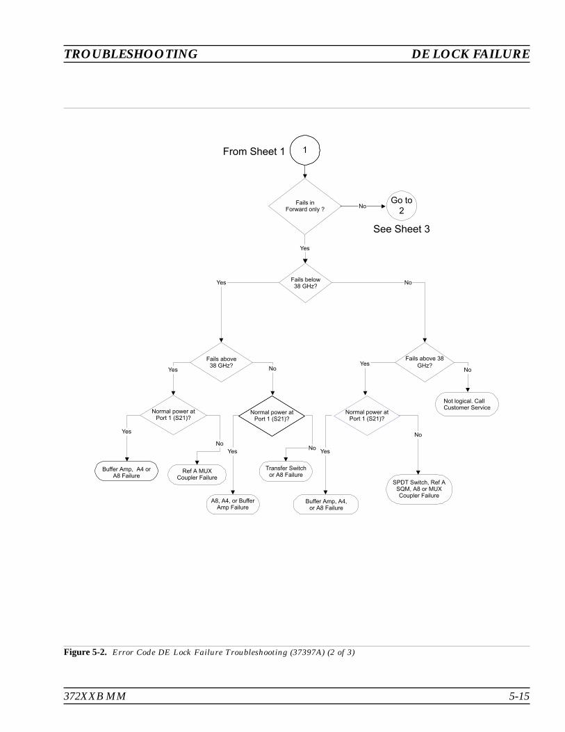
TROUBLESHOOTING DE LOCK FAILURE
372XXB MM 5-15
Fails inForward only ?
Fails below38 GHz?
Fails above38 GHz?
Fails above 38
GHz?
Normal power atPort 1 (S21)?
Normal power atPort 1 (S21)?
Normal power atPort 1 (S21)?
Buffer Amp, A4 orA8 Failure
A8, A4, or BufferAmp Failure
Transfer Switchor A8 Failure
Buffer Amp, A4,or A8 Failure
Ref A MUXCoupler Failure
SPDT Switch, Ref ASQM, A8 or MUXCoupler Failure
Yes
Yes
Yes
Yes
Yes
Yes
Yes
No
No
No No
No
NoNo
1
Go to
2
Not logical. CallCustomer Service
See Sheet 3
From Sheet 1
Figure 5-2. Error Code DE Lock Failure Troubleshooting (37397A) (2 of 3)

DE LOCK FAILURE TROUBLESHOOTING
5-16 372XXB MM
Reverse FailsOnly?
Yes
No
Fails below38 GHz?
Fails above38 GHz?
Fails above38 GHz?
Normal power atPort 2 (S12)?
Normal power atPort 2 (S12)?
Normal power atPort 2 (S12)?
Buffer Amp, A4or A8 Failure
A8, A4, or BufferAmp Failure
A8, transfer sw
failure
Buffer Amp, A8, orA4 Failure
Ref B MUX Failure
Ref B SQM, SPDTSwitch, A8, or MUX Failure
Yes
Yes Yes
Yes
Yes
Yes
No
No No
No
NoNo
2
Not logical. CallCustomer Service
Not logical. CallCustomer Service
From Sheet 1
Figure 5-2. Error Code DE Lock Failure Troubleshooting (37397A) (3 of 3)

5-7 SOURCE/TESTSET/RECEIVER
Because of the 372XXB phase-lock loop structure, it is not easy to distin-guish between failures that occur in the Source Module, the Test SetModule and the Receiver Module. In order to troubleshoot failures occur-ring in this group of modules, it is essential to be familiar with how eachmodule functions and how it interacts with the other modules. Refer toChapter 7, System description, for a functional description of each mod-ule.
For Model 37297B, refer to Figure 5-3 and Figure 5-4 (rear of section)for aid in troubleshooting Test and Source Lock signal paths. Referalso to Table 5-6 (rear of section) for a list of typical reference signalvalues, and to Tables 5-7 and -8 for Transfer and DPDT Switch Volt-ages.
Signal Source PhaseLock Loop Assemblies
The 372XXB assemblies that contain circuits that are part of the sig-nal source phase-lock loop (Source Lock function) are listed in Table5-4.
Failures occurring in the Source Module, Test Set Module and Re-ceiver Module will generally cause the system to produce “Phase LockFail” error codes. Included with the Phase Lock Fail error codes are al-phabetical suffixes that indicate the probable malfunctionedsub-assembly.
TROUBLESHOOTING SOURCE/TEST SET/RECEIVER
372XXB MM 5-17
Assemblies Location
A21A1 Source YIG/Bias PCB Source Module
A21A2 Source Control Source Module
YIG Oscillator Source Module
Switched Filter Source Module
Down Converter Source Module
Switched Doubler Module SDM* Test Set Module
Transfer Switch Test Set Module
Buffer Amplifier Receiver Module
A1 LO1 PCB Receiver Module
A2 LO2 PCB Receiver Module
A4 Reference IF PCB IF Section
A8 Source Lock/Signal Separation Control PCB Analog Subsystem
A9 Main Processor PCB Digital Subsystem
* Model 37269B only
Table 5-4. Phase Lock Loop Assemblies (2 of 2)

Example: 6008 PHS LCK FAIL D
The letter “D” in the error code above indicates that the failure is pos-sibly in the Source Module. (Refer to Table 5-3.)
Signal Source/TestSet Module Error
Codes
Failures occurring in the Signal Source Module and Test Set Module willalso produce the error codes listed in Table 5-5.
NOTEThe 372XXB has extensive built-in troubleshooting toolsthat are useful for troubleshooting the failures listed inTable 5-5. These and other troubleshooting tools are ac-cessed from the Option Menu key, which is part of the en-hancement keygroup. (From the select OPTIONS menuselect DIAGNOSTICS, then select TROUBLE-SHOOTING). Refer to Appendix A.
Troubleshooting tools that are available from the TROUBLE-SHOOTING menu that are useful for locating faults occurring in theSource Module, Test Set Module and Receiver Module are:
NOTEThe troubleshooting tools listed below are used to test the372XXB to factory set limits when the ANRITSU 372XXBTest Software (2300-178) is run.
When run from the TROUBLESHOOTING menu, not alltests will display limit lines (as is the case when the372XXB Test Software 2300-178 is used).
NON-RATIO PARAMETERSThis function displays the output of each of the individual test setchannels. It is especially useful for verifying the performance of theBuffer Amplifier and Power Amplifier.
SOURCE/TEST SET/RECEIVER TROUBLESHOOTING
5-18 372XXB MM
Error Codes Possible Failed Assemblies
5110 RF PWR UNLEVELED All components in Source Moduleand Test Set Module
5210 REF A CHAN RF OVERLOAD Transfer Switch
5220 REF B CHAN RF OVERLOAD Transfer Switch
5230 TA CHAN RF OVERLOAD Transfer Switch or A21A2 PCB
5240 TB CHAN RF OVERLOAD Transfer Switch or A21A2 PCB
Table 5-5. Signal Source/Test Set Module Error Codes

NOTEA through-line cable connecting Port 1 and Port 2 is re-quired for this check.
By examining these displays in conjunction with other failure symp-toms, the failed assembly can be located.
Example: Suppose the Non-Ratio Parameter screen display showspower holes above 270 MHz on all traces and in both sweep directions.A possible cause for this condition is a failure of the Power Amplifierassembly at certain frequencies. (Refer to Analog Subsystem Block Di-agram in Figure 7-2 on page 7-6).
LO1This function allows user to verify whether the A1 LO1 PCB is operat-ing properly.
LO2This function allows the user to verify whether the A2 LO2 PCB is op-erating properly.
SOURCEThis function allows the user to verify whether the Source Module isoperating properly.
Isolation Procedures The procedures in the following paragraphs will help you isolate the faultto the major assembly.
Check #1 Proceed as follows:
Step 1. Press Option Menu key and select the DIAGNOSTICS menuoption.
Step 2. Select the READ SERVICE LOG menu option to display theerror entry associated with the system failure. Observe thesnap shot data included as part of the error entry and note
TROUBLESHOOTING SOURCE/TEST SET/RECEIVER
372XXB MM 5-19
OPTIONS
TRIGGERS
REAR PANELOUTPUT
DIAGNOSTICS
MULTIPLE SOURCECONTROL
DIAGNOSTICS
START SELF TEST
READ SERVICE LOG
INSTALLED OPTIONS
PERIPHERAL TESTS
TROUBLESHOOTING(FOR SERVICEONLY)
HW CALIBRATIONS(FOR SERVICEONLY)

the sweep direction indication for each error code. (Refer toTable 5-3.)
Step 3. Determine whether the failure occurs during forward mea-surements (S11, S21) and/or reverse measurements (S22,S12):
If the problem occurs in both directions at all frequen-cies, the fault could be in the Receiver Module, SignalSource Module, or Test Set Module.
If the problem occurs in both directions at only certainfrequencies, the fault could be in the Signal Source Mod-ule.
If the problem occurs in only one direction, the faultcould be in the TEST SET MODULE.
Step 4. Run the 37XXX Test Software (2300-178) program to verifyoperation of the Buffer Amplifier, A1 LO1 PCB, A2 LO2PCB, and Source control PCB.
Use the information obtained in steps 1 – 4 above to determinewhether the failure occurs in the Source Module, Test Module or Re-ceiver Module. Replace the suspected failed assembly, and performany required adjustment(s). Then retest. If the 372XXB still fails, con-tact ANRITSU Customer Service Center for further assistance.
NOTETo obtain technical service support from your nearestANRITSU Customer Service Center, refer to Paragraph1-8, Service Support Information.
Check #2 If you have determined that the failure occurs in both sweep direc-tions, only at certain frequencies, and that Error Code 5110 is re-corded in the Service Log, use the following procedures to determinewhich assembly may have failed:
Step 1. Set the 372XXB Start and Stop frequencies for the follow-ing bands:
SOURCE/TEST SET/RECEIVER TROUBLESHOOTING
5-20 372XXB MM
Band Start Stop
1 22.5*/40 MHz 2.0 GHz
2 2.0 GHz Upper band-edgefrequency formodel. (20 GHzfor 37269B)

Step 2. If the problem occurs in Band 1, replace the Down Con-verter assembly and repeat test.
If it fails, contact ANRITSU Customer Service Center.
Step 3. If the problem only occurs in Band 3, replace the SwitchedDoubler Module assembly and repeat test.
If it fails, replace Switched filter and repeat test.
If it fails, contact ANRITSU Customer Service Center.
Step 4. If the problem only occurs in Band 2, replace Switched Fil-ter assembly and repeat test.
If it fails, contact ANRITSU Customer Service Center.
NOTEAfter replacing a component, perform a FrequencyCalibration and a RF power/ALC Calibration. Referto Chapter 6, Adjustments.
Check #3 If you have determined that failure occurs in both sweep directions, atall frequencies and Error Code 5110 is recorded in the Service Log, thefailed component could be any of the following assemblies:
1. Transfer Switch
2. Switched Doubler Module
3. YIG Oscillator
4. A21A1 YIG Bias PCB
5. A21A2 Source Control PCB
Replace the components listed above in sequence. After each replace-ment recalibrate unit (see note above) and retest. If 372XXB still fails,contact your nearest ANRITSU Customer Service Center.
5-8 PERIPHERALS/INTERFACE TEST
The following paragraphs contain procedures to be used for troubleshoot-ing 372XXB peripheral or interface test failures. Select the paragraphsubheading that corresponds to the test that failed.
CRT Display TestFailures:
If the CRT Display Test failed, troubleshoot as follows:
Step 1. Replace the CRT Monitor Assembly.
TROUBLESHOOTING PERIPHERALS/ INTERFACE TEST
372XXB MM 5-21

Step 2. Perform the CRT Monitor Test again; if fail, replace theA15, Graphics Processor PCB.
Step 3. Perform the CRT Monitor Test again; if fail, contactANRITSU Customer Service Center.
Front Panel TestFailures:
If the Front Panel Test failed, troubleshoot as follows:
Step 1. Replace the Front Panel Assembly.
Step 2. Perform the Front Panel Test again; if fail, replace the A14,I/O#1 PCB.
Step 3. Perform the Front Panel Test again; if fail, contactANRITSU Customer Service Center.
External KeyboardInterface Test
Failures:
If the External Keyboard Interface Test failed, troubleshoot as follows:
Step 1. Replace the A18, Rear Panel PCB.
Step 2. Perform the External Keyboard Interface Test again; if fail,replace the A13, I/O#1 PCB.
Step 3. Perform the External Keyboard Interface Test again; if fail,contact ANRITSU Customer Service Center.
Printer Interface TestFailures:
If the Printer Interface Test failed, troubleshoot as follows:
Step 1. Replace the A18, Rear Panel PCB.
Step 2. Perform the Printer Interface Test again; if fail, replace theA13, I/O#1 PCB.
Step 3. Perform the Printer Interface Test again; if fail, contactANRITSU Customer Service Center.
GPIB Interface TestFailures:
If the GPIB Interface Test failed, troubleshoot as follows:
Step 1. Replace the A18, Rear Panel PCB.
Step 2. Perform the GPIB Interface Test again; if fail, replace theA13, I/O#1 PCB.
Step 3. Perform the GPIB Interface Test again; if fail, contactANRITSU Customer Service Center.
5-9 MEASUREMENTS INQUESTION
If the 372XXB measurement quality is suspect, the following paragraphsprovide guidelines and hints for determining possible measurement qual-ity problems.
MEASUREMENTS IN QUESTION TROUBLESHOOTING
5-22 372XXB MM

The quality of 372XXB VNA measurements is determined by the fol-lowing test conditions and variables:
� Condition of the 372XXB.
� Quality and condition of the interface connections and connec-tors.
� Quality and condition of the calibration components,through-lines, adapters and fixtures.
� Surrounding environmental conditions at the time of the mea-surement.
� Selection and performance of the calibration for the DUT beingmeasured.
MeasurementConditions Check List
When determining possible measurement problems, check the follow-ing items:
1. Check the DUT and the calibration conditions:
� Ensure the Calibration Components Coefficients data hasbeen installed into the system from the Calibration Kit in use.
� Ensure the proper calibration was done for the device beingmeasured:
� For high insertion loss device measurements the calibra-tion should include isolation, high number of averages,and lower IF Bandwidth settings during the calibration.
� For high return loss device measurements the calibra-tion should also include a sliding load calibration.
� Check DUT mating connector(s) condition and pin depth.
� Measure an alternate known good DUT, if possible.
� Check if the environment is stable enough for the accuracy re-quired for the DUT measurement.
� The system should not be subjected to variations in tem-perature.
� The system should not be placed in direct sun light ornext to a changing cooling source, such as a fan or airconditioning unit.
2. Check the calibration using known good components from the cal-ibration kit. If measurements of these devices do not produce goodresults:
� Check through-cable stability including condition and pindepth. Replace with a known good cable, if necessary.
� Check condition and pin depth of calibration kit components.Replace with known good components, if necessary.
TROUBLESHOOTING MEASUREMENTS IN QUESTION
372XXB MM 5-23

� Check condition and pin depth of test port connectors. Replacewith known good ones if necessary.
NOTEThe procedures for performing pin depth measure-ments for the connectors used on ANRITSU productsare contained in Appendix C, Connector Mainte-nance Check Procedures.
3. Check the system performance as follows:
� Perform the Signal Path Tests that are part of the OperationalTests. Refer to Chapter 3, Operational Tests.
� Check Match, Directivity, and Dynamic Range as described inChapter 4, Performance Verification.
� Complete the remaining checks described in Chapter 4 (Per-formance Verification).
MEASUREMENTS IN QUESTION TROUBLESHOOTING
5-24 372XXB MM

TROUBLESHOOTING MEASUREMENTS IN QUESTION
372XXB MM 5-25
Frequency SQM In SDM Out MUX J4 MUX J1 Buffer Amp In
20 GHz NA +18 +6 NA -26
37 GHz NA +20 +4 NA -28
40 GHz +19 NA NA +14 -28
50 GHz +18 NA NA +14 -23
65 GHz +16 NA NA +10 -26
Table 5-6. Typical Reference Signal Values in dBm
Wire Color Below 38 GHz Above 38 GHz
S21 S12 S21 S12
Brown +2.0 -3.3 +2.0 +2.0
Black -6.7 +1.6 +1.6 +1.6
White +1.6 -6.8 +1.6 +1.6
Grey -3.3 +2.0 +2.0 +2.0
Table 5-7. Typical Transfer Switch Voltages (CW, Single Channel Display)
Wire Color Forward Reverse
Brown +1.2 -3.7
Grey -3.7 +1.2
Figure 5-8. Typical SPDT Switch Voltages (CW, Single Channel Display)
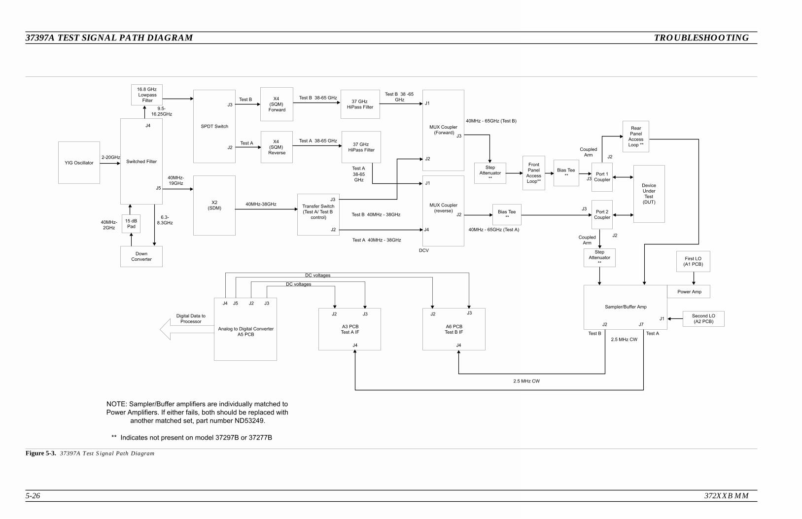
5-26 372XXB MM
37397A TEST SIGNAL PATH DIAGRAM TROUBLESHOOTING
YIG Oscillator
X4
(SQM)
Reverse
Switched Filter
Down
Converter
Analog to Digital Converter
A5 PCB
Sampler/Buffer Amp
X2
(SDM)
X4
(SQM)
Forward
MUX Coupler
(reverse)Transfer Switch
(Test A/ Test B
control)
37 GHz
HiPass Filter
37 GHz
HiPass Filter
Step
Attenuator
**
Bias Tee
**
MUX Coupler
(Forward)
A6 PCB
Test B IF
SPDT SwitchJ4
J5
Test B
Test A 38-65 GHz
Test B 38-65 GHz
Test A
A3 PCB
Test A IF
Power Amp
Second LO
(A2 PCB)
First LO
(A1 PCB)
Test B 40MHz - 38GHz
Test A 40MHz - 38GHz
Front
Panel
Access
Loop**
40MHz - 65GHz (Test B)
40MHz - 65GHz (Test A)
J3
2.5 MHz CW
J2J2
Test B 38 -65
GHz
Test A
38-65
GHz
J2
J1
J4J2
J3
J2
DCV
J1J3
J2
40MHz-
2GHz
6.3-
8.3GHz
2-20GHz
40MHz-
19GHz
9.5-
16.25GHz
40MHz-38GHz
J3
Port 2
Coupler
Device
Under
Test
(DUT)
Port 1
Coupler
Bias Tee
**
Rear
Panel
Access
Loop **
J4
J4 J5 J2 J3
J4
J3
J2 J7
DC voltages
DC voltages
2.5 MHz CW
Step
Attenuator
**
Coupled
Arm
Coupled
Arm
Digital Data to
Processor
J3
J2
J3
J2
J1
Test B Test A
16.8 GHz
Lowpass
Filter
15 dB
Pad
NOTE: Sampler/Buffer amplifiers are individually matched to
Power Amplifiers. If either fails, both should be replaced with
another matched set, part number ND53249.
** Indicates not present on model 37297B or 37277B
Figure 5-3. 37397A Test Signal Path Diagram

372XXB MM 5-27/5-28
TROUBLESHOOTING 37397A SOURCE LOCK SIGNAL PATH DIAGRAM
YIG Oscillator
X4
(SQM)
Reverse
Switched Filter
Down
Converter
A21A2 PCB
Sampler/Buffer AmpX2
(SDM)
3 dB pad
X4
(SQM)
Forward
MUX Coupler
(reverse)
3 dB Pad
Transfer Switch
(Ref A/ Ref B
Control)
37 GHz
HiPass Filter
37 GHz
HiPass Filter
Shaped Pad
Shaped Pad
MUX Coupler
(forward)
A21A1 PCBA4 PCB
Reference IF Processor
SPDT SwitchJ4
J5
Ref A
Ref B 38-65 GHz
Ref A 38-65 GHz
Ref B
A8 PCB
Source Lock/ RF
Component Control
Power Amp
Second LO
(A2 PCB)
(25-272MHz)
First LO
(A1 PCB)
(357-536MHz)
Ref A 40MHz - 38GHz
Ref B 40MHz - 38GHz
Rear
Panel
Access
Loop **
40MHz-65GHz (Ref A)
40MHz -65GHz (Ref B)
ALC Control PCB
49808-3
Ref A
J7J8
Ref B
2.5 MHz CW
2.5 MHz CWJ4J2J1J1
J3
Ref A 38-65 GHz
Ref B
DC
voltage
38-65
GHz
DC voltage (6 MHz / Volt)
J4
J1
J4J4
J5
J5
DCV
DCV
J1J3
J2
YIG tuning currents
Digital and Analog Control
40MHz-
2GHz
6.3-
8.3GHz
2-20GHz
40MHz-
19GHz
9.5-
16.25GHz
40MHz-38GHz
SDM Control
Bias Voltages to YIG,Switched Filter
Down Converter, SAM
Control of SPDT
switch, transfer switch,
buffer amp, power
amp, ALC control
J5
J5 J3
J1
3 dB pad
3 dB pad
16.8 GHz
Lowpass
Filter
15 dB
Pad
NOTE: Sampler/Buffer amplifiers are individually matched to
Power Amplifiers. If either fails, both should be replaced with
another matched set, part number ND53249.
3 dB Pad
** Indicates not present on model 37297B or 37277B
3 dB pad
Figure 5-4. 37397A Source Lock Signal Path Diagram

Contents6-1 INTRODUCTION · · · · · · · · · · · · · · · · · · · · · · · · · 6-3
6-2 LO1 CALIBRATION· · · · · · · · · · · · · · · · · · · · · · · · 6-3Calibration Procedure · · · · · · · · · · · · · · · · · · · · · · · 6-3Post Calibration Actions· · · · · · · · · · · · · · · · · · · · · · 6-3
6-3 LO 2 CALIBRATION · · · · · · · · · · · · · · · · · · · · · · · 6-4Calibration Procedure · · · · · · · · · · · · · · · · · · · · · · · 6-4Post Calibration Actions· · · · · · · · · · · · · · · · · · · · · · 6-5
6-4 FREQUENCY CALIBRATION · · · · · · · · · · · · · · · · · · 6-5Calibration Procedure · · · · · · · · · · · · · · · · · · · · · · · 6-6Post Calibration Actions· · · · · · · · · · · · · · · · · · · · · · 6-7
6-5 RF POWER/ALC CALIBRATION· · · · · · · · · · · · · · · · · 6-8Calibration Procedure · · · · · · · · · · · · · · · · · · · · · · · 6-8Post Calibration Actions· · · · · · · · · · · · · · · · · · · · · · 6-9
Chapter 6Adjustments


Chapter 6Adjustments
6-1 INTRODUCTION This chapter contains five procedures that are used to restore the calibra-tion of the 372XXB signal source and the related source lock system as-semblies. Use these procedures after various signal source related assem-blies have been replaced due to troubleshooting or repair activities.
Refer to paragraph 6-7 and 6-8 for recalibrations, which are necessaryif certain subassemblies are replaced.
Please insure you have read and fully understand the servicing con-cepts for the 372XXB presented in Chapter 1 prior to continuing withthis chapter.
6-2 LO1 CALIBRATION This procedure uses the 372XXB internal diagnostics and calibrationmenus to adjust the A1 1st LO PCB assembly. Perform this calibationprocedure if:
� The A1 PCB is replaced.
� BBRAM chip on A9 Processor PCB is replaced and the SourceLock Threshold Calibration data was not previously saved ondisk (that is, data is not available for recall from a floppy disk).
CalibrationProcedure
Perform the following steps:
Equipment Required
None
NOTEAllow the 372XXB to warm-up at least 30 minutes prior toperforming calibration.
Procedure
Step 1. Press the Option Menu key (Enhancement key group) to dis-play the OPTIONS menu.
Step 2. Select DIAGNOSTICS from menu.Then select in se-quence: H/W CALIBRATIONS then LO1 CALIBRA-TION.
Step 3. Follow the directions displayed on the 372XXB CRT screen,until calibration is completed.
372XXB MM 6-3

Post CalibrationActions
After the calibration process is completed, perform the following ac-tions, as appropriate:
If calibration passes:
Save the calibration data to (hard) disk, as follows:
Step 1. Press the Option Menu key (Enhancement key group) to dis-play the OPTIONS menu.
Step 2. Select DIAGNOSTICS from menu.Then select in se-quence: H/W CALIBRATIONS |DISK OPERATIONS|SAVE TO HARD DISK|HW_CAL.LO1.
NOTEAlso save the calibration data to floppy diskfor archival purposes as a backup in case ofa hard disk failure. Label the disk with cali-bration type, date, and system model and se-rial numbers. Set the copy protect tab on thedisk. Properly safeguard the disk so that itwill be available for later use, as needed.
If calibration fails:
Step 3. Repeat the calibration. If it still fails, then proceed toChapter 5, Troubleshooting.
6-3 LO 2 CALIBRATION This procedure uses the 372XXB internal diagnostics and calibrationmenus to adjust the A2 1st LO PCB assembly. Perform this calibationprocedure if:
� The A2 PCB is replaced.
� BBRAM chip on A9 Processor PCB is replaced and the SourceLock Threshold Calibration data was not previously saved ondisk (that is, data is not available for recall from a floppy disk).
CalibrationProcedure
Perform the following steps:
Equipment Required
None
NOTEAllow the 372XXB to warm-up at least 30 minutes prior toperforming calibration.
LO 2 CALIBRATION ADJUSTMENTS
6-4 372XXB MM

Procedure
Step 1. Press the Option Menu key (Enhancement key group) to dis-play the OPTIONS menu.
Step 2. Select DIAGNOSTICS from menu.Then select in se-quence: H/W CALIBRATIONS then LO2 CALIBRA-TION.
Step 3. Follow the directions displayed on the 372XXB CRT screen,until calibration is completed.
Post CalibrationActions
After the calibration process is completed, perform the following ac-tions, as appropriate:
If calibration passes:
Save the calibration data to (hard) disk, as follows:
Step 1. Press the Option Menu key (Enhancement key group) to dis-play the OPTIONS menu.
Step 2. Select DIAGNOSTICS from menu.Then select in se-quence: H/W CALIBRATIONS |DISK OPERATIONS|SAVE TO HARD DISK|HW_CAL.LO2.
NOTEAlso save the calibration data to floppy diskfor archival purposes as a backup in case ofa hard disk failure. Label the disk with cali-bration type, date, and system model and se-rial numbers. Set the copy protect tab on thedisk. Properly safeguard the disk so that itwill be available for later use, as needed.
If calibration fails:
Repeat the calibration. If it still fails, then proceed to Chapter 5, Trou-bleshooting.
6-4 FREQUENCYCALIBRATION
This procedure uses the internal 372XXB diagnostics and calibrationmenus, in conjunction with a suitable frequency counter, to adjust thesignal source frequencies throughout the range of the 372XXB model be-ing calibrated. Perform this calibration procedure if:
� The Source FM/Lock Linearity test in Chapter 3, OperationalTest, fails.
� Other testing or troubleshooting reveals a possible problem withthe signal source frequency accuracy or phase lock loop.
� Any of the following assemblies are replaced:
ADJUSTMENTS FREQUENCY CALIBRATION
372XXB MM 6-5

� A21A1 Source YIG/Bias
� A21A2 Source Controller
� Down Converter
� YIG Oscillator
� Switched Filter
� Buffer Amplifier
� BBRAM chip on the A9 Processor PCB is replaced and theSource Calibration Data was not previously saved on disk (thusdata could not be recalled from disk).
CalibrationProcedure
Perform the following steps:
Equipment Required
Refer to Table 1-1, located on page 1-10, for further information aboutthe following equipment:
EIP Model 578B Frequency Counter, or equivalent.
RF/Microwave Cable
GPIB cable, ANRITSU 2100-2, or equivalent
NOTEAllow the 372XXB and Frequency Counter to warm-up atleast 30 minutes prior to performing calibration.
Procedure
Step 1. Set up test equipment as shown in Figure 6-1.
FREQUENCY CALIBRATION ADJUSTMENTS
6-6 372XXB MM
� � � � � �
� � � � � �
� � � � � �
�
� �
� � �
� � �
� � � � � � � � � � � � � � � � �
� � � � � � ! " � # $ � % � " � � �
& � � # � � � � ' � � � � � � � � ( � # ) * � + � � ' � � � � # � � � # � � � ,
- � # � � + � . � % � / �
Figure 6-1. Test Equipment Setup for Frequency Calibration

Step 2. Press the Option Menu key (Enhancement key group) to dis-play the OPTIONS menu.
Step 3. Select DIAGNOSTICS from menu; then select in se-quence: H/W CALIBRATION, and then SOURCEFREQUENCY CALIBRATION (below).
Step 4. Follow the directions displayed on the screen to set-up andconnect the frequency counter to the 372XXB. Refer also toFigure 6.1 (next page). Select START SOURCEFREQ CALIBRATION from menu (above).
Step 5. Follow the directions displayed on the 372XXB CRT screen,until calibration is completed.
Post CalibrationActions
After the calibration process is completed, perform the following ac-tions, as appropriate:
If calibration passes:
Save the calibration data to (hard) disk, as follows:
Step 1. Press the Option Menu key (Enhancement key group) to dis-play the OPTIONS menu.
Step 2. Select DIAGNOSTICS from menu.Then select in se-quence: H/W CALIBRATIONS |DISK OPERATIONS|SAVE TO HARD DISK |HW_CAL.FRE.
NOTEAlso save the calibration data to floppy diskfor archival purposes as a backup in case ofa hard disk failure. Label the disk with cali-bration type (FRE), date, and system modeland serial numbers. Set the copy protect tabon the disk. Properly safeguard the disk so
ADJUSTMENTS FREQUENCY CALIBRATION
372XXB MM 6-7
OPTIONS
TRIGGERS
REAR PANELOUTPUT
DIAGNOSTICS
MULTIPLE SOURCECONTROL
DIAGNOSTICS
START SELF TEST
READ SERVICE LOG
INSTALLED OPTIONS
PERIPHERAL TESTS
TROUBLESHOOTING(FOR SERVICEONLY)
H/W CALIBRATIONS(FOR SERVICEONLY)
HARDWARECALIBRATIONS(FOR SERVICE
ONLY)
LO1CALIBRATION
LO2CALIBRATION
SOURCE FREQUENCYCALIBRATION
SOURCE ALCCALIBRATION
DISK OPERATIONS
PREVIOUS MENU
HARDWARECALIBRATIONS(FOR SERVICE
ONLY)
START ALCFREQ CALIBRATION
PREVIOUS MENUSet-U

that it will be available for later use, asneeded.
Perform the Source FM/Lock Linearity test in Chapter 3, OperationalTests. If the test fails, proceed to Chapter 5, Troubleshooting.
If calibration fails:
� Verify the GPIB cable is connected to the Dedicated GPIB (bot-tom) connector on the 372XXB rear panel.
� Verify that the frequency counter is functioning correctly, the ca-ble is in good condition, and all connections are secure.
� Note which calibration step failed from the screen messages.
� Repeat the calibration. If it still fails, then proceed to Chapter 5,Troubleshooting.
6-5 RF POWER/ALCCALIBRATION
This procedure uses the 372XXB internal diagnostics and calibrationmenus, in conjunction with a suitable power meter, to adjust the out-put power level of the signal source throughout the range of the372XXB model being calibrated. Perform this calibration procedure if:
� The Source Power/ALC test in Chapter 3, Operating Test, fails.
� Other testing or troubleshooting reveals a possible problem withRF Power accuracy or the ALC loop.
� Any of the following assemblies are replaced:
� A21A1 Source YIG/Bias
� A21A2 Source Controller
� Down Converter
� YIG Oscillator
� Switched Filter
� Transfer Switch
� SDM (37269B)
� Coupler (37225B and above)
� Bridge (37217B and below)
� Buffer Amplifier
� BBRAM chip on the A9 Processor PCB is replaced and theSource Calibration Data was not previously saved on disk (thusdata could not be recalled from disk).
RF POWER/ALC CALIBRATION ADJUSTMENTS
6-8 372XXB MM

CalibrationProcedure
Perform the following steps:
Equipment Required
Refer to Chapter 1, Table 1-1, page 1-9, for further information aboutthe following equipment:
HP 437B Power Meter with HP 8487A Power Sensor
or:
ANRITSU ML24XXA with Version 2.02 or later, with ANRITSUPower Sensors MA2474A and SC6230 for 65 GHz units.
or:
Gigatronics 8541/8542 with 80304A Power Sensor
GPIB cable, WILTRON 2100-2, or equivalent
NOTEAllow the 372XXB and power meter to warm-up at least30 minutes prior to performing calibration.
65 GHz Power Sensor Setup Procedure
The Anritsu SC6230 Power Sensor has an internal frequency calibra-tion factors table. The ML24XX meter settings must be changed sothat the table will be used for frequencies above 50 GHz. To configurethe meter for the new calibration factors table, proceed as follows:
Step 1. Press the Sensor key then Cal Factor softkey.
Step 2. Press the More softkey.
Step 3. Press the Use Table sofkey. Cursor will start blinking.
Step 4. Press 1 then the Enter softkey.
Step 5. Press the System key to exit.
Procedure
Step 6. Press the Option Menu key (Enhancement key group) todisplay the OPTIONS menu.
Step 7. Select DIAGNOSTICS from menu; then select in se-
ADJUSTMENTS RF POWER/ALC CALIBRATION
372XXB MM 6-9

quence: H/W CALIBRATIONS, and then SOURCE ALCCALIBRATION (below).
Step 8. Follow the directions displayed on the screen to set-up andconnect the power meter to the 372XXB. Refer also to Fig-ure 6-2. Select START ALC CALIBRATION from menu.
Step 9. Follow the directions displayed on the 372XXB CRT screen,until calibration is completed.
Post CalibrationActions
After the calibration process is completed, perform the following ac-tions, as appropriate:
If calibration passes:
Save the calibration data to (hard) disk, as follows:
RF POWER/ALC CALIBRATION ADJUSTMENTS
6-10 372XXB MM
� � �
� � �
� �
� �
� � � � � � � � �
� � � � � � � � � � � �� � �
� � � ! " # � � � $ % � � � & ' � ( � � � $ % � � � ! � � � � ! # � � )
� � � � � � � * ' � � � � �% � ( � � � * � # � �
Figure 6-2. Test Equipment Setup for Power Calibration
OPTIONS
TRIGGERS
REAR PANELOUTPUT
DIAGNOSTICS
MULTIPLE SOURCECONTROL
DIAGNOSTICS
START SELF TEST
READ SERVICE LOG
INSTALLED OPTIONS
PERIPHERAL TESTS
TROUBLESHOOTING(FOR SERVICEONLY)
H/W CALIBRATIONS(FOR SERVICEONLY)
HARDWARECALIBRATIONS(FOR SERVICE
ONLY)
LO1CALIBRATION
LO2CALIBRATION
SOURCE FREQUENCY
CALIBRATION
SOURCE ALCCALIBRATION
DISK OPERATIONS
PREVIOUS MENU
HARDWARECALIBRATIONS(FOR SERVICE
ONLY)
START SOURCEFREQ CALIBRATION
PREVIOUS MENUSet-Up
Step 1. Press the Option Menu key (Enhancement key group) to dis-play the OPTIONS menu.
Step 2. Select DIAGNOSTICS from menu.Then select in se-quence: H/W CALIBRATIONS |DISK OPERATIONS|SAVE TO HARD DISK|HW_CAL.ALC.
NOTEAlso save the calibration data to floppy diskfor archival purposes as a backup in case ofa hard disk failure. Label the disk with cali-bration type (ALC), date, and system modeland serial numbers. Set the copy protect tabon the disk. Properly safeguard the disk sothat it will be available for later use, asneeded.
Perform the RF Power Generation and Control test in Chapter 3, Op-erational Tests. If the test fails, proceed to Chapter 5, Trouble-shooting.
If calibration fails:
� Verify the GPIB cable is connected to the Dedicated GPIB (bot-tom) connector on the 372XXB rear panel.
� Verify that the power meter and sensor are functioning correctly,the cables are in good condition, and all connections are secure.
� Verify the correct power sensor data exists in the power meter.
� Note the failed step in the calibration procedure from the screenmessages.
� Repeat calibration. If it still fails then proceed to Chapter 5,Troubleshooting.
6-6 SOURCE LOCKTHRESHOLD
This procedure is only for the 37297B. It uses the 372XXB internal di-agnostics and calibration menus to adjust the source lock threshold ofthe phase-lock loop. Perform this calibation procedure if:
� The A4 PCB is replaced.
� BBRAM chip on A9 Processor PCB is replaced and the SourceLock Threshold Calibration data was not previously saved ondisk (that is, data is not available for recall from a floppy disk).
CalibrationProcedure
Perform the following steps:
Equipment Required
Two broadband terminations or one 3670V50-2 cable.
ADJUSTMENTS SOURCE LOCK THRESHOLD
372XXB MM 6-11

NOTEAllow the 372XXB to warm-up at least 30 minutes prior toperforming calibration, and perform the ALC calibration(paragraph 6-3) before doing this calibration.
Procedure
Step 1. If recalibrating a 37397A , install broadband terminationsto both ports or install a throughline between ports.
Step 2. Press the Option Menu key (Enhancement key group) to dis-play the OPTIONS menu.
Step 3. Select DIAGNOSTICS from menu.Then select in se-quence: H/W CALIBRATIONS then SOURCE THRESH-OLD CALIBRATION.
Step 4. Follow the directions displayed on the 372XXB CRT screen,until calibration is completed.
Post CalibrationActions
After the calibration process is completed, perform the following ac-tions, as appropriate:
If calibration passes:
Save the calibration data to (hard) disk, as follows:
Step 1. Press the Option Menu key (Enhancement key group) to dis-play the OPTIONS menu.
Step 2. Select DIAGNOSTICS from menu.Then select in se-quence: H/W CALIBRATIONS |DISK OPERATIONS|SAVE TO HARD DISK|HW_CAL.SLT.
NOTEAlso save the calibration data to floppy diskfor archival purposes as a backup in case ofa hard disk failure. Label the disk with cali-bration type, date, and system model and se-rial numbers. Set the copy protect tab on thedisk. Properly safeguard the disk so that itwill be available for later use, as needed.
If calibration fails:
� Repeat the calibration. If it still fails, then proceed to Chapter 5,Troubleshooting.
6-7 A8 ADJUSTMENT This procedure is only for the 37297B. The adjustments are importantto the operation of the VNA above 56 GHz. Improperly adjusted A8
A8 ADJUSTMENT ADJUSTMENTS
6-12 372XXB MM

Potentiometers may cause lock failures. Perform these adjustments asfollows:
� The A8 PCB is replaced.
� 44733 Buffer Amp is replaced.
CalibrationProcedure
Perform the following steps:
Equipment Required
V Throughline (3670V50-2 with FF Adapter)
NOTEAllow the 372XXB to warm-up at least 30 minutes prior toperforming calibration, and perform the ALC calibration(paragraph 6-3) before doing this calibration.
Procedure
Step 1. Connect a V Throughline (3670V50-2 with FF Adapter) be-tween Ports 1 and 2.
Step 2. Set the 372XXB to sweep from 50 to 65 GHz.
Step 3. Set RF power to 0 dB (default value).
Step 4. Using Diagnostics menu, view Non-Ratio parameters.
Step 5. View Channel 1 (Ref A) only, and activate Autoscale.
Step 6. Adjust the “RA” potentiometer on top of A8 for the flattesttrace display. A small discontinuity at 56 GHz is normal.
Step 7. Perform Step 6 for each of the four Non-Ratio channels.
6-8 A21A2 ADJUSTMENT This procedure is only for the 37297B. This adjustment ensures thecorrect RF power level will be available to drive the source quadruplermodules (SQMs). Perform these adjustments as follows:
� D454244 is replaced.
� A21A2 PCB is replaced.
� C21620 YIG Oscillator is replaced.
NOTEFailure to perform this adjustment may result in intermit-tent operation.
CalibrationProcedure
Perform the following steps:
ADJUSTMENTS A21A2 ADJUSTMENT
372XXB MM 6-13

Refer to Table 1-1, located on page 1-9, for further information aboutthe following equipment:
HP 437B Power Meter with HP 8487A Power Sensor
or:
ANRITSU ML24XXA with Version 2.02 or later, with ANRITSUPower Sensor MA2474A
or:
Gigatronics 8541/8542 with 80304A Power Sensor
GPIB cable, WILTRON 2100-2, or equivalent
NOTEAllow the 372XXB and power meter to warm-up at least30 minutes prior to performing calibration.
Procedure
Step 1. With power off and the new part installed, disconnect theRF cable from J4 of the Switched Filter.
Step 2. Install Power Sensor (use a 6 or 10 dB pad for protection)to Switched Filter J4.
Step 3. Turn on the 372XXB and set it to 38 GHz, CW.
Step 4. Adjust A21A2R238 for maximum power, but not over +26dBm.
Step 5. Remove the pad and sensor and reconnect the RF cable toJ4.
Step 6. Perform the procedures in paragraph 6-4 and 6-5 (fre-quency and ALC calibrations).
A21A2 ADJUSTMENT ADJUSTMENTS
6-14 372XXB MM

Table of Contents7-1 INTRODUCTION · · · · · · · · · · · · · · · · · · · · · · · · · 7-3
7-2 SYSTEM OVERVIEW · · · · · · · · · · · · · · · · · · · · · · · 7-3
7-3 ANALOG SUBSYSTEM ASSEMBLIES · · · · · · · · · · · · · 7-7Signal Source Module · · · · · · · · · · · · · · · · · · · · · · · 7-7Test Set Module · · · · · · · · · · · · · · · · · · · · · · · · · · 7-8Receiver Module · · · · · · · · · · · · · · · · · · · · · · · · · 7-10A8, Source Lock/Signal Separation andControl PCB · · · · · · · · · · · · · · · · · · · · · · · · · · · 7-11IF Section · · · · · · · · · · · · · · · · · · · · · · · · · · · · · 7-11A7 PCB, LO3 · · · · · · · · · · · · · · · · · · · · · · · · · · · 7-11A5 A/D Converter PCB · · · · · · · · · · · · · · · · · · · · · · 7-12
7-4 DIGITAL SUBSYSTEM ASSEMBLIES· · · · · · · · · · · · · 7-15A9 Main Processor PCB Assembly· · · · · · · · · · · · · · · · 7-15A13 I/O Interface #1 PCB Assembly · · · · · · · · · · · · · · · 7-16A14 I/O Interface #2 PCB Assembly · · · · · · · · · · · · · · · 7-16A15 Graphics Processor PCB Assembly · · · · · · · · · · · · · 7-17A16 Hard Disk PCB Assembly · · · · · · · · · · · · · · · · · · 7-17Floppy Disk Drive Assembly · · · · · · · · · · · · · · · · · · 7-17A24 VME Bus Terminator PCB · · · · · · · · · · · · · · · · · 7-17
7-5 MAIN CHASSIS ASSEMBLIES · · · · · · · · · · · · · · · · · 7-17A17 System Motherboard Assembly · · · · · · · · · · · · · · · 7-17Front Panel Assembly · · · · · · · · · · · · · · · · · · · · · · 7-17Rear Panel Assembly · · · · · · · · · · · · · · · · · · · · · · · 7-18A18 Rear Panel Interface PCB· · · · · · · · · · · · · · · · · · 7-18Power Supply Module · · · · · · · · · · · · · · · · · · · · · · 7-18Internal VGA Monitor · · · · · · · · · · · · · · · · · · · · · · 7-20A7 PCB, 10 MHz Timebase · · · · · · · · · · · · · · · · · · · 7-13
Chapter 7System Description


Chapter 7System Description
7-1 INTRODUCTION This chapter provides a brief overview of the functional assembliesand major parts that comprise a typical Series 372XXB VNA system.It also briefly describes the operation of each major assembly.
7-2 SYSTEM OVERVIEW Series 372XXB Vector Network Analyzers are ratio measurement sys-tems used to measure complex vector signal characteristics (real/imagi-nary, magnitude/phase, etc) of devices and systems in the 22.5 MHz to 65GHz frequency range.
The 372XXB performs these measurements by sourcing a stimulussignal to the Device Under Test (DUT) that is connected to the frontpanel Port 1 and/or Port2 connectors. (See Figure 7-1 on page 7-5). Itsimultaneously measures the DUT response, which consists of re-flected and/or transmitted (attenuated, or amplified) signals at theconnectors of the DUT. The reflected and/or transmitted signal(s) anda sample of the stimulus signal, are down converted and then trans-formed into their real and imaginary vector components. The resul-tant vector components are measured and converted into digital infor-mation. This digital information is sent to the Main Processor PCBwhere the desired S-parameter data is normalized and then presentedto the user via the front panel color display. The display information isalso sent to the rear panel VGA Out connector for use with an externalVGA monitor.
The normalized measurement information is also sent to the rearpanel Printer Out connector for use with an external printer and/orplotter.
A front panel keypad, a rotary knob, and an IBM compatible keyboardinterface provide user interaction with 372XXB Main Processor PCB.
The system is equipped with internal hard disk and floppy disk drivesand battery backed internal memories for storage and retrieval of dataand front panel setup information.
The 372XXB implements an IEEE 488.2 interface. This GPIB inter-face allows an externally connected instrument controller to controlthe 372XXB system in the “Remote-Only” mode. All 372XXB measure-ment and input/output operations may be controlled remotely in thismode.
372XXB MM 7-3

An internal service log stores a record of system failures, data aboutthe failures, and other key system service information. The service logis implemented using internal battery-backed SRAM memory.
SYSTEM OVERVIEW SYSTEM DESCRIPTION
7-4 372XXB MM

372XXB MM 7-5
SYSTEM DESCRIPTION OVERALL BLOCK DIGRAM
A/D
S/H
S/H
ANALOGMUX
S/H
S/H
S/H
CTL
EXTERNALKEYBOARD
A/D BUS
QUIET BUS
VMEINTERFACE
TO ANALOG PCB'S(CTL & DATA)
S/HS
S
S
D
D
D
YIG
PORT 1
PORT 2
0-70dBS.A
SDM
LOCKDET
QUADSAMPLER/BUFFER IF / SYNC/ DET
* MODEL 37269A ONLY
FLTR / S/H / A/D
2X
F
LVLDET
LVLDETF
R
RALC
SWITCHEDFILTER
DOWNCONV
SIGNAL SOURCE
TEST SET MODULE
DOUBLER
YIG OSC2-20 GHz
µP
µP
µP68030
S
S
S
STB
RB
RA
TA
HARMGEN
L.O.#1
L.O.#2
L.O.#3
REF OSC
10 MHz
I/O CONTROLLOGIC
QUIET BUSINTERFACE
&CONTROL
A/D BUSINTERFACE
&CONTROL
EXTERNALKEYBOARDINTERFACE
I/O PCB'S
FRONTPANEL
INTERFACE
FLOPPYDISK DRIVECONTROL
REAR PANELINTERFACE
&CONTROL
FLOPPYDISK
DRIVE
HARDDISK
DRIVE
RAM
INTERFACECTL
GRAPHICSPROCESSOR
PCB
INTERNALVGA
MONITOR
EXT VGA MONITOR
R.P.LOGICCKTS
REARPANEL
PCB
GPIBINTERFACE
VME BUS
MAIN PROCESSOR PCB
BBRAM
FRONTPANEL
PCB
Figure 7-1. Overall Block Digram of 372XXB VNA System

7-6 372XXB MM
ANALOG SUBSYSTEM BLOCK DIAGRAM SYSTEM DESCRIPTION
P1
D/A
P2
D/A
80KHz
÷20 ÷M
÷10 ÷K
1MHz
D/A
207-403MHz1MHz RES
10 MHz
2 BITS
NCO10 MHz
QB*
QB*QB*
QB*
QB*
QB*
QB* QB*
QB*
9-10MHz1Hz RES
D/A
SOURCETRACK
(A8)
197-394M1Hz RES
÷2,4,8
25.0-272.5MHz1Hz RES
25.0-272.5MHz1HZ RES
÷20
÷121
400K
10 MHz ÷25
48.4MHz
2.42MHz
CAL
80KHz
D/A
SINROM
÷125
10 MHz
EXT 10M OUT
EXT 10M IN
EXT
INT
10 MHz
A1
1ST LOA2
2ND LO
A7
3RD LO
H
10 MHz
-6MHz/V
A21A2
SOURCE
CONTROL
H
IRM
RA
RFF
RB
SOURCE LOCK(A4)
SOURCELOCK (A8)
LVLDET
LVLTHRDAC
10 MHz
2.5 MHz
TA
RA
RB
TB
TA
RA
2.5M
2.5M
2.5M
S
S
S
S
SD
SD
SD
A/D
S/H
S/H
S/H
S/H
CTL
A/D Bus
Quiet Bus
S/H
S/H
SWITCHED IF BW10Hz-10KHz
D/A QB*
MAINCOIL DRIVER
A21A2
SOURCE
CONTROL
A21A1
SOURCE
YIG/BIAS
2-20GHz
YIG
FMDRIVER
SWITCHED
FILTER
13.5GHz LPF
8.4GHz LPF
5.5GHz LPF
3.3GHz LPF
DOWN
CONVERTER
6.3 GHz FFO
ALC
x2
SDM
(Above 20 GHzunits only)
XFER SWITCH***
R
F
R
F
COUPLER**
0-70
LVLDET
LVLDET
SOURCETRACK
(A2)
89MHz
89MHz
89MHz
89MHz
A8
SOURCE LOCK / SIGNAL
SEPARATION CONTROL
SRD/SAMP/BUFFAMP
A6
TEST B IF
CAL
IRM
A4
REF IN H
CAL
IRM
H
CAL
A3
TEST A IF
80KHz
IF SYNC10 MHz
IF SYNC10 MHz
IF SYNC10 MHz
80KHz
PSSYNC
IFSYNC
109.89KHz
80KHz
TOPOWERSUPPLY
10MHz
10MHz IFSYNC
Analog Monitor±
±From A1-A8 and A21A1/A21A2 PCBs
(Diagnostic Measurement Bus)
*** See Figures 5-3 and 5-4 forModel 37297B details.
**Low Frequency Bridges forModel 37217A
*Quiet Bus (from A14 101 PCB)
A5
A/D
COMBGENERATOR
POWERAMP
FRAC
500K
D/A
357-536.5MHz50KHz RES
10 MHz
HH POWER
357-536.5MHz50KHz RES
� 4
Figure 7-2. Analog Subsystem Block Diagram

7-3 ANALOG SUBSYSTEMASSEMBLIES
The following paragraphs briefly describe the major assemblies that com-prise the 372XXB Analog Subsystem. Descriptions of the functions per-formed by each assembly are also included.
Signal Source Module The Signal Source Module consists of the items listed below; refer to theblock diagram of the Analog Subsystem (Figure 7-2) at left.
� 2-20 GHz YIG Oscillator Assembly
� A21A1 YIG/Bias Controller PCB
� A21A2 Source Control PCB
� Switched Filter Assembly
� Down Converter Assembly
The Signal Source Module is a swept frequency signal generator thatproduces a phase locked (and leveled) output signal within a range of22.5 MHz to 20 GHz. All Series 372XXB VNA models employphase-lock control of the signal source module so that the output fre-quency is accurate and stable. The output signal is phase locked bythe –6 MHz/volt control signal fed back from the A8 Source Lock/Sep-aration Control PCB Assembly (which is described in following para-graphs).
All Series 372XXB VNA models use a single YIG-tuned oscillator toproduce fundamental frequency source signals from 2.0 to 20 GHz. Allother output frequencies are derived from the fundamental frequen-cies generated by the YIG-tuned oscillator. The signal source outputfrequencies for the low end portion of the frequency range (22.5 MHzto 2.0 GHz) are produced by down converting YIG fundamental signalsin the range of 6.3225 to 8.3 GHz.
For Model 37269B, the signal source output frequencies for the highend portion of the frequency range (20 to 40 GHz) are produced by theSwitched Doubler Module that doubles the YIG fundamental signalsin the range of 10 to 20 GHz. The Switched Doubler Module (SDM) islocated in the Test Set Module (described below.) The A21A2 SourceControl PCB assembly provides all bias and control signals for theSDM.
The YIG-tuned oscillator generates a high-power RF output signalthat has low broadband noise and low spurious content. The frequencyof the YIG-tuned oscillator is controlled by means of :
� The YIG main tuning coil
� The YIG FM (fine tuning) coil
The system A9 Main Microprocessor PCB sends the data that repre-sents the desired operating frequency to the A21A2 (Source Control)PCB, which converts the frequency data to analog signals. These sig-
SYSTEM DESCRIPTION ANALOG SUBSYSTEM ASSEMBLIES
372XXB MM 7-7

nals are then sent to the A21A1 YIG/Bias Controller PCB. This PCBconverts the analog signals to YIG main tuning coil current.
The main tuning coil current from A21A1 YIG/Bias Controller PCBcoarsely tunes the YIG-tuned Oscillator to within a few megahertz ofthe final output frequency. The YIG phase-lock loop then fine tunesthe YIG-tuned oscillator to the exact output frequency via the FM (finetuning) coil.
The fundamental frequency source signal is leveled by a PIN Diode at-tenuator that is part of the Switched Filter Assembly. This attenuatoris controlled by the Automatic Leveling Control (ALC) circuits that arelocated on the A21A2 Source Control PCB. The input to the ALC cir-cuits is the DC feed-back signal from the leveling detectors located inthe Test Set Module.
Depending on the frequency of operation, the fundamental signal ispassed through one of four low-pass filters located in the Switched Fil-ter Assembly. The cut-off frequencies for these filters are 3.3 GHz,5.5 GHz, 8.4 GHz, and 13.5 GHz, respectively. The signal is thenpassed through a 20 GHz high pass filter before being routed either di-rectly to the Test Set Module, or to the Down-Converter Assembly .
The signal is switched to the Down-Converter Assembly only when the372XXB is operating in the low end portion of its frequency range. Thefrequency of the output signal from the Down-Converter Assembly is22.5 MHz to 2 GHz for Models 37211Band 37217B and 40 MHz to 2GHz for Models 37225B and above. The output signal from theDown-Converter Assembly is routed to the Test Set Module.
Test Set Module The Test Set Module consists of the items listed below; refer to Fig-ure 7-2.
� Transfer Switch assembly
� Two Couplers (Models 37225B and above) or two Low FrequencyBridges (Models 37217B and below)
� Switched Doubler Module for 20-40 GHz operation (Model37269B)
In the Test Set Module, the 22.5 MHz – 20 GHz signal from the signalsource module is switched (via the Transfer Switch) between the frontpanel Port 1 and Port 2 connectors. The Transfer Switch is controlledby the A9 Main Processor PCB to set the direction of signal flow forthe desired test (Port 1 = Forward; Port 2 = reverse). For operation be-tween 20 GHz and 40 GHz, the stimulus signal is routed to theSwitched Doubler Module before being sent to the Transfer Switch.
The stimulus signal is output to the DUT via directional couplersmounted directly to the Port 1 and Port 2 front panel connectors. Note
ANALOG SUBSYSTEM ASSEMBLIES SYSTEM DESCRIPTION
7-8 372XXB MM

that bridges are used instead of couplers in RF Models 37211B and37217B.
Each output circuit path from the Transfer Switch contains a splitter.One path from each splitter goes to the associated directional coupler(Port 1/Port 2) and the other path feeds the associated “Reference” in-put of the Receiver Module (RA/RB), via a level detector. The outputgenerated by the two parallel configured level detectors is a DC signalthat corresponds to the output level of the stimulus signal. This signalis the input signal for the ALC circuits located in the signal sourcemodule. Only the detector in the currently selected sweep direction ac-tually generates the ALC control signal.
The Test Set simultaneously receives the reflected and transmitteddevice-under-test (DUT) signals via the Port 1/Port 2 directional cou-plers. These two test signals, along with a sample of the output RFstimulus (Reference) signal, are sent to the Receiver Module.
The a1 Reference signal is routed out of, and back into, the 372XXBvia extension loop located on the rear panel. This allows for injectionof user supplied signals in lieu of internal signals.
A7 PCB, 10 MHzTimebase
Except for units equipped with Option 10 or 10A, the A7 PCB containsthe 10 MHz TCXO Reference Timebase that is the master timebase forthe system. It also contains the signal distribution and switching func-tions for all External/Internal 10 MHz reference signals.
The A7 PCB provides the fixed 2.42 MHz Local Oscillator signal andthe 80 kHz Calibration signal to the IF PCBS (A3, A4, and A6). Thesesignals are derived from the 10 MHz Reference Timebase.
Units equipped with Option 10 or 10A have a high-stability ovenizedtimebase mounted inside the rear panel directly above the Power Sup-ply Module. This timebase replaces the standard 10 MHz timebase lo-cated on the A7 PCB. The output from this timebase is routed to theA7 PCB for distribution. It is powered by regulated +24 vdc from theA7 PCB.
SYSTEM DESCRIPTION ANALOG SUBSYSTEM ASSEMBLIES
372XXB MM 7-9
Receiver Module The Receiver Module consists of the items listed below; refer to Fig-ure 7-2.
� Quad Sampler/Buffer Amplifier with integrated SRD (step recov-ery diode)
� Power Amplifier
� A1, LO1 PCB
� A2, LO2 PCB
The Receiver Module is a four channel two stage Sampler/Buffer Am-plifier and Down Conversion unit. It simultaneously converts the four22.5 MHz - 40 GHz signals from the Test Set Module into three 2.5MHz IF signals that are output to the IF Section.
The first stage of the Receiver Module uses harmonic sampling todown-convert the four 22.5 MHz – 40 GHz output signals from theTest Set Module down to 89 MHz signals. Any input signals below270 MHz are passed directly through the four harmonic samplers tothe second stage without down-conversion. The drive signal to each ofthe harmonic samplers is a comb of harmonics generated by a step re-covery diode (SRD).
The Power Amplifier provides the signal that drives the SRD. The in-put to the Power Amplifier is the 357 – 536.5 MHz signal from the A1First Local Oscillator (LO1) PCB. Regardless of the operating fre-quency, the Power Amplifier is biased on at all times to insure opti-mum thermal stability.
The second stage of the Receiver Module uses the 25.0 – 272.5 MHzsignal from the A2 Second Local Oscillator (LO2) PCB to down-convertthe 89 MHz signals into four 2.5 MHz IF signals TA, TB, RA, RB (twotest signals and two reference signals). Either the Reference A or theReference B IF signal is selected, as is appropriate for Forward/Re-verse operation. The resultant three 2.5 MHz IF signals (Test A, TestB, and Reference A/B) are output to the IF Section. A buffered versionof the Reference A/B signal is also fed to the A8 Source Lock/SignalSeparation Control PCB as the Source Lock signal.
The Receiver Module can also select the Reference A IF signal that isoutput to the IF Section via the Test A switch path. This IF signal isused during Line Reflect Line (LRL) Calibrations to ratio the Refer-ence A and Reference B signals.
ANALOG SUBSYSTEM ASSEMBLIES SYSTEM DESCRIPTION
7-10 372XXB MM

A8, Source Lock/Signal Separation
and Control PCB
The Source Lock Phase Comparator circuit on the A8 Source Lock/ SignalSeparation Control PCB compares the Source Lock (Reference A/B) signalfrom the Receiver Module with a signal derived from the10 MHz refer-ence oscillator. The output of this circuit is the –6 MHz/V correction sig-nal, which is routed to the circuit on the A21A2 Source Control PCB thatgenerates the FM coil tuning current signal. This signal is output to theA21A1 YIG/Bias Controller PCB to fine tune the YIG-tuned oscillator tothe exact output frequency. When the YIG-tuned oscillator outputs theexact frequency, the two inputs to the phase comparator circuit on the A8PCB match and the phase-lock loop is locked.
The A8 PCB Assembly also provides bias and control signals to theTest Set and Receiver Modules for operating the following circuits:
� Transfer Switch
� Power Amplifier
� Quad/Sampler Buffer Amplifier
� Front Panel Forward/Reverse LEDs
IF Section The IF Section consists of the items listed below; refer to Figure 7-2.
� A3 Test A IF PCB
� A4, Reference IF PCB
� A5, A/D Converter PCB
� A6, Test B IF PCB
� A7, Third Local Oscillator, LO3, PCB
The IF Section converts the three 2.5 MHz IF signals from the Re-ceiver Module into six DC output signals. The A3 (Test A), A4 (Refer-ence A/B), and A6 (Test B) PCBs down-convert the 2.5 MHz input IFsignals to 80 kHz IF signals and then adjust their amplitude for inputto the synchronous detector stage of each PCB. Each 80 kHz IF signalis synchronously detected and converted into a pair of DC signals thatcontain the information for the real and imaginary portions of theoriginal 80 KHz IF signal. Thus, the three IF signals (two test signalsand the reference signal) yield six DC signals that fully represent thereal and imaginary vector components of the DUT’s S-parameters.
The IF Section also checks the 2.5 MHz phase lock signal for properpower level by comparing it to a known reference level on the A4 PCB.A sample of the 2.5 MHz Reference A/B IF signal is sent to the A8Source Lock/Separation Control PCB assembly for phase locking thesignal source module. The A3 and A6 PCBs are functionally identicaland physically interchangeable.
SYSTEM DESCRIPTION ANALOG SUBSYSTEM ASSEMBLIES
372XXB MM 7-11

A7 PCB, LO3 The A7, Third Local Oscillator (LO3) Assembly, provides a fixed2.42 MHz Local Oscillator signal that is used on the A3, A4, and A6 PCBsto down-convert the 2.5 MHz IF signals to 80 kHz. It also provides an 80kHz standard signal for the IF Section Calibration process that occurs au-tomatically approximately every six minutes. This automatic IF SectionCalibration is one of the 372XXB features that ensures rated measure-ment accuracy. Automatic IF Calibration can be turned off and/or in-voked at any time during measurement sweeps.
A5 A/D Converter PCB The A5 A/D Converter PCB contains a six-channel, two stage,switched-filter sample-and-hold circuit and a 20 bit A/D converter. Eachof the six DC signals from the A3, A4, and A6 PCBs are input to a sepa-rate channel of the PCB. The first stage of each channel is a low-pass fil-ter with four selectable cutoff frequencies of 10 kHz, 1 kHz, 100 Hz, and10 Hz. The second stage of each channel is a sample-and-hold amplifierthat stores the signals during the A/D conversion process. Each channelis sequentially selected for input to the 20 bit A/D converter.
The A5 A/D Converter PCB also derives the 109.89 kHz Power SupplySynchronization Signal and the 80 kHz IF Synchronization Signalfrom the 10 MHz Reference Timebase. Additional functions of the A5,A/D Converter Assembly include:
� Measurement of power supply voltages and other internal nodesof the 372XXB for diagnostic purposes.
� Measurement of an externally applied analog input signal. Thisfunction is used for service purposes only.
� External Trigger Input signal processing (from rear panel)
� External Analog Output signal generation (to rear panel)
The A/D converter circuitry located on the A/5 PCB is used as a DVMto measure various internal system analog monitor points on theA1 – A8 and A21A1/ A21A2 PCBs. It is also used to monitor powersupply voltages and other critical points throughout the 372XXB,which can be readout via the Diagnostics Menus. DVM readings arealso recorded in the service log for certain system failures.
ANALOG SUBSYSTEM ASSEMBLIES SYSTEM DESCRIPTION
7-12 372XXB MM

7-4 DIGITAL SUBSYSTEMASSEMBLIES
The following paragraphs briefly describe the major assemblies that com-prise the 372XXB Digital Subsystem. The digital subsystem provides allsystem control, I/O interface, digital signal processing, and data pre-sentation functions.
The major assemblies that comprise the 372XXB digital PCB subsys-tem are listed below. Refer to Figure 7-3.
� A9, Main Processor PCB
� A13, I/O Interface #1 PCB
� A14, I/O Interface #2 PCB
� A15, Graphics Processor PCB
� A16, Hard Disk PCB
� A18, Rear Panel Interface
� Rear Panel Assembly
� Front Panel Assembly
� Floppy Disk Assembly
� A24, VME Bus Terminator PCB
A9 Main ProcessorPCB Assembly
The major components that comprise the A9 Main Processor PCB are:
� 68040 Microprocessor (w/ integrated co-processor) – This is theCPU for the 372XXB system.
� 4 MB DRAM – This is the main system memory. This memory isvolatile (non-battery backed). During normal operation, it storesthe 372XXB software that is loaded from disk at power-up.
� 8 KB BBRAM – This auxiliary memory chip contains a back-upbattery that is continuously recharged whenever power is ap-plied. (The back-up battery has a four year minimum life span.)This chip also contains real time and date clock functions. It isused to store low level boot-up parameters, ALC calibration data,source frequency calibration data, and service log header data.
� 512 KB SRAM – This auxiliary memory is backed-up by anon-rechargeable Lithium battery that provides 200 days (maxi-mum) of power-off protection. It is used to store current andsaved front panel setups, trace/normalization data, current RFcalibration data, current sweep frequency data, flat power cali-bration data, and the service log error list.
� VME Bus interface chip – This chip is used to interface the MainProcessor PCB to the A13, A14, and A15 digital PCBs (via theVME bus interface).
� SCSI Bus interface – This chip is used to interface the Main Pro-cessor PCB to the A16 Hard Disk PCB.
SYSTEM DESCRIPTION DIGITAL SUBSYSTEM ASSEMBLIES
372XXB MM 7-13

7-14 372XXB MM
DigitalSubsystem Block Diagram SYSTEM DESCRIPTION
BATTERYBACKEDRAM/CLOCK
EPROM /FLASH
SRAMMEMORYARRAY WITHBATTERY
SCSICOPROCESSOR 68040 Pµ ETHERNET
CONTROLLER VMECHIP2 SERIAL I/OCONTROLLER
VMETERMINATORBOARD
HARDDISK
A16HARD DISK PCB
DRAMMEMORYARRAY
MC CHIP
QUIET.BUSCONTROL
A/DBUSCONTROL
FRONTPANELINTERFACE
VMEINTERFACE
LOGIC /DECODING
STATEMACHINE
VMEINTERFACE
REARPANELINTERFACE
DISKDRIVECONTROL
EXTERNALKEYBOARDCONTROL
LOGIC /DECODING
VGAOUT
LIMITLINES
PRINTERINTERFACE
37XXAGPIB
SYSTEMGPIB
LOGIC/DECODING
GRAPHICSPROCESSOR
INTERRUPTVECTOR DRAM
VMEINTERFACE
VIDEOPALATTE VRAM
VMETERMINATIONS
BIAS TEE
ANA OUT
DIGITAL IN
P/O J19*
MOTHERBOARD PCB
A14 I/O 2 PCB A13 I/O 1 PCB
A15 GRAPHICS PCB
QUIETBUS
(TO ANALOGSUBSYSTEM*)
A / DBUS
(TO A5 PCB*)
EXT. VGAMONITOR
P / BSWITCH
POT
SYSTEMGPIBCONNECTOR
37XXAGPIBCONNECTOR
PARALLELPORTCONNECTOR
REAR PANELBIAS TEE IN
EXT. ANA
EXT. DIG
LIMIT LINECONNECTORS
VME BUS
TO FLOPPYDISK DRIVE ASSY
TO EXTERNALKEYBOARD
* See Figure 7-2** For future use
TO A20FRONT PANEL PCB
TO INTERNALVGA MONITOR
TO A5 PCB
A18 REARPANEL PCB
CRT BRIGHT
DEGAUSS
A17
TOBIASTEES
P/O J19**
MICROPROCESSORPCB
Figure 7-3. DigitalSubsystem Block Diagram

BATTERYBACKEDRAM/CLOCK
SRAMMEMORYARRAY WITHBATTERY
68040 Pµ ETHERNETCONTROLLER VMECHIP2 SERIAL I/O
CONTROLLER
VMETERMINATORBOARD
DRAMMEMORYARRAY
MC CHIP
QUIET.BUSCONTROL
A/DBUSCONTROL
FRONTPANELINTERFACE
VMEINTERFACE
LOGIC /DECODING
STATEMACHINE
VMEINTERFACE
REARPANELINTERFACE
DISKDRIVECONTROL
EXTERNALKEYBOARDCONTROL
LOGIC /DECODING
VGAOUT
LIMITLINES
PRINTERINTERFACE
37XXAGPIB
SYSTEMGPIB
LOGIC/DECODING
GRAPHICSPROCESSOR
INTERRUPTVECTOR DRAM
VMEINTERFACE
VIDEOPALATTE VRAM
VMETERMINATIONS
BIAS TEE
ANA OUT
DIGITAL IN
P/O J19*
MOTHERBOARD PCB
2 PCB A13 I/O 1 PCB
A15 GRAPHICS PCB
QUIETBUS
(TO ANALOGSUBSYSTEM*)
A / DBUS
(TO A5 PCB*)
VME BUS
TO FLOPPYDISK DRIVE ASSY
TO EXTERNALKEYBOARD
* See Figure 7-2** For future use
TO INTERNALVGA MONITOR
TO A5 PCB
A18 REARPANEL PCB
CRT BRIGHT
DEGAUSS
A17
TOBIASTEES
P/O J19**

� System boot-up EPROM – This chip contains the boot-up instruc-tions used by the system CPU at power-up.
A13 I/O Interface #1PCB Assembly
This PCB assembly performs the following functions:
� Floppy drive control – interface for the Floppy Drive Assembly.
� External Keyboard control – interface for the front panel Key-board connector.
� Interface for the A18 Rear Panel PCB Assembly (below).
� Interface and control for the rear panel IEEE 488.2 GPIB andDedicated GPIB interface connectors.
A14 I/O Interface #2PCB Assembly
This PCB assembly contains a State Machine controller, decode logic, andbus interface control circuits that perform the following functions:
� Quiet Bus interface control. The Quiet Bus passes control anddata signals from the A9 Main Processor PCB to the A1 – A8,and A21 PCBs and returns status and data signals back to theA9 PCB. This bus is managed by the control circuits on the A14PCB such that it is inactive during the the time that a measure-ment is being taken.
NOTEThe output data from the A5 PCB A/D converter is sent tothe A9 Main Processor PCB via the Quiet Bus, the A14PCB, and the VME Bus.
� A/D Bus interface control. During the measurement process, allA/D selection and conversion functions on the A5 PCB are con-trolled exclusively by the A14 PCB State Machine Controller.This is accomplished via the command lines of the A/D Bus.
� Measurement control functions – the A14 PCB State MachineController manages many of the 372XXB functions during a mea-surement, as follows:
� Quiet Bus interface control
� A/D Bus interface control:
� Sample and Hold control for A5 PCB
� A/D selection and conversion control for A5 PCB
� Check for phase lock condition
� Gain ranging
� Delay generation for IF Bandwidth setting function
The A14 PCB also provides the interface to the Front Panel A19 andA20 PCBs
SYSTEM DESCRIPTION DIGITAL SUBSYSTEM ASSEMBLIES
372XXB MM 7-15

A15 Graphics Proces-sor PCB Assembly
This PCB assembly contains circuitry that simultaneously drives both theinternal VGA or LCD monitor and an external VGA monitor (if used), asfollows:
� It receives measurement and display information from the A9Main Processor PCB and generates screen display (video) infor-mation.
� Provides interface and control for the internal VGA or LCD Mon-itor Assembly.
� Provides interface for an external monitor via the rear panelVGA Out connector.
A16 Hard Disk PCBAssembly
The PCB assembly contains a pre-formatted hard disk drive assemblyand associated interface circuitry. The A16 PCB interfaces directly withthe A9 Main Processor PCB via the (A9) SCSI interface.
Floppy Disk DriveAssembly
This unit is a standard 1.44 MByte DOS compatible format floppy diskdrive. It is physically mounted to the test set tray (not to the FrontPanel Assembly). It interfaces to the system via the A13 I/O Inter-face #1 PCB.
A24 VME BusTerminator PCB
This PCB assembly terminates the VME bus to insure stable digitaldata transfer on the bus. It plugs into the VME bus structure on thebottom surface of the A17 Motherboard Assembly.
7-5 MAIN CHASSISASSEMBLIES
The assemblies described below are the major assemblies mounted tothe basic frame of the 372XXB.
A17 System Mother-board Assembly
The motherboard assembly provides signal routing and D.C. powerdistribution paths for all major PCB assemblies of the Analog Subsys-tem (A1 – A8) and the Digital Subsystem (A9 – A16). It also containsthe VME Bus, Quiet Bus, and A/D Bus structures and other signalrouting paths. It does not contain any active components.
NOTEThe motherboard assembly is an integral part of the372XXB chassis. It is not a field replaceable unit.
Front Panel Assembly The Front Panel Assembly consists of the following assemblies andparts:
� A19 Front Panel Switch PCB – this assembly contains all of thefront panel switches for the 372XXB VNA.
� A20 Front Panel Control PCB – this assembly contains the de-code logic for the switches located on the A19 Front Panel SwitchPCB. This PCB interfaces with the A14 I/O Interface #2 PCB As-sembly.
� Front Panel LEDs, beeper, keys, controls, and connectors
MAIN CHASSIS ASSEMBLIES SYSTEM DESCRIPTION
7-16 372XXB MM
� Front panel overlay
� Front panel casting
NOTEThe front panel is an integrated assembly that is replace-able only as a single unit.
Rear Panel Assembly The Rear Panel Assembly includes the following rear panel connec-tors:
� 10 MHz Reference In and Out BNC connectors
� External Trigger BNC connector
� External Analog Input BNC connector
� External Analog Output BNC connector
This assembly also includes:
� Reference Channel Extension Loops (Option 11)
� Main system fan
� The A18 Rear Panel PCB and associated connectors, circuitry,and cables (below).
A18 Rear PanelInterface PCB
This PCB assembly contains the rear panel connectors listed below. Italso includes the associated circuitry and cabling interfaces that linkthese connectors (and the rear panel fan assembly) to the A17 Mother-board PCB and other assemblies within the 372XXB.
� IEEE 488.2 GPIB connector (with associated interface circuits)
� Dedicated GPIB connector (with associated interface circuits)
� Printer Out connector (with associated interface circuits)
� VGA Out connector
� CRT degauss and brightness controls
� I/O Connector (and associated interface circuits)– This 25 pinminiature D-sub connector contains:
� Limits Testing Status TTL outputs
� Port 1 and Port 2 Bias Inputs.
� Ext Dig In signal (same as External Trigger BNC)
� Ext Ana Out signal (same as External Analog Output BNC)
The A18 PCB also contains:
� Routing of –24 Vdc power to the rear panel system fan.
� Routing of External Analog Out and External Trigger Input sig-nals to the Mother Board.
SYSTEM DESCRIPTION MAIN CHASSIS ASSEMBLIES
372XXB MM 7-17
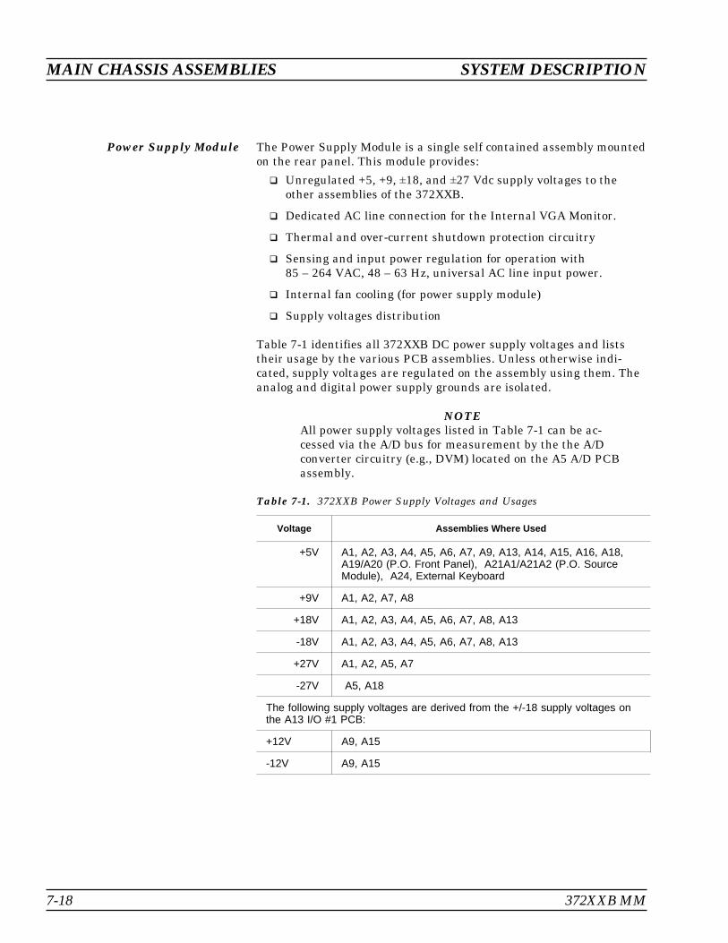
Power Supply Module The Power Supply Module is a single self contained assembly mountedon the rear panel. This module provides:
� Unregulated +5, +9, ±18, and ±27 Vdc supply voltages to theother assemblies of the 372XXB.
� Dedicated AC line connection for the Internal VGA Monitor.
� Thermal and over-current shutdown protection circuitry
� Sensing and input power regulation for operation with85 – 264 VAC, 48 – 63 Hz, universal AC line input power.
� Internal fan cooling (for power supply module)
� Supply voltages distribution
Table 7-1 identifies all 372XXB DC power supply voltages and liststheir usage by the various PCB assemblies. Unless otherwise indi-cated, supply voltages are regulated on the assembly using them. Theanalog and digital power supply grounds are isolated.
NOTEAll power supply voltages listed in Table 7-1 can be ac-cessed via the A/D bus for measurement by the the A/Dconverter circuitry (e.g., DVM) located on the A5 A/D PCBassembly.
MAIN CHASSIS ASSEMBLIES SYSTEM DESCRIPTION
7-18 372XXB MM
Voltage Assemblies Where Used
+5V A1, A2, A3, A4, A5, A6, A7, A9, A13, A14, A15, A16, A18,A19/A20 (P.O. Front Panel), A21A1/A21A2 (P.O. SourceModule), A24, External Keyboard
+9V A1, A2, A7, A8
+18V A1, A2, A3, A4, A5, A6, A7, A8, A13
-18V A1, A2, A3, A4, A5, A6, A7, A8, A13
+27V A1, A2, A5, A7
-27V A5, A18
The following supply voltages are derived from the +/-18 supply voltages onthe A13 I/O #1 PCB:
+12V A9, A15
-12V A9, A15
Table 7-1. 372XXB Power Supply Voltages and Usages
Internal VGA Monitor The internal monitor assembly is powered from a dedicated AC Linefrom the Power Supply Module. The degaussing and brightness con-trols for the internal monitor are located on the rear panel for easy ac-cess by the operator. There are no internal adjustments for this unit.
NOTEThe internal monitor assembly is not a field repairableunit.
SYSTEM DESCRIPTION MAIN CHASSIS ASSEMBLIES
372XXB MM 7-19/7-20

Table of Contents8-1 INTRODUCTION · · · · · · · · · · · · · · · · · · · · · · · · · 8-3
8-2 EQUIPMENT REQUIRED · · · · · · · · · · · · · · · · · · · · 8-3
8-3 REMOVE / REPLACE 372XXB COVERS · · · · · · · · · · · · 8-4
8-4 REMOVE / REPLACE THE A1–A9 ANDA13–A16 PCBS · · · · · · · · · · · · · · · · · · · · · · · · · · 8-6A1 – A9 PCBs · · · · · · · · · · · · · · · · · · · · · · · · · · · 8-6A13 – A16 PCB’s · · · · · · · · · · · · · · · · · · · · · · · · · · 8-6
8-5 REMOVE / REPLACE A9 PCB BBRAM CHIP· · · · · · · · · · 8-8
8-6 REMOVE / REPLACE A9 PCB SRAM BATTERY · · · · · · · 8-10
8-7 REMOVE / REPLACE A24 VME BUSTERMINATOR PCB · · · · · · · · · · · · · · · · · · · · · · · 8-12
8-8 REMOVE / REPLACE FRONT PANELASSEMBLY· · · · · · · · · · · · · · · · · · · · · · · · · · · · 8-13
8-9 REMOVE / REPLACE VGA DISPLAY MONITOR · · · · · · · 8-14
8-10 REMOVE / REPLACE LIQUID CRYSTALDISPLAY (LCD) · · · · · · · · · · · · · · · · · · · · · · · · · 8-16
8-11 REMOVE / REPLACE FLOPPY DISK DRIVE · · · · · · · · · 8-17
8-12 REMOVE / REPLACE REAR PANEL ASSEMBLY · · · · · · 8-19
8-13 REMOVE / REPLACE FAN ASSEMBLY · · · · · · · · · · · · 8-21
8-14 REMOVE / REPLACE POWER SUPPLYMODULE · · · · · · · · · · · · · · · · · · · · · · · · · · · · · 8-21
8-15 REMOVE / REPLACE A18 REAR PANEL PCB · · · · · · · · 8-22
Chapter 8Remove and ReplaceProcedures

8-16 REMOVE / REPLACE TEST SET MODULEASSEMBLIES · · · · · · · · · · · · · · · · · · · · · · · · · · 8-25Transfer Switch· · · · · · · · · · · · · · · · · · · · · · · · · · 8-25Input Coupler(s)/Low Freq Bridge(s) · · · · · · · · · · · · · · 8-26Power Amplifier · · · · · · · · · · · · · · · · · · · · · · · · · 8-26Buffer Amplifier/Sampler(A31) · · · · · · · · · · · · · · · · · 8-27Switched Doubler Module Assembly· · · · · · · · · · · · · · · 8-28
8-17 REMOVE / REPLACE SIGNAL SOURCEMODULE ASSEMBLIES · · · · · · · · · · · · · · · · · · · · 8-29Removal of Signal Source Module · · · · · · · · · · · · · · · · 8-29A21A2 Source Control PCB · · · · · · · · · · · · · · · · · · · 8-31A21A1 Source YIG Bias Control PCB · · · · · · · · · · · · · · 8-32Switched Filter Assembly · · · · · · · · · · · · · · · · · · · · 8-33Down Converter Assembly · · · · · · · · · · · · · · · · · · · · 8-33YIG Oscillator Assembly · · · · · · · · · · · · · · · · · · · · · 8-34

Chapter 8Remove and ReplaceProcedures
8-1 INTRODUCTION This chapter provides procedures for removing and replacing 372XXBfield exchangeable assemblies and components. When using these pro-cedures, please observe the warning and caution notices below.
WARNINGHazardous voltages are present inside the instrumentwhen ac line power is connected. Turn off the instrumentand remove the line cord before removing any covers orpanels.
CAUTIONMany assemblies in the 372XXB contain static-sensitivecomponents. Improper handling of these assemblies mayresult in damage to the assemblies. Always observe thestatic-sensitive component handling precautions describedin Chapter 1, Figure 1-2.
8-2 EQUIPMENT REQUIRED All procedures in this chapter require the use of either a #1 or #2 sizePhillips type screw driver. Any additional tool requirements are speci-fied at the beginning of each procedure.
372XXB MM 8-3
8-3 COVERS Adjustment and troubleshooting operations require removal of the topcover. Replacement of some 372XXB assemblies and parts require re-moval of all covers. The following procedures describe this process.
NOTEIt is only necessary to loosen the 372XXB handle assem-blies to remove the top, bottom, or side covers. However, ifthe front panel is to be removed, remove the handle as-semblies at this time.
Preliminary:
� Switch the 372XXB power off. Remove the power cord.
Procedure:
Step 1. Loosen (or remove) the right and left handle assemblies, asfollows:
� Place the 372XXB on its top (bottom-side up).
� Loosen/remove the screws at the sides of the handle as-semblies.
� If removing handles, pull them away from unit and setaside.
CAUTION
The green headed screws have Metricthreads.
Step 2. To remove the top cover:
� Place the 372XXB in normal (top-side up) position.
� Remove the feet from the two top corners at the rear ofthe 372XXB (Figure 7-1).
� Remove the center screw from rear of the top cover.
� Lift and slide the top cover away from the 372XXB.
Step 3. To remove the bottom cover:
� Place the 372XXB on its top (bottom-side up).
� Remove the feet from the two bottom corners at the rearof the 372XXB.
� Remove the center screw from rear of the bottom cover.
� Lift and slide the top cover away from the 372XXB.
Step 4. To remove the left cover:
COVERS REMOVE AND REPLACE
8-4 372XXB MM
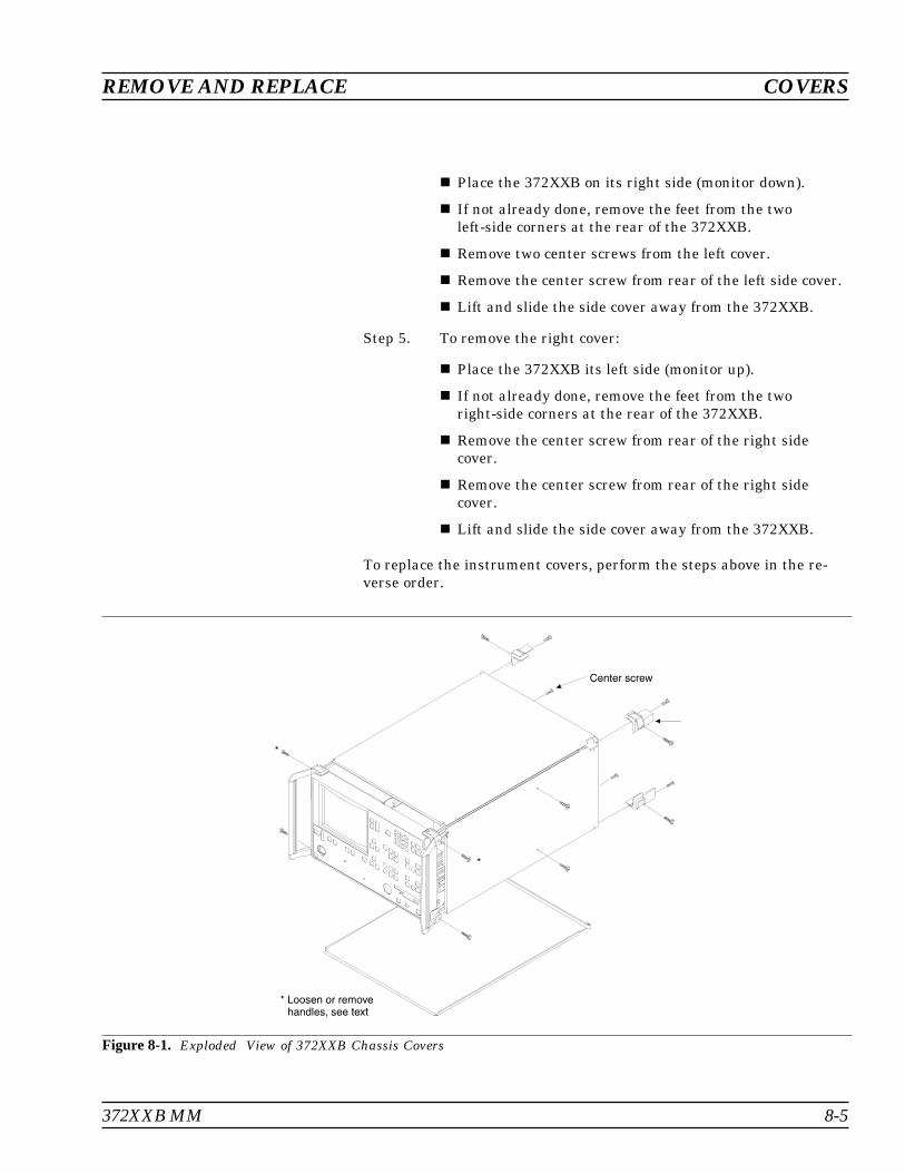
� Place the 372XXB on its right side (monitor down).
� If not already done, remove the feet from the twoleft-side corners at the rear of the 372XXB.
� Remove two center screws from the left cover.
� Remove the center screw from rear of the left side cover.
� Lift and slide the side cover away from the 372XXB.
Step 5. To remove the right cover:
� Place the 372XXB its left side (monitor up).
� If not already done, remove the feet from the tworight-side corners at the rear of the 372XXB.
� Remove the center screw from rear of the right sidecover.
� Remove the center screw from rear of the right sidecover.
� Lift and slide the side cover away from the 372XXB.
To replace the instrument covers, perform the steps above in the re-verse order.
REMOVE AND REPLACE COVERS
372XXB MM 8-5
Figure 8-1. Exploded View of 372XXB Chassis Covers

8-4 A1–A9/A13–A16 PCBS This paragraph provides instructions for removing and replacing theA1– A9 and A13 – A16 PCB’s, which are located underneath the cov-ers of the large and small card-cages, respectively.
Preliminary:
� Switch the 372XXB power off. Remove the power cord.
Remove the top cover (paragraph 8-3).
A1 – A9 PCBs
Procedure:
Step 1. Place the 372XXB in normal (top-side up) position.
Step 2. Remove the two screws that secure the large card-cagecover (Figure 8-2).
Step 3. Remove the large card-cage cover and set aside.
Step 4. Lift up on the edge tabs of the selected PCB(s) and liftstraight up.
To replace the PCB(s) and covers, perform the steps above in the re-verse order.
A13 – A16 PCB’s
Procedure:
Step 1. Place the 372XXB in normal (top-side up) position.
Step 2. Remove the two screws that secure the large card-cagecover (Figure 8-2).
Step 3. Remove the large card-cage cover, then remove the smallcard-cage cover and set aside.
Step 4. Lift up on the edge tabs of the selected PCB(s) and liftstraight up.
To replace the PCB(s) and covers, perform the steps above in the re-verse order.
8-5 A9 PCB BBRAM CHIP This paragraph provides instructions for removing and replacing theBBRAM Chip located on the A9 Main Processor PCB assembly.
A1–A9/A13–A16 PCBS REMOVE AND REPLACE
8-6 372XXB MM

REMOVE AND REPLACE A9 PCB BBRAM CHIP
372XXB MM 8-7
A9 PCB Assembly
Printed Circuit BoardAssemblies, A1-A8
PCB Assemblies A13-A16
Figure 8-2. A1-A9 and A13-A16 PCB Assemblies Removal Diagram

Preliminary:
Before removing and replacing the BBRAM Chip it is necessary tosave the following calibration data to the hard disk: signal source Fre-quency, ALC, Source Lock Threshold, LO1 and LO2. Proceed as fol-lows:
Step 1. Press the Option Menu key (Enhancement key group) todisplay the OPTIONS menu (left).
Step 2. Select DIAGNOSTICS from the menu. Then select in se-quence: H/W CALIBRATIONS |DISK OPERATIONS|SAVE TO HARD DISK |HW_CAL.ALL.
NOTEAlso save the calibration data to floppy disk. Labelthe disk with calibration type (ALL), date, and sys-tem model and serial numbers. Set the copy protecttab on the disk. Properly safeguard the disk so thatit will be available for later use, as needed.
Step 3. Switch the 372XXB power off. Remove the power cord.
Remove/Replace Procedure:
Step 1. Remove the top cover and the large card-cage cover to ex-pose the A1 – A9 PCBs (refer to paragraph 8-3).
Step 2. Remove the A9 PCB from the unit.
Step 3. Locate and remove the BBRAM chip from the A9 PCB. SeeFigure 8-3.
Step 4. Replace the BBRAM chip on the A9 PCB.
Step 5. Reinstall the A9 PCB, the large card-cage cover, and thetop cover.
Step 6. Reconnect power cord. Switch 372XXB power on.
Post Replacement Procedure:
Recall the calibration data saved in the Preliminary step from thefloppy disk as follows:
Step 1. Insert the floppy disk with the previously saved SourceFrequency and ALC Calibrations Data in the 372XXBfloppy disk drive.
Step 2. Select DIAGNOSTICS from the menu (left). Then select insequence: H/W CALIBRATIONS |DISK OPERATIONS|RECALL CAL FROM FLOPPY DISK|HW_CAL.ALL.
A9 PCB BBRAM CHIP REMOVE AND REPLACE
8-8 372XXB MM
OPTIONS
TRIGGERS
REAR PANELOUTPUT
DIAGNOSTICS
MULTIPLE SOURCECONTROL
PRESS <ENTER>TO SELECT
DIAGNOSTICS
START SELF TEST
READ SERVICE LOG
INSTALLED OPTIONS
PERIPHERAL TESTS
TROUBLESHOOTING(FOR SERVICEONLY)
H/W CALIBRATIONS(FOR SERVICEONLY)
PRESS <ENTER> TOSELECT
HARDWARECALIBRATIONS(FOR SERVICE
ONLY)
LO1CALIBRATION
LO2CALIBRATION
SOURCE FREQUENCYCALIBRATION
SOURCE ALCCALIBRATION
DISK OPERATIONS
PREVIOUS MENU
PRESS <ENTER> TOSELECT
H/W CALIBRATIONSDISK OPERATIONS
SAVETO HARD DISK
SAVETO FLOPPY DISK
RECALLFROM HARD DISK
RECALLFROM FLOPPY DISK
DELETEFROM HARD DISK
DELETEFROM FLOPPY DISK
COPY FROM HARDTO FLOPPY DISK
COPY FROM FLOPPYTO HARD DISK
PREVIOUS MENU
PRESS <ENTER> TOSELECT

NOTEIf unable to recall calibrations from disk, you mustredo the calibration data described in the Prelimi-nary step on the preceeding page.
Step 3. Ensure the system sweeps several times without errors.
Step 4. Refer to Chapter 3, Operational Tests. Perform the follow-ing:
� Check the Service Log for any new errors. (Note that theservice log is non-volatile; it may contain error entriesfrom a previous problem or service operation.)
� Run the Self Test procedure.
� Refer to Chapter 5, Troubleshooting, if any system er-rors are reported.
REMOVE AND REPLACE A9 PCB BBRAM CHIP
372XXB MM 8-9
BBRAMChip
Figure 8-3. Location of BBRAM Chip on the A9 PCB
OPTIONS
TRIGGERS
REAR PANELOUTPUT
DIAGNOSTICS
MULTIPLE SOURCECONTROL
PRESS <ENTER>TO SELECT
DIAGNOSTICS
START SELF TEST
READ SERVICE LOG
INSTALLED OPTIONS
PERIPHERAL TESTS
TROUBLESHOOTING(FOR SERVICEONLY)
H/W CALIBRATIONS(FOR SERVICEONLY)
PRESS <ENTER> TOSELECT
HARDWARECALIBRATIONS(FOR SERVICE
ONLY)
LO1CALIBRATION
LO2CALIBRATION
SOURCE FREQUENCYCALIBRATION
SOURCE ALCCALIBRATION
DISK OPERATIONS
PREVIOUS MENU
PRESS <ENTER> TOSELECT
H/W CALIBRATIONSDISK OPERATIONS
SAVETO HARD DISK
SAVETO FLOPPY DISK
RECALLFROM HARD DISK
RECALLFROM FLOPPY DISK
DELETEFROM HARD DISK
DELETEFROM FLOPPY DISK
COPY FROM HARDTO FLOPPY DISK
COPY FROM FLOPPYTO HARD DISK
PREVIOUS MENU
PRESS <ENTER> TOSELECT
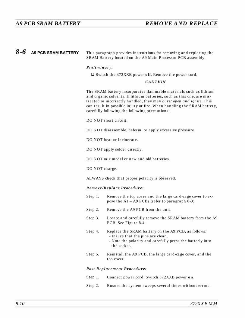
8-6 A9 PCB SRAM BATTERY This paragraph provides instructions for removing and replacing theSRAM Battery located on the A9 Main Processor PCB assembly.
Preliminary:
� Switch the 372XXB power off. Remove the power cord.
CAUTION
The SRAM battery incorporates flammable materials such as lithiumand organic solvents. If lithium batteries, such as this one, are mis-treated or incorrectly handled, they may burst open and ignite. Thiscan result in possible injury or fire. When handling the SRAM battery,carefully following the following precautions:
DO NOT short circuit.
DO NOT disassemble, deform, or apply excessive pressure.
DO NOT heat or incinerate.
DO NOT apply solder directly.
DO NOT mix model or new and old batteries.
DO NOT charge.
ALWAYS check that proper polarity is observed.
Remove/Replace Procedure:
Step 1. Remove the top cover and the large card-cage cover to ex-pose the A1 – A9 PCBs (refer to paragraph 8-3).
Step 2. Remove the A9 PCB from the unit.
Step 3. Locate and carefully remove the SRAM battery from the A9PCB. See Figure 8-4.
Step 4. Replace the SRAM battery on the A9 PCB, as follows:- Insure that the pins are clean.- Note the polarity and carefully press the batterly intothe socket.
Step 5. Reinstall the A9 PCB, the large card-cage cover, and thetop cover.
Post Replacement Procedure:
Step 1. Connect power cord. Switch 372XXB power on.
Step 2. Ensure the system sweeps several times without errors.
A9 PCB SRAM BATTERY REMOVE AND REPLACE
8-10 372XXB MM

Step 3. Refer to Chapter 3, Operational Tests. Perform the follow-ing:
� Check the Service Log for any new errors. (Note that theservice log is non-volatile; it may contain error entriesfrom a previous problem or service operation.)
� Run the Self Test procedure.
� Refer to Chapter 5, Troubleshooting, if any system er-rors are reported.
Step 4. Use front panel keys to set to Dual Channel Display 1 & 3.
Step 5. Save front panel setup to memory as follows:
� Press the Save/Recall Menu key
� Select SAVE from menu (top left): then in sequence se-lect: FRONT PANEL SETUP IN INTERNAL MEMORY|MEMORY 1
Step 6. Reset system to default settings by pressing the Defaultkey.
Step 7. Ensure the system resets to back to the defaultQuad-Channel display. Refer to Chapter 5, Trouble-shooting, if it does not.
Step 8. Recall the saved memory 1 setup as follows:
� Press the Save/Recall Menu key
� Select RECALL from menu (bottom left): then in se-quence select: FRONT PANEL SETUP IN INTERNALMEMORY |MEMORY 1
REMOVE AND REPLACE A9 PCB SRAM BATTERY
372XXB MM 8-11
SRAMBattery
Figure 8-4. Location of SRAM Battery on the A9 PCB
SAVE/RECALLFRONT PANELAND CAL DATA
SAVE
RECALL
PRESS <ENTER>TO SELECTFUNCTION
RECALL(OR SAVE)
FRONT PANELSETUP ININTERNAL MEMORY
FRONT PANELSETUP ANDCAL DATAON HARD DISK
FRONT PANELSETUP ANDCAL DATAON FLOPPY DISK
PRESS <ENTER>TO SELECT
SAVE FRONTPANEL SETUP TOINTERNAL MEMORY
MEMORY 1
MEMORY 2
MEMORY 3
MEMORY 4
MEMORY 5
MEMORY 6
MEMORY 7
MEMORY 8
MEMORY 9
MEMORY 10
PREVIOUS MENU
PRESS <ENTER>TO SELECT
ORUSE KEYPAD
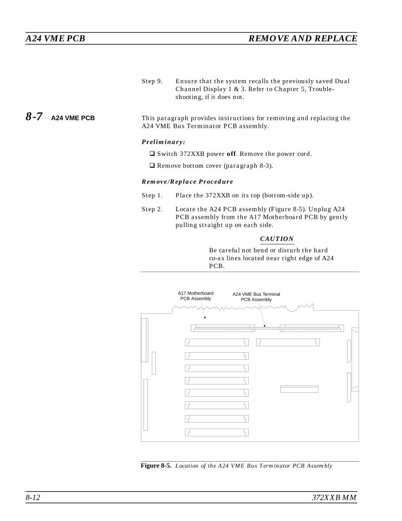
Step 9. Ensure that the system recalls the previously saved DualChannel Display 1 & 3. Refer to Chapter 5, Trouble-shooting, if it does not.
8-7 A24 VME PCB This paragraph provides instructions for removing and replacing theA24 VME Bus Terminator PCB assembly.
Preliminary:
� Switch 372XXB power off. Remove the power cord.
� Remove bottom cover (paragraph 8-3).
Remove/Replace Procedure
Step 1. Place the 372XXB on its top (bottom-side up).
Step 2. Locate the A24 PCB assembly (Figure 8-5). Unplug A24PCB assembly from the A17 Motherboard PCB by gentlypulling straight up on each side.
CAUTION
Be careful not bend or disturb the hardco-ax lines located near right edge of A24PCB.
A24 VME PCB REMOVE AND REPLACE
8-12 372XXB MM
A24 VME Bus TerminalPCB Assembly
A17 MotherboardPCB Assembly
Figure 8-5. Location of the A24 VME Bus Terminator PCB Assembly

8-8 FRONT PANELASSEMBLY
This paragraph provides instructions for removing and replacing the372XXB Front Panel assembly.
Equipment Required:
� Open-end wrench, 1 in.
Preliminary:
� Switch 372XXB power off. Remove the power cord.
� Remove handle assembles and all covers (paragraph 8-3).
Remove/Replace Procedure:
Step 1. Place the 372XXB in normal (top-side up) position.
Step 2. Remove the four corner screws and the top center screwthat secure the front panel assembly to the chassis (seeFigure 8-6).
Step 3. Place the 372XXB on its top (bottom-side up).
Step 4. Remove the screw that fastens the front panel casting ex-tension lip to the Test Set Module tray. (See diagram atleft.)
REMOVE AND REPLACE FRONT PANEL ASSEMBLY
372XXB MM 8-13
Figure 8-6. Removal of Front Panel Assembly

Step 5. Using a 1 in. open-end wrench, remove the nuts and wash-ers that secure the Port 1 and Port 2 couplers/bridges tothe front panel casting.
Step 6. Locate the cable from the front panel Power switch to con-nector J20 on the A17 Motherboard PCB. Disconnect atA17, J20 end.
Step 7. Locate the cable from the front panel Keyboard interfaceconnector to connector J16 on the A17 Motherboard PCB.Disconnect at A17, J16 end.
Step 8. Locate the cables from the front panel Bias Input BNC con-nectors to connector P2 on the A18 Rear Panel PCB. Dis-connect at A18, P2 end. (A18, P2 is the connector nearest tothe bottom lip of the rear panel.)
Step 9. Gently pull front panel assembly several inches away fromchassis. Locate cable from A17 Motherboard PCB to con-nector J1 on A20 Front Panel PCB. Disconnect at A20, J1end.
Step 10. Separate the bias input cables (Step 8) from the cable har-nesses, as necessary for removal. Pull front panel assemblyfree and set aside.
To replace the front panel assembly, perform the steps above in the re-verse order.
8-9 VGA MONITOR This paragraph provides instructions for removing and replacing theinternal VGA Display Monitor assembly.
NOTEIt is not necessary to remove the front panel assembly toperform this procedure.
Preliminary:
� Switch 372XXB power off. Remove the power cord.
� Remove all covers (paragraph 8-3).
Remove/Replace Procedure:
Step 1. Place the 372XXB on its right side (monitor down).
Step 2. At rear of monitor assembly, disconnect:
� The power cord (from the Power Supply Module)
� The data cable from motherboard CRT connector, J14
VGA MONITOR REMOVE AND REPLACE
8-14 372XXB MM

� The two cables from motherboard BRITE/DEGAUSSconnector, J15.
NOTEAll the the cables mentioned above have keyed con-nectors.
Step 3. Remove the four screws that fasten the monitor assemblyto the chassis (see Figure 8-7). Do not unfasten the screwwith the blue plastic washer under the screw head.
Step 4. Gently move the monitor assembly to the rear and liftaway from chassis, with cables still attached. Place onwork surface next to unit.
To replace the Internal VGA Display Monitor assembly, perform thesteps above in the reverse order.
REMOVE AND REPLACE VGA MONITOR
372XXB MM 8-15
J7
J2
TEST ATEST A
TEST BTEST B
J1
TP4
TP1
J2
TEST ATEST A
TEST BTEST B
J1
TP4
TP1
2 PL
2 PL
Figure 8-7. Location of Internal VGA Monitor Assembly Mounting Screws
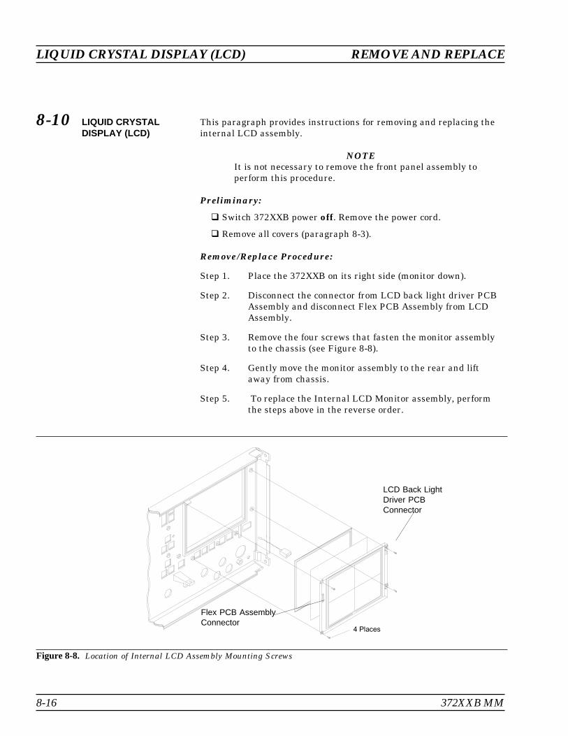
8-10 LIQUID CRYSTALDISPLAY (LCD)
This paragraph provides instructions for removing and replacing theinternal LCD assembly.
NOTEIt is not necessary to remove the front panel assembly toperform this procedure.
Preliminary:
� Switch 372XXB power off. Remove the power cord.
� Remove all covers (paragraph 8-3).
Remove/Replace Procedure:
Step 1. Place the 372XXB on its right side (monitor down).
Step 2. Disconnect the connector from LCD back light driver PCBAssembly and disconnect Flex PCB Assembly from LCDAssembly.
Step 3. Remove the four screws that fasten the monitor assemblyto the chassis (see Figure 8-8).
Step 4. Gently move the monitor assembly to the rear and liftaway from chassis.
Step 5. To replace the Internal LCD Monitor assembly, performthe steps above in the reverse order.
LIQUID CRYSTAL DISPLAY (LCD) REMOVE AND REPLACE
8-16 372XXB MM
4 Places
Figure 8-8. Location of Internal LCD Assembly Mounting Screws
LCD Back LightDriver PCBConnector
Flex PCB AssemblyConnector

8-11 LCD BACKLIGHTLAMP
This paragraph provides instructions for the removal and replacementof the LCD Backlight Lamp, which is recommended at approximately10,000 hours of operation, or if the display becomes dim.
NOTEThe front panel assembly does not have to be removed.
Preliminary:
� Switch 372XXB power off. Remove the power cord.
� Remove all covers (paragraph 8-3).
Remove/Replace Procedure:
Step 1. Remove the LCD assembly (paragraph 8-10).
Step 2. Remove the Backlight Lamp cover as follows:
On Sharp LQ9D169 LCD displays, remove the three Phil-lips screws on the side opposite the PCB, then lift off thecover.
On Sharp LQ9D340 LCD displays, on the side opposite thePCB, remove the tape covering the center catch. Starting atone end, very carefully push each catch clear of its tabwhile gently lifting the cover. Release all five catches andremove the cover.
Step 3. Replace the Backlight Lamp. Use care not to apply pres-sure to the area where the glass tube and the end caps ofthe Backlight Lamp meet.
Step 4. Reinstall the Backlight Lamp cover.
Step 5. Reinstall the LCD Assembly and reconnect electrical con-nectors.
Step 6. Reinstall the top cover.
Step 7. Turn the instrument on. Adjust the Brightness Potentiome-ter at the rear panel for maximum display brightness.
8-12 FLOPPY DISK DRIVE This paragraph provides instructions for removing and replacing theFloppy Disk Drive assembly.
NOTEIt is not necessary to remove the front panel assem-bly to perform this procedure.
REMOVE AND REPLACE LCD BACKLIGHT LAMP
372XXB MM 8-17
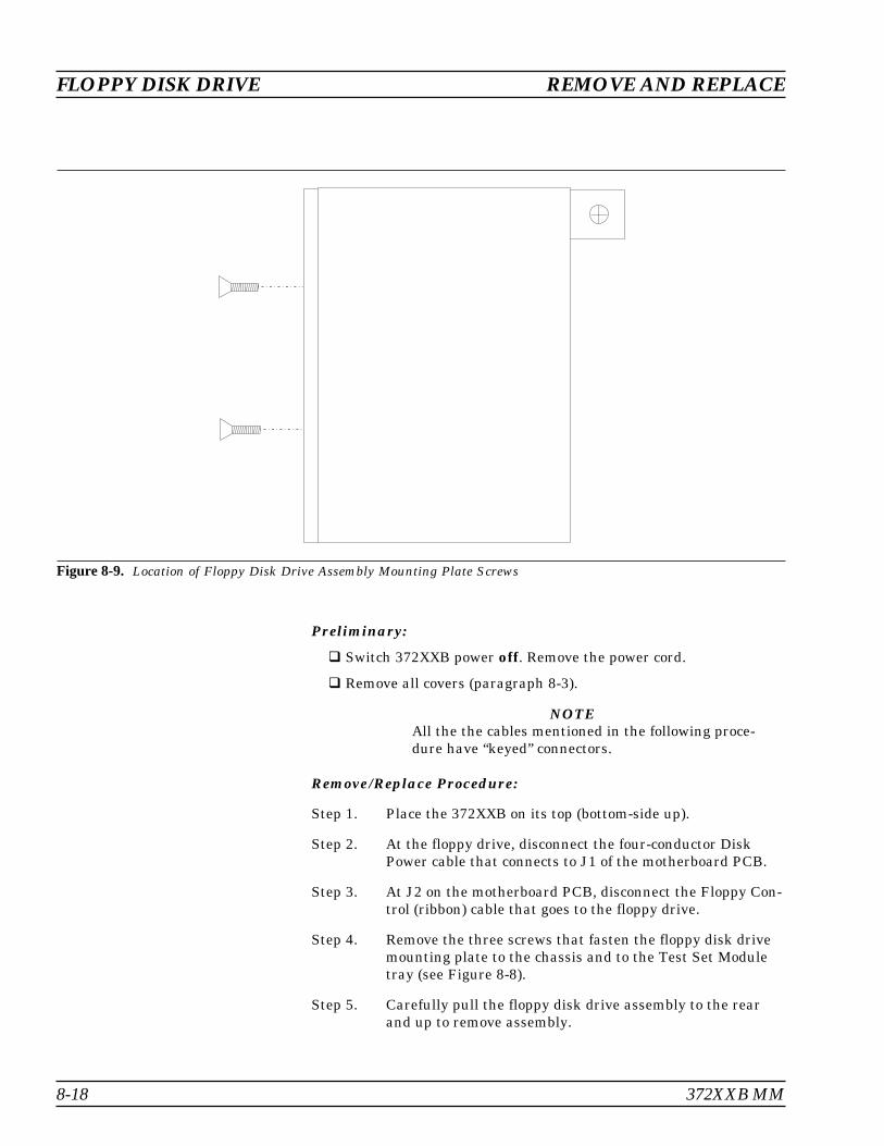
Preliminary:
� Switch 372XXB power off. Remove the power cord.
� Remove all covers (paragraph 8-3).
NOTEAll the the cables mentioned in the following proce-dure have “keyed” connectors.
Remove/Replace Procedure:
Step 1. Place the 372XXB on its top (bottom-side up).
Step 2. At the floppy drive, disconnect the four-conductor DiskPower cable that connects to J1 of the motherboard PCB.
Step 3. At J2 on the motherboard PCB, disconnect the Floppy Con-trol (ribbon) cable that goes to the floppy drive.
Step 4. Remove the three screws that fasten the floppy disk drivemounting plate to the chassis and to the Test Set Moduletray (see Figure 8-8).
Step 5. Carefully pull the floppy disk drive assembly to the rearand up to remove assembly.
FLOPPY DISK DRIVE REMOVE AND REPLACE
8-18 372XXB MM
Figure 8-9. Location of Floppy Disk Drive Assembly Mounting Plate Screws

Step 6. Carefully remove the Floppy Control cable from the rear ofthe floppy drive. Set aside for re-use.
To replace the Floppy Disk Drive assembly, perform the steps above inthe reverse order.
8-13 REAR PANELASSEMBLY
This paragraph provides instructions for removing and replacing theRear Panel Assembly.
Equipment Required Option 11 only):
� Connector torque wrench (516 in), ANRITSU Model 01-201, or
equivalent.
Preliminary:
� Switch 372XXB power off. Remove the power cord.
� Remove all covers (paragraph 8-3).
Remove/Replace Procedure:
Step 1. Place the 372XXB in normal (top-side up) position.
REMOVE AND REPLACE REAR PANEL ASSEMBLY
372XXB MM 8-19
External I/O
Reference Extension
RA In RB In RB Out
Display
IEEE 488.2 GPIB
10 MHz Ref
� ExtTrigger
ExtAnlg In
100-120V 5A SB
SAME TYPE AND RATING
85-264VAC48-63HzREPLACE FUSE ONLY WITH
540VA MAX
220-240V 2.5A SB
Bias FusesPort 1 Port 2
VGA OUT
Printer Out
CRT Degauss CRT Brt
WARNINGNO OPERATOR SERVICE-ABLE PARTS INSIDEREFER SERVICING TO
QUALIFIED PERSONNEL
CAUTIONFOR CONTINUED FIREPROTECTION REPLACEONLY WITH SPECIFIEDTYPE AND RATED FUSE
SH
1
AH
1
T6
L4
SR
1
RL
1
PP
1
DC
1
DT
1
C0
E2
Refer to manualfor GPIB address
RAOutFUSE
FUSEFU
SE
FUSE
FUSEFU
SE
1n ±5dBm 50 Out 0dBm 50
ExtAnlg Out
1
24 PL
1
13 3
4
Rear Panel Assembly screws (par 8-11)Fan Assembly screws (par 8-12)Power Supply Assembly screws (par 8-13)A18 Rear Panel PCB screw (par 8-14)
1234
Figure 8-10. Location of Mounting Screws for Rear Panel Assemblies

Step 2. Remove the three screws on each side of the chassis thatfasten to the rear panel assembly. See Figure 8-10.
Step 3. Remove the two screws located near top and middle of rearpanel (near fan-mounting screws). See Figure 8-10.
Step 4. Locate cable from the rear-panel 10 MHz Ref In BNC con-nector to connector J2 of A7 PCB. Disconnect at A7, J2 end.(Pull up gently to disconnect.)
Step 5. Locate cable from the rear-panel 10 MHz Ref Out BNCconnector to connector J3 of A7 PCB. Disconnect at A7, J3end.
Step 6. Locate cable from the rear-panel Ext Anlg In BNC connec-tor to connector J1 of A5 PCB. Disconnect at A5, J1 end.
Step 7. Place the 372XXB on its right side (monitor down).
Step 8. Locate the cables from the rear-panel Ext Trigger and ExtAnlg Out BNC connectors to connector P13 of the A18 RearPanel PCB. Disconnect at A18, P13 end. (A18, P3 is thefourth connector away from the rear panel bottom lip.)
Step 9. Disconnect the large ribbon cable from connector P1 of theA18 PCB at motherboard connector J12.
Step 10. Disconnect the two cables from the Power Supply Moduleat motherboard connectors J4 and J13.
Step 11. Disconnect power cord from the Power Supply Module tothe internal VGA Display Monitor at the display monitor.
Step 12. If 372XXB is equipped with Option 11, Reference Loop Ex-tension Cables:
� Using a 516 in. wrench, disconnect the external cable
Loops from the rear panel connectors.
� Using a 516 in. wrench, disconnect the semi-rigid coaxial
lines W141 and W145 at the inside of the rear panel. SeeFigure 8-11 on page 8-23.
Step 13. If 372XXB is equipped with Option 10, High Stability TimeBase:
� Locate output cable from the high stability oscillator as-sembly (mounted above Power supply Module) to connec-tor J1 of A7 PCB. Disconnect at A7, J1 end.
� Locate power cable from the high stability oscillator as-sembly to A17 Motherboard connector, J18. Disconnectat A17, J18 end.
REAR PANEL ASSEMBLY REMOVE AND REPLACE
8-20 372XXB MM

Step 14. Place the 372XXB in normal (top-side up) position. Gentlypull rear panel assembly away from chassis and lay flat onwork surface. Remove cables from cable harnesses, as re-quired.
To replace the Rear Panel Assembly, perform the steps above in thereverse order.
8-14 FAN ASSEMBLY This paragraph provides instructions for removing and replacing theRear Panel Fan Assembly.
Preliminary:
� Switch 372XXB power off. Remove the power cord.
� Remove all covers (paragraph 8-3).
� Remove Rear Panel (paragraph 8-12).
Remove/Replace Procedure:
Step 1. Place the Rear Panel Assembly on the work surface withthe A18 Rear Panel PCB up.
Step 2. Disconnect the two conductor fan power cable at connectorP6 of the A18 PCB.
Step 3. Turn Rear Panel Assembly over, and remove the fourscrews that fasten the fan guard and fan assembly to therear panel. See Figure 8-10.
Step 4. Remove the fan guard and separate the fan from the rearpanel.
To replace the Rear Panel Fan Assembly, perform the steps above inthe reverse order.
8-15 POWER SUPPLYMODULE
This paragraph provides instructions for removing and replacing thePower Supply Module.
Preliminary:
� Switch 372XXB power off. Remove the power cord.
� Remove all covers (paragraph 8-3).
� Remove Rear Panel (paragraph 8-12).
Remove/Replace Procedure:
Step 1. Place the Rear Panel Assembly on the work surface withthe Power Supply Module down.
REMOVE AND REPLACE FAN ASSEMBLY
372XXB MM 8-21

Step 2. Remove the six screws from the rear panel that fasten it tothe left and right edges of the Power Supply Module (seeFigure 8-10). Gently separate the two units.
To replace the Power Supply Module, perform the steps above in thereverse order.
8-16 A18 REAR PANEL PCB This paragraph provides instructions for removing and replacing theA18 Rear Panel PCB assembly.
Equipment Required:
� Nut Driver, 932 in.
� Nut Driver, 316 in.
Preliminary:
� Switch 372XXB power off. Remove the power cord.
� Remove all covers (paragraph 8-3).
� Remove Rear Panel (paragraph 8-12).
Remove/Replace Procedure:
Step 1. Place the Rear Panel Assembly on the work surface withthe A18 Rear Panel PCB up.
Step 2. Disconnect the two-conductor fan power cable at connectorP6 of the A18 PCB.
Step 3. Disconnect the wiring for the rear panel Bias Fuses at con-nector P4 of the A18 PCB.
Step 4. Turn Rear Panel Assembly over. Remove screw located atlower left corner of the rear panel that fastens the A18PCB to the Rear Panel Assembly (see Figure 8-10).
Step 5. Using a 932 in. nut driver, remove the standoffs that fasten
the IEEE 488.2 GPIB and Dedicated GPIB connectors tothe rear panel.
Step 6. Using a 316 in. nut driver, remove the standoffs that fasten
the Printer Out, VGA Out, and External/IO connectorsto the rear panel. Set standoffs aside for re-use.
Step 7. Carefully separate the A18 PCB from the rear panel.
To replace the A18 Rear Panel PCB assembly, perform the steps abovein the reverse order.
A18 REAR PANEL PCB REMOVE AND REPLACE
8-22 372XXB MM
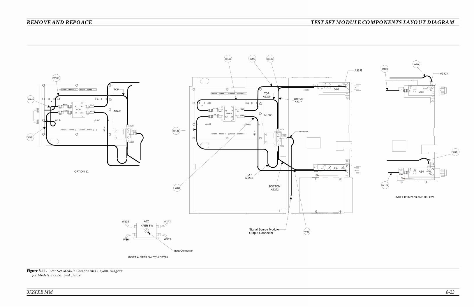
372XXB MM 8-23
REMOVE AND REPOACE TEST SET MODULE COMPONENTS LAYOUT DIAGRAM
Signal Source ModuleOutput Connector
A33J3A33J3
J8
J8
J10
J10
J9
J9
A31J9
A31J9
A33J2
A33J3
A33J3
A31J11
A31J11
A32J1
A32J1A32J3
A32J3
A32J2
A32J2
A34J2
A34J2
A34J3
A34J3
A31J10
A31J10
A31J8
A31J8
J11
J11
A32
A32
J1
J1
J2
J2
J3
J3
A33A33
J1
J1
J2
J2
J3
J3
J4
J4
A34A34J1
J1
J2
J2
J4
J4J3
J3
P/O A31
P/O A31
FROM A32J1
TOPA32J4
BOTTOMA32J2
TOPA32J5
TOP
A37J2
A37J2
W132
XFER SW
A32 W141
W123
Input Connector
INSET A: XFER SWITCH DETAIL
W86
OPTION 11
INSET B: 37217B AND BELOW
W90
W139
W109
W191
W86
W126
BOTTOMA32J3
W85W136
W132
W145
W141
W132
W88
Figure 8-11. Test Set Module Components Layout Diagramfor Models 37225B and Below

8-24 372XXB MM
TEST SET MODULE COMPONENTS LAYOUT DIAGRAM REMOVE AND REPOACE
W86Signal Source Module
Output Connector
W106
W81
A33J3
J8
J10
J9A31J9
A33J2
A33J3
A31J11
A32J1
A32J3
A32J2
A34J2
A34J3
A31J10
A31J8
J11
A32J1
J2
J3
A33J1J2
J3J4
A34J2
A34J1
J2
J4
J3
P/O A31
TOP
A32J2
(W86) BOTTOM
TOP
A37J2
W85W126
W147
W43
W132
W107
W141
W141
or
A36
Figure 8-12. Test Set Module Components Layout Diagramfor Model 37269B (with Options 6 and 11)
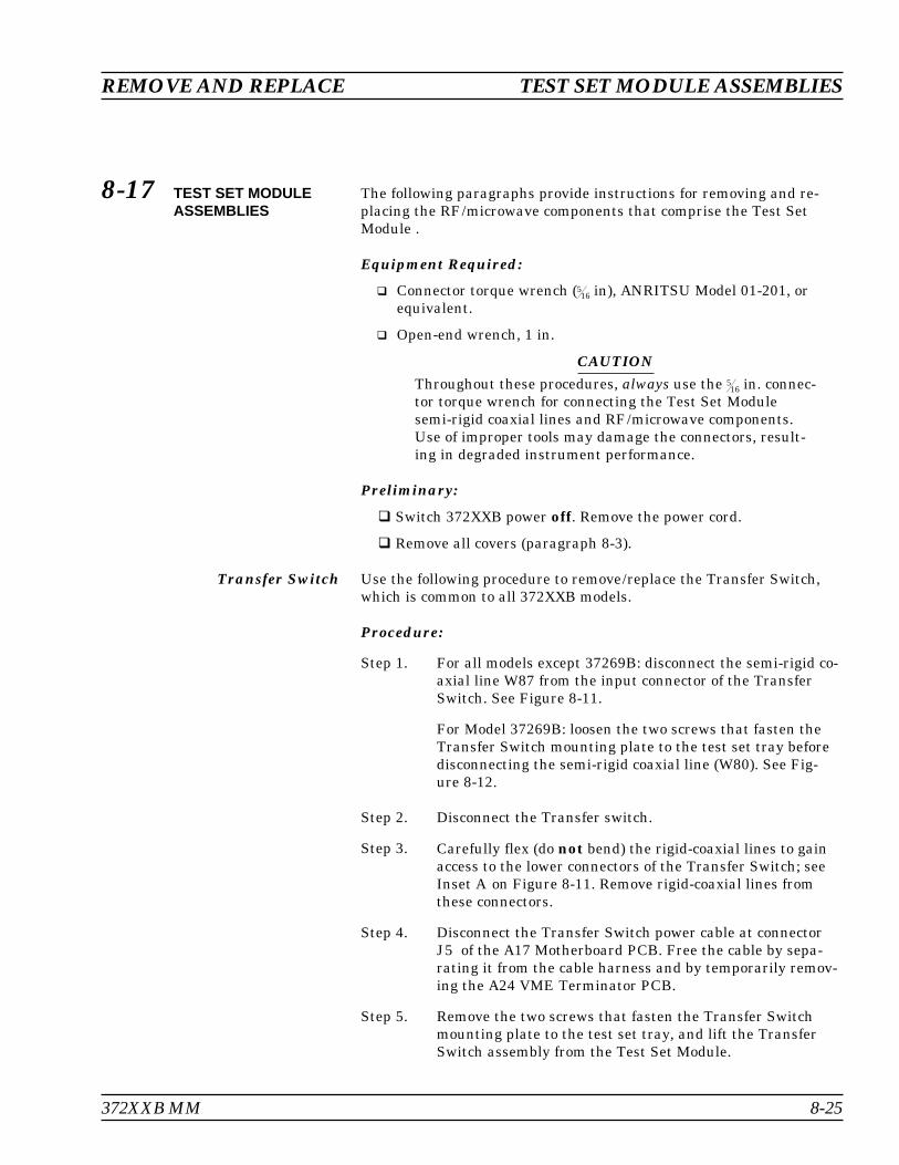
8-17 TEST SET MODULEASSEMBLIES
The following paragraphs provide instructions for removing and re-placing the RF/microwave components that comprise the Test SetModule .
Equipment Required:
� Connector torque wrench (516 in), ANRITSU Model 01-201, or
equivalent.
� Open-end wrench, 1 in.
CAUTIONThroughout these procedures, always use the 5
16 in. connec-tor torque wrench for connecting the Test Set Modulesemi-rigid coaxial lines and RF/microwave components.Use of improper tools may damage the connectors, result-ing in degraded instrument performance.
Preliminary:
� Switch 372XXB power off. Remove the power cord.
� Remove all covers (paragraph 8-3).
Transfer Switch Use the following procedure to remove/replace the Transfer Switch,which is common to all 372XXB models.
Procedure:
Step 1. For all models except 37269B: disconnect the semi-rigid co-axial line W87 from the input connector of the TransferSwitch. See Figure 8-11.
For Model 37269B: loosen the two screws that fasten theTransfer Switch mounting plate to the test set tray beforedisconnecting the semi-rigid coaxial line (W80). See Fig-ure 8-12.
Step 2. Disconnect the Transfer switch.
Step 3. Carefully flex (do not bend) the rigid-coaxial lines to gainaccess to the lower connectors of the Transfer Switch; seeInset A on Figure 8-11. Remove rigid-coaxial lines fromthese connectors.
Step 4. Disconnect the Transfer Switch power cable at connectorJ5 of the A17 Motherboard PCB. Free the cable by sepa-rating it from the cable harness and by temporarily remov-ing the A24 VME Terminator PCB.
Step 5. Remove the two screws that fasten the Transfer Switchmounting plate to the test set tray, and lift the TransferSwitch assembly from the Test Set Module.
REMOVE AND REPLACE TEST SET MODULE ASSEMBLIES
372XXB MM 8-25

To replace the Transfer Switch assembly, perform the steps above inthe reverse order. W111 for Models 37211B and 37217B
Input Coupler(s)/ LowFreq Bridge(s)
Use the following procedure to remove/replace the Input Coupler(s) ofall models 37225B through 37269B and the Low Frequency Bridges ofmodels 37211B and 37217B.
Procedure:
Step 1. Using a 1 in. open-end wrench, remove the front panel nutand washer of the Port1or Port2 coupler/bridge that is tobe removed.
Step 2. Disconnect the two semi-rigid coaxial lines associated withthe coupler/bridge (see Figure 8-11).
Step 3. Remove the two screws that fasten the coupler/bridgebracket to the test set tray. Move coupler/bridge to the rearand up to remove it from the Test Set Module.
To replace the coupler/bridge, perform the steps above in the reverseorder.
Power Amplifier Use the following procedure to remove/replace the Power Amplifier as-sembly, which is common to all 372XXB models.
Procedure:
Step 1. Disconnect the Power Amplifier power cable at connectorJ5 of the A17 Motherboard PCB. Free the cable by separat-ing it from the cable harness and by temporarily removingthe A24 VME Terminator PCB.
Step 2. Disconnect the PWR AMP IN cable on the side of the PowerAmplifier assembly; see Figure 8-13. (Pull out gently to dis-connect.)
Step 3. Remove the two screws that fasten the Power Amplifier as-sembly to the test set tray. Remove the two screws that fas-tens the assembly feet to the Buffer Amplifier/Sampler as-sembly.
Step 4. Disconnect the Power Amplifier from the BufferAmplifier/Sampler by carefully pulling up on the connectorend of the rigid-coaxial line from the Power Amplifier. (SeeFigure 8-13.) Carefully lift the assembly from the Test SetModule.
To replace the Power Amplifier assembly, perform the steps above inthe reverse order.
TEST SET MODULE ASSEMBLIES REMOVE AND REPLACE
8-26 372XXB MM
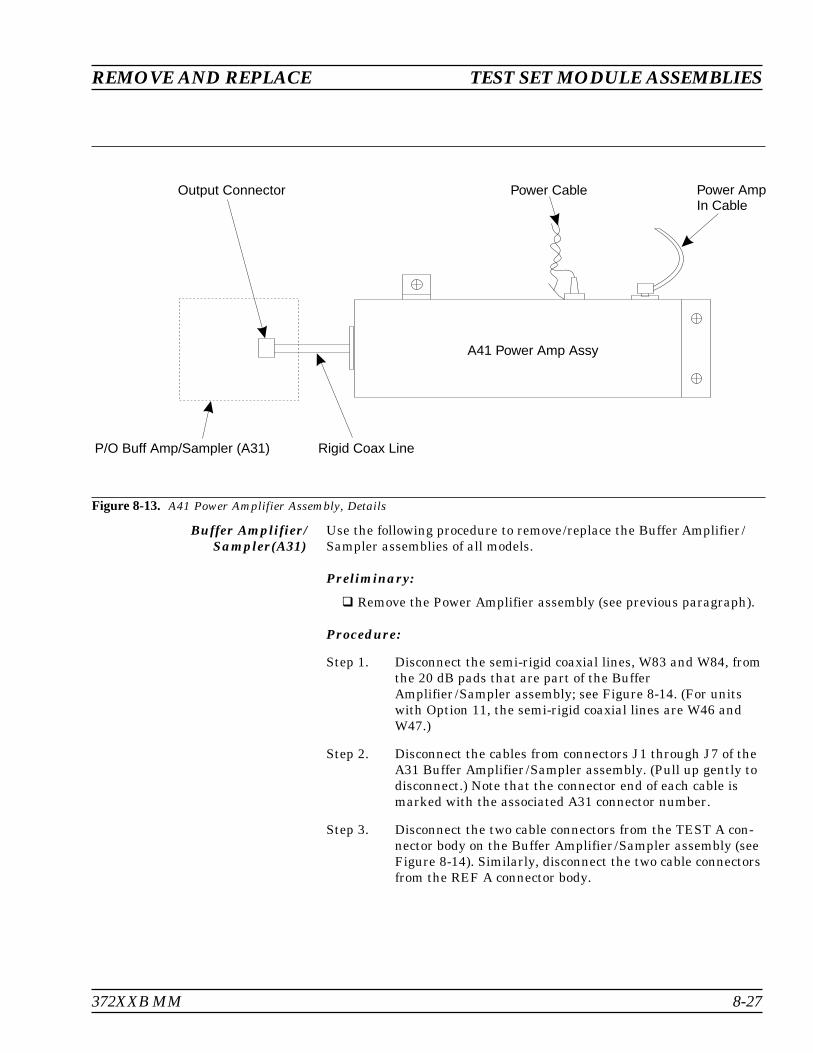
Buffer Amplifier/Sampler(A31)
Use the following procedure to remove/replace the Buffer Amplifier/Sampler assemblies of all models.
Preliminary:
� Remove the Power Amplifier assembly (see previous paragraph).
Procedure:
Step 1. Disconnect the semi-rigid coaxial lines, W83 and W84, fromthe 20 dB pads that are part of the BufferAmplifier/Sampler assembly; see Figure 8-14. (For unitswith Option 11, the semi-rigid coaxial lines are W46 andW47.)
Step 2. Disconnect the cables from connectors J1 through J7 of theA31 Buffer Amplifier/Sampler assembly. (Pull up gently todisconnect.) Note that the connector end of each cable ismarked with the associated A31 connector number.
Step 3. Disconnect the two cable connectors from the TEST A con-nector body on the Buffer Amplifier/Sampler assembly (seeFigure 8-14). Similarly, disconnect the two cable connectorsfrom the REF A connector body.
REMOVE AND REPLACE TEST SET MODULE ASSEMBLIES
372XXB MM 8-27
Power AmpIn Cable
Power CableOutput Connector
Rigid Coax Line
A41 Power Amp Assy
P/O Buff Amp/Sampler (A31)
Figure 8-13. A41 Power Amplifier Assembly, Details
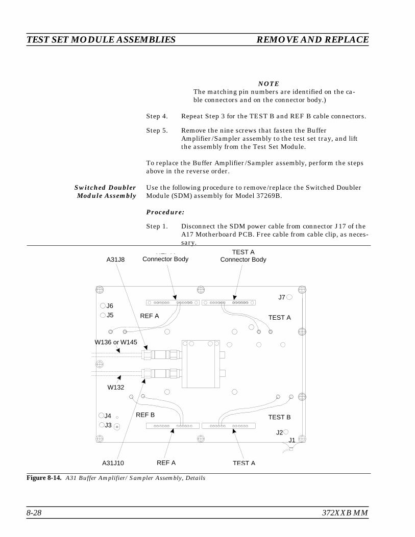
NOTEThe matching pin numbers are identified on the ca-ble connectors and on the connector body.)
Step 4. Repeat Step 3 for the TEST B and REF B cable connectors.
Step 5. Remove the nine screws that fasten the BufferAmplifier/Sampler assembly to the test set tray, and liftthe assembly from the Test Set Module.
To replace the Buffer Amplifier/Sampler assembly, perform the stepsabove in the reverse order.
Switched DoublerModule Assembly
Use the following procedure to remove/replace the Switched DoublerModule (SDM) assembly for Model 37269B.
Procedure:
Step 1. Disconnect the SDM power cable from connector J17 of theA17 Motherboard PCB. Free cable from cable clip, as neces-sary.
TEST SET MODULE ASSEMBLIES REMOVE AND REPLACE
8-28 372XXB MM
REF AConnector BodyA31J8
REF AA31J10
W132
J1J2
J3
J4
J5
J6J7
W136 or W145
REF A
REF B
TEST A
TEST B
TEST AConnector Body
TEST A
Figure 8-14. A31 Buffer Amplifier/Sampler Assembly, Details

Step 2. Disconnect the semi-rigid coaxial line W81 from the inputconnector of the SDM; see Figure 8-12.
Step 3. Remove the two screws that fasten the SDM to the Test SetModule tray.
Step 4. Disconnect the semi-rigid coaxial line W80 from the outputconnector of the SDM; see Figure 8-12. Carefully lift the as-sembly from the Test Set Module.
To replace the Switched Doubler Module assembly, perform the stepsabove in the reverse order.
8-18 SIGNAL SOURCEMODULES
The following paragraphs provide instructions for removing and re-placing the RF/microwave components that comprise the SignalSource Module. After replacement of any assembly in the Source Mod-ule, the following recalibrations should be performed:
� Frequency Calibration
� Port 1 ALC Calibration
� Port 2 ALC Calibration
� Source Lock Threshold (Model 37297B only)
Equipment Required:
� Connector torque wrench (516 in), ANRITSU Model 01-201, or
equivalent.
CAUTIONThroughout these procedures, always use the 5
16 in. connec-tor torque wrench for connecting the Signal Source Modulesemi-rigid coaxial lines and RF/microwave components.Use of improper tools may damage the connectors, result-ing in degraded instrument performance.
Preliminary:
� Switch 372XXB power off. Remove the power cord.
� Remove all covers (paragraph 8-3).
Removal of SignalSource Module
Use the following procedure to remove the Signal Source Module fromthe chassis. This step is necessary before any of the module compo-nents can be removed/replaced.
Procedure:
Step 1. Place the 372XXB on its top (bottom-side up).
Step 2. At J2 on the motherboard PCB, disconnect the Floppy Con-trol (ribbon) cable that goes to the floppy drive. Dress the
REMOVE AND REPLACE SIGNAL SOURCE MODULES
372XXB MM 8-29
ribbon cable away from the Signal Source Module outputconnector; see Figure 8-11.
Step 3. Disconnect the semi-rigid coaxial line W87* from the out-put connector of the Signal Source Module.
Step 4. Place the 372XXB in normal (top-side up) position.
Step 5. Disconnect the cables from connectors J1 and J2 of theA21A2 Source Control PCB. (Pull up gently to disconnect.)Note that the connector end of each cable is marked withthe associated A21A2 connector number.
Step 6. Disconnect the cable from connector J3** of the A21A2Source Control PCB. Dress cables away from the SignalSource Module.
Step 7. Remove the three screws that fasten the Signal SourceModule to the chassis side rail. See Figure 8-15.
Step 8. Loosen the two captive screws that fasten the SignalSource Module to the chassis (Figure 8-15).
Step 9. Pull up at the rear of the Signal Source Module to discon-nect the A21A1 Source YIG Bias Control PCB from the A17Motherboard PCB. Lift the module from the chassis andplace on work surface.
To replace the Signal Source Module, perform the steps above in thereverse order.
CAUTIONNever operate unit with J3 disconnected on A21A2 mod-ule. The transfer switch may be damaged by high RFpower.
SIGNAL SOURCE MODULES REMOVE AND REPLACE
8-30 372XXB MM
* W81 for Models 37269B** Never operate unit with A21A2, J3 discon-nected. Refer to Caution statement on

A21A2 Source ControlPCB
Use the following procedure to remove/replace the A21A2 Source Con-trol PCB assembly.
Procedure:
Step 1. Unfasten the two PCB retainers at the top corners of theA21A2 Source Control PCB (see Figure 8-16). To unfasten,turn screwdriver slot 1
4 turn counter-clockwise.
Step 2. Pull the top of the A21A2 PCB away from the source mod-ule chassis back plate to clear PCB retainers. Gently pullup to disconnect the A21A2 PCB from the socket on theA21A1 Source YIG Bias Control PC. Remove from SourceModule.
To replace the A21A2 Source Control PCB assembly, perform the stepsabove in the reverse order.
REMOVE AND REPLACE SIGNAL SOURCE MODULES
372XXB MM 8-31
Side Rail MountingScrews
Captive Screws
A21A2 SourceControl PCB
Figure 8-15. Signal Source Module Removal Details
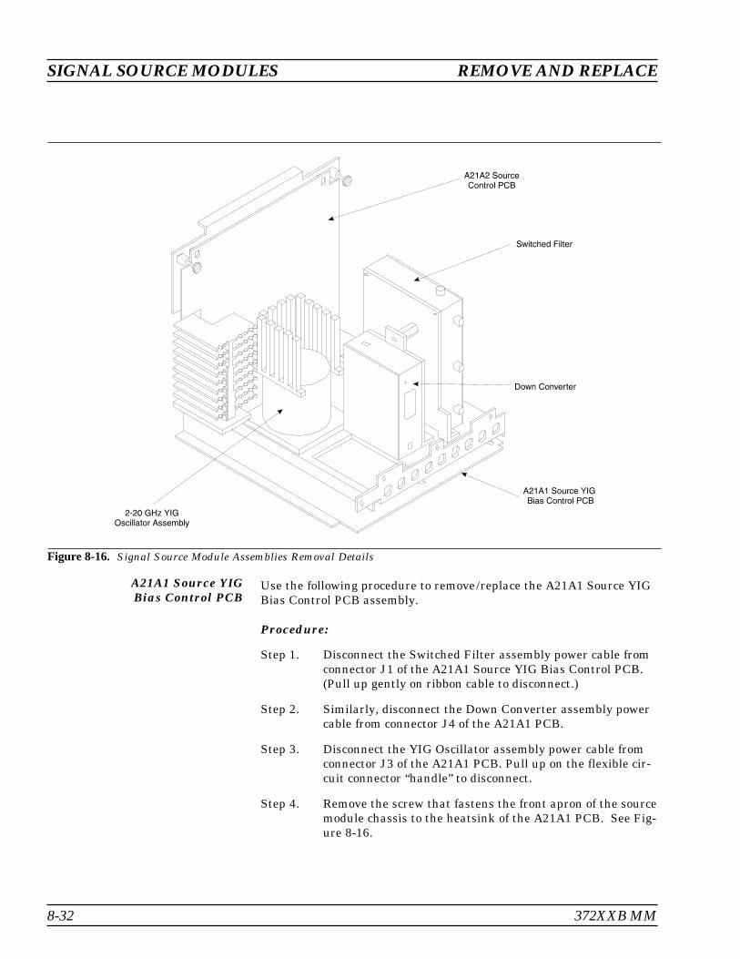
A21A1 Source YIGBias Control PCB
Use the following procedure to remove/replace the A21A1 Source YIGBias Control PCB assembly.
Procedure:
Step 1. Disconnect the Switched Filter assembly power cable fromconnector J1 of the A21A1 Source YIG Bias Control PCB.(Pull up gently on ribbon cable to disconnect.)
Step 2. Similarly, disconnect the Down Converter assembly powercable from connector J4 of the A21A1 PCB.
Step 3. Disconnect the YIG Oscillator assembly power cable fromconnector J3 of the A21A1 PCB. Pull up on the flexible cir-cuit connector “handle” to disconnect.
Step 4. Remove the screw that fastens the front apron of the sourcemodule chassis to the heatsink of the A21A1 PCB. See Fig-ure 8-16.
SIGNAL SOURCE MODULES REMOVE AND REPLACE
8-32 372XXB MM
Figure 8-16. Signal Source Module Assemblies Removal Details

Step 5. Remove the four screws that fastens the back plate of thesource module chassis to the heatsink of the A21A1 PCB.
Step 6. Place the Signal Source Module on its‘ back plate.
Step 7. Unfasten the six PCB retainers on the bottom of the A21A1PCB. (To unfasten, turn screwdriver slot 1
4 turn coun-ter-clockwise.) Gently separate the A21A1 PCB (includingthe heat sink) from the Signal Source Module.
To replace the A21A1 Source YIG Bias Control PCB assembly, per-form the steps above in the reverse order.
Switched FilterAssembly
Use the following procedure to remove/replace the Switched Filter as-sembly.
Procedure:
Step 1. Disconnect the power cable from connector P1 at the rear ofthe Switched Filter assembly. (Use a small screw driver topry up gently at each end of the connector, as necessary.)
Step 2. Disconnect the semi-rigid coaxial lines from connector J6(top) and connector J3 (lower-front) of the Switched Filterassembly.
Step 3. Disconnect the semi-rigid coaxial line from the RF INPUT(top) connector of the Down Converter assembly.
Step 4. Remove the two screws that fasten the Switched Filter as-sembly to the source module chassis and lift the assemblyfrom the Signal Source Module.
Step 5. Disconnect the semi-rigid coaxial line from connector J1(bottom) of the Switched Filter assembly. Put this coaxialline aside for re-use.
NOTEWhen replacing the Switched Filter assembly, con-nect the semi-rigid coaxial line to the bottom connec-tor (J1), before attaching the assembly to the SignalSource Module.
To replace the Switched Filter assembly, perform the steps above inthe reverse order.
Down ConverterAssembly
Use the following procedure to remove/replace the Down Converterassembly.
REMOVE AND REPLACE SIGNAL SOURCE MODULES
372XXB MM 8-33

Procedure:
Step 1. Disconnect the power cable from connector P1 at the frontof the Down Converter assembly.
Step 2. Disconnect the semi-rigid coaxial lines from the RF INPUTconnector and RF OUTPUT connector of the Down Con-verter assembly.
Step 3. Remove the two screws that fasten the Down Converter as-sembly to the source module chassis and lift the assemblyfrom the Signal Source Module.
To replace the Down Converter assembly, perform the steps above inthe reverse order.
YIG OscillatorAssembly
Use the following procedure to remove/replace the YIG Oscillator as-sembly.
Procedure:
Step 1. Disconnect the YIG Oscillator assembly power cable fromconnector J3 of the A21A1 PCB. Pull up on the flexible cir-cuit connector “handle” to disconnect.
Step 2. Disconnect the semi-rigid coaxial line from the connectorJ6 (top) of the Switched Filter assembly.
Step 3. Remove the four screws that fasten the YIG Oscillator as-sembly to the source module chassis and lift the assemblyfrom the Signal Source Module.
Step 4. Disconnect the semi-rigid coaxial line from the output con-nector of the YIG Oscillator assembly. Put this coaxial lineaside for re-use.
NOTEWhen replacing the YIG Oscillator assembly, con-nect the semi-rigid coaxial line removed in Step 4 tothe output connector of the YIG Oscillator before at-taching it to the Signal Source Module.
To replace the YIG Oscillator assembly, perform the steps above in thereverse order.
SIGNAL SOURCE MODULES REMOVE AND REPLACE
8-34 372XXB MM
Table of ContentsA-1 INTRODUCTION · · · · · · · · · · · · · · · · · · · · · · · · · A-3
A-2 DIAGNOSTICS MENUS · · · · · · · · · · · · · · · · · · · · · A-3
Appendix ADiagnostics Menus


Appendix ADiagnostics Menus
A-1 INTRODUCTION This appendix contains descriptions and usage information for the372XXB Diagnostic Menus that are available via the front panel Op-tion Menu key.
A-2 DIAGNOSTICS MENUS The internal diagnostic capabilities of the 372XXB are accessed viathe Options Menu key, which is part of the front panel Enhancementkey group. The selections available from the top level DIAGNOSTICSmenu (DG1) are listed below. See Figure A-1.
� Start Self Test
� Read Service Log
� Installed Options
� Peripheral Tests
� Troubleshooting
� H/W Calibrations
Start Self Test The START SELF TEST selection, when invoked, will automaticallytest circuits throughout the 372XXB. Once invoked, it requires no ex-ternal devices or interaction by the user. The net pass/fail result of theself-test is written to the CRT screen. Any self test failures will causedetailed failure information to be written into the service log.
This menu is available to service and non-service personnel.
Read Service Log The READ SERVICE LOG menu allows for viewing, printing, clear-ing, and saving the internal system service log to floppy disk. TheCLEAR LOG function is not recommended for non-service personnel.
The Service Log is made up of two parts, the log header and the errorlisting. The log header contains key system parameters such as initialsystem turn-on date/time/temperature, current power-on date/time/temperature, total operational hours, system model, serial, and in-stalled option numbers, date/time/temperature stamp of current ser-vice log viewing session, date/time/temperature of internal hardwarecalibrations, and statistics about various internal system phase lock-ing activities.
The error listing is a time ordered log containing the system faultswith details about the system condition at the time of the fault.
372XXB MM A-3

NOTEThe service log must always be printed out or saved todisk and sent to the factory along with a failed assembly.Due to the importance of the information provided by theservice log to ANRITSU factory Service Engineers, the ex-change prices are only valid if the service log data (disk orprintout) is submitted to the factory with the failed assem-bly.
This menu is available to service and non-service personnel. However,the service log should be cleared by service personnel only.
Installed Options The INSTALLED OPTIONS menu lists installed option numbers anddescriptions.
This menu is available to service and non-service personnel.
Peripheral Tests The PERIPHERAL TESTS menu (DG3) tests the printer and GPIBports, internal VGA monitor, front panel operation, and the externalIBM compatible keyboard (if keyboard is connected). These tests willrequire some interaction and external devices such as the Printer TestConnector (ANRITSU PN: B39553), a GPIB cable, and an externalIBM compatible keyboard as appropriate for the specific test.
This menu is available to service and non-service personnel.
Troubleshooting The TROUBLESHOOTING menu (DG4) and its sub-menus provide ahost of pre-defined internal system modes and sub-system monitorsthat provide information useful in evaluating proper system operation.Most of these modes do not require any interaction or external test fix-tures. (An exception is the FIRST IF BANDPASS selection which re-quires a thru line to be connected between the test ports.)
Menu DG4A and its sub-menus provide low level access to internalsystem hardware. These menus allow the user to control systemlatches, switches, and DACs. They also allow selection of key systemstates such as set-on or search for lock. Many internal analog voltagesmay be monitored via the 372XXB built-in DVM monitor network.
A-4 372XXB MM
DIAGNOSTICS MENUS APPENDIX A

CAUTIONAlways exit the troubleshooting mode via the DG4 menuselection FINISHED, RECOVER FROM TROUBLE-SHOOTING to insure proper system state recovery fromyour troubleshooting activities.
These menus are for service personnel only.
H/W Calibrations The H/W CALIBRATIONS menus perform various internal automatedhardware calibrations, including ALC and Frequency calibrations. Thefollowing equipment is required for these tests:
� ANRITSU ML24XXA with Version 2.02 or later, with ANRITSUPower Sensors MA2474A and (TBD) for 65 GHz units, HP 437BPower Meter, or Gigatronics 8541/42 Power Meter.
� EIP 20 GHz series counter w/ GPIB (Option -08)
You need only connect the power meter or counter appropriate for the372XXB model, invoke the calibration desired, and wait until com-plete. See Chapter 6, Adjustments, for further information.
The disk operations allow storage and retrieval of internal hardwarecalibration data to and from floppy disk. This feature will be usefulwhen replacing the A9 Processor PCB since it contains the BatteryBacked RAM where the internal hardware calibration data resides.
Automated field calibrations for the LO1 and LO2 assemblies are notpresently implemented. Should these assemblies fail or require anyadjustment, they must be replaced under the exchange assembly pro-gram (refer to Chapter 1).
These menus are for service personnel only.
372XXB MM A-5/A-6
APPENDIX A DIAGNOSTICS MENUS


372XXB MM A-7/A-8
APPENDIX A DIAGNOSTICS MENUS
HORIZONTAL
VERTICAL
PHASE LOCK
SELECT MODEFOR OUTPUT
PRESS <ENTER>TO SELECT
M EN U OR P2
PR ESS <E NTER>TO SELECT
ME NU DG4
TROUBLESHOOTING(FOR SERVICE USE ONLY)
LO1
LO2
SOURCE
NON-RATIOEDPARAMETERS
FIRST I.F.BANDPASS
MORE
FINISHED,RECOVER FROMTROUBLESHOOTING
EXTERNALA/D INPUT
PRESS <ENTER>TO SELECT
MENU DG4_LO2
MAIN PHASE LOCK VOLTAGE
MAIN D/A VOLTAGE
PREVIOUS MENU
OFFSET D/A VOLTAGE
OFFSET PHASE LOCK VOLTAGE
TROUBLESHOOTINGLO2
DDS PHASE LOCK VOLTAGE
PRESS <ENTER>TO SELECT
ME NU DG4_SO URCE
TROUBLESHOOTINGSOURCE
SOURCE LINEARITYVOLTAGE
POWER OUTPUT VOLTAGE
PREVIOUS MENU
ME N U OM1
DEFINE BANDS
OFF
DEFINE
ON
MULTIPLESOURCE CONTROL
MULTIPLESOURCE MODE
PRESS <ENTER>TO SELECT
PRINT LOG
SAVE LOGTO FLOPPY DISK
PRESS <ENTER>TO SELECT
MENU DG2
SERVICE LOG
DISPLAY LOG
CLEAR LOG
PREVIOUS MENU
PRESS <ENTER>TO SELECT
MENU DG5_SRC
PREVIOUS MENU
HARDWARECALIBRATION(FOR SERVICEUSE ONLY)
START SOURCEFREQ CALIBRATION
ME NU O PTNS
OPTIONS
TRIGGERS
DIAGNOSTICS
PRESS <ENTER>TO SELECT
MULTIPLESOURCE CONTROL
REAR PANELOUTPUT
PRESS <ENTER>TO SELECT
MENU DG5_ALC
PREVIOUS MENU
HARDWARECALIBRATION(FOR SERVICEUSE ONLY)
START ALCFREQ CALIBRATION
PRESS <ENTER>TO SELECT
TROUBLESHOOTINGLO1
PHASE LOCKVOLTAGE
D/A VOLTAGE
PREVIOUS MENU
MEN U DG4_LO1
MEN U TRIG
TRIGGERSMEASUREMENT
PRESS <ENTER>TO SELECT
OR TURN ON/OFF
INTERNAL
EXTERNAL
I.F. CALIBRATION
AUTOMATIC ON (OFF)I.F. CAL
TRIGGERI.F. CAL
ME NU O RP1
OUTPUT ON (OFF)
REAR PANELOUTPUT MODE
SELECT MODEXXXXXXXXXX
HORIZONTALOR PHASE LOCKSCALING
START/LOCK a1X.XXXX V
STOP/LOCK a2X.XXXX V
VERTICAL SCALING
RESOLUTION 1.000 V/DIV
REFERENCE VALUE 0.00 V
PRESS <ENTER>TO SELECT
OR TURN ON/OFF
PRESS <ENTER>TO SELECT
MENU DG4_IFBP
TROUBLESHOOTINGFIRST I.F.BANDPASS
LO1 FREQUENCY XX.XXXX GHz
HARMONIC NUM XXX
PREVIOUS MENU
FIRST I.F.BANDPASS
M ENU OM 2
DEFINE BANDS
BAND FUNCTIONS
BAND START FREQXXX.XXXXXXXXX GHz
BAND STOP FREQXXX.XXXXXXXXX GHz
CLEAR ALLDEFINITIONS
SET MULTIPLESOURCE MODE
PRESS <ENTER>TO SELECT
BAND 1
DISPLAYEDFREQ RANGE
STORE BAND 1BANDS STORED:( XXXXXX)
EDIT SYSTEMEQUATIONS
M ENU OM 3
SOURCE 1
SOURCE 2
RECEIVER
C.W. ON(OFF)
PREVIOUS MENU
EDIT SYSTEMEQUATIONS
EQUATIONTO EDIT
EQUATIONSUMMARY
MULTIPLIER XX
DIVISOR XX
OFFSET FREQ XXX.XXXXXXXXX GHz
PRESS <ENTER>TO SELECT
CRT
FRONT PANEL
PRESS <ENTER>TO SELECT
ME NU DG3
EXTERNAL KEYBOARD
PERIPHERAL TESTS
PRINTER INTERFACE
GPIB INTERFACE
PREVIOUS MENU
A
ME NU DSK 2
FILE 1FILE 2
PREVIO US MENU
PR ES S <E NTER>TO SELE CT
SELEC T FILETO R EA D
PRESS < 1> FORPR EVIO US PAG E
PRESS <2> FORNEX T PAGE
FILE 3FILE 4
FILE 5
FILE 6
FILE 7FILE 8
ME NU DSK 9
FILE 1FILE 2
PREVIO US MENU
PR ESS <E NTER>TO SELECT
SELEC T FILETO CO PY
PRESS < 1> FORPR EVIO US PAG E
PRESS <2> FORNEX T PAGE
FILE 3
FILE 4FILE 5
FILE 6
FILE 7
FILE 8
ME NU DSK 7
FILE 1
FILE 2
FILE 3
FILE 4
FILE 5
FILE 6
FILE 7
FILE 8
PR EVIOUS MENU
SELECT FILE TO DELETE
PR ESS <E NTER>TO SELECT
PRESS < 1> FORPR EVIO US PAG E
PRESS <2> FORNEX T PAGE
M EN U D G7
PR ESS <E NTER>TO SELECT
S A V EH/ W C ALI BRA TIO NS
HW_CAL LO1
HW_CAL LO2
HW_CAL PRE
HW_CAL ALC
HW_CAL ALL
PREVIOUS MENU
A
M EN U D G6
H/W CALIBRATIONSDISK OPERATIONS
PRESS <ENTER>TO SELECT
SAVETO HARD DISKSAVETO FLOPPY DISK
RECALLFROM HARD DISK
RECALLFROM FLOPPY DISKDELETEFROM HARD DISK
DELETEFROM FLOPPY DISK
COPY FROM HARD TO FLOPPY DISK
COPY FROM FLOPPY TO HARD DISK
PREVIOUS MENU B
B
A
M EN U D G1
READ SERVICE LOG
TROUBLESHOOTING(FOR SERVICEUSE ONLY)
PR ESS <E NTER>TO SELECT
DIAGNOSTICS
START SELF TEST
INSTALLED OPTIONS
PERIPHERAL TESTS
H/W CALIBRATIONS(FOR SERVICE USE ONLY)
PRESS <ENTER>TO SELECT
ME NU D G4_RCV R
TROUBLESHOOTINGRECEIVER MODE
TRACKING
SET ON
SOURCE LOCK
PRESS <ENTER>TO SELECT
OR TURN ON/OFF
ME NU D G4A
PREVIOUS MENU
DVM CHANNEL XXXX(UNUSED CHANNEL)
RECEIVER MODE SOURCE LOCK
SEARCH ON(OFF)FOR LOCK
LATCH CONTROL
ADDRESS XXX(UNUSED ADDRESS)
TRIGGER READOUTPUT: X
TRIGGER WRITEINPUT: X
TROUBLESHOOTING(FOR SERVICE USE ONLY)
M EN U D G5
LO1CALIBRATION
PREVIOUS MENU
PRESS <ENTER>TO SELECT
HARDWARECALIBRATIONS(FOR SERVICE USE ONLY)
LO2CALIBRATION
SOURCE FREQUENCY CALIBRATION
SOURCE ALC CALIBRATION
DISKOPERATIONS
Enhancement
O pt ionM e nu
VideoIF BW
AvgSmoothMenu
TraceSmo oth Av e rag e
Figure A-1. Diagnostics Menus
Table of ContentsB-1 INTRODUCTION · · · · · · · · · · · · · · · · · · · · · · · · 12-3
B-2 OPERATIONAL ERROR MESSAGES · · · · · · · · · · · · · 12-3
B-3 DISK RELATED ERROR MESSAGES · · · · · · · · · · · · · 12-3
B-4 GPIB RELATED ERROR MESSAGES · · · · · · · · · · · · · 12-3
B-5 SERVICE LOG RELATED ERROR MESSAGES· · · · · · · · 12-3
Appendix BError Messages


AppendixError Messages
B-1 INTRODUCTION This appendix provides a listing of error messages that appear on the372XXB display or that are written to the internal software ServiceLog.
B-2 OPERATIONAL ERRORMESSAGES
Table B-1 provides a listing and description of the operational errormessages. For the most part, these errors are displayed only on the372XXB display and are caused by incorrectly operating the 372XXB.
B-3 DISK RELATED ERRORMESSAGES
Table B-2 provides a listing and description of the disk-related-errormessages. The numbered errors in this group are also written to theService Log, since they may indicate system problems.
B-4 GPIB RELATED ERRORMESSAGES
Table B-3 provides a listing and description of GPIB-related errormessages. These errors are entered in the Service Log and output aspart of the response of OGE/OGL commands.
B-5 SERVICE LOG ERRORMESSAGES
Table B-4 provides a listing of the error messages that are written tothe internal system service log. Some of these messages may occur asa result of incorrectly programming the 372XXB. This includes theGPIB errors, 7204–7207, and errors in the 5000 range, RF Power. TheRF Power errors may be triggered when setting the 372XXB power toa value greater than its reset level. This feature of the 372XXB letsyou take advantage of all available power; however, accuracy cannotbe guaranteed when power is unleveled. Refer to Chapter 5, para-graph 5-6 for additional guidance in interpreting these error codes.
The error messages in Table B-4 are numbered and organized as fol-lows:
0000 - 0099 These messages generally indicate status or a pass/fail result of a Pe-ripheral or Self test.
0100 - 3999 These messages primarily indicate a self-test failure with the suspectassembly number being the two high-order digits. For example, error0111 indicates test 11 for the A1 assembly has failed, similarly, error0814 is related to the A8 assembly test #14, and error 2138 is relatedto the A21 assembly test #38.
Since these errors are primarily self-test errors, they do not get dis-played but only get written to the service log. Any exceptions to this
372XXB MM B-3

rule will be an assembly error code between xx00 - xx09, where xx isthe assembly that is suspected of failing during normal operation. Forexample, error 0500 is a run-time error related to the A5 A/D assem-bly.
4000 - 4999 These messages indicate internal H/W calibration problems.
5000 - 5999 These messages indicate run-time RF power problems.
6000 - 6999 These messages indicate run-time phase lock problems. A letter or se-quence of letters following the error message depict the suspect assem-bly(ies) as follows:
� A = 10 MHz Reference� B = LO1 unlocked� C = LO2 unlocked� D = Source unlocked� E = IF lock signal level too low� F = External synthesizer unlocked� G = LO3 unlocked� None = Unknown
7000 - 7999 These messages indicate a run-time digital section problem.
8000 - 8999 These messages indicate a run-time processing system problem.
SERVICE LOG ERROR MESSAGES APPENDIX B
B-4 372XXB MM

APPENDIX B SERVICE LOG ERROR MESSAGES
372XXB MM B-5
Error Message Description Corrective Action
DIFFERENT H/W SETUP. RECALLABORTED
Model and/or options is (are) differentfrom the recalled setup.
Reconfigure system to duplicate thehardware setup that was used to storethe saved data.
DIFFERENT S/W VERSION, RECALLABORTED
Saved state not compatible with soft-ware version or options.
Load compatible software (S/W) ver-sion and retry.
FREQUENCIES HAVE REACHEDUPPER LIMIT
Frequencies being defined in MultipleSource mode have reached upper lim-its of Sources.
Redefine frequencies to not exceedlimits of Sources.
MEMORY LOCATION CORRUPTED Requested memory location is cor-rupted.
None. If problem reoccurs after stor-ing a new setup, contact ANRITSUCustomer Service.
NO BANDS ARE STORED No frequency bands have been de-fined and stored.
Define and store frequency bands toturn on Multiple Source mode.
NO STORED MEMORY DATA No data is stored in memory for dis-play or trace math.
Store or re-save measurement data.
OPTION NOT INSTALLED Selected an option that is not in-stalled.
None.
OUT OF CAL RANGE Entered values out of the selected cal-ibration range.
Change calibration range or re-entervalues that are within the currentrange.
OUT OF H/W RANGE Entered value is out of the instru-ment’s hardware range.
Re-enter values that are within range.
OUT OF RANGE Entered value is out of range. Re-enter values that are within range.
RECEIVER OUT OF RANGE BYEQUATION
Equation defined in Multiple Sourcemode places receiver frequency out ofrange when attempting to store band.
Redefine frequency.
SOURCE 1 OUT OF RANGE BYEQUATION
Equation defined in Multiple Sourcemode places Source 1 frequency outof range when attempting to storeband.
Redefine frequency.
SOURCE 2 OUT OF RANGE BYEQUATION
Equation defined in Multiple Sourcemode places Source 2 frequency outof range when attempting to storeband.
Redefine frequency.
STANDARD CAL NOT VALID FORWAVEGUIDE
Cannot use the standard methodwhen calibrating with waveguide.
Use the Offset Short method withwaveguide.
Table B-1. Operational Error Messages (1 of 2)
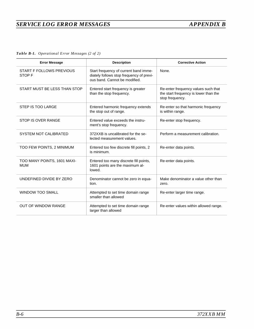
SERVICE LOG ERROR MESSAGES APPENDIX B
B-6 372XXB MM
Error Message Description Corrective Action
START F FOLLOWS PREVIOUSSTOP F
Start frequency of current band imme-diately follows stop frequency of previ-ous band. Cannot be modified.
None.
START MUST BE LESS THAN STOP Entered start frequency is greaterthan the stop frequency.
Re-enter frequency values such thatthe start frequency is lower than thestop frequency.
STEP IS TOO LARGE Entered harmonic frequency extendsthe stop out of range.
Re-enter so that harmonic frequencyis within range.
STOP IS OVER RANGE Entered value exceeds the instru-ment’s stop frequency.
Re-enter stop frequency.
SYSTEM NOT CALIBRATED 372XXB is uncalibrated for the se-lected measurement values.
Perform a measurement calibration.
TOO FEW POINTS, 2 MINIMUM Entered too few discrete fill points, 2is minimum.
Re-enter data points.
TOO MANY POINTS, 1601 MAXI-MUM
Entered too many discrete fill points,1601 points are the maximum al-lowed.
Re-enter data points.
UNDEFINED DIVIDE BY ZERO Denominator cannot be zero in equa-tion.
Make denominator a value other thanzero.
WINDOW TOO SMALL Attempted to set time domain rangesmaller than allowed
Re-enter larger time range.
OUT OF WINDOW RANGE Attempted to set time domain rangelarger than allowed
Re-enter values within allowed range.
Table B-1. Operational Error Messages (2 of 2)

APPENDIX B SERVICE LOG ERROR MESSAGES
372XXB MM B-7
Error Message Description Corrective Action
7140 GENERAL FLOPPY DRIVEFAIL
Invalid disk media or format. Use 1.44 MB diskette and/or format inthe 372XXB.
7142 FLOPPY DISK READ ERROR Read error when accessing disk file. Use 1.44 MB diskette and/or format inthe 372XXB.
7143: FLOPPY DISK WRITE ERROR Error in writing to disk file. Use 1.44 MB diskette and/or format inthe 372XXB.
7147 FLOPPY DISK UNAVAILABLE Floppy disk is not available. Install floppy diskette and/or checkfloppy disk drive.
7170: GENERAL HARD DISK FAIL General error in accessing hard disk. Retry and if still fails, reformat thehard disk drive and/or check floppydisk drive.
7172: HARD DISK READ ERROR Read error when accessing disk file. Retry and if still fails, reformat thehard disk drive and/or check floppydisk drive.
7173: HARD DISK WRITE ERROR Error in writing to disk file. Retry and if still fails, reformat thehard disk drive and/or check floppydisk drive.
7177: HARD DISK UNAVAILABLE Hard disk is not available. Install hard disk drive and/or checkoperation of hard disk.
8140: GENERAL DISK BUFFER ER-ROR
Out of RAM. Press the System State, Default Pro-gram key, and retry. This will reset the372XXB to the factory default state.
FILE NOT FOUND Disk file not found. None.
FLOPPY DISK HAS NO ROOM FORFILE
Floppy diskette is full. Delete files or install new diskette.
FLOPPY DISK NOT READY Floppy disk is not ready (or not in-stalled.).
Install diskette in floppy drive.
FLOPPY DISK WRITE PROTECTED Write protect tab in place on floppydiskette.
Remove write-protect tab.
HARD DISK HAS NO ROOM FORFILE, DELETE EXISTING FILES(S)TO CREATE SPACE
Hard disk is full. Delete unneeded files.
Table B-2. Disk-Related-Error Messages (1 of 1)

SERVICE LOG ERROR MESSAGES APPENDIX B
B-8 372XXB MM
Error Message Description
These errors are entered in the Service Log and output as part of the response of OGE/OGL commands for GPIB com-mands. The list is subdivided into the type of GPIB error: 7204..., 7205..., 7206..., and 7207.
7204 GPIB COMMAND ERROR DESCRIPTIONS
Faulty program mnemonic syn-tax
Generated when the program mnemonic found was not one of the currently definedprogram mnemonics for the 372XXB.
Faulty suffix mnemonic syntax Generated when the suffix mnemonic found was not one of the currently defined suffixmnemonics for the 372XXB.
Faulty mnemonic syntax Generated when the mnemonic found was not one of the currently defined program orsuffix mnemonics for the 372XXB.
Missing Program Message Sep-arator
Generated when the required semicolon preceding the next program mnemonic wasnot found.
Expected NRf data Generated when a mnemonic is used that requires a trailing NRf numeric data ele-ment. The data element was either missing or the first character of the data elementwas not one of the acceptable NRf characters.
NRf mantissa too long The maximum allowable number of characters in the NRf numeric element mantissa is255.
Exponent magnitude too large The maximum allowable exponent magnitude in an NRf element is +/— 32000.
Faulty NRf syntax Can be any number of syntactical errors such as more than one decimal point, inclu-sion of a decimal point in the exponent field, an invalid character imbedded in the nu-meric or no exponent value following the ‘E’.
Expected String Program Data Generated when a mnemonic is used that requires a trailing string data element. Thedate element was either missing or no open quote character was found.
Missing close quote character Generated when a mnemonic is used that requires a trailing string data element. Theopen quote character was found, but the close quote character was not.
Expected Arbitrary Block data Generated when a mnemonic is used that requires a trailing arbitrary block data ele-ment and the trailing element was not an arbitrary block data element. Or in somecases, the arbitrary block was empty.
Faulty Arbitrary Block Generated when a defined length arbitrary block data element is terminated early withan EOI or an indefinite length arbitrary block data element is not properly terminated.
Missing Program Data Separator Two data elements of a program mnemonic that requires multiple program data ele-ments, are not properly separated from each other by a comma.
Table B-3. GPIB-Related Error Messages (1 of 8)

APPENDIX B SERVICE LOG ERROR MESSAGES
372XXB MM B-9
Error Message Description
GET received during PM recep-tion
Generated when the GPIB Command ‘Group Execute Trigger’ is received during thereception of a program message but before its proper termination with the end mes-sage. The partial program message up to but not including the ‘Group Execute Trig-ger’ will be executed. Execution of the Group Execute Trigger and any subsequentprogram message elements received before the end message will be skipped.
7205 GPIB EXECUTION ERROR DESCRIPTIONS
Not permitted in a DDT com-mand sequence
When executing a defined device trigger command sequence, a forbidden commandwas detected.
Too much Arbitrary Block data The arbitrary block supplied contained more data than was necessary for the currentlydefined 372XXB state. This can occur when graph types, start/stop frequencies ordata points are changed.
Insufficient Arbitrary Block data The arbitrary block supplied did not have enough data for the currently defined372XXB state. This can occur when graph types, start/stop frequencies or data pointsare changed.
Invalid parameter for currentgraph type
An attempt was made to program a non-existent parameter for the current graph type.For instance, a Smith chart does not have a reference or reference line position (mne-monics OFF and REF).
Parameter out of range An attempt was made to program an out of integer range value for a parameter. Thiserror is detected by the GPIB MANAGER when converting and rounding to the appro-priate integral size (signed/unsigned char/short or long).
Parameter value not permitted A parameter value was not found in the list of permissible values for that parameter.
CW marker sweep not permittedin time domain
The mnemonics M1C, M2C, M3C, M4C, M5C and M6C are forbidden in time domain.
Parameter unavailable in fre-quency domain
The mnemonic ODV and OTV are forbidden in frequency domain.
Port 2 Test Attenuator (OPT 6)not installed
The mnemonic TA2 is forbidden when the attenuator is not installed.
Time Domain (OPT 2) not in-stalled
An attempt was made to use one of the time domain mnemonics when the option isnot installed.
Return to Local not permitted inLocal Lockout
The mnemonic RTL failed due to being in the Local Lockout mode.
Calibration does not exist An attempt was made to turn on flat power correction or vector error correction whenthe corresponding calibration does not exist.
Cal term not available An attempt was made to get a calibration term which does not exist for the current cal-ibration type.
Table B-3. GPIB-Related Error Messages (2 of 8)

SERVICE LOG ERROR MESSAGES APPENDIX B
B-10 372XXB MM
Error Message Description
Invalid cal term for calibrationtype
An attempt was made to program a calibration term which does not exist for the cur-rent calibration type.
Front panel setup not valid An attempt was made to get a front panel setup that did not contain a correct/validstate.
Normalization data not valid An attempt was made to reference normalization data when there was no normaliza-tion data currently stored.
Command sequence too long An attempt was made to define a device trigger command sequence which had morethan 255 characters.
Unable to display menu An attempt was made to display a menu which could not be displayed for the current372XXB state.
String too long An attempt was made to enter a string for the following mnemonics which exceededthe specified maximum length.
LTD, LID, LMS and LNM - maximum length is 15 characters.
LOC - maximum length is 79 characters.
Must specify a calibration typefirst
In order to perform a calibration, the calibration type must be specified by the use ofone of the Cxx mnemonics (i.e. C12, C8T, etc.) PRIOR to the issuance of the mne-monics CWC, TDC or BEG.
Parameter value unchanged An attempt was made to change a start/stop frequency or number of data points to avalue outside of the current calibrated range with correction turned on.
Parameter change not permitted An attempt was made to perform an illegal state change or action based on the cur-rent 372XXB state. This includes attempting to store an undefined band definition. Orcertain changes from the calibration state or the calibration define state when definingdiscrete frequencies.
Parameter value out of rangeParameter out of hardwarerange
An attempt was made to set a parameter to a value outside of the permissible rangeof values for the parameter.
Standard cal method not validfor waveguide
In a waveguide type of calibration, the standard (OSL) cal method is forbidden.
Out of calibrated range An attempt was made to change a parameter not permitted to be changed with correc-tion on.
Start must be must be less thanstop
An attempt was made to set a new start frequency, distance or time greater than orequal to the current stop frequency, distance or time. Or to set a new stop frequency,distance or time less than or equal to the current start frequency, distance or time.
Tune mode requires a 12 termcalibration
Perform a 12 term calibration prior to turning on tune mode.
Table B-3. GPIB-Related Error Messages (3 of 8)
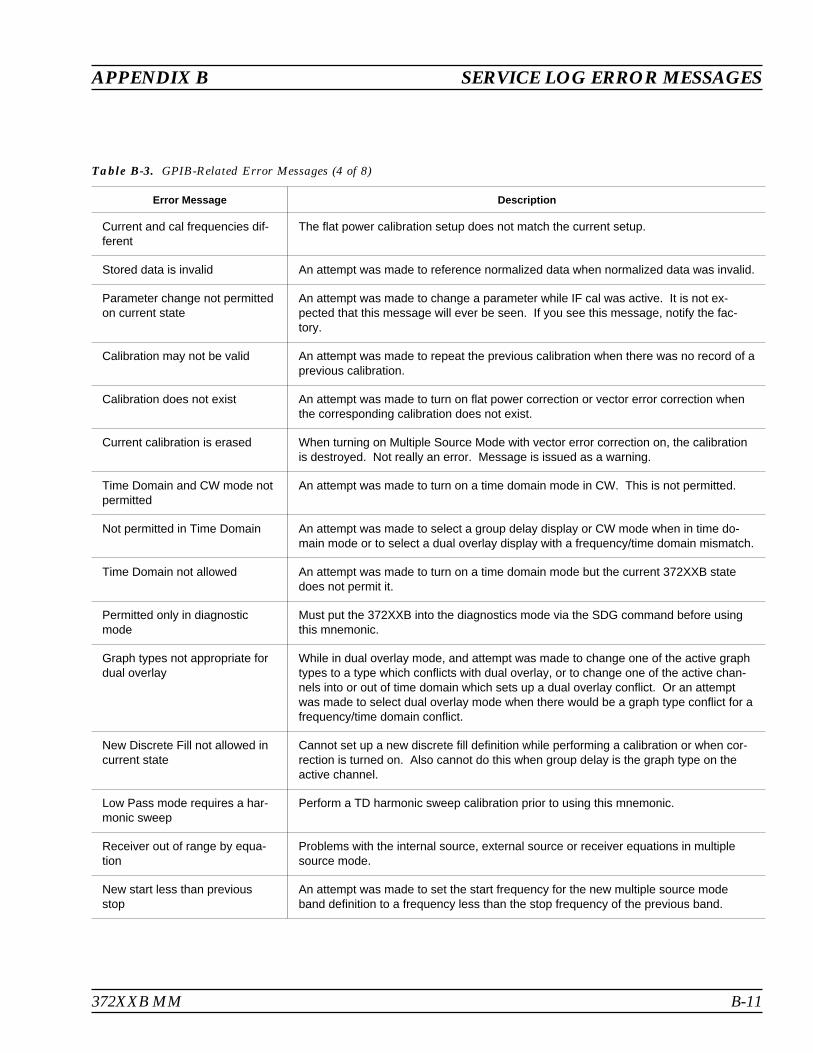
APPENDIX B SERVICE LOG ERROR MESSAGES
372XXB MM B-11
Error Message Description
Current and cal frequencies dif-ferent
The flat power calibration setup does not match the current setup.
Stored data is invalid An attempt was made to reference normalized data when normalized data was invalid.
Parameter change not permittedon current state
An attempt was made to change a parameter while IF cal was active. It is not ex-pected that this message will ever be seen. If you see this message, notify the fac-tory.
Calibration may not be valid An attempt was made to repeat the previous calibration when there was no record of aprevious calibration.
Calibration does not exist An attempt was made to turn on flat power correction or vector error correction whenthe corresponding calibration does not exist.
Current calibration is erased When turning on Multiple Source Mode with vector error correction on, the calibrationis destroyed. Not really an error. Message is issued as a warning.
Time Domain and CW mode notpermitted
An attempt was made to turn on a time domain mode in CW. This is not permitted.
Not permitted in Time Domain An attempt was made to select a group delay display or CW mode when in time do-main mode or to select a dual overlay display with a frequency/time domain mismatch.
Time Domain not allowed An attempt was made to turn on a time domain mode but the current 372XXB statedoes not permit it.
Permitted only in diagnosticmode
Must put the 372XXB into the diagnostics mode via the SDG command before usingthis mnemonic.
Graph types not appropriate fordual overlay
While in dual overlay mode, and attempt was made to change one of the active graphtypes to a type which conflicts with dual overlay, or to change one of the active chan-nels into or out of time domain which sets up a dual overlay conflict. Or an attemptwas made to select dual overlay mode when there would be a graph type conflict for afrequency/time domain conflict.
New Discrete Fill not allowed incurrent state
Cannot set up a new discrete fill definition while performing a calibration or when cor-rection is turned on. Also cannot do this when group delay is the graph type on theactive channel.
Low Pass mode requires a har-monic sweep
Perform a TD harmonic sweep calibration prior to using this mnemonic.
Receiver out of range by equa-tion
Problems with the internal source, external source or receiver equations in multiplesource mode.
New start less than previousstop
An attempt was made to set the start frequency for the new multiple source modeband definition to a frequency less than the stop frequency of the previous band.
Table B-3. GPIB-Related Error Messages (4 of 8)

SERVICE LOG ERROR MESSAGES APPENDIX B
B-12 372XXB MM
Error Message Description
Bad filename The supplied filename was bad. The filename can have 8 characters maximum. Noextensions. The filename must start with and alpha type character (A thru Z). Afterthat the allowable characters are alpha, numeric (0 thru 9) and underscore (_).
Conflict with rotary knob You should not be using the rotary knob and the GPIB at the same time.
Too many data points for exter-nal source
A 6700B series external source can handle 501 data points.A 68000 series external source can handle 999 data points.
Recalled setup corruptedHardware mismatch in recalledsetupSoftware mismatch in recalledsetup
These are problems with the recalled setup.
Too many data points for Dis-crete Fill
The maximum number of data points in discrete fill is 1601.
Not enough data points for Dis-crete Fill
The minimum number or data points in discrete fill is 2.
Discrete Fill end frequency out ofrange
The number of points for discrete fill puts the end frequency out of range.
Step is too large When setting up a time domain harmonic sweep, cannot get 2 data points becausethe start frequency is too high for the approximate stop frequency. In a group delaydisplay, the delay aperture percent of sweep is less than one step size.
Range too small An attempt was made to set a distance or time span value too small. This can also bedone via inappropriate values for start and stop.
Start or stop out of range An attempt was made to set a distance or time start or stop value out of range. Thiscan also be done via inappropriate values for center and span.
No bands defined An attempt was made to turn on multiple source mode with no band definitions.
Out of frequencies for new banddefinitionSource out of range by equationExternal source out of range byequation
The current set of multiple source mode bands use up all the frequency range of the372XXB. Therefore, no more bands can be defined.
File is read only An attempt was made to write to a write protected file.
File not found An attempt was made to access a non-existent file.
Floppy drive not ready An attempt was made to access the floppy drive with no floppy disk installed.
Floppy disk fullHard disk full
An attempt was made to write to a floppy disk or the hard disk when no space was lefton the disk.
Table B-3. GPIB-Related Error Messages (5 of 8)

APPENDIX B SERVICE LOG ERROR MESSAGES
372XXB MM B-13
Error Message Description
Floppy disk write protected An attempt was made to write to a write protected floppy disk.
Recalled setup or data file cor-rupt
An attempt to recall a setup from internal memory, the GPIB or disk failed due to soft-ware revision or hardware mismatch or checksum error.
New frequency list not allowed incurrent state
Cannot set up a new discrete fill definition while performing a calibration or when cor-rection is turned on. Also, cannot do this when group delay is the graph type on theactive channel.
State change not permitted An attempt was made to perform an illegal state change or action based on the cur-rent instrument state. This includes attempting to store (1) an undefined band defini-tion, (2) certain changes from the calibration state, or (3) the cal define state whendefining discrete frequencies.
Faulty label or file name The label or file name associated with the current mnemonic is faulty.
Illegal characters in filename The first character in a filename must be an alpha type. The remaining characters canbe alpha, numeric, or underscores. An extension is not permitted.
Filename too long The maximum ledngth for filenames is 8 characters. An extension is not permitted.
Floppy disk read errorFloppy disk write errorHard disk read errorHard disk write error
Read or write error(s) occurred while attempting to access the indicated disk.
Floppy disk not foundHard disk not foundGeneral disk buffer errorGeneral floppy drive failureFloppy disk init failureGeneral hard disk failureHard disk control failureHard disk init failureUnknown disk error
Other error messages which suggest that the indicated drive is in need of service.
7205 GPIB QUERY ERROR DESCRIPTIONS
No Response data available Generated if the controller attempts to read response data from the 372XXB and noneis available.
No Response data after PMcompletion
This is the same as the ‘no response data available’ case above except that a pro-gram message was currently being parsed and executed when the controller at-tempted to read data. Detection of this error was deferred until the parser/executionblock was finished with the current program message and it was observed that no re-sponse data was generated.
Table B-3. GPIB-Related Error Messages (6 of 8)

SERVICE LOG ERROR MESSAGES APPENDIX B
B-14 372XXB MM
Error Message Description
Response after Indefinite Re-sponse discarded
This error is generated when the 372XXB’s output queue has already received an Ar-bitrary ASCII response data element and an attempt is made to place another re-sponse data element of any kind into the queue. The new response data element isdiscarded.
Interrupted - Response data dis-carded
This error is detected when the output queue contains unread response data and thecontroller sends a new program message. The response data is discarded.
Unterminated - Partial PM will beexecuted
This error is detected when the 372XXB’s input queue is currently receiving a programmessage but has not yet received the end message, and the controller attempts toread response data from the 372XXB. The partial program message in the inputqueue is executed as if it were properly terminated.
Deadlock - Response data dis-carded
This error is detected when both of the 372XXB’s input and output queues are full andthe controller attempts to send another data byte. In order to prevent bus deadlock,the contents of the output queue are discarded.
7205 GPIB DEVICE DEPENDENT ERROR DESCRIPTIONS
Q_SEND failure in [a procedurename]
An unsuccessful attempt was made to send a message to a task.
The procedure name is the place in the software where the error was detected.
Q_RECEIVE failure in [a proce-dure name]
A failure was detected while waiting for the reception of a message from a task.
The procedure name is the place in the software where the error was detected.
Unable to allocate memory in [aprocedure name]
An attempt was made to allocate some temporary memory in order to accomplish atask directed in the program message.
The procedure name is the place in the software where the error was detected.
Unable to release memory in [aprocedure name]
An attempt was made to return some temporary memory within a task and the returnfailed for some reason.
The procedure name is the place in the software where the error was detected.
Unable to get service/error log An unsuccessful attempt was made to get a copy of the service or error log.
Unable to get calibration term An unsuccessful attempt was made to get a calibration term.
Unable to get raw or correcteddata
An unsuccessful attempt was made to get raw or corrected data.
Unable to get final data An unsuccessful attempt was made to get final data.
Unable to get setup or data An unsuccessful attempt was made to get the frequency list from the database.
Unable to get setup An unsuccessful attempt was made to get a front panel setup.
Table B-3. GPIB-Related Error Messages (7 of 8)

APPENDIX B SERVICE LOG ERROR MESSAGES
372XXB MM B-15
Error Message Description
Unable to store setup An unsuccessful attempt was made to save a front panel setup.
Unable to get frequency list An unsuccessful attempt was made to get setup, trace, or tabular datat from the data-base.
Unable to store label An unsuccessful attempt was made to store a label in the database.
Calibration step failure An error occurred while waiting for completion of a data collection sequence in calibra-tion.
Table B-3. GPIB-Related Error Messages (8 of 8)

SERVICE LOG ERROR MESSAGES APPENDIX B
B-16 372XXB MM
0000 INFORMATIONAL MESSAGE
0000 SELF TEST INFO MESSAGE
0094 PRNT INTERFACE TEST PASSED
0095 PRNT INTERFACE TEST FAILED
0096 GPIB INTERFACE TEST PASSED
0097 GPIB INTERFACE TEST FAILED
0098 SELF TEST PASSED
0099 SELF TEST FAILED
0111 LO1 COMM FAIL
0112 LO1 PRE TUNE DAC FAIL
0113 LO1 PHS LCK IND FAIL
0114 PHS LCK ERR VOL OUT OF TOL
0115 LO1 LCK TIME FAIL
0211 LO2 COMM FAIL
0212 LO2 MAIN PREST DAC FAIL
0213 LO2 OFFS PREST DAC FAIL
0214 MAIN PHS LCK ERR VOL FAIL
0215 OFFST PHS LCK ERR VOL FAIL
0216 DDS PHS LCK ERR VOL FAIL
0217 MAIN PHS LCK IND FAIL
0218 OFFST PHS LCK IND FAIL
0219 DDS PHS LCK IND FAIL
0220 LO2 LCK TIME FAIL
0221 LO2 SRC TRACKING FAIL
0311 TA IF COMM FAIL
0312 TA IF 10V REF FAIL
0313 TA IF LEVEL STATUS FAIL
0314 TA PHS CONTROL FAIL
0411 REF IF COMM FAIL
0412 REF IF 10V REF FAIL
0413 REF IF LEV STATUS FAIL
0414 REF PHS CONTROL FAIL
0500 A TO D CONVERSION FAIL
0511 A TO D COMM FAIL
0512 A TO D 8 BIT D TO A FAIL
0513 A TO D 12 BIT A TO D FAIL
0514 A TO D STEERING DAC FAIL
0515 A TO D CONV ACCURACY FAIL
0516 A TO D SAMPL HOLD FAIL
0517 IF SYNC FAIL
0518 PWR SUPPLY SYNC FAIL
0519 A TO D EXT ANAL OUTP FAIL
0520 PWR SUPPLY +5V FAIL
0521 PWR SUPPLY +9V FAIL
0522 PWR SUPPLY +12V FAIL
0524 PWR SUPPLY +18V FAIL
0525 PWR SUPPLY -18V FAIL
0526 PWR SUPPLY +27V FAIL
0527 PWR SUPPLY -27V FAIL
0611 TB IF COMM FAIL
0612 TB IF 10V REF FAIL
0613 TB IF LEVEL STATUS FAIL
0614 TB PHS CONTROL FAIL
0711 LO3 COMM FAIL
0712 LO3 REF OSC FAIL
0713 LO3 48.4 LCK IND FAIL
0714 LO3 48.4 LCK ERR VOL FAIL
0715 LO3 CAL REF PHS FAIL
0811 SL SIG SEP COMM FAIL
0812 DAC ADJUSTMENT FAIL
0813 TRANSFER SWITCH CNTRL FAIL
0814 SRC LCK POL CONTROL FAIL
0815 DIRECT MODE ATTEN FAIL
0911 A9 VME BUS INTERFACE FAIL
0912 BBRAM CHECK FAIL
0913 SRAM CHECK FAIL
Table B-4. Service Log Error Messages (1 of 3)

APPENDIX B SERVICE LOG ERROR MESSAGES
372XXB MM B-17
0914 SCSI DEVICE FAIL
0915 MCCHIP FAIL
0915 MCCHIP TIMER 1 FAIL
0916 MCCHIP TIMER 2 FAIL
0917 MCCHIP TIMER 3 FAIL
0918 MCCHIP TIMER 4 FAIL
0919 CLOCK NOT RUNNING
1311 A13 VME BUS INTERFACE FAIL
1312 EXT KEYBD CNTRL FAIL
1313 FLOPPY DISK CNTRL FAIL
1411 A14 VME BUS INTERFACE FAIL
1511 A15 VME BUS INTERFACE FAIL
1512 VRAM CHECK FAIL
1611 HARD DISK CONTROL FAIL
1811 AUXILLARY IO FAIL
1912 FRONT PANEL CNTRL FAIL
1913 ROTARY KNOB FAIL
2111 SRC COMM FAIL
2112 SRC FTUNE DAC FAIL
2113 SRC STATE MACHINE DAC FAIL
2114 SRC FM CAL FAIL
2115 SRC F TUNE PATH BND1 FAIL
2116 SRC F TUNE PATH BND2 FAIL
2117 SRC F TUNE PATH BND3 FAIL
2118 SRC F TUNE PATH BND4 FAIL
2119 SRC F TUNE PATH BND5 FAIL
2120 SRC F TUNE PATH BND6 FAIL
2121 SRC F TUNE PATH BND7 FAIL
2122 SRC F TUNE PATH BND8 FAIL
2123 SRC F TUNE PATH BND9 FAIL
2124 SRC F TUNE PATH BND10 FAIL
2125 SRC PWR LEVEL DAC FAIL
2126 SRC DETECTOR ZERO CAL FAIL
2127 SRC ALC CAL BND1 FAIL
2128 SRC ALC CAL BND2 FAIL
2129 SRC ALC CAL BND3 FAIL
2130 SRC ALC CAL BND4 FAIL
2131 SRC ALC CAL BND5 FAIL
2132 SRC ALC CAL BND6 FAIL
2133 SRC ALC CAL BND7 FAIL
2134 SRC ALC CAL BND8 FAIL
2135 SRC ALC CAL BND9 FAIL
2136 SRC ALC CAL BND10 FAIL
2137 SRC A1 FM PATH TUNE FAIL
2138 SRC A2 FM PATH TUNE FAIL
4100 LO1 CAL FAIL
4200 LO2 CAL FAIL
4301 SRC FREQ CAL MEAS UNSTABLE
4302 SRC FREQ FM MAIN CAL FAIL
4303 SRC FREQ FM SENS CAL FAIL
4304 SRC FREQ CAL VERIFY FAIL
4401 SRC ALC LOG AMP CAL FAIL
4402 SRC ALC CAL VERIFY FAIL
4500 IF CAL FAIL
4600 GAIN RANGING ERROR
4700 STATE MACHINE FAIL
5110 RF PWR UNLEVELED
5210 REF A CHAN RF OVERLOAD
5220 REF B CHAN RF OVERLOAD
5230 TA CHAN RF OVERLOAD
5240 TB CHAN RF OVERLOAD
6001 - 6128 PHASE LOCK FAILURE
7100 FILE MARKED READ ONLY
7140 GENERAL FLOPPY DRIVE FAIL
7142 FLOPPY DISK READ ERROR
7143 FLOPPY DISK WRITE ERROR
Table B-4. Service Log Error Messages (2 of 3)

SERVICE LOG ERROR MESSAGES APPENDIX B
B-18 372XXB MM
7146 FLOPPY DISK CHANGED
7147 FLOPPY DISK UNAVAILABLE
7169 FLOPPY INIT FAIL
7170 GENERAL HARD DISK FAIL
7172 HARD DISK READ ERROR
7173 HARD DISK WRITE ERROR
7177 HARD DISK UNAVAILABLE
7199 HARD DISK INIT FAIL
7200 IEEE 488.2 GPIB BUS ERROR
7201 ABORTED MESSAGES
7202 NOTHING TO SAY
7203 NO LISTENER ON BUS
7204 GPIB COMMAND ERROR
7205 GPIB EXECUTION ERROR
7206 GPIB DEVICE SPECIFIC ERROR
7207 GPIB QUERY ERROR
7210 DEDICATED GPIB BUS ERROR
7220 PLOTTER NOT RESPONDING
7221 PLOTTER NOT READY
7222 PLOTTER OUT OF PAPER
7223 PLOTTER PEN UP
7230 POWER METER NOT RESPONDING
7240 FRQ COUNTER NOT RESPONDING
7250 EXT SOURCE NOT RESPONDING
7310 PRINTER NOT RESPONDING
7311 PRINTER NOT READY
7312 PRINTER OUT OF PAPER
7320 AUX I/O PORT ERROR
7330 SERIAL PORT ERROR
7340 ETHERNET PORT ERROR
7350 EXT TRIG RATE TOO FAST
7410 EXT KYBD ERROR
8100 PWR FAIL
8110 GENERAL VME BUS FAIL
8120 GENERAL MEMORY FAIL
8121 NON-VOLATILE MEMORY FAIL
8130 PROCESSING FAIL
8140 GENERAL DISK BUFFER ERR
Table B-4. Service Log Error Messages (3 of 3)

Table of ContentsC-1 INTRODUCTION · · · · · · · · · · · · · · · · · · · · · · · · · C-3
C-2 PRECAUTIONS · · · · · · · · · · · · · · · · · · · · · · · · · C-3
C-3 REPAIR/ MAINTENANCE · · · · · · · · · · · · · · · · · · · · C-5
372XXB MM C-1
Appendix CConnector MaintenanceCheck Procedures


Appendix CConnector MaintenanceCheck Procedures
C-1 INTRODUCTION This appendix provides general, precautionary information and in-structions pertaining to precision connectors.
C-2 PRECAUTIONS The following paragraphs are precautionary notes relating to mainte-nance considerations for precision connectors
Pin Depth ProblemsBased on ANRITSU precision components returned for repair, destruc-tive pin depth of mating connectors is the major cause of failure in thefield. When a precision component is mated with a connector having adestructive pin depth, damage will likely occur to the precision compo-nent’s connector. A connector is considered to have destructive pindepth when the center pin is too long in respect to the connector’s ref-erence plane (Figure C-1).
Before mating an unknown or new device with your 372XXB Port con-nectors or calibration devices, always measure the pin depth of the de-vice’s connectors. Use a ANRITSU Pin Depth Gauge, or equivalent, forthese measurements (Figure C-2). Also, measure the connectorpin-depth of a device when intermittent or degraded performance issuspected.
Gauging sets for measuring the pin-depth of precision connectors areavailable from your nearest ANRITSU Service center, or from the fac-tory. Instructions for measuring connector pin-depth are included withthe gauging set(s).
372XXB MM C-3
REFERENCEPLANE
MALE
PINDEPTH
(INCHES)
REFERENCEPLANE
FEMALE
PINDEPTH
(INCHES)
Figure C-1.
01
2
3
45
1
2
3
4
21 1
2
Figure C-2. Pin Depth Gauge

Pin-Depth ToleranceThe center pin of a precision connector has a tolerances measured inmils (one mil = 1/1000 inch). The connectors of test devices may not beprecision types and they may not have the proper pin-depth. Theseconnectors should be measured before mating to ensure suitability.
When gauging pin depth, if the connector being measured indicatesout of tolerance in the “+” region of the gauge (Table C-1), the centerpin is too long. Mating under this condition will likely damage themating connector. On the other hand, if the test device connector indi-cates out of tolerance in the “–” region, the center pin is too short.While this will not cause any damage, it will result in a poor connec-tion and a consequent degradation in performance.
Avoid Over TorquingConnectors
Over-torquing connectors is destructive; it may damage the connectorcenter pin. Finger-tight is usually sufficient, especially on Type N con-nectors. Should it be necessary to use a wrench to tighten SMA orWSMA connectors, use a torque wrench that breaks at 8 inch-pounds.As a general rule, never use pliers to tighten connectors.
Teflon TuningWashers
The center conductor on many precision connectors contains a smallteflon tuning washer located near the point of mating (interface). Thiswasher compensates for minor impedance discontinuities at the inter-face. The washer’s location is critical to the connector’s performance.Do not disturb it.
Avoid MechanicalShock
Precision connectors are designed to withstand years of normal benchhandling. Do not drop or otherwise treat them roughly. They are labo-ratory-quality devices, and like other such devices, they require care-ful handling.
C-4 372XXB MM
PRECAUTIONS APPENDIX C
Port/Conn. Type
Pin Depth(MILS)
GaugeReading
GP7C- +0.000–0.003
Same AsPin Depth
N Male 207
–0.000+0.004
207
+0.000–0.004
N Female 207
–0.004+0.000
Same AsPin Depth
3.5 mm Male, Female –0.000+0.002
K Male, Female +0.0000–0.0035
V Female +0.000to –0.001
Table C-1. Connector Pin-Depth Tolerance

Keep ConnectorsClean
The precise geometry that makes a precision connector’s high perfor-mance possible can be disturbed by dirt and other contamination ad-hering to connector interfaces. When not in use, keep the connectorscovered.
VisualInspection
Precision connectors should be inspected periodically. Check for thefollowing:
� Bent or broken center pin� Damaged threads� Other bent or damaged connector parts� Dirt or foreign material in connector cavity.
C-3 REPAIR/MAINTENANCE
ANRITSU recommends that no maintenance other than cleaning beattempted by the customer. Any device with a suspected defective con-nector should be returned to ANRITSU for repair and/or service whenneeded.
372XXB MM C-5/C-6
APPENDIX C REPAIR/ MAINTENANCE

Appendix DPerformance Specifications
SYSTEM PERFORMANCEFrequency Range:RF Models:37217B 22.5 MHz to 8.6 GHzMicrowave Models37225B 40 MHz to 13.5 GHz37247B 40 MHz to 20 GHz37269B 40 MHz to 40 GHz37297B 40 MHz to 65 GHzDynamic Range:The following table gives dynamic range in two manners.“Receiver Dynamic Range” is defined as the ratio of themaximum signal level at Port 2 for 0.1 dB compression tothe noise floor at Port 2. “System Dynamic Range” is de-fined as the ratio of the power incident on Port 2 in athrough line connection to the noise floor at Port 2 (forwardmeasurements only). In preparing the table, 10 Hz IFbandwidth and 512 averages were used in calibration andmeasurement.
High Level Noise (typical)<0.03 dB and <0.4° peak-to-peak variation in a 1 kHz IFbandwidth up to 20 GHz. <0.08 dB and <0.5°
peak-to-peak variation up to 40 GHz.Measurement Throughput:Measurement times are based on a single 40 MHz to 20GHz sweep with 10 kHz IF bandwidth (no averages) aftera full 12-term calibration. Sweep times include retrace andbandswitch times.
Measurement Time (ms) vs. Data Points (typical):
CalibrationType
Data Points
3 51 101 401 1601
1 Port (3 Term) 60 250 330 960 3300
Full 2 Port 60 270 400 1000 3600
Measurement Time vs. Sweep Mode for 101 DataPoints (typical):
Sweep Mode Time (ms)
Linear 350
List 350
CW 230
Measurement Time vs. IF Bandwidth for 101 DataPoints (typical):
IF Bandwidth Time (ms)
10 kHz 350
1 kHz 530
100 Hz 1900
10 Hz 14000
Measurement Time vs. Span for 101 Data Points (typi-cal):
Frequency Span Time (ms)
40 MHz to 40 GHz 500
20 GHz to 40 GHz 400
10 GHz to 11 GHz 250
TEST PORT CHARACTERISTICSThe specifications in the following table apply when theproper Model 34U Universal Test Port Adapters are con-nected, with or without phase equal insertables, to the testset ports and calibrated with the appropriate Anritsu orother designated calibration kit at 23°C ±3°C using theOSL calibration method with a sliding load to achieve
372XXB OM D-1
Model Freq(GHz)
Max Sig-nal IntoPort 2(dBm)
NoiseFloor(dBm)
ReceiverDynamicRange
Port 1Power(dBm)
Sys.Dy-
namicRange
37217B0.0225 +3 –95 98 0 95
2 +3 –98 101 0 98
8.6 +3 –98 101 0 98
37225B0.04 +20 –70 90 0 70
2 +3 –98 101 0 98
13.5 +3 –98 101 0 98
37247B0.04 +20 –70 90 0 70
2 +3 –98 101 0 98
20 +3 –96 99 0 96
37269B
0.04 +20 –70 90 0 55
2 +3 –98 101 0 83
20 +3 –95 98 –5 80
40 +3 –93 96 –15 78
37297B
0.04 +20 –77 97 +10 70
2 +3 –105 108 +10 98
20 +3 –97 100 –2 90
40 +3 –95 98 –7 78
50 +3 –87 90 –2 80
60 +3 –77 80 –2 70

12-Term error correction (A 90 minute warm-up time is rec-ommended.)
MEASUREMENT CAPABILITIESNumber of Channels: Four independent measurementchannels.Parameters: S11, S21, S22, S12, or user-defined com-binations of a1, a2, b1, and b2. All measurements aremade without the need to manually reverse the test device.Measurement Frequency Range: Frequency range ofmeasurement can be narrowed within the calibration rangewithout recalibration. CW mode permits single frequencymeasurements, also without recalibration. In addition, thesystem accepts N discrete frequency points where2£N£1601.Domains: Frequency Domain, CW Draw, and optionalHigh Speed Time (Distance) Domain.Formats: Log Magnitude, Phase, Log Magnitude andPhase, Smith Chart (impedance), Smith Chart (Admit-tance), Linear Polar, Log Polar, Group Delay, Linear Mag-nitude, Linear Magnitude and Phase, Real, Imaginary, Realand Imaginary, SWR, Power.Data Points: 1601 maximum. Data points can beswitched to a value of 801, 401, 201, 101, or 51 pointswithout recalibration (if 1601 points were used in the cali-bration). In addition, the system accepts an arbitrary set ofN discrete data points where: 2£N£1601. CW mode per-mits selection of a single data point without recalibration.
Reference Delay: Can be entered in time or in distance(when the dielectric constant is entered). Automatic refer-ence delay feature adds the correct electrical length com-pensation at the push of a button. Software compensationfor the electrical length difference between reference andtest is always accurate and stable since measurement fre-quencies are always synthesized. In addition, the systemcompensates reference phase delay for dispersive trans-mission media, such as waveguide and microstrip.Markers: Six independent markers can be used to readout measurement data. In delta-reference marker mode,any one marker can be selected as the reference for theother five. Markers can be directed automatically to theminimum or maximum of a data trace.Enhanced Markers: Marker search for a level or band-width, displaying an active marker for each channel, anddiscrete or continuous (interpolated) markers.Marker Sweep: Sweeps upward in frequency betweenany two markers. Recalibration is not required during themarker sweep.Limit Lines: Either single or segmented limit lines canbe displayed. Two limit lines are available for each trace.Single Limit Readouts: Interpolation algorithm deter-mines the exact intersection frequencies of test data andlimit lines.
D-2 372XXB MM
PERFORMANCE SPECIFICATIONS APPENDIX D
ConnectorFrequency
(GHz)Directivity
(dB)Source Match
(dB)Load Match
(dB)
ReflectionFrequency
Tracking (dB)
TransmissionFrequency Track-
ing (dB)
Isolation(dB)
GPC-7 0.0225 >52 >44 >52 ±0.003 ±0.004 >105
2.0 >52 >44 >52 ±0.003 ±0.004 >115
18 >52 >42 >52 ±0.004 ±0.012 >112
GPC-7 LRLCalibration
2.0 >60 >60 >60 ±0.001 ±0.001 >115
18 >60 >60 >60 ±0.001 ±0.001 >112
N-Type 0.0225 >46 >36 >46 ±0.004 ±0.004 >105
2.0 >44 >36 >44 ±0.004 ±0.004 >115
18 >40 >32 >40 ±0.005 ±0.012 >112
3.5 mm 0.0225 >44 >40 >44 ±0.005 ±0.030 >105
2.0 >44 >40 >44 ±0.005 ±0.030 >115
20 >44 >38 >44 ±0.006 ±0.050 >110
26.5 >44 >34 >44 ±0.006 ±0.070 >102
K 0.0225 >42 >40 >42 ±0.005 ±0.030 >105
2.0 >42 >40 >42 ±0.005 ±0.050 >115
20 >42 >34 >42 ±0.006 ±0.070 >110
40 >38 >34 >38 ±0.006 ±0.080 >100
V 0.04 >70 >36 >40 ±0.050 ±0.030 >105
2.0 >40 >36 >40 ±0.050 ±0.050 >115
20 >40 >36 >40 ±0.060 ±0.070 >110
40 >36 >32 >36 ±0.060 ±0.080 >100
50 >34 >30 >34 ±0.080 ±0.100 >90
65 >34 >28 >34 ±0.100 ±0.120 >80

Segmented Limit Lines: A total of 20 segments (10 up-per and 10 lower) can be generated per data trace. Com-plete segmented traces can be offset in both frequencyand amplitude.Test Limits: Both single and segmented limits can beused for PASS/FAIL testing. The active channel’s PASS orFAIL status is indicated on CRT after each sweep. In addi-tion, PASS/FAIL status is output through the rear panel I/Oconnector as selectable TTL levels (PASS=0V, FAIL=+5V,or PASS=+5V, FAIL=0V).Tune Mode: Tune Mode optimizes sweep speed in tun-ing applications by updating forward S-parameters morefrequently than reverse ones. This mode allows the user toselect the ratio of forward sweeps to reverse sweeps aftera full 12-term calibration. The ratio of forward sweeps toreverse sweeps can be set anywhere between 1:1 to10,000:1.
DISPLAY CAPABILITIESDisplay Channels: Four, each of which can display anyS-parameter or user defined parameter in any format withup to two traces per channel for a maximum of eight tracessimultaneously. A single channel, two channels (1 and 3,or 2 and 4), or all four channels can be displayed simulta-neously. Channels 1 and 3, or channels 2 and 4 can beoverlaid.Monitor: Color, 7.5-inch diagonal, VGA display or8.4-inch diagonal LCD. The default color configuration isas follows: graticules are displayed in green, measurementdata in red, markers and limits in blue, and overlaid tracedata in yellow. Trace data stored in memory are displayedin green.Trace Color: The color of display traces, memory, text,markers and limit lines are all user definable.Trace Overlay: Displays two data traces on the activechannel’s graticule simultaneously. The overlaid trace isdisplayed in yellow and the primary trace is displayed inred.Trace Memory: A separate memory for each channelcan be used to store measurement data for later display orsubtraction, addition, multiplication or division with currentmeasurement data.Scale Resolution (minimum):
Log Magnitude: 0.001 dB/divLinear Magnitude: 1 pUPhase: 0.01o
Group Delay: 0.001 psTime: 0.001 msDistance: 0.1 mmSWR: 1 pUPower: 0.05 dBAutoscale: Automatically sets Resolution and Offset tofully display measurement data.
Reference Position: Can be set at any graticule line.
Annotation: Type of measurement, vertical and horizon-tal scale resolution, start/stop or center/span frequencies,and reference position.Blank Frequency Information: Blanking function re-moves all references to displayed frequencies on the CRT.Frequency blanking can only be restored through a systemreset or GPIB command.
MEASUREMENT ENHANCEMENTData Averaging: Averaging of 1 to 4096 averages canbe selected. Averaging can be toggled on/off with frontpanel button. A front panel button turns data averagingon/off, and a front panel LED indicates when averaging isactive.Video IF Bandwidth: Front panel button selects fourlevels of video IF bandwidth. MAXIMUM (10 kHz), NOR-MAL (1 kHz), REDUCED (100 Hz) and MINIMUM (10 Hz).Trace Smoothing: Functions similarly to Data Averagingbut computes an average over a percentage range of thedata trace. The percentage of trace to be smoothed canbe selected from 0 to 20% of trace. Front panel buttonturns smoothing on/off, and front panel LED indicateswhen smoothing is active.
SOURCE CONTROLFrequency Resolution: 1 kHz (1 Hz standard on RFunits and optional on Microwave units - Option 10A)Source Power Level: The source power (dBm) may beset from the 372XXB front panel menu or via GPIB.Refer to Level Control Range table on next page.Power Accuracy: ±0.5 dB at 2 GHz at default power.Level Test Port Power: The power, at all sweep fre-quencies, is leveled to within
±1.5dB (0.0225–13.5 GHz)±2.0dB (13.5–20 GHz)±3.0 dB (20–40 GHz)
Power Meter Correction: The 372XXB offers auser-selectable feature that corrects for test port powervariations and slope (on Port 1) using an external Hewle-tt-Packard 437B or Anritsu ML8403 power meter. Powermeter correction is available at a user-selectable powerlevel, if it is within the power adjustment range of the inter-nal source. Once the test port power has been flattened,its level may be changed within the remaining power ad-justment range of the signal source.Set-On Receiver Mode: The 372XXB can be configuredto measure the relative harmonic level of test devices withSet-On Receiver Mode capability. The 372XXB’s uniquephase locking scheme allows it to operate as a tuned re-ceiver by locking all of its local oscillators to its internalcrystal reference oscillator. Set-On Receiver Mode capabil-ity significantly increases the versatility of the 372XXB VNAin applications that check for harmonics, intermodulationproducts, and signals of known frequency.
372XXB MM D-3
APPENDIX D PERFORMANCE SPECIFICATIONS

Dual Source Control Capability: Dual Source Controlcapability allows a user to independently control the fre-quencies of two sources and the receiver without the needfor anexternal controller. The frequency ranges and outputpowers of the two sources may be specified. A frequencysweep may be comprised of up to five separate bands,each with independent source and receiver settings, forconvenient testing of frequency translation devices such asmixers. Up to five sub-bands may be tested in one sweep.This feature enables users to easily test mixers, up/downconverters, multipliers, and other frequency conversion de-vices.
Source 1: The 372XXB internal source.Source #2: Any of ANRITSU’s family of 68000B,68100B, 68200B, 68300B, 69XXXA, or 6700Bsynthesizers.Sweep Type: Linear, CW, Marker, or N-Discrete pointsweep.
POWER RANGE
ModelRated Power
(dbm)Minimum Power
(dBm)Resolution (dB)
37217B 0 –20 0.05
37225B 0 –20 0.05
37247B 0 –20 0.05
37269B –15 –27 0.05
37297B –7 –19 0.05
LEVEL CONTROL RANGE
37217B 37225B 37247B 37269B 37297B
Above ResetPower*
+10 dB +10 dB +10 dB +20 dB +20 dB
Below ResetPower
-20 dB -20 dB -20 dB -12 dB -20 dB <47 GHz-12 dB ³47 GHz
*Source power above the reset level is allowed but not guaranteed,especially over the full frequency range.
D-4 372XXB MM
PERFORMANCE SPECIFICATIONS APPENDIX D
22.5 MH 8.6 GH
MODEL 37211A AND 37217A PORT 1 POWER
LOG MAG 5DB/DIVREF 0DBM
AVAILABLEPOWER
TYPICAL
LOG MAG 5DB/DIVREF 0DBM
40 MH 20 GH
TYPICAL
AVAILABLEPOWER
MODEL 37225A AND 37247A PORT 1 POWER
Model 37217B Port 1 Power
Model 37225B and 37247B Port 1 Power
LOG MAG REF -15DBM 5DB/DIV
40 MH 40 GH
MODEL 37269A PORT 1 POWER
AVAILABLEPOWER
TYPICAL
Model 37269B Port 1 Power
40 MH 65 GH
MODEL 37297B AND 37397A PORT 1 POWER
LOG MAG 5DB/DIVREF 0DBM
AVAILABLEPOWER
TYPICAL
Model 37277B/37297B Port 1 Power
-7 dBm

POWER FLATNESS
Frequency Range (GHz) Flatness (dB)
0.0225 to 13.5 1.5
13.5 to 20 2.0
20 to 40 3.0
40 to 65 5.0
SOURCE PURITY(Specifications apply for all models at maximum ratedpower.)Harmonics & Harmonic Related:35 dBc (37217B, 37225B, 37247B, 37269B)15 dBc (37297B)Nonharmonics: 35 dBc (standard)Phase Noise: >60 dBc/Hz at 10 kHz offset and 20 GHzcenter frequency
SOURCE FREQUENCY ACCURACYStandard Time Base:
Aging: <1 x 10⁻⁶/yearStability: <1 x 10⁻⁶ over +15oC to +50oC range
High Stability Time Base (Option 10):Aging: <1 x 10⁻⁹/dayStability: <5 x 10⁻⁹ over 0oC to +55oC range
GROUP DELAY CHARACTERISTICSGroup Delay is measured by computing the phase changein degrees across a frequency step by applying the for-mula:
� g
dd f
� � 11
360/
�
Aperture: Defined as the frequency span over which thephase change is computed at a given frequency point. Theaperture can be changed without recalibration. The mini-mum aperture is the frequency range divided by the num-ber of points in calibration and can be increased to 20% ofthe frequency range without recalibration. The frequencywidth of the aperture and the percent of the frequencyrange are displayed automatically.Range: The maximum delay range is limited to measur-ing no more than +180° of phase change within the aper-ture set by the number of frequency points. A frequencystep size of 100 kHz corresponds to 10 ms.Measurement Repeatability (sweep to sweep): Forcontinuous measurement of a through connection, RSSfluctuations due to phase and FM noise are:
141 2 2. [ ( ) ( ) ]PhaseNoise in deg Residual FM Noise in Hzg� �� 0 5
360
.
( )Aperture in Hz
Accuracy:
Error inError in Phase deg
Aperture Freq Eg g� �� � �\ ( )
[ .360
rror Hz
Aperture Hz
( ) ]
( )
VECTOR ERROR CORRECTIONThere are five methods of calibration:
1) Open-Short-Load (OSL). This calibration methoduses short circuits, open circuits, and terminations (fixedor sliding)2) Offset-Short (waveguide): This calibration methoduses short circuits and terminations.3) LRL/LRM: The Line-Ref lect-Line (LRL) orLine-Reflect-Match (LRM) calibration uses transmissionlines and a reflective device or termination (LRM).4) TRM: The Thru-Reflect-Match calibration uses shortcircuits and fixed termination.5) AutoCal: The VNA will serially drive an externalAutoCal module to perform a 2-port OSLT calibration.AutoCal is a single two port calibration module withbuilt-in, switched, and characterized OSLT standards.AutoCal provides quick, reliable, and accurate calibra-tions that exceed the performance of a standard broad-band load OSLT calibration.
There are four vector error correction models available:1) Full 12-Term2) One Path/Two Port3) Frequency Response (Transmission/Reflection)4) Reflection Only Full 12-term can always be used, ifdesired, since all 372XXB-series models automatically re-verse the test signal. Front-panel display indicates thetype of calibration stored in memory. Front-panel buttonselects whether calibration is to be applied, and an LEDlights when error correction is being applied.
There are four vector error correction models available:1) Full 12-Term2) One Path/Two Port3) Frequency Response (Transmission/Reflection)4) Reflection Only
Full 12-term can always be used, if desired, since all372XXB-series models automatically reverse the test sig-nal. Front-panel display indicates the type of calibrationstored in memory. Front-panel button selects whether cali-bration is to be applied, and an LED lights when error cor-rection is being applied.Calibration Sequence: Prompts the user to connect theappropriate calibration standard to Port 1 and/or Port 2.Calibration standards may be measured simultaneously orone at a time.Calibration Standards: For coaxial calibrations the userselects SMA, GPC-3.5, GPC-7, Type N, 2.4 mm, TNC, K,or V Connector from a calibration menu. Use of fixed orsliding loads can be selected for each connector type.
372XXB MM D-5
APPENDIX D PERFORMANCE SPECIFICATIONS

User defined calibration standards allow for entry of opencapacitance, load and short inductances, load impedance,and reflection standard offset lengths.Reference Impedance: Modify the reference impedanceof the measurement to other than 50 ohms (but not 0).LRL/LRM Calibration Capability: The LRL calibrationtechnique uses the characteristic impedance of a length oftransmission line as the calibration standard. A full LRLcalibration consists merely of two transmission line mea-surements, a high reflection measurement, and an isolationmeasurement. The LRM calibration technique is a variationof the LRL technique that utilizes a precision terminationrather that a second length of transmission line. A third op-tional standard, either Line or Match, may be measured inorder to extend the frequency range of the calibration. Thisextended calibration is achieved by mathematically concat-enating either two LRL, two LRM, or one LRL and oneLRM calibration(s). Using these techniques, full 12-term er-ror correction can be performed on the 372XXB VNA.Adapter Removal Calibration: Built-in Adapter Removalapplication software accurately characterizes and “re-moves” any adapter used during calibration what will notbe used for subsequent device measurements. This tech-nique allows for accurate measurement of non-insertabledevices.Dispersion Compensation: Selectable as Coaxial(non-dispersive), Waveguide, or Microstrip (dispersive).Reference Plane: Selectable as Middle of line 1 or Endsof line 1.Corrected Impedance: Determined by Calibration Stan-dards.
HARD COPYPrinter: Menu selects full screen, graphical, tabulardata, S2P or Text output, and printer type. The number ofdata points of tabular data can be selected as well as dataat markers only. Compatible with the 2225C InkJet, HPQuietJet, HP 310/320/340 DeskJet, HP 500 Deskjet, HP560C DeskJet (b/w only), HP LaserJet II, III, & IV Series,and some Epson compatible printers with Parallel (Centr-onics) interfaces.GPIB Plotters: The 37XXX VNA is compatible with HPModels 7440A, 7470A, 7475A, and 7550A (in standardmode) and Tektronix Model HC100 plotters. Menu selectsplotting of full or user-selected portions of graphical data.Plotter is connected to the dedicated GPIB bus.Performance: After selecting the Start Print button, frontpanel operation and measurement capability is restored tothe user within 2 seconds.
STORAGEInternal Memory: Ten front panel states (setup/calibra-tion) can be stored and recalled from non-volatile memorylocations. The current front panel setup is automatically
stored in non-volatile memory at instrument power-down.When power is applied, the instrument returns to its lastfront panel setup.Internal Hard Disk Drive: Used to store and recall mea-surement and calibration data and front-panel setups. Allfiles are MS-DOS compatable. File names can be 1 to 8characters long, and must begin with a character, not anumber. Extensions are automatically assigned.External SCSI Interface: Option 4 deletes the internalhard disk drive, and adds a SCSI Interface connector tothe rear panel for connecting a SCSI-2 formatted hard diskdrive.Internal Floppy Disk Drive: A 3.5-inch diskette drivewith 1.44 Mbytes formatted capacity is used to load mea-surement programs and to store and recall measurementand calibration data and front panel setups. All files areMS-DOS compatable. File names can be 1 to 8 charac-ters long, and must begin with a character, not a number.Extensions are automatically assigned.Measurement Data: 102.8 kbytes per 1601 pointS-parameter data file.Calibration Data: 187.3 kbytes per 1601 pointS-parameter data file (12-term cal plus setup).Trace Memory File: 12.8 kbytes per 1601 point chan-nel.
GPIBGPIB INTERFACES - 2 PORTSSystem GPIB (IEEE-488.2): Connects to an externalcontroller for use in remote programming of the networkanalyzer. Address can be set from the front panel and canrange from 1 to 30.Interface Function Codes: SH1, AH1, T6, TE0, L4,LE0, SR1, RL1, PP1, DT1, DC0, C0.Dedicated GPIB: Connects to external peripherals fornetwork analyzer controlled operations (e.g. GPIB plotters,frequency counters, frequency synthesizers, and powermeters).GPIB Data Transfer Formats: ASCII, 32-bit floatingpoint, or 64-bit floating point. 32-bit and 64-bit floating pointdata can be transferred with LSB or MSB first.
GPIB DATA COLLECTION SUMMARYThis section summarizes typical data collection times forautomated measurements using the 37XXX IEEE 488.2GPIB bus. Throughput measurements for both tables weremade as follows: start the timer, trigger a sweep, wait for afull sweep, transfer data across the GPIB and stop thetimer. Data throughput times are shown separately formeasurements made without calibration and with fulltwo-port, 12-term calibration.Data Transfer Speed (with or without cal): 62kbytes/second
D-6 372XXB MM
PERFORMANCE SPECIFICATIONS APPENDIX D

Measurement conditions: 40 MHz to 20 GHz sweep,single channel, log magnitude display, 10 kHz IF band-width, and output final data.Throughput Times (ms) without Correction (typical)
Data Format 3 Points* 101 Points 401 Points 1601 Points
32 Bit 230 830 2100 7000
64 Bit 230 850 2700 7100
ASCII 235 1000 2400 8000
Throughput Times (ms) with Correction (typical)
Data Format 3 Points* 101 Points 401 Points 1601 Points
32 Bit 340 1200 2600 7800
64 Bit 350 1200 2700 8300
ASCII 350 1280 3000 9300
GENERAL372XXB Front Panel Connectors and Controls:
Keyboard Input: An IBM-AT compatible keyboard canbe connected to the front panel for navigating throughfront panel menus and disk directories, annotation of datafiles and display labels, printing displays and pausing in-strument sweeps.Test Ports: Universal/K, male, connectors are standardon all models except for 37297B, which uses VConnectors. For other configurations check Option 7. Foradditional configurations check Test Port Converters.
37200B Rear Panel Connectors and Controls:PRINTER OUT: Centronics interface for an externalprinter.VGA OUT: Provides VGA output of 372XXB video dis-play.10 MHz REF IN: Connects to external reference fre-quency standard, 10 MHz, +5 to –5 dBm, 50 ohms, BNCfemale.10 MHz REF OUT: Connects to internal reference fre-quency standard, 10 MHz, 0 dBm, 50 ohms, BNC female.EXT ANALOG OUT: –10V to +10V with 5 mV resolu-tion, varying in proportion to user-selected data (e.g., fre-quency, amplitude). BNC female.EXT ANALOG IN: ±50 volt input for displaying externalsignals on the CRT in Diagnostics mode. BNC female.
LINE SELECTION: Power supply automat ical lysenses 100V, 120V, 220V or 240V lines.EXTERNAL TRIGGER: External triggering for 372XXBmeasurement, ±1V trigger. 10 kohm input impedance.BNC female.REFERENCE EXTENSION: Provides access to thea1 sampler (optional); K or V Connector, female.EXTERNAL SCSI: Provides SCSI-2 connector for con-nection of an external SCSI hard disk drive (Opt. 4).EXTERNAL I/O: 25-pin DSUB connector.EXTERNAL SCSI: Provides SCSI-2 connector for con-nection of an external SCSI hard disk drive (Opt. 4).
SERIAL: Provides control for AutoCal module.LIMITS PASS/FAIL: Selectable TTL levels(Pass=0V, Fail=+5V or Pass=+5V, Fail=0V. Addi-tionally, 0 volts (all displayed channels pass) or +5V(any one of 4 displayed channels fail) output pass/failstatus (1 line).EXTERNAL TRIGGER: External tr iggering for372XXB measurement, ±1V trigger. 10 kohm input im-pedance. BNC female.EXT ANALOG OUT: –10V to +10V with 5 mV reso-lution, varying in proportion to user-selected data (e.g.,frequency, amplitude). BNC female.
Power Requirements: 85-240V, 48-63 Hz, 540 VA maxi-mumDimensions: 267H x 432W x 585D mm (10.5H x 17W x23D in.)Weight: 34 kg (75 lb) - Maximum amount specified for2-man lift requirement.
ENVIRONMENTALStorage Temperature Range: –40°C to +75°COperating Temperature Range: –0°C to +50°CRelative Humidity: 5% to 95% at +40°CEMI: Meets the emissions and immunity requirements ofEN55011/1991 Class A/CISPR-11 Class AEN 50082-1/1993
IEC 801-2/1984 (4 kV CD, 8kV AD)IEC 1000-4-3/1995 (3 V/m, 80-1000 MHz)IEC 801-4/1988 (500V SL, 1000V PL)IEC 1000-4-5/1995 (2 kV L-E, 1kV L-L)
HIGH SPEED TIME (DISTANCE) DOMAINMEASUREMENT CAPABILITY (OPTION 2A)
Option 2A, High Speed Time (Distance) Domain softwareallows the conversion of reflection or transmission mea-surements from the frequency domain to the time domain.Measured S-parameter data is converted to the time do-main by application of a Fast Fourier Transform (FFT) us-ing the Chirp Z-Transform technique. Prior to conversionany one of several selectable windowing functions may beapplied. Once the data is converted to the time domain, agating function may be applied to select the data of inter-est. The processed data may then be displayed in the timedomain with display start and stop times selected by theuser or in the distance domain with display start and stopdistance selected by the user. The data may also be con-verted back to the frequency domain with a time gate toview the frequency response of the gated data.Lowpass Mode: This mode displays a response equiva-lent to the classic TDR (Time Domain Reflectometer) re-sponse of the device under test. Lowpass response maybe displayed in either the impulse or step mode. This typeof processing requires a sweep over a harmonic series offrequencies and an extrapolated or user-entered DC value.
372XXB MM D-7
APPENDIX D PERFORMANCE SPECIFICATIONS

D-8 372XXB MM
PERFORMANCE SPECIFICATIONS APPENDIX D
Bandpass Mode: This mode displays a response equiv-alent to the time response of the device under test to aband limited impulse. This type of processing may be usedwith any arbitrary frequency sweep range, limited only bythe test set range or device under test response.Phasor Impulse Mode: This mode displays a responsesimilar to the Lowpass impulse response, using data takenover an arbitrary (band limited) sweep range. Detailed in-formation, similar to that contained in the lowpass impulseresponse may be used to identify the nature of impedancediscontinuities in the device under test. Now, with PhasorImpulse, it is possible to characterize complex impedanceson band-limited devices.Windowing: Any one of four window functions may beapplied to the initial frequency data, to counteract the ef-fects of processing data with a finite bandwidth. These win-dows provide a range of tradeoffs of main lobe width ver-sus sidelobe level (ringing).The general type of function used is the Blackman-Harriswindow with the number of terms being varied from one tofour. Typical performance follows:
Types of Window(Number of Terms)
First Side LobeRelative to Peak
Impulse Width1
Rectangular (1) –13 dB 1.2W
Nominal-Hamming (2) –43 dB 1.8W
Low Side Lobe,Blackman-Harris (3)
–67 dB 2.1W
Minimum Side Lobe,Blackman-Harris (4)
–92 dB 2.7W
1 W(Bin Width) = 1/2Df sweep widthExample: When Df = 40 MHz to 40 GHz, W = 12.5 ps
When Df = 40 MHz to 65 GHz, W = 7.7 ps
Gating: A selective gating function may be applied to thetime domain data to remove unwanted responses, either ina pass-band or reject-band (mask). This gating functionmay be chosen as the convolution of any of the above win-dow types with a rectangular gate of user defined positionand width. The gate may be specified by entering start andstop times or center and span. The gated data may be dis-played in the time domain, or converted back to the fre-quency domain.
Time Domain Display: Data processed to time domainmay be displayed as a function of time or as a function ofdistance, provided the dielectric constant of the transmis-sion media is entered correctly. In the case of dispersivemedia such as waveguide or microstrip, the true distanceto a discontinuity is displayed in the distance mode. Thetime display may be set to any arbitrary range by specify-ing either the start and stop times or the center time andspan. The unaliased (non-repeating) time range is given bythe formula:
UnaliasiedRange nsNumber of Frequency Data PointsFre
( ) �quency Sweep Range GHz( )
The resolution is given by the formula:
Main Lobe Width null null in nskW
Freq Sweep Range GHz( \ )
( )�
Where kW is two times the number of window terms(for example, four for a two-term window)For a 40 GHz sweep range with 1601 data points, theunaliased range is 40.025 nanoseconds.For a 65 GHz sweep with 1601 data points, the unaliasedrange is 24.646 nanoseconds.Frequency with Time Gate: Data that has been con-verted to time domain and selected by the application ofgating function may be converted back to the frequencydomain. This allows the display of the frequency responseof a single element contained in the device under test. Fre-quency response accuracy is a function of window andgate type, and gate width. For a full reflection, minimumgate and window accuracy is within 0.2 dB of the ungatedresponse.
MEASUREMENT UNCERTAINTYThe graphs on pages C-9 through C-11 give measurementaccuracy after 12-term vector error correction. The errorsare worst case contributions of residual directivity, load andsource match, frequency response, isolation, network ana-lyzer dynamic accuracy, and connector repeatability. Inpreparing the following graphs, 10 Hz IF bandwidth andaveraging of 512 points were used (measured at 23±3° C).Changes in the IF bandwidth or averaging can result invariations at low levels.
* Upgrades from RF to microwave models maintain 1 Hz frequency resolutioncabability

372XXB MM D-9
APPENDIX D PERFORMANCE SPECIFICATIONS
DEVICE S21 (DB)
TRANSMISSION MAGNITUDE UNCERTAINTY37X47A/B/3652/TRANSMISSION ONLY
10
1
.1
-70 -60 -50 -40 -30 -20 -10 0 10-80-90
40 MH
2 GH
20 GH
40 MH
2 GH
20 GH
TRANSMISSION PHASE UNCERTAINTY37X47A/B/3652/TRANSMISSION ONLY
00
10
1
.1
DEVICE S21 (DB)-90 -80 -70 -60 -50 -40 -30 -20 -10 0 10
Model 37247B (K Connectors)Transmission Measurements:
REFLECTION MAGNITUDE UNCERTAINTY37X47A/B/3652/REFLECTION ONLY
10
1
.1
-40 -35 -30 -25 -20 -15 -10 -5 0
40 MH
2 GH
20 GH
REFLECTION PHASE UNCERTAINTY37X47A/B/3652/REFLECTION ONLY
DEVICE S11 (DB)
100
10
1
-40 -35 -30 -25 -20 -15 -10 -5 0
40 MH
2 GH
20 GH
Model 37247B (K Connectors)Reflection Measurements:

D-10 372XXB MM
PERFORMANCE SPECIFICATIONS APPENDIX D
D E V IC E S 21 (D B )
T R A N S M IS S IO N M A G N IT U D E U N C E R T A IN T Y37X 69A /B /3652 /T R A N S M IS S IO N O N LY
10
1
.1
-70 -60 -50 -40 -30 -20 -10 0 1 0-80-90
40 M H
2 G H
20 G H
40 G H
T R A N S M IS S IO N P H A S E U N C E R T A IN T Y37X69A /B /3652 /T RANSMISSION O NLY
100
10
1
.1
D E V IC E S 21 (D B )
-90 -80 -70 -60 -50 -40 -30 -20 -10 0 1 0
40 M H
2 G H
20 G H
40 G H
Model 37269B (K Connectors)Transmission Measurements:
REFLECTION MAGNITUDE UNCERTAINTY37X69A/B/3652/REFLECTION ONLY
DEVICE S11 (DB)
10
1
.1
-40 -35 -30 -25 -20 -15 -10 -5 0
40 MH
2 GH
20 GH
40 GH
REFLECTION PHASE UNCERTAINTY37X17A/B/3650/REFLECTION ONLY
DEVICE S11 (DB)
100
10
1
-40 -35 -30 -25 -20 -15 -10 -5 0
40 MH
2 GH
20 GH
40 GH
Model 37269B (K Connectors)Reflection Measurements:

372XXB MM D-11
APPENDIX D PERFORMANCE SPECIFICATIONS
Model 37297B (V Connectors)Transmission Measurements:
R E LE C T IO N M A G N IT U D E U N C E R T A IN T Y37X 97A /B /3654B /R E LE C T IO N O N LY
D E V IC E S 11 (D B )
1 0
1
.1
-4 0 -3 5 -30 -25 -20 -15 -10 -5 0
40 M H Z
20 G H Z
40 G H Z
50 G H Z
65 G H Z
R E LE C T IO N P H A S E U N C E R T A IN T Y37X 97A /B /3654B /R E LE C T IO N O N LY
D E V IC E S 11 (D B )
1 0 0
1 0
1
-4 0 -3 5 -30 -25 -20 -15 -10 -5 0
40 M H Z
20 G H Z
40 G H Z
50 G H Z
65 G H Z
Model 37297B (V Connectors)Reflection Measurements:

SYSTEM OPTIONSOPTION 1, Rack Mounting: Rack mount kit containing aset of track slides (90 tilt capability), mounting ears, andfront panel handles to let the instrument be mounted in astandard 19-inch equipment rack.OPTION 1A, Rack Mounting: Rack mounting kit contain-ing a set of mounting ears and hardware to permanentlymount instrument in a standard 19-inch equipment rack.OPTION 2, High Speed Time (Distance) DomainMeasurement CapabilityOPTION 3, 1 Hz Frequency Resolution: DeletedOPTION 4, External SCSI-2 Hard Disk Drive Compatibil-ity: Provides SCSI-2 rear panel connector for connectionof an external SCSI HDD. Remove internal HDD.OPTION 7A/N/NF/S/K, Universal Test Port Configura-tion Replaces Universal/K Connector (standard) with:
7A - Universal/GPC-77N - Universal/N, male7NF - Universal/N, female7S - Universal/3.5 mm, male
OPTION 10A, High Stability Time Base: Replaces thestandard temperature compensated crystal oscillator (witha temperature stability of 1ppm over a 0 to 55 °Crange)with an ovenized crystal oscillator (aging stability of1 x 10-9/day and temperature stability 5 x 10⁻⁹ over 0 to 55°C range). Adds 1 Hz frequency resolution.OPTION 11, Reference Loop: Reference loop to the a1
sampler; K or V Connector, female.
UPGRADE OPTIONS*37200A Upgrade to a higher frequency 37200A.37200A Upgrade to an equivalent or higher frequency37300A.37200B Upgrade to a higher frequency 37200B.37200B Upgrade to an equivalent or higher frequency37300A.37300A Upgrade to a higher frequency 37300A.
Please call your Anritsu representatives for pricing and de-livery.
ON-SITE SUPPORTOption ES 31: 3 year on-site repair.Option ES 37: 3 year on-site verificationOption ES 38: 3 year on-site Mil-Std verificationOption ES 51: 5 year on-site repair.Extended Service Options Additional, two year and fouryear return to Anritsu service is available, as an option for372XXB systems and components. Prices and details areavailable from your Sales Representative or by contactingthe factory.
CALIBRATION KITSStandard3650 SMA/3.5 mm Calibration Kit
Option 1: Male and Female Sliding Terminations3651 GPC-7 Calibration Kit
Option 1: Sliding Terminations3652 K Connector Calibration Kit
Option 1: Male and Female Sliding Terminations3653 Type N Calibration Kit3654B Type V Calibration Kit; includes male & femalesliding terminations
Economy (8.6 GHz)3750 SMA Calibration Kit3751 GPC-7 Calibration Kit3753 Type N, 50 W, Calibration Kit3753-75 Type N, 75 W, Calibration Kit
VERIFICATION KITS3663 Type N Verifications Kit3666 3.5 mm Verifications Kit3667 GPC–7 Verifications Kit3668 K Connector Verifications Kit3669B V Connector Verifications Kit
SEMI-RIGID TEST PORT CABLES3670A50-1, DC to 18 GHz, GPC–7 connectors, 1 footlong, two required.3670A50-2, DC to 18 GHz, GPC–7 connectors, 2 feetlong.3670K50-1, DC to 40 GHz, K connectors, 1 foot long,male/female, two required.3670K50-2, DC to 40 GHz, K connectors, 2 feet long,male/female.3670V50-1, DC to 65 GHz, V connectors, 1 foot long,male/female, two required.3670V50-2, DC to 65 GHz, V connectors, 2 feet long,male/female.
FLEXIBLE TEST PORT CABLES3671A50-1 GPC-7 Flexible Cables, 25 in. (1 pair).3671A50-2 GPC-7 Flexible Cable, 38 in.3671S50-1 3.5mm Flexible Cables, 25 in. (1 pair),male/male.3671S50-2 3.5mm Flexible Cable, 38 in., male.3671K50-1 K Connector Flexible Cables, 25 in.(1 pair), male/male.3671K50-2 K Connector Flexible Cable, 38 in., male.
D-12 372XXB MM
PERFORMANCE SPECIFICATIONS APPENDIX D
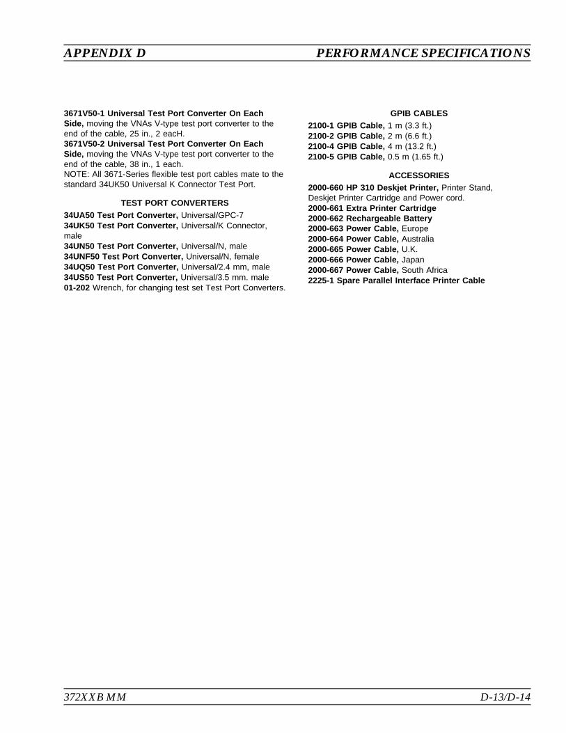
3671V50-1 Universal Test Port Converter On EachSide, moving the VNAs V-type test port converter to theend of the cable, 25 in., 2 eacH.3671V50-2 Universal Test Port Converter On EachSide, moving the VNAs V-type test port converter to theend of the cable, 38 in., 1 each.NOTE: All 3671-Series flexible test port cables mate to thestandard 34UK50 Universal K Connector Test Port.
TEST PORT CONVERTERS34UA50 Test Port Converter, Universal/GPC-734UK50 Test Port Converter, Universal/K Connector,male34UN50 Test Port Converter, Universal/N, male34UNF50 Test Port Converter, Universal/N, female34UQ50 Test Port Converter, Universal/2.4 mm, male34US50 Test Port Converter, Universal/3.5 mm. male01-202 Wrench, for changing test set Test Port Converters.
GPIB CABLES2100-1 GPIB Cable, 1 m (3.3 ft.)2100-2 GPIB Cable, 2 m (6.6 ft.)2100-4 GPIB Cable, 4 m (13.2 ft.)2100-5 GPIB Cable, 0.5 m (1.65 ft.)
ACCESSORIES2000-660 HP 310 Deskjet Printer, Printer Stand,Deskjet Printer Cartridge and Power cord.2000-661 Extra Printer Cartridge2000-662 Rechargeable Battery2000-663 Power Cable, Europe2000-664 Power Cable, Australia2000-665 Power Cable, U.K.2000-666 Power Cable, Japan2000-667 Power Cable, South Africa2225-1 Spare Parallel Interface Printer Cable
372XXB MM D-13/D-14
APPENDIX D PERFORMANCE SPECIFICATIONS

Appendix EPerformance VerificationSoftware User’s Guide
This appendix contains the Model 360X/37XXX Vector NetworkAnalyzer Performance VerificationSoftware User’s Guide. Thisuser’s guide provides technical data and procedures that canaid you in performing maintenance on the 372XXB.

SubjectIndex


Subject Index
Number37377A/37397A Source Lock Signal Path Diagram5- 2737377A/37397A Test Signal Path Diagram 5 - 26
AA21A2 ADJUSTMENT (37377A/37397A) 6 - 13,6 -14A8 ADJUSTMENT (37377A/37397A) 6 - 12Adjustments
A21A2 (37377A/37397A)· · · · · · · 6 - 13A8 (37377A/37397A) · · · · · · · · · 6 - 12Frequency Calibration · · · · · · · · 6 - 5Introduction to · · · · · · · · · · · · 6 - 3RF Power/ALC Calibration · · · · · · 6 - 8Source Lock Threshold · · · · · · · 6 - 11
ANRITSU Service Centers 1 - 9,2 - 4
BBBRAM Chip, Remove & Replace 8 - 6Boot-up Problems 5 - 7
CCalibration and Measurement Conditions 4 - 3Checking the Service Log 3 - 4Cleaning Connectors C - 5Connector Maintenance C - 3
Cleaning · · · · · · · · · · · · · · · · C - 5Mechanical Shock· · · · · · · · · · · C - 4Pin Depth Problems · · · · · · · · · C - 3Pin Depth Tolerances · · · · · · · · · C - 4Precautions · · · · · · · · · · · · · · C - 3Repair/Maintenance · · · · · · · · · C - 5Teflon Tuning Washer · · · · · · · · C - 4Torque · · · · · · · · · · · · · · · · · C - 4Visual Inspection · · · · · · · · · · · C - 5
Consummsable Parts 2 - 7CRT Display Test 3 - 6
DDiagnostic Menus A - 3Disk Related Error Messages B - 3
EElectro-static discharge procedures 1 - 9Error Code DE Lock Failure Troubleshooting 5 -14
Error Codes 5 - 10Error Messages B - 3
Disk Related · · · · · · · · · · · · · B - 3GPIB Related · · · · · · · · · · · · · B - 3Service Log · · · · · · · · · · · · · · B - 3
Exchange Assembly Program 2 - 3External Keyboard Interface Test 3 - 7
FFactory Repairable Non-Exchange Parts 2 - 8Failed Assembly Exchange Program 1 - 8Fan Assembly, Remove & Replace 8 - 21Field Service Kits 1 - 7Floppy Disk Drive, Remove & Replace 8 - 17Floppy Disk Problems 5 - 9Frequency Calibration Adjustment 6 - 5Front Panel Assembly, Remove & Replace 8 - 13Front Panel Test 3 - 7Functional Assembly Level Troubleshooting 1 - 5
GGPIB Interface Test 3 - 9GPIB Related Error Messages B - 3
HHard Disk Problems 5 - 8
IIdentification Number 1 - 3Internal Hardware Adjustments and Calibration 1- 5Isolation Procedures, Troubleshooting 5 - 19
LLCD, Remove & Replace 8 - 16
MMajor Assemblies Location Diagram (Bottom View)(Not 37377A or 37397A) 2 - 11Measurement Environment Considerations 4 - 6Measurement of Key System Performance Paramet4 - 6Measurement Technique 4 - 7Miscellaneous /Integrated Assemblies 2 - 7Module Exchange Program 2 - 3
372XXB MM Index-3

OOnline Manuals 1 - 3Operational Error Messages B - 3
PParts Ordering Information 2 - 4Performance Specifications 1 - 9,1 - 1Performance Verification 4 - 4Performance Verification Procedure 4 - 5Peripheral and Interfaces Tests 3 - 6Pin Depth
Problems · · · · · · · · · · · · · · · C - 3Tolerances · · · · · · · · · · · · · · · C - 4
Power Supply Module, Remove & Replace 8 - 21Precautions C - 3Preventive Service 1 - 6Printed Circuit Assemblies 2 - 5Printer Interface Test 3 - 7
RRear Panel Assembly, Remove & Replace 8 - 19Rear Panel PCB, Remove & Replace 8 - 22Recommended Test Equipment 1 - 9Related Manuals 1 - 4Removal and Replacement Procedures
LCD· · · · · · · · · · · · · · · · · · 8 - 16Remove and Replace Procedures 8 - 3
A12 VME Bus Terminator PCB · · · 8 - 12A13-A16 PCBs· · · · · · · · · · · · · 8 - 6A18 Rear Panel PCB· · · · · · · · · 8 - 22A1-A9 PCBs · · · · · · · · · · · · · · 8 - 6A9 PCB BBRAM Chip· · · · · · · · · 8 - 6A9 PCB SRAM Battery · · · · · · · 8 - 10Covers · · · · · · · · · · · · · · · · · 8 - 4Equipment Required · · · · · · · · · 8 - 3Fan Assembly · · · · · · · · · · · · 8 - 21Floppy Disk Drive · · · · · · · · · · 8 - 17Front Panel Assembly · · · · · · · · 8 - 13H/W (Hardware) Calibrations · · · · A - 5Installed Options · · · · · · · · · · · A - 4Operational · · · · · · · · · · · · · · B - 3Peripheral Tests · · · · · · · · · · · A - 4Power Supply Module · · · · · · · · 8 - 21Read Service Log · · · · · · · · · · · A - 3Rear Panel Assembly · · · · · · · · 8 - 19Signal Source Module Assemblies· · 8 - 29Start Self Test· · · · · · · · · · · · · A - 3Test Set Module Assemblies· · · · · 8 - 25Troubleshooting· · · · · · · · · · · · A - 4VGA Display Monitor · · · · · 8 - 14,8 - 16
Replacable Subassemblies and Parts 2 - 3RF Power/ALC Calibration Adjustment 6 - 8
SScope of Manual 1 - 3Screen Display Problems 5 - 10Self Test 3 - 5Service Centers 1 - 9service log B - 3Service Log 3 - 3,3 - 4,3 - 5,5 - 12Service Log Error Messages B - 3Service Logt 1 - 5Service Software 1 - 7Service Strategy 1 - 5Service Support Information 1 - 6Servicing Specially Modified Instruments 1 - 6Signal Path Tests 3 - 10Signal Source Module RF/Microwave Components2- 8Signal Source Modules, Remove & Replace 8 - 29Signal Source Problems 5 - 17Signal Source/Test Set Problems
Introduction to · · · · · · · · · · · · 5 - 18SOURCE LOCK THRESHOLD 6 - 11S-parameter 4 - 3Special Precautions 4 - 4Specifications, Performance 1 - 9,1 - 1SRAM Battery, Remove & Replace 8 - 10Standard Conditions 4 - 3Standard Options 1 - 4Static Sensitive Component Handling Procedure 1- 9System Description 1 - 4
A13 I/O Interface #1 PCB · · · · · · 7 - 15A14 I/O Interface #2 PCB · · · · · · 7 - 15A15 Graphic Processor PCB · · · · · 7 - 16A16 Hard Disk PCB · · · · · · · · · 7 - 16A17 System Motherboard · · · · · · 7 - 16A18 Rear Panel Interface PCB · · · 7 - 17A24 VME Bus Terminiator PCB · · 7 - 16A5 A/D Converter PCB · · · · · · · 7 - 12A7 PCB, LO3 · · · · · · · · · · · · · 7 - 12A8, Source Lock/Signal Separation & Con-trol · · · · · · · · · · · · · · · · · · 7 - 11A9 Main Processor PCB · · · · · · · 7 - 13Analog Subsystem Assemblies · · · · 7 - 7Digital Subsystem Assemblies · · · 7 - 13Front Panel Assembly · · · · · · · · 7 - 16Froppy Disk Drive · · · · · · · · · · 7 - 16IF Section · · · · · · · · · · · · · · 7 - 11
Index-4 372XXB MM
O TO S INDEX

Internal VGA Monitor · · · · · · · · 7 - 19Main Chassis Assemblies · · · · · · 7 - 16Overview· · · · · · · · · · · · · · · · 7 - 3Power Supply Module · · · · · · · · 7 - 18Rear Panel Assembly · · · · · · · · 7 - 17Receiver Module · · · · · · · · · · · 7 - 10Signal Source Module · · · · · · · · · 7 - 7Test Set Module · · · · · · · · · · · · 7 - 8
System Test Certification 1 - 6
TTechnical Support 1 - 7Test Fixtures/Aids 1 - 8Test Set Assembly RF/Microwave Components,37317A, 37325A, 37347A, 37369A 2 - 6Test Set Assembly RF/Microwave Components,37377A, 37397A 2 - 6Test Set Modules, Remove & Replace 8 - 25Torquing Connectors C - 4Troubleshooting
Association Information· · · · · · · · 5 - 3Boot-up Problems · · · · · · · · · · · 5 - 7Error Code Problems · · · · · · · · 5 - 10Floppy Disk Problems· · · · · · · · · 5 - 9Functional Level Assembly · · · · · · 1 - 5
Hard Disk Problems· · · · · · · · · · 5 - 8Introduction to · · · · · · · · · · · · 5 - 3Isolation Procedures · · · · · · · · · 5 - 19Line Source and Interface Checks · · 5 - 4Peripheral Interface · · · · · · · · · 5 - 21Power Supply Module Check · · · · · 5 - 6Power Supply Voltage Check · · · · · 5 - 4Power-up Problems · · · · · · · · · · 5 - 4Questionable Measurements · · · · 5 - 22Recommended Test Equipment· · · · 5 - 4Screen Display Problems · · · · · · 5 - 10Signal Source· · · · · · · · · · · · · 5 - 17Signal Source/Test Set· · · · · · · · 5 - 18
Tuning Washer C - 4Typical Reference Signal Values 5 - 25Typical SPDT Switch Voltages 5 - 25Typical Transfer Switch Voltages 5 - 25
VVerification Kits 1 - 8Verification Result Determination 4 - 5Verification Software 4 - 4Verifying Measurement Accuracy 4 - 4VGA Display Monitor, Remove & Replace 8 - 14Visual Inspection of Connectors C - 5VME Bus Terminator, Remove & Replace 8 - 12
372XXB MM Index-5/Index-6
INDEX T TO V