mm7150 data sheet - microchip technology
TRANSCRIPT

MM7150Motion Module
Product Features
• High Performance 32-bit Embedded Controller
• Cost effective solution
• Small form factor ideal for embedded applications
• Low power; 13.25mA in active mode
• System in deep sleep consumes 70µA
• Host interface via I2C
• 3.3-Volt I/O
• Package
- 17mm x 17mm, 16-pin module
Sensor Firmware
• Sensor fusion firmware features include:
- Self-contained 9-axis sensor fusion- Sensor data pass-through- Fast in-use background calibration of all sen-
sors and calibration monitor- Magnetic immunity: Enhanced magnetic dis-
tortion, detection and suppression- Gyroscope drift cancellation- Fully calibrated
• Easy to implement complete turnkey sensor fusion solution
• Sensor power management
• Sensors Supported
- Bosch BMC150 Geomagnetic Sensor/Accel-erometer
- Bosch BMG160 Gyroscope
Hardware Features
The hardware features in the MM7150 module includethe following:
• I2C Controller
- Supports I2C bus speeds to 400kHz
- Host Interface Supports Slave Operation
• Low Power Modes
Target Markets
• Internet of Things Applications
• Remote Controls, Gaming
• Fitness Monitoring
• Applications requiring data from an accelerome-ter, magnetometer and gyroscope
Temperature Ranges Available
• Industrial (-40°C to +85°C)
• Commercial (0°C to +70°C)
Description
The MM7150 Motion Module is a simple, cost-effectivesolution for integrating motion and positioning data intoa wide range of applications. The module contains theSSC7150 motion coprocessor with integrated 9-axissensor fusion as well as high performance MEMS tech-nology including a 3-axis accelerometer, gyroscopeand magnetometer. All components are integrated, cal-ibrated and available on the module for PCB mounting.
2015 - 2016 Microchip Technology Inc. DS00001888B-page 1

MM7150
TO OUR VALUED CUSTOMERS
It is our intention to provide our valued customers with the best documentation possible to ensure successful use ofyour Microchip products. To this end, we will continue to improve our publications to better suit your needs. Our pub-lications will be refined and enhanced as new volumes and updates are introduced.
If you have any questions or comments regarding this publication, please contact the Marketing CommunicationsDepartment via E-mail at [email protected]. We welcome your feedback.
Most Current Data SheetTo obtain the most up-to-date version of this data sheet, please register at our Worldwide Web site at:
http://www.microchip.com
You can determine the version of a data sheet by examining its literature number found on the bottom outside cornerof any page. The last character of the literature number is the version number, (e.g., DS30000000A is version A ofdocument DS30000000).
ErrataAn errata sheet, describing minor operational differences from the data sheet and recommended workarounds, mayexist for current devices. As device/documentation issues become known to us, we will publish an errata sheet. Theerrata will specify the revision of silicon and revision of document to which it applies.
To determine if an errata sheet exists for a particular device, please check with one of the following:
• Microchip’s Worldwide Web site; http://www.microchip.com
• Your local Microchip sales office (see last page)
When contacting a sales office, please specify which device, revision of silicon and data sheet (include -literaturenumber) you are using.
Customer Notification SystemRegister on our web site at www.microchip.com to receive the most current information on all of our products.
DS00001888B-page 2 2015 - 2016 Microchip Technology Inc.

2015 - 2016 Microchip Technology Inc. DS00001888B-page 3
MM7150
Table of Contents
1.0 MM7150 Pinout ............................................................................................................................................................................... 42.0 MM7150 Module ............................................................................................................................................................................. 73.0 MM7150 HID Functions .................................................................................................................................................................. 84.0 MM7150 Host Interface ................................................................................................................................................................. 125.0 MM7150 Firmware Update ........................................................................................................................................................... 136.0 MM7150 References ..................................................................................................................................................................... 147.0 MM7150 Performance .................................................................................................................................................................. 158.0 Electrical Characteristics ............................................................................................................................................................... 16Appendix A: Revision History .............................................................................................................................................................. 24The Microchip Web Site ...................................................................................................................................................................... 25Customer Change Notification Service ............................................................................................................................................... 25Customer Support ............................................................................................................................................................................... 25Product Identification System ............................................................................................................................................................. 26

MM7150
1.0 MM7150 PINOUT
The pinout of the MM7150 Motion Module is shown in the assembly drawing.
1.1 Assembly Drawing
The assembly drawing is shown in Figure 1-1.
FIGURE 1-1: ASSEMBLY DRAWING
DS00001888B-page 4 2015 - 2016 Microchip Technology Inc.

MM7150
1.2 Recommended Land Pattern
0.00mm
1
16
2.80mm
4.00mm
6.08mm
6.53mm
8.61mm
9.08mm
11.16mm
11.62mm
13.70mm
15.04mm
17.84mm
0.00
mm
2.80
mm
4.00
mm
6.08
mm
6.53
mm
8.61
mm
9.08
mm
11.1
6m
m
11.6
2m
m
13.7
0m
m
15.0
4m
m
17.8
4m
m
2015 - 2016 Microchip Technology Inc. DS00001888B-page 5

MM7150
1.3 Pin Descriptions
The pin descriptions are provided in Table 1-1.
TABLE 1-1: PIN DESCRIPTIONS
PinNumber
Name Type Description
1 HOST_TO_SH_WAKE I Used to wake Motion Module from a Sleep state. This signal must be driven high at least 11ms prior to sending any I2C traffic to the Motion Module. Active high input.
This pin should be connected to VDD through a 100KΩ resistor.
11 HOST_TO_SH_RESET I Reset input. Used to reset the host I2C interface.
This pin should be connected to VDD through a 100KΩ resistor.
4 HIDI2C_HOST_INT O Alert Interrupt signal from Motion Module to Host. Used to tell Host data from Motion Module is ready to be sent out. Active low output.
15 HIDI2C_HOST_CLK IOD I2C Controller Clock to Host Interface
16 HIDI2C_HOST_DAT IOD I2C Controller Data to Host Interface
10 NC1 - This pin should be left unconnected
2 NC2 - This pin should be left unconnected
9 NC3 - This pin should be left unconnected
12 NC4 - This pin should be left unconnected
13 NC5 - This pin should be left unconnected
14 NC6 - This pin should be left unconnected
3 NC7 - This pin should be left unconnected
5 NC8 - This pin should be left unconnected
6 NC9 - This pin should be left unconnected
7 VDD PWR VDD supply
8 VSS GND VDD associated ground
DS00001888B-page 6 2015 - 2016 Microchip Technology Inc.

2015 - 2016 Microchip Technology Inc. DS00001888B-page 7
MM7150
2.0 MM7150 MODULE
The MM7150 Motion Module provides 9-axis sensor fusion that includes a 3-axis accelerometer, a 3-axis gyroscopeand a 3-axis magnetometer. The module has an I2C interface to the host, and supports HID over I2C. The moduleincludes the Bosch BMC150 Geomagnetic Sensor/Accelerometer and Bosch BMG160 Gyroscope.
2.1 Module Block Diagram
The block diagram of the module is shown in Figure 2-1.
2.2 Module Features
The MM7150 Motion Module provides self-contained 9-axis sensor fusion. It supports fast in-use background calibrationof all sensors and calibration monitor. Magnetic immunity features provide enhanced magnetic distortion detection andsuppression. The module also provides gyroscope drift cancellation.
2.3 Calibration Requirements
User calibration is not required. The MM7150 Motion Module supports fast in-use background calibration of all sensorsand calibration monitor.
2.4 Other Information
To obtain the most recent and complete documentation for this module, including:
- User's Guide
- Board Description
- Board Schematics
- Source Code
- Application Examples
- Links to Web Seminars
Please refer to the web site: www.microchip.com/motion.
FIGURE 2-1: MM7150 MODULE BLOCK DIAGRAM
MicrochipSSC7150
Motion Coprocessor
Bosch BMG160
(Gyro)
Bosch BMC150
(A+M)
TPS22929Power Load
VSENSOR
HIDI2C_DEVICE_CLKHIDI2C_DEVICE_DAT
HIDI2C_HOST_DAT
HIDI2C_HOST_CLK
HIDI2C_HOST_INT
HOST_TO_SH_WAKE
D2_WAKE_UP
+3
.3V
GN
D
VDDVSS (x2)
AVSS
HOST_TO_SH_RESET
NC1NC2NC3NC4NC5NC6
MM7150
3.0 MM7150 HID FUNCTIONS
The MM7150 responds to the standard HID protocol for sensors when used over I2C, defined in References [1] and [2].The hierarchy of descriptors used in the HID protocol is as follows:
The following sections described the descriptors required for communicating with the MM7150:
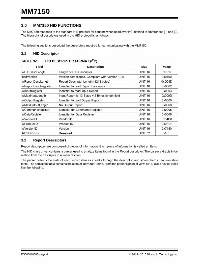
3.1 HID Descriptor
3.2 Report Descriptors
Report descriptors are composed of pieces of information. Each piece of information is called an Item.
The HID class driver contains a parser used to analyze items found in the Report descriptor. The parser extracts infor-mation from the descriptor in a linear fashion.
The parser collects the state of each known item as it walks through the descriptor, and stores them in an item statetable. The item state table contains the state of individual items. From the parser's point of view, a HID class device lookslike the following.
TABLE 3-1: HID DESCRIPTOR FORMAT (I2C)
Field Description Size Value
wHIDDescLength Length of HID Descriptor UINT 16 0x001E
bcdVersion Version compliance. Compliant with Version 1.00 UINT 16 0x0100
wReportDescLength Report Descriptor Length (3213 bytes) UINT 16 0x0C8D
wReportDescRegister Identifier to read Report Descriptor UINT 16 0x0002
wInputRegister Identifier to read Input Report UINT 16 0x0003
wMaxInputLength Input Report is 13 Bytes + 2 Bytes length field UINT 16 0x000D
wOutputRegistert Identifier to read Output Report UINT 16 0x0000
wMaxOutputLength No Output Report UINT 16 0x0000
wCommandRegister Identifier for Command Register UINT 16 0x0005
wDataRegister Identifier for Data Register UINT 16 0x0006
wVendorID Vendor ID UINT 16 0x04D8
wProductID Product ID UINT 16 0x0F01
wVersionID Version UINT 16 0x7150
RESERVED Reserved UINT 32 0x0
DS00001888B-page 8 2015 - 2016 Microchip Technology Inc.

MM7150
The Report descriptor is unlike other descriptors in that it is not simply a table of values. The length and content of aReport descriptor vary depending on the number of data fields required for the device’s report or reports. The Reportdescriptor is made up of items that provide information about the device.
The HID report for each sensor has two sections Feature Report and Input Report. The feature report for all the sen-sors is same. The following sections describe the Feature Report and all Input Reports returned by the Motion Module.
2015 - 2016 Microchip Technology Inc. DS00001888B-page 9
MM7150
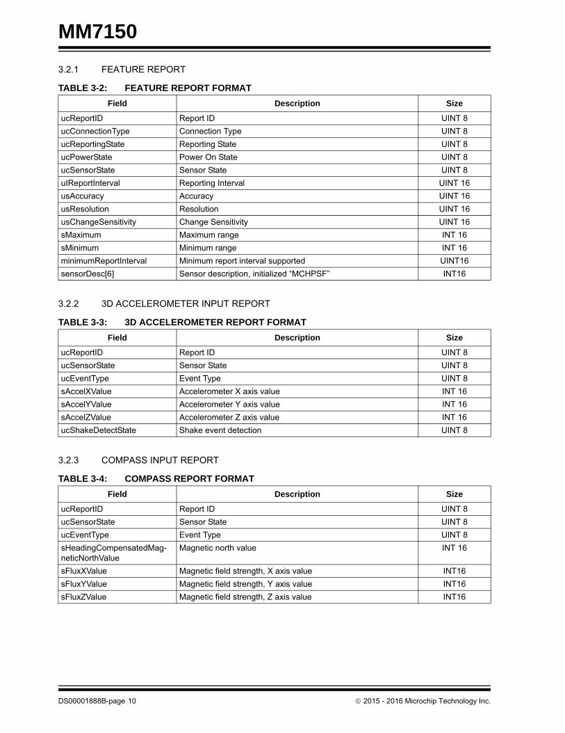
3.2.1 FEATURE REPORT
3.2.2 3D ACCELEROMETER INPUT REPORT
3.2.3 COMPASS INPUT REPORT
TABLE 3-2: FEATURE REPORT FORMAT
Field Description Size
ucReportID Report ID UINT 8
ucConnectionType Connection Type UINT 8
ucReportingState Reporting State UINT 8
ucPowerState Power On State UINT 8
ucSensorState Sensor State UINT 8
uIReportInterval Reporting Interval UINT 16
usAccuracy Accuracy UINT 16
usResolution Resolution UINT 16
usChangeSensitivity Change Sensitivity UINT 16
sMaximum Maximum range INT 16
sMinimum Minimum range INT 16
minimumReportInterval Minimum report interval supported UINT16
sensorDesc[6] Sensor description, initialized “MCHPSF” INT16
TABLE 3-3: 3D ACCELEROMETER REPORT FORMAT
Field Description Size
ucReportID Report ID UINT 8
ucSensorState Sensor State UINT 8
ucEventType Event Type UINT 8
sAccelXValue Accelerometer X axis value INT 16
sAccelYValue Accelerometer Y axis value INT 16
sAccelZValue Accelerometer Z axis value INT 16
ucShakeDetectState Shake event detection UINT 8
TABLE 3-4: COMPASS REPORT FORMAT
Field Description Size
ucReportID Report ID UINT 8
ucSensorState Sensor State UINT 8
ucEventType Event Type UINT 8
sHeadingCompensatedMag-neticNorthValue
Magnetic north value INT 16
sFluxXValue Magnetic field strength, X axis value INT16
sFluxYValue Magnetic field strength, Y axis value INT16
sFluxZValue Magnetic field strength, Z axis value INT16
DS00001888B-page 10 2015 - 2016 Microchip Technology Inc.

MM7150
3.2.4 3D GYROSCOPE INPUT REPORT
3.2.5 INCLINOMETER INPUT REPORT
3.2.6 ORIENTATION INPUT REPORT
TABLE 3-5: 3D GYROSCOPE REPORT FORMAT
Field Description Size
ucReportID Report ID UINT 8
ucSensorState Sensor State UINT 8
ucEventType Event Type UINT 8
sGyroXValue Gyroscope X axis value INT 16
sGyroYValue Gyroscope Y axis value INT 16
sGyroZValue Gyroscope Z axis value INT 16
ucShakeDetectState Shake event detection UINT 8
TABLE 3-6: INCLINOMETER REPORT FORMAT
Field Description Size
ucReportID Report ID UINT 8
ucSensorState Sensor State UINT 8
ucEventType Event Type UINT 8
sIncXValue Inclinometer X axis values INT 16
sIncYValue Inclinometer Y axis value INT 16
sIncZValue Inclinometer Z axis value INT 16
TABLE 3-7: ORIENTATION REPORT FORMAT
Field Description Size
ucReportID Report ID UINT 8
ucSensorState Sensor State UINT 8
ucEventType Event Type UINT 8
sOriXValue Orientation X axis value INT 16
sOriYValue Orientation Y axis value INT 16
sOriZValue Orientation Z axis value INT 16
sOriWValue Orientation W axis value INT 16
2015 - 2016 Microchip Technology Inc. DS00001888B-page 11
MM7150
DS00001888B-page 12 2015 - 2016 Microchip Technology Inc.
4.0 MM7150 HOST INTERFACE
4.1 I2C
The MM7150 can be connected to a host via the I2C interface. The I2C interface is compliant with the I2C standarddescribed in [4], at speeds up to 400KHz. Above the transport layer, the protocol used by the MM7150 is the same HIDprotocol used when communicating over USB. The mapping of HID over I2C is defined in Reference [3]. The protocoland the interface, taken together, are compliant with Windows 8/8.1 certification.

2015 - 2016 Microchip Technology Inc. DS00001888B-page 13
MM7150
5.0 MM7150 FIRMWARE UPDATE
The firmware in the MM7150 Module may be updated at run time. See Reference [5.] for details.

MM7150
DS00001888B-page 14 2015 - 2016 Microchip Technology Inc.
6.0 MM7150 REFERENCES
1. USB-Sig, “Device Class Definition for Human Interface Devices (HID). Firmware Specification”, Version 1.11,6/27/01
2. USB-Sig, “HID Usage Table Sensor Page”, Request HUTRR39, http://www.usb.org/developers/hid-page/HUTRR39b.pdf
3. Microsoft Corporation, “HID Over I2C Protocol Specification: Device Side”, version 1.00, 04/24/2012
4. NXP Corporation, “I2C-bus Specification and User Manual”, Rev. 6, 04/04/2014
5. Microchip Technology Inc., “MM7150 Motion Module User's Guide”, 2014

2015 - 2016 Microchip Technology Inc. DS00001888B-page 15
MM7150
7.0 MM7150 PERFORMANCE
TABLE 7-1: PERFORMANCE PARAMETERS
Parameter Typical
Accelerometer
Range ±2G
Resolution 0.98mG
Accuracy ±40mG
Magnetometer
Range X,Y: ±1300μTZ: ±2500μT
Resolution 0.3μT
Heading Accuracy ±3°
Compass
Range 0° to 360°
Resolution 1°
Accuracy ±10°
Gyroscope
Range ±2000°/s
Resolution 0.061°/s
Accuracy ±5°/s
Inclinometer
Range: Pitch -180° to +180°
Range: Roll -90° to +90°
Range: Yaw 0° to +360°
Resolution 1°
Accuracy ±5°
Orientation - Quaternion
Range ±1.0
Resolution 0.001
Accuracy ±5°

MM7150
8.0 ELECTRICAL CHARACTERISTICS
This section provides an overview of the MM7150 electrical characteristics. Additional information will be provided infuture revisions of this document as it becomes available.
Absolute maximum ratings for the MM7150 devices are listed below. Exposure to these maximum rating conditions forextended periods may affect device reliability. Functional operation of the device at these or any other conditions, abovethe parameters indicated in the operation listings of this specification, is not implied.
Absolute Maximum Ratings
(See Note 1)
Ambient temperature under bias (Commercial temperature range)............................................................ .0°C to +70°C
Ambient temperature under bias (Industrial temperature range) ..............................................................-40°C to +85°C
Storage temperature .............................................................................................................................. -65°C to +150°C
Voltage on VDD with respect to VSS ......................................................................................................... -0.3V to +4.0V
Voltage on any pin that is not 5V tolerant, with respect to VSS (Note 3) ......................................... -0.3V to (VDD + 0.3V)
Voltage on any 5V tolerant pin with respect to VSS when VDD 2.3V (Note 3) ........................................ -0.3V to +5.5V
Voltage on any 5V tolerant pin with respect to VSS when VDD < 2.3V (Note 3) ........................................ -0.3V to +3.6V
Maximum current out of VSS pin(s) .......................................................................................................................300 mA
Maximum current into VDD pin(s) (Note 2)............................................................................................................300 mA
Maximum output current sunk by any I/O pin..........................................................................................................15 mA
Maximum output current sourced by any I/O pin.....................................................................................................15 mA
Maximum current sunk by all ports........................................................................................................................200 mA
Maximum current sourced by all ports (Note 2) ....................................................................................................200 mA
Note 1: Stresses above those listed under “Absolute Maximum Ratings” may cause permanent damage to thedevice. This is a stress rating only and functional operation of the device at those or any other conditions,above those indicated in the operation listings of this specification, is not implied. Exposure to maximumrating conditions for extended periods may affect device reliability.
2: Maximum allowable current is a function of device maximum power dissipation (see Table 8-2).
3: See the “Pin List” section for the 5V tolerant pins.
DS00001888B-page 16 2015 - 2016 Microchip Technology Inc.

MM7150
8.1 DC Characteristics
TABLE 8-2: DC CHARACTERISTICS: OPERATING/POWER-DOWN CURRENT
TABLE 8-1: DC TEMPERATURE AND VOLTAGE SPECIFICATIONS
DC CHARACTERISTICS Standard Operating Conditions: 2.3V to 3.6V(unless otherwise stated)Commercial Operating temperature 0°C TA +70°CIndustrial Operating temperature -40°C TA +85°C
Param. No.
Symbol Characteristics Min. Typ. Max. Units Conditions
Operating Voltage
DC10 VDD Supply Voltage (Note 2) 2.3 — 3.6 V —
DC12 VDR RAM Data Retention Voltage (Note 1)
1.75 — — V —
DC16 VPOR VDD Start Voltageto Ensure Internal Power-on Reset Signal
1.75 — 2.1 V —
DC17 SVDD VDD Rise Rateto Ensure Internal Power-on Reset Signal
0.00005 — 0.115 V/s —
Note 1: This is the limit to which VDD can be lowered without losing RAM data.
2: Overall functional device operation at VBORMIN < VDD < VDDMIN is tested, but not characterized. Refer to parameter BO10 in Table 8-5 for BOR values.
DC CHARACTERISTICS Standard Operating Conditions: 2.3V to 3.6V(unless otherwise stated)Commercial Operating temperature 0°C TA +70°CIndustrial Operating temperature -40°C TA +85°C
Parameter No.
Symbol Typical Max. Units Conditions
Operating/Power-Down Current (Note 1, 2)
DC20 IDD 26.5 mA —
DC30 IAVG 13.65 mA —
DC40 IIDLE 2.5 mA —
DC50 IPD 70 150 μA 0°C TA +70°C
DC50 IPD 120 180 μA -40°C TA +85°C
Note 1: A device’s supply current is mainly a function of the operating voltage and frequency, as well as tempera-ture.
2: The current measurements are as follows:
• Operating current (IDD): This is the peak active current value.
• Average current (IAVG): This value represents an average current measurement of active and low power mode time intervals during operation
measured over 1 second period.
• Idle current (IIDLE)This is the average idle current value when no sensor is actively providing environmental changes (and the device is
not in power-down mode).
• Power-Down current (IPD):This value is the current measured in power-down mode. This is the sleep state entered when the Host issues the
SET_POWER (Sleep) Command if the I2C host interface is used.Wakeup from power-down mode requires the HOST_TO_SH_WAKE pin if the I2C host interface is used.
2015 - 2016 Microchip Technology Inc. DS00001888B-page 17

MM7150
TABLE 8-3: DC CHARACTERISTICS: I/O PIN INPUT SPECIFICATIONS
DC CHARACTERISTICS Standard Operating Conditions: 2.3V to 3.6V (unless otherwise stated)Commercial Operating temperature 0°C TA +70°CIndustrial Operating temperature -40°C TA +85°C
Param. No.
Symbol Characteristics Min. Typical(1) Max. Units Conditions
VIL Input Low Voltage
DI10 I/O Pins VSS — 0.2 VDD V
DI18 SDAx, SCLx VSS — 0.3 VDD V I2C disabled (Note 4)
DI19 SDAx, SCLx VSS — 0.8 V I2C enabled (Note 4)
VIH Input High Voltage
DI20 I/O Pins not 5V-tolerant(5) 0.65 VDD — VDD V (Note 4,6)
I/O Pins 5V-tolerant(5) 0.65 VDD — 5.5 V
DI28 SDAx, SCLx 0.65 VDD — 5.5 V I2C disabled (Note 4,6)
DI29 SDAx, SCLx 2.1 — 5.5 V I2C enabled, 2.3V VPIN 5.5 (Note 4,6)
IIL Input Leakage Current (Note 3)
DI50 I/O Ports — — +1 A VSS VPIN VDD,Pin at high-impedance
DI55 MCLR#(2) — — +1 A VSS VPIN VDD
Note 1: Data in “Typical” column is at 3.3V, 25°C unless otherwise stated. Parameters are for design guidance only and are not tested.
2: The leakage current on the MCLR# pin is strongly dependent on the applied voltage level. The specified levels represent normal operating conditions. Higher leakage current may be measured at different input voltages.
3: Negative current is defined as current sourced by the pin.
4: This parameter is characterized, but not tested in manufacturing.
5: See the “Pin List” section for the 5V-tolerant pins.
6: The VIH specifications are only in relation to externally applied inputs, and not with respect to the user-selectable internal pull-ups. External open drain input signals utilizing the internal pull-ups of the device are ensured to be recognized only as a logic “high” internally to the device. For External “input” logic inputs that require a pull-up source, to ensure the minimum VIH of those components, it is recommended to use an external pull-up resistor rather than the internal pull-ups of the device.
DS00001888B-page 18 2015 - 2016 Microchip Technology Inc.

MM7150
TABLE 8-4: DC CHARACTERISTICS: I/O PIN OUTPUT SPECIFICATIONS
DC CHARACTERISTICS Standard Operating Conditions: 2.3V to 3.6V(unless otherwise stated)Commercial Operating temperature 0°C TA +70°CIndustrial Operating temperature -40°C TA +85°C
Param. Symbol Characteristic Min. Typ. Max. Units Conditions
DO10 Vol Output Low Voltage
I/O Pins
— — 0.4 V IOL 10 mA, VDD = 3.3V
DO20 VOH Output High Voltage
I/O Pins
1.5(1) — — V IOH -14 mA, VDD = 3.3V
2.0(1) — — IOH -12 mA, VDD = 3.3V
2.4 — — IOH -10 mA, VDD = 3.3V
3.0(1) — — IOH -7 mA, VDD = 3.3V
Note 1: Parameters are characterized, but not tested.
TABLE 8-5: ELECTRICAL CHARACTERISTICS: BROWN-OUT RESET (BOR)
DC CHARACTERISTICS Standard Operating Conditions: 2.3V to 3.6V(unless otherwise stated)Commercial Operating temperature 0°C TA +70°CIndustrial Operating temperature -40°C TA +85°C
Param.No.
Symbol Characteristics Min.(1) Typical Max. Units Conditions
BO10 Vbor BOR Event on VDD transition high-to-low(2)
2.0 — 2.3 V —
Note 1: Parameters are for design guidance only and are not tested in manufacturing.
2: Overall functional device operation at VBORMIN < VDD < VDDMIN is tested, but not characterized.
TABLE 8-6: INTERNAL VOLTAGE REGULATOR SPECIFICATIONS
DC CHARACTERISTICS
Standard Operating Conditions: 2.3V to 3.6V(unless otherwise stated)Commercial Operating temperature 0°C TA +70°CIndustrial Operating temperature -40°C TA +85°C
Param.No.
Symbol Characteristics Min. Typical Max. Units Comments
D321 Cefc External Filter Capacitor Value 8 10 — F Capacitor must be low series resistance (1 ohm). Typical voltage on the VCAP pin is 1.8V.
2015 - 2016 Microchip Technology Inc. DS00001888B-page 19

MM7150
8.2 AC Characteristics and Timing Parameters
The information contained in this section defines MM7150 AC characteristics and timing parameters.
FIGURE 8-1: LOAD CONDITIONS FOR DEVICE TIMING SPECIFICATIONS
TABLE 8-7: CAPACITIVE LOADING REQUIREMENTS ON OUTPUT PINS
AC CHARACTERISTICSStandard Operating Conditions: 2.3V to 3.6V(unless otherwise stated)
Param. No.
Symbol Characteristics Min. Typical(1) Max. Units Conditions
DO56 CIO All I/O pins — — 50 pF
DO58 CB SCLx, SDAx — — 400 pF In I2C™ mode
Note 1: Data in “Typical” column is at 3.3V, 25°C unless otherwise stated. Parameters are for design guidance only and are not tested.
VDD/2
CL
RL
Pin
Pin
VSS
VSS
CL
RL = 464
CL = 50 pF for all pins
Load Condition 1 – for all pins except OSC2 Load Condition 2 – for OSC2
DS00001888B-page 20 2015 - 2016 Microchip Technology Inc.
MM7150
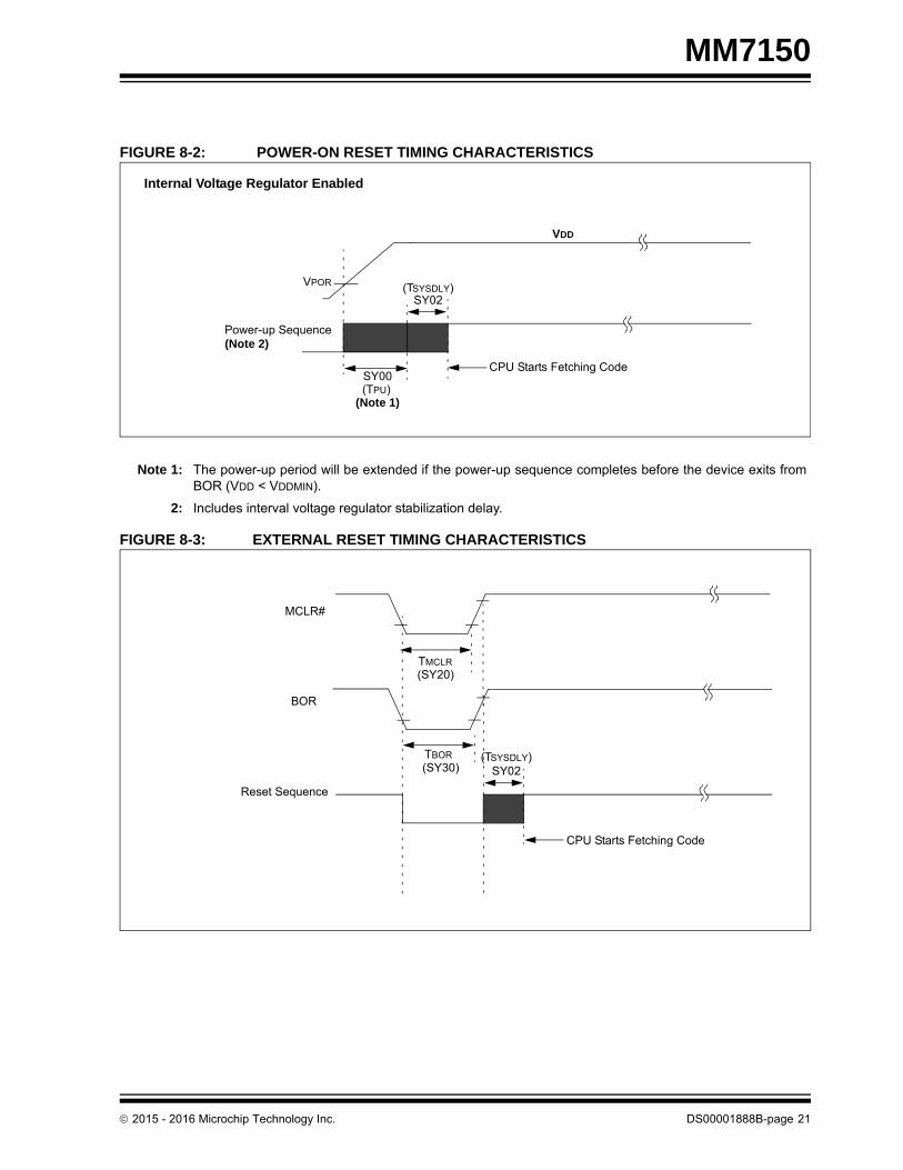
FIGURE 8-2: POWER-ON RESET TIMING CHARACTERISTICS
FIGURE 8-3: EXTERNAL RESET TIMING CHARACTERISTICS
Note 1: The power-up period will be extended if the power-up sequence completes before the device exits fromBOR (VDD < VDDMIN).
2: Includes interval voltage regulator stabilization delay.
Internal Voltage Regulator Enabled
VDD
VPOR
SY00
Power-up Sequence(Note 2)
Internal Voltage Regulator Enabled
(TPU)
(TSYSDLY)
CPU Starts Fetching Code
(Note 1)
Clock Sources = (FRC, FRCDIV, FRCDIV16, FRCPLL, EC, ECPLL and LPRC)
SY02
MCLR#
(SY20)
BOR
(SY30)
TMCLR
TBOR
Reset Sequence
CPU Starts Fetching Code
Clock Sources = (FRC, FRCDIV, FRCDIV16, FRCPLL, EC, ECPLL and LPRC)
Clock Sources = (HS, HSPLL, XT, XTPLL and SOSC) (TSYSDLY)SY02
(TSYSDLY)SY02
2015 - 2016 Microchip Technology Inc. DS00001888B-page 21

MM7150
TABLE 8-8: RESETS TIMING
FIGURE 8-4: I2Cx BUS START/STOP BITS TIMING CHARACTERISTICS (SLAVE MODE)
FIGURE 8-5: I2Cx BUS DATA TIMING CHARACTERISTICS (SLAVE MODE)
AC CHARACTERISTICS Standard Operating Conditions: 2.3V to 3.6V(unless otherwise stated)
Param.No.
Symbol Characteristics(1) Min. Typical(2) Max. Units Conditions
SY00 TPU Power-up PeriodInternal Voltage Regulator Enabled
— 400 600 s —
SY02 Tsysdly System Delay Period:Time Required to Reload Device Configuration Fuses plus SYSCLK(3) Delay before First instruction is Fetched.
— s + 8 SYSCLK
cycles
— — —
SY20 Tmclr MCLR# Pulse Width (low) 2 — — s —
SY30 TBOR BOR Pulse Width (low) — 1 — s —
Note 1: These parameters are characterized, but not tested in manufacturing.
2: Data in “Typ” column is at 3.3V, 25°C unless otherwise stated. Characterized by design but not tested.
3: SYSCLK is 48MHz
IS34SCLx
SDAx
StartCondition
StopCondition
IS33
Note: Refer to Figure 8-1 for load conditions.
IS31
IS30
IS30IS31 IS33
IS11
IS10
IS20
IS26IS25
IS40 IS40 IS45
IS21
SCLx
SDAxIn
SDAxOut
Note: Refer to Figure 8-1 for load conditions.
DS00001888B-page 22 2015 - 2016 Microchip Technology Inc.

MM7150
TABLE 8-9: I2Cx BUS DATA TIMING REQUIREMENTS (SLAVE MODE)
AC CHARACTERISTICSStandard Operating Conditions: 2.3V to 3.6V
(unless otherwise stated)
Param. No.
Symbol Characteristics Min. Max. Units Conditions
IS10 TLO:SCL Clock Low Time 100 kHz mode 4.7 — s —
400 kHz mode 1.3 — s —
IS11 THI:SCL Clock High Time 100 kHz mode 4.0 — s —
400 kHz mode 0.6 — s —
IS20 TF:SCL SDAx and SCLxFall Time
100 kHz mode — 300 ns CB is specified to be from10 to 400 pF
400 kHz mode 20 + 0.1 CB 300 ns
IS21 TR:SCL SDAx and SCLxRise Time
100 kHz mode — 1000 ns CB is specified to be from10 to 400 pF
400 kHz mode 20 + 0.1 CB 300 ns
IS25 TSU:DAT Data InputSetup Time
100 kHz mode 250 — ns —
400 kHz mode 100 — ns
IS26 THD:DAT Data InputHold Time
100 kHz mode 0 — ns —
400 kHz mode 0 0.9 s
IS30 TSU:STA Start ConditionSetup Time
100 kHz mode 4700 — ns Only relevant for Repeated Start condition
400 kHz mode 600 — ns
IS31 THD:STA Start Condition Hold Time
100 kHz mode 4000 — ns After this period, the first clock pulse is generated
400 kHz mode 600 — ns
IS33 TSU:STO Stop Condition Setup Time
100 kHz mode 4000 — ns —
400 kHz mode 600 — ns
IS34 THD:STO Stop ConditionHold Time
100 kHz mode 4000 — ns —
400 kHz mode 600 — ns
IS40 TAA:SCL Output Valid from Clock
100 kHz mode 0 3500 ns —
400 kHz mode 0 1000 ns
IS45 TBF:SDA Bus Free Time 100 kHz mode 4.7 — s The amount of time the bus must be free before a new transmission can start
400 kHz mode 1.3 — s
IS50 CB Bus Capacitive Loading
— 400 pF —
2015 - 2016 Microchip Technology Inc. DS00001888B-page 23

MM7150
DS00001888B-page 24 2015 - 2016 Microchip Technology Inc.
APPENDIX A: REVISION HISTORY
TABLE A-1: REVISION HISTORY
Revision Section/Figure/Entry Correction
DS00001888B (01-26-16) Industrial Temp Range Added Industrial Temp Range to Data Sheet
Updated IPD for Industrial Temp Range
DS00001888A (02-05-15) Initial Release
2015 - 2016 Microchip Technology Inc. DS00001888B-page 25
MM7150
THE MICROCHIP WEB SITE
Microchip provides online support via our WWW site at www.microchip.com. This web site is used as a means to makefiles and information easily available to customers. Accessible by using your favorite Internet browser, the web site con-tains the following information:
• Product Support – Data sheets and errata, application notes and sample programs, design resources, user’s guides and hardware support documents, latest software releases and archived software
• General Technical Support – Frequently Asked Questions (FAQ), technical support requests, online discussion groups, Microchip consultant program member listing
• Business of Microchip – Product selector and ordering guides, latest Microchip press releases, listing of semi-nars and events, listings of Microchip sales offices, distributors and factory representatives
CUSTOMER CHANGE NOTIFICATION SERVICE
Microchip’s customer notification service helps keep customers current on Microchip products. Subscribers will receivee-mail notification whenever there are changes, updates, revisions or errata related to a specified product family ordevelopment tool of interest.
To register, access the Microchip web site at www.microchip.com. Under “Support”, click on “Customer Change Notifi-cation” and follow the registration instructions.
CUSTOMER SUPPORT
Users of Microchip products can receive assistance through several channels:
• Distributor or Representative
• Local Sales Office
• Field Application Engineer (FAE)
• Technical Support
Customers should contact their distributor, representative or field application engineer (FAE) for support. Local salesoffices are also available to help customers. A listing of sales offices and locations is included in the back of this docu-ment.
Technical support is available through the web site at: http://microchip.com/support
MM7150
DS00001888B-page 26 2015 - 2016 Microchip Technology Inc.
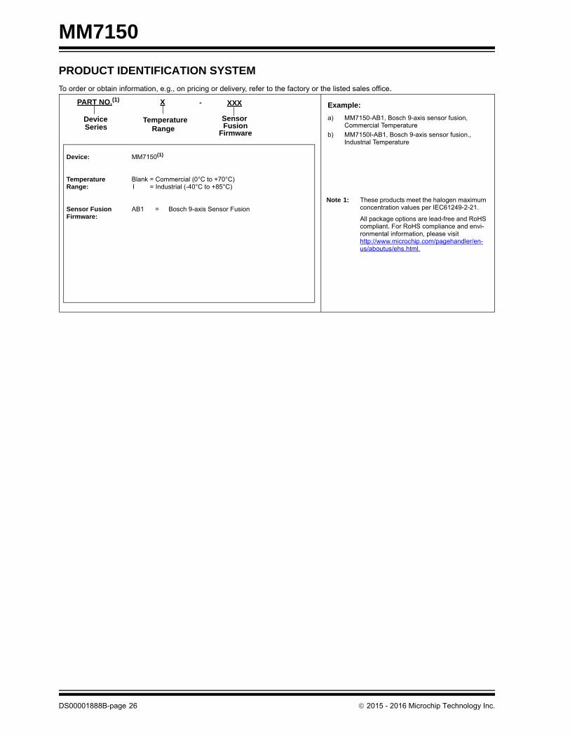
PRODUCT IDENTIFICATION SYSTEM
To order or obtain information, e.g., on pricing or delivery, refer to the factory or the listed sales office.
PART NO.(1) X
Device
Device: MM7150(1)
TemperatureRange:
Blank = Commercial (0°C to +70°C)I = Industrial (-40°C to +85°C)
Sensor Fusion Firmware:
AB1 = Bosch 9-axis Sensor Fusion
Example:
a) MM7150-AB1, Bosch 9-axis sensor fusion, Commercial Temperature
b) MM7150I-AB1, Bosch 9-axis sensor fusion., Industrial Temperature
Series
All package options are lead-free and RoHS compliant. For RoHS compliance and envi-ronmental information, please visit http://www.microchip.com/pagehandler/en-us/aboutus/ehs.html.
Note 1: These products meet the halogen maximum concentration values per IEC61249-2-21.
XXX
FirmwareFusionSensorTemperature
Range
-

2015 - 2016 Microchip Technology Inc. DS00001888B-page 27
MM7150
Information contained in this publication regarding device applications and the like is provided only for your convenience and may be super-seded by updates. It is your responsibility to ensure that your application meets with your specifications. MICROCHIP MAKES NO REP-RESENTATIONS OR WARRANTIES OF ANY KIND WHETHER EXPRESS OR IMPLIED, WRITTEN OR ORAL, STATUTORY OROTHERWISE, RELATED TO THE INFORMATION, INCLUDING BUT NOT LIMITED TO ITS CONDITION, QUALITY, PERFORMANCE,MERCHANTABILITY OR FITNESS FOR PURPOSE. Microchip disclaims all liability arising from this information and its use. Use of Micro-chip devices in life support and/or safety applications is entirely at the buyer’s risk, and the buyer agrees to defend, indemnify and holdharmless Microchip from any and all damages, claims, suits, or expenses resulting from such use. No licenses are conveyed, implicitly orotherwise, under any Microchip intellectual property rights unless otherwise stated.
Trademarks
The Microchip name and logo, the Microchip logo, AnyRate, dsPIC, FlashFlex, flexPWR, Heldo, JukeBlox, KeeLoq, KeeLoq logo, Kleer, LANCheck, LINK MD, MediaLB, MOST, MOST logo, MPLAB, OptoLyzer, PIC, PICSTART, PIC32 logo, RightTouch, SpyNIC, SST, SST Logo, SuperFlash and UNI/O are registered trademarks of Microchip Technology Incorporated in the U.S.A. and other countries.
ClockWorks, The Embedded Control Solutions Company, ETHERSYNCH, Hyper Speed Control, HyperLight Load, IntelliMOS, mTouch, Precision Edge, and QUIET-WIRE are registered trademarks of Microchip Technology Incorporated in the U.S.A.
Analog-for-the-Digital Age, Any Capacitor, AnyIn, AnyOut, BodyCom, chipKIT, chipKIT logo, CodeGuard, dsPICDEM, dsPICDEM.net, Dynamic Average Matching, DAM, ECAN, EtherGREEN, In-Circuit Serial Programming, ICSP, Inter-Chip Connectivity, JitterBlocker, KleerNet, KleerNet logo, MiWi, motorBench, MPASM, MPF, MPLAB Certified logo, MPLIB, MPLINK, MultiTRAK, NetDetach, Omniscient Code Generation, PICDEM, PICDEM.net, PICkit, PICtail, PureSilicon, RightTouch logo, REAL ICE, Ripple Blocker, Serial Quad I/O, SQI, SuperSwitcher, SuperSwitcher II, Total Endurance, TSHARC, USBCheck, VariSense, ViewSpan, WiperLock, Wireless DNA, and ZENA are trademarks of Microchip Technology Incorporated in the U.S.A. and other countries.
SQTP is a service mark of Microchip Technology Incorporated in the U.S.A.
Silicon Storage Technology is a registered trademark of Microchip Technology Inc. in other countries.
GestIC is a registered trademarks of Microchip Technology Germany II GmbH & Co. KG, a subsidiary of Microchip Technology Inc., in other countries.
All other trademarks mentioned herein are property of their respective companies.
© 2015 - 2016, Microchip Technology Incorporated, Printed in the U.S.A., All Rights Reserved.
ISBN: 9781522402169
Note the following details of the code protection feature on Microchip devices:
• Microchip products meet the specification contained in their particular Microchip Data Sheet.
• Microchip believes that its family of products is one of the most secure families of its kind on the market today, when used in the intended manner and under normal conditions.
• There are dishonest and possibly illegal methods used to breach the code protection feature. All of these methods, to our knowledge, require using the Microchip products in a manner outside the operating specifications contained in Microchip’s Data Sheets. Most likely, the person doing so is engaged in theft of intellectual property.
• Microchip is willing to work with the customer who is concerned about the integrity of their code.
• Neither Microchip nor any other semiconductor manufacturer can guarantee the security of their code. Code protection does not mean that we are guaranteeing the product as “unbreakable.”
Code protection is constantly evolving. We at Microchip are committed to continuously improving the code protection features of ourproducts. Attempts to break Microchip’s code protection feature may be a violation of the Digital Millennium Copyright Act. If such actsallow unauthorized access to your software or other copyrighted work, you may have a right to sue for relief under that Act.
Microchip received ISO/TS-16949:2009 certification for its worldwide headquarters, design and wafer fabrication facilities in Chandler and Tempe, Arizona; Gresham, Oregon and design centers in California and India. The Company’s quality system processes and procedures are for its PIC® MCUs and dsPIC® DSCs, KEELOQ® code hopping devices, Serial EEPROMs, microperipherals, nonvolatile memory and analog products. In addition, Microchip’s quality system for the design and manufacture of development systems is ISO 9001:2000 certified.
QUALITYMANAGEMENTSYSTEMCERTIFIEDBYDNV
== ISO/TS16949==

DS00001888B-page 28 2015 - 2016 Microchip Technology Inc.
AMERICASCorporate Office2355 West Chandler Blvd.Chandler, AZ 85224-6199Tel: 480-792-7200 Fax: 480-792-7277Technical Support: http://www.microchip.com/supportWeb Address: www.microchip.com
AtlantaDuluth, GA Tel: 678-957-9614 Fax: 678-957-1455
Austin, TXTel: 512-257-3370
BostonWestborough, MA Tel: 774-760-0087 Fax: 774-760-0088
ChicagoItasca, IL Tel: 630-285-0071 Fax: 630-285-0075
ClevelandIndependence, OH Tel: 216-447-0464 Fax: 216-447-0643
DallasAddison, TX Tel: 972-818-7423 Fax: 972-818-2924
DetroitNovi, MI Tel: 248-848-4000
Houston, TX Tel: 281-894-5983
IndianapolisNoblesville, IN Tel: 317-773-8323Fax: 317-773-5453
Los AngelesMission Viejo, CA Tel: 949-462-9523 Fax: 949-462-9608
New York, NY Tel: 631-435-6000
San Jose, CA Tel: 408-735-9110
Canada - TorontoTel: 905-673-0699 Fax: 905-673-6509
ASIA/PACIFICAsia Pacific OfficeSuites 3707-14, 37th FloorTower 6, The GatewayHarbour City, Kowloon
Hong KongTel: 852-2943-5100Fax: 852-2401-3431
Australia - SydneyTel: 61-2-9868-6733Fax: 61-2-9868-6755
China - BeijingTel: 86-10-8569-7000 Fax: 86-10-8528-2104
China - ChengduTel: 86-28-8665-5511Fax: 86-28-8665-7889
China - ChongqingTel: 86-23-8980-9588Fax: 86-23-8980-9500
China - DongguanTel: 86-769-8702-9880
China - HangzhouTel: 86-571-8792-8115 Fax: 86-571-8792-8116
China - Hong Kong SARTel: 852-2943-5100 Fax: 852-2401-3431
China - NanjingTel: 86-25-8473-2460Fax: 86-25-8473-2470
China - QingdaoTel: 86-532-8502-7355Fax: 86-532-8502-7205
China - ShanghaiTel: 86-21-5407-5533 Fax: 86-21-5407-5066
China - ShenyangTel: 86-24-2334-2829Fax: 86-24-2334-2393
China - ShenzhenTel: 86-755-8864-2200 Fax: 86-755-8203-1760
China - WuhanTel: 86-27-5980-5300Fax: 86-27-5980-5118
China - XianTel: 86-29-8833-7252Fax: 86-29-8833-7256
ASIA/PACIFICChina - XiamenTel: 86-592-2388138 Fax: 86-592-2388130
China - ZhuhaiTel: 86-756-3210040 Fax: 86-756-3210049
India - BangaloreTel: 91-80-3090-4444 Fax: 91-80-3090-4123
India - New DelhiTel: 91-11-4160-8631Fax: 91-11-4160-8632
India - PuneTel: 91-20-3019-1500
Japan - OsakaTel: 81-6-6152-7160 Fax: 81-6-6152-9310
Japan - TokyoTel: 81-3-6880- 3770 Fax: 81-3-6880-3771
Korea - DaeguTel: 82-53-744-4301Fax: 82-53-744-4302
Korea - SeoulTel: 82-2-554-7200Fax: 82-2-558-5932 or 82-2-558-5934
Malaysia - Kuala LumpurTel: 60-3-6201-9857Fax: 60-3-6201-9859
Malaysia - PenangTel: 60-4-227-8870Fax: 60-4-227-4068
Philippines - ManilaTel: 63-2-634-9065Fax: 63-2-634-9069
SingaporeTel: 65-6334-8870Fax: 65-6334-8850
Taiwan - Hsin ChuTel: 886-3-5778-366Fax: 886-3-5770-955
Taiwan - KaohsiungTel: 886-7-213-7828
Taiwan - TaipeiTel: 886-2-2508-8600 Fax: 886-2-2508-0102
Thailand - BangkokTel: 66-2-694-1351Fax: 66-2-694-1350
EUROPEAustria - WelsTel: 43-7242-2244-39Fax: 43-7242-2244-393
Denmark - CopenhagenTel: 45-4450-2828 Fax: 45-4485-2829
France - ParisTel: 33-1-69-53-63-20 Fax: 33-1-69-30-90-79
Germany - DusseldorfTel: 49-2129-3766400
Germany - KarlsruheTel: 49-721-625370
Germany - MunichTel: 49-89-627-144-0 Fax: 49-89-627-144-44
Italy - Milan Tel: 39-0331-742611 Fax: 39-0331-466781
Italy - VeniceTel: 39-049-7625286
Netherlands - DrunenTel: 31-416-690399 Fax: 31-416-690340
Poland - WarsawTel: 48-22-3325737
Spain - MadridTel: 34-91-708-08-90Fax: 34-91-708-08-91
Sweden - StockholmTel: 46-8-5090-4654
UK - WokinghamTel: 44-118-921-5800Fax: 44-118-921-5820
Worldwide Sales and Service
07/14/15