mm145453 liquid crystal display driver datasheet … snls061c – may 2000– revised march 2013...
TRANSCRIPT

MM145453
www.ti.com SNLS061C –MAY 2000–REVISED MARCH 2013
MM145453 Liquid Crystal Display DriverCheck for Samples: MM145453
1FEATURES DESCRIPTIONThe MM145453 is a monolithic integrated circuit
2• Serial Data Inpututilizing CMOS metal gate, low threshold
• Wide Power Supply Operation enhancement mode devices. The chip can drive up to• TTL Compatibility 33 LCD segments and can be paralleled to increase
this number. The chip is capable of driving a 4½ digit• Up to 33 LCD Segments7-segment display with minimal interface between the• Alphanumeric or Bar Graph Capability display and the data source.
• Cascaded Operation CapabilityThe MM145453 stores display data in latches after it
• Pin Compatible with MC145453 is clocked in, and holds the data until new displaydata is received.
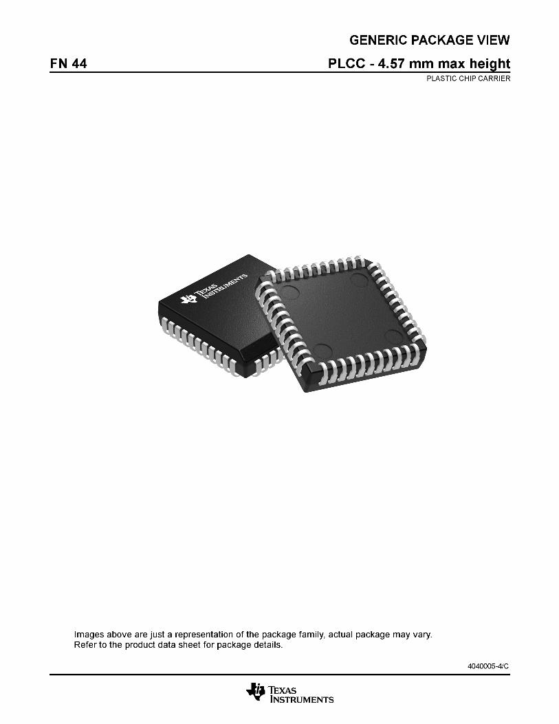
APPLICATIONSThe MM145453 is available in a molded 44 pin
• COPS or Microprocessor Displays surface mount PLCC package. The MM145453 is pin• Industrial Control Indicator out and functionally compatible with the MC145453.• Digital Clock, Thermometer, Counter,
Voltmeter• Instrumentation Displays• Remote Displays
Connection Diagram
Figure 1. Top ViewSee Package Number FN0044A
1
Please be aware that an important notice concerning availability, standard warranty, and use in critical applications ofTexas Instruments semiconductor products and disclaimers thereto appears at the end of this data sheet.
2All trademarks are the property of their respective owners.
PRODUCTION DATA information is current as of publication date. Copyright © 2000–2013, Texas Instruments IncorporatedProducts conform to specifications per the terms of the TexasInstruments standard warranty. Production processing does notnecessarily include testing of all parameters.

MM145453
SNLS061C –MAY 2000–REVISED MARCH 2013 www.ti.com
These devices have limited built-in ESD protection. The leads should be shorted together or the device placed in conductive foamduring storage or handling to prevent electrostatic damage to the MOS gates.
Absolute Maximum Ratings (1) (2)
Voltage at Any Pin, Referenced to Gnd -0.3V to +10V
Storage Temperature -65°C to +150°C
Power Dissipation at 25°C 350mW
Power Dissipation at 70°C 300mW
Junction Temperature +150°C
Lead Temperature (Soldering, 10s) 300°C
(1) “Absolute Maximum Ratings” are those values beyond which the safety of the device cannot be guaranteed. They are not meant toimply that the devices should be operated at these limits. The table of “Electrical Characteristics” specifies conditions of deviceoperation.
(2) If Military/Aerospace specified devices are required, please contact the TI Sales Office/ Distributors for availability and specifications.
Recommended Operating ConditionsVDD 3V to 10V
Operating Temperature −40°C to 85°C
Electrical CharacteristicsThe following specifications apply for TA within operation range, VDD = 3.0V to 10V, VSS = 0V, unless otherwise specified.
Parameter Conditions Min Typical Max Units
Supply Voltage, VDD 3 10 V
Average Supply Current, IDD All Outputs Open, Clock=Gnd,Data=Gnd,OSC=Gnd, BP_IN @ 32Hz
VDD= 5V 10 µA
VDD= 10V 40 µA
Input Logical '0' Voltage, VIL VDD= 3V 0.4 V
VDD= 5V 0.8 V
VDD= 10V 0.8 V
Input Logical '1' Voltage, VIH VDD= 3V 2.0 V
VDD= 5V 2.0 V
VDD= 10V 8.0 V
Segment Sink Current, IOL VDD= 3V, VOUT= 0.3V -20 -40 µA
Segment Source Current, IOH VDD= 3V, VOUT= 2.7V 20 40 µA
Backplane Out Sink Current, IOL VDD= 3V, VOUT= 0.3V -320 -500 µA
Backplane Out Source Current, VDD= 3V, VOUT= 2.7V 320 500 µAIOH
Segment Output Offset Voltage Segment Load = 250pF (1) +/-50 mV
Backplane Output Offset Voltage Backplane Load = 8750pF (1) +/-50 mV
Backplane Out Frequency ROSC_IN= 50kΩ, COSC_IN= 0.01µF 75 Hz
Clock Input Frequency, fCLOCK(2) VDD= 3V (1) (3) 500 kHz
VDD= 5V (1) 750 kHz
VDD= 10V (1) 1.0 MHz
Clock Input Duty Cycle (2) 40 60 %
Data Input Set-Up Time, tDS 300 ns
Data Input Hold Time, tDH 300 ns
(1) This parameter is guaranteed (but not production tested) over the operating temperature range and the operating supply voltage range.Not to be used in Q.A. testing.
(2) Clock input rise time (tr) and fall time (tf) must not exceed 300ns(3) AC input waveform for test purposes: tr≤ 20ns, tf≤ 20ns, fCLOCK= 500kHz, Duty Cycle = 50% ±10%
2 Submit Documentation Feedback Copyright © 2000–2013, Texas Instruments Incorporated
Product Folder Links: MM145453
MM145453
www.ti.com SNLS061C –MAY 2000–REVISED MARCH 2013
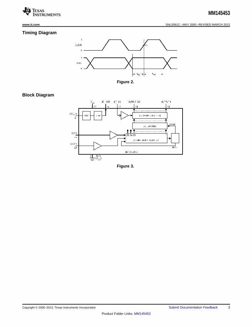
Timing Diagram
Figure 2.
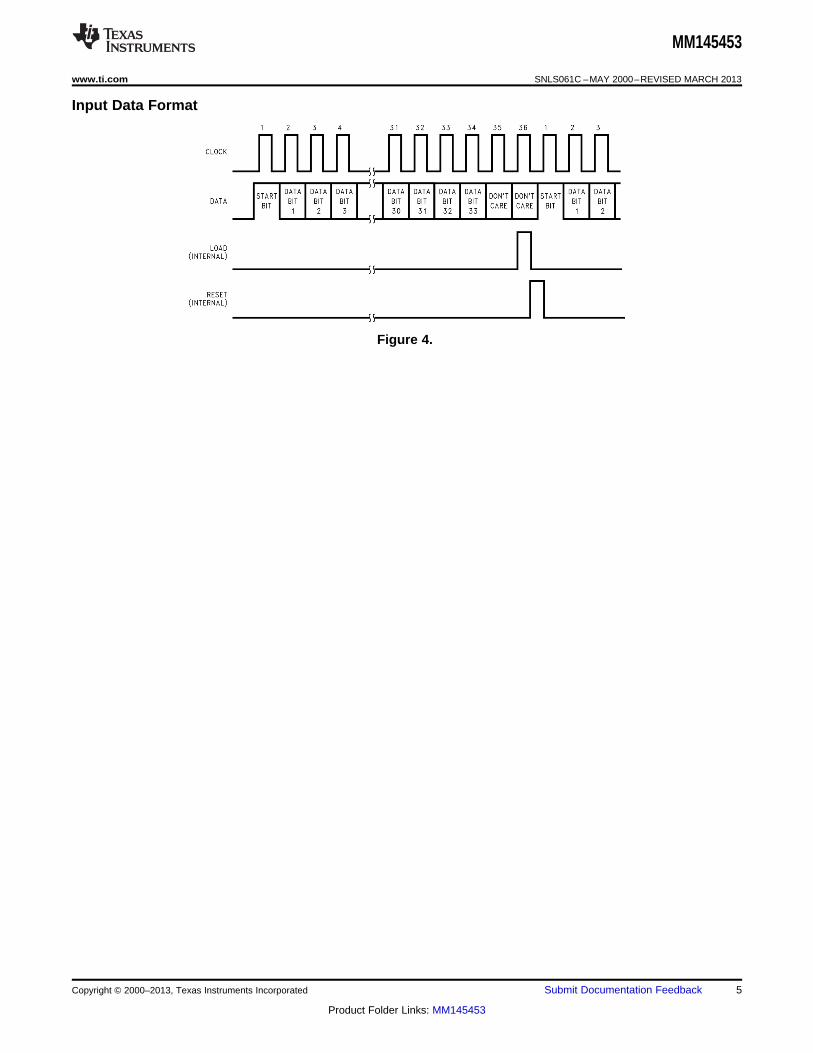
Block Diagram
Figure 3.
Copyright © 2000–2013, Texas Instruments Incorporated Submit Documentation Feedback 3
Product Folder Links: MM145453

MM145453
SNLS061C –MAY 2000–REVISED MARCH 2013 www.ti.com
APPLICATIONS INFORMATION
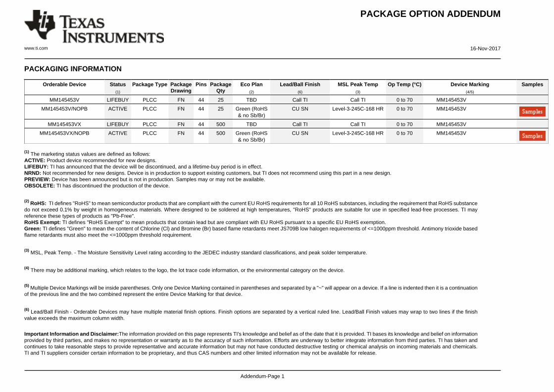
The MM145453 is specifically designed to operate 4½ digit 7-segment displays with minimal interface with thedisplay and data source. Serial data transfer from the data source to the display driver is accomplished with 2signals, serial Data and Clock. Using a format of a leading "1" followed by the 33 data bits and 2 trailing don'tcare bits, allows data transfer without the need of an additional Data Load signal. Since the MM145453 does notcontain a character generator, the formatting of the segment information must be done prior to inputting the datato the MM145453. The transfer of the 33 data bits is complete at the falling edge of the 36th clock cycle, thusproviding non-multiplexed, direct drive to the display. Outputs change only if the serial data bits differ from theprevious time.
Figure 4 shows the data input format. A single start bit of logical '1' precedes the 33 bits of segment data for atotal of 34 bits that need to be defined and clocked in. After the 34 bits are clocked in, 2 additional clock cyclesare required. At the 36th clock cycle an internal LOAD signal is generated synchronously with the rising edge ofthe Clock In signal, which loads the 33 bits of segment data in the shift register into the latches. At the fallingedge of the 36th clock cycle an internal RESET signal is generated which clears all the shift registers for the nextset of data. The shift registers are static master-slave configuration. There is no clear for the master portion ofthe first shift register, thus allowing continuous operation. The data during the 35th and 36th clock cycles is "don'tcare", but setting data to logical '0' for these two clock cycles is the preferred format.
The data input bits map directly to the segment output pins and the display. The MM145453 does not have anyformat restrictions, as all outputs are controllable.
The MM145453 has an internal oscillator which can generate the required clock signal to drive the LCD backplane. The frequency of the internal oscillator is set by a pull-up resistor (ROSC_IN) connected from the OSC_INpin to VDD, and a capacitor (COSC_IN) connected from the OSC_IN pin to Ground. Due to the current sinklimitations of the OSC_IN circuitry, the lowest recommended resistor value for setting the oscillator frequency is9kΩ. It will typically take 2 to 4 RC time constants to charge the OSC_IN pin from near 0V to within 1V of VDDwhich is the high threshold voltage point for the OSC_IN circuitry. An approximate calculation of fOSC is:
fOSC = 1 / (lη(VDD/1V) X ROSC_IN X COSC_IN)
A ROSC_IN resistor value of 50kΩ with a COSC_IN capacitor value of 0.01µF and a VDD value of 5.00V wouldproduce a typical oscillator frequency ( fOSC) of about 1200Hz. The fOSC signal is divided by 16 before it ispresented at the BP_OUT pin. For this example the approximate BP_OUT frequency will be fOSC/16, or about75Hz.
The BP_IN pin of the MM145453 can be used with an externally supplied signal, provided it has a duty cycle of50%. Any deviation from a precise 50% duty cycle will result in an offset voltage on the LCD. The use of anexternal clock allows synchronizing the display drive with AC power, other internal clocks, or DVM integrationtime to reduce interference from the display. When using an external clock for the back plane drive the internaloscillator should be disabled by connecting the OSC_IN pin directly to ground. This will prevent possible internaloscillations, and reduce device dissipation.
The MM145453 is a pin out variation of the MM5453. For additional applications information please refer to theMM5453 data sheet.
4 Submit Documentation Feedback Copyright © 2000–2013, Texas Instruments Incorporated
Product Folder Links: MM145453
MM145453
www.ti.com SNLS061C –MAY 2000–REVISED MARCH 2013
Input Data Format
Figure 4.
Copyright © 2000–2013, Texas Instruments Incorporated Submit Documentation Feedback 5
Product Folder Links: MM145453

MM145453
SNLS061C –MAY 2000–REVISED MARCH 2013 www.ti.com
REVISION HISTORY
Changes from Revision B (March 2013) to Revision C Page
• Changed layout of National Data Sheet to TI format ............................................................................................................ 5
6 Submit Documentation Feedback Copyright © 2000–2013, Texas Instruments Incorporated
Product Folder Links: MM145453
PACKAGE OPTION ADDENDUM
www.ti.com 16-Nov-2017
Addendum-Page 1
PACKAGING INFORMATION
Orderable Device Status(1)
Package Type PackageDrawing
Pins PackageQty
Eco Plan(2)
Lead/Ball Finish(6)
MSL Peak Temp(3)
Op Temp (°C) Device Marking(4/5)
Samples
MM145453V LIFEBUY PLCC FN 44 25 TBD Call TI Call TI 0 to 70 MM145453V
MM145453V/NOPB ACTIVE PLCC FN 44 25 Green (RoHS& no Sb/Br)
CU SN Level-3-245C-168 HR 0 to 70 MM145453V
MM145453VX LIFEBUY PLCC FN 44 500 TBD Call TI Call TI 0 to 70 MM145453V
MM145453VX/NOPB ACTIVE PLCC FN 44 500 Green (RoHS& no Sb/Br)
CU SN Level-3-245C-168 HR 0 to 70 MM145453V
(1) The marketing status values are defined as follows:ACTIVE: Product device recommended for new designs.LIFEBUY: TI has announced that the device will be discontinued, and a lifetime-buy period is in effect.NRND: Not recommended for new designs. Device is in production to support existing customers, but TI does not recommend using this part in a new design.PREVIEW: Device has been announced but is not in production. Samples may or may not be available.OBSOLETE: TI has discontinued the production of the device.
(2) RoHS: TI defines "RoHS" to mean semiconductor products that are compliant with the current EU RoHS requirements for all 10 RoHS substances, including the requirement that RoHS substancedo not exceed 0.1% by weight in homogeneous materials. Where designed to be soldered at high temperatures, "RoHS" products are suitable for use in specified lead-free processes. TI mayreference these types of products as "Pb-Free".RoHS Exempt: TI defines "RoHS Exempt" to mean products that contain lead but are compliant with EU RoHS pursuant to a specific EU RoHS exemption.Green: TI defines "Green" to mean the content of Chlorine (Cl) and Bromine (Br) based flame retardants meet JS709B low halogen requirements of <=1000ppm threshold. Antimony trioxide basedflame retardants must also meet the <=1000ppm threshold requirement.
(3) MSL, Peak Temp. - The Moisture Sensitivity Level rating according to the JEDEC industry standard classifications, and peak solder temperature.
(4) There may be additional marking, which relates to the logo, the lot trace code information, or the environmental category on the device.
(5) Multiple Device Markings will be inside parentheses. Only one Device Marking contained in parentheses and separated by a "~" will appear on a device. If a line is indented then it is a continuationof the previous line and the two combined represent the entire Device Marking for that device.
(6) Lead/Ball Finish - Orderable Devices may have multiple material finish options. Finish options are separated by a vertical ruled line. Lead/Ball Finish values may wrap to two lines if the finishvalue exceeds the maximum column width.
Important Information and Disclaimer:The information provided on this page represents TI's knowledge and belief as of the date that it is provided. TI bases its knowledge and belief on informationprovided by third parties, and makes no representation or warranty as to the accuracy of such information. Efforts are underway to better integrate information from third parties. TI has taken andcontinues to take reasonable steps to provide representative and accurate information but may not have conducted destructive testing or chemical analysis on incoming materials and chemicals.TI and TI suppliers consider certain information to be proprietary, and thus CAS numbers and other limited information may not be available for release.
PACKAGE OPTION ADDENDUM
www.ti.com 16-Nov-2017
Addendum-Page 2
In no event shall TI's liability arising out of such information exceed the total purchase price of the TI part(s) at issue in this document sold by TI to Customer on an annual basis.
www.ti.com
PACKAGE OUTLINE
C
44X -.021.013-0.530.33[ ]
44X -.032.026-0.810.66[ ]
TYP
-.695.685-17.6517.40[ ]
40X .050[1.27]
-.638.582-16.2014.79[ ]
.020 MIN[0.51]
TYP-.120.090-3.042.29[ ]
.180 MAX[4.57]
B
NOTE 3
-.656.650-16.6616.51[ ]
A
NOTE 3
-.656.650-16.6616.51[ ]
(.008)[0.2]
4215154/A 04/2017
4215154/A 04/2017
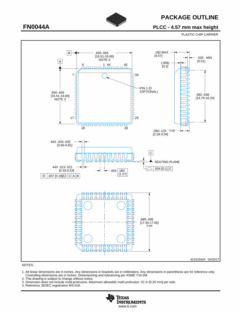
PLCC - 4.57 mm max heightFN0044APLASTIC CHIP CARRIER
NOTES: 1. All linear dimensions are in inches. Any dimensions in brackets are in millimeters. Any dimensions in parenthesis are for reference only. Controlling dimensions are in inches. Dimensioning and tolerancing per ASME Y14.5M. 2. This drawing is subject to change without notice.3. Dimension does not include mold protrusion. Maximum allowable mold protrusion .01 in [0.25 mm] per side.4. Reference JEDEC registration MS-018.
PIN 1 ID(OPTIONAL)
1 446
18 28
29
39
40
7
17
.004 [0.1] C
.007 [0.18] C A B
SEATING PLANE
SCALE 0.800

www.ti.com
EXAMPLE BOARD LAYOUT
.002 MAX[0.05]
ALL AROUND
.002 MIN[0.05]
ALL AROUND
44X (.093 )[2.35]
44X (.030 )[0.75]
40X (.050 )[1.27]
(.64 )[16.2]
(.64 )[16.2]
(R.002 ) TYP[0.05]
4215154/A 04/2017
4215154/A 04/2017
PLCC - 4.57 mm max heightFN0044APLASTIC CHIP CARRIER
NOTES: (continued) 5. Publication IPC-7351 may have alternate designs.6. Solder mask tolerances between and around signal pads can vary based on board fabrication site.
LAND PATTERN EXAMPLEEXPOSED METAL SHOWN
SCALE:4X
SYMM
SYMM
1 446
18 28
29
39
40
7
17
METAL SOLDER MASKOPENING
NON SOLDER MASKDEFINED
(PREFERRED)
SOLDER MASK DETAILS
EXPOSED METAL
SOLDER MASKOPENING
METAL UNDERSOLDER MASK
SOLDER MASKDEFINED
EXPOSED METAL
www.ti.com
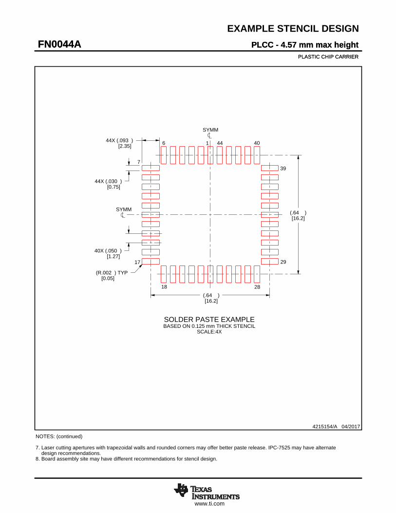
EXAMPLE STENCIL DESIGN
44X (.030 )[0.75]
44X (.093 )[2.35]
(.64 )[16.2]
(.64 )[16.2]
40X (.050 )[1.27]
(R.002 ) TYP[0.05]
PLCC - 4.57 mm max heightFN0044APLASTIC CHIP CARRIER
4215154/A 04/2017
PLCC - 4.57 mm max heightFN0044APLASTIC CHIP CARRIER
NOTES: (continued) 7. Laser cutting apertures with trapezoidal walls and rounded corners may offer better paste release. IPC-7525 may have alternate design recommendations.8. Board assembly site may have different recommendations for stencil design.
SOLDER PASTE EXAMPLEBASED ON 0.125 mm THICK STENCIL
SCALE:4X
SYMM
SYMM
1 446
18 28
29
39
40
7
17

IMPORTANT NOTICE
Texas Instruments Incorporated (TI) reserves the right to make corrections, enhancements, improvements and other changes to itssemiconductor products and services per JESD46, latest issue, and to discontinue any product or service per JESD48, latest issue. Buyersshould obtain the latest relevant information before placing orders and should verify that such information is current and complete.TI’s published terms of sale for semiconductor products (http://www.ti.com/sc/docs/stdterms.htm) apply to the sale of packaged integratedcircuit products that TI has qualified and released to market. Additional terms may apply to the use or sale of other types of TI products andservices.Reproduction of significant portions of TI information in TI data sheets is permissible only if reproduction is without alteration and isaccompanied by all associated warranties, conditions, limitations, and notices. TI is not responsible or liable for such reproduceddocumentation. Information of third parties may be subject to additional restrictions. Resale of TI products or services with statementsdifferent from or beyond the parameters stated by TI for that product or service voids all express and any implied warranties for theassociated TI product or service and is an unfair and deceptive business practice. TI is not responsible or liable for any such statements.Buyers and others who are developing systems that incorporate TI products (collectively, “Designers”) understand and agree that Designersremain responsible for using their independent analysis, evaluation and judgment in designing their applications and that Designers havefull and exclusive responsibility to assure the safety of Designers' applications and compliance of their applications (and of all TI productsused in or for Designers’ applications) with all applicable regulations, laws and other applicable requirements. Designer represents that, withrespect to their applications, Designer has all the necessary expertise to create and implement safeguards that (1) anticipate dangerousconsequences of failures, (2) monitor failures and their consequences, and (3) lessen the likelihood of failures that might cause harm andtake appropriate actions. Designer agrees that prior to using or distributing any applications that include TI products, Designer willthoroughly test such applications and the functionality of such TI products as used in such applications.TI’s provision of technical, application or other design advice, quality characterization, reliability data or other services or information,including, but not limited to, reference designs and materials relating to evaluation modules, (collectively, “TI Resources”) are intended toassist designers who are developing applications that incorporate TI products; by downloading, accessing or using TI Resources in anyway, Designer (individually or, if Designer is acting on behalf of a company, Designer’s company) agrees to use any particular TI Resourcesolely for this purpose and subject to the terms of this Notice.TI’s provision of TI Resources does not expand or otherwise alter TI’s applicable published warranties or warranty disclaimers for TIproducts, and no additional obligations or liabilities arise from TI providing such TI Resources. TI reserves the right to make corrections,enhancements, improvements and other changes to its TI Resources. TI has not conducted any testing other than that specificallydescribed in the published documentation for a particular TI Resource.Designer is authorized to use, copy and modify any individual TI Resource only in connection with the development of applications thatinclude the TI product(s) identified in such TI Resource. NO OTHER LICENSE, EXPRESS OR IMPLIED, BY ESTOPPEL OR OTHERWISETO ANY OTHER TI INTELLECTUAL PROPERTY RIGHT, AND NO LICENSE TO ANY TECHNOLOGY OR INTELLECTUAL PROPERTYRIGHT OF TI OR ANY THIRD PARTY IS GRANTED HEREIN, including but not limited to any patent right, copyright, mask work right, orother intellectual property right relating to any combination, machine, or process in which TI products or services are used. Informationregarding or referencing third-party products or services does not constitute a license to use such products or services, or a warranty orendorsement thereof. Use of TI Resources may require a license from a third party under the patents or other intellectual property of thethird party, or a license from TI under the patents or other intellectual property of TI.TI RESOURCES ARE PROVIDED “AS IS” AND WITH ALL FAULTS. TI DISCLAIMS ALL OTHER WARRANTIES ORREPRESENTATIONS, EXPRESS OR IMPLIED, REGARDING RESOURCES OR USE THEREOF, INCLUDING BUT NOT LIMITED TOACCURACY OR COMPLETENESS, TITLE, ANY EPIDEMIC FAILURE WARRANTY AND ANY IMPLIED WARRANTIES OFMERCHANTABILITY, FITNESS FOR A PARTICULAR PURPOSE, AND NON-INFRINGEMENT OF ANY THIRD PARTY INTELLECTUALPROPERTY RIGHTS. TI SHALL NOT BE LIABLE FOR AND SHALL NOT DEFEND OR INDEMNIFY DESIGNER AGAINST ANY CLAIM,INCLUDING BUT NOT LIMITED TO ANY INFRINGEMENT CLAIM THAT RELATES TO OR IS BASED ON ANY COMBINATION OFPRODUCTS EVEN IF DESCRIBED IN TI RESOURCES OR OTHERWISE. IN NO EVENT SHALL TI BE LIABLE FOR ANY ACTUAL,DIRECT, SPECIAL, COLLATERAL, INDIRECT, PUNITIVE, INCIDENTAL, CONSEQUENTIAL OR EXEMPLARY DAMAGES INCONNECTION WITH OR ARISING OUT OF TI RESOURCES OR USE THEREOF, AND REGARDLESS OF WHETHER TI HAS BEENADVISED OF THE POSSIBILITY OF SUCH DAMAGES.Unless TI has explicitly designated an individual product as meeting the requirements of a particular industry standard (e.g., ISO/TS 16949and ISO 26262), TI is not responsible for any failure to meet such industry standard requirements.Where TI specifically promotes products as facilitating functional safety or as compliant with industry functional safety standards, suchproducts are intended to help enable customers to design and create their own applications that meet applicable functional safety standardsand requirements. Using products in an application does not by itself establish any safety features in the application. Designers mustensure compliance with safety-related requirements and standards applicable to their applications. Designer may not use any TI products inlife-critical medical equipment unless authorized officers of the parties have executed a special contract specifically governing such use.Life-critical medical equipment is medical equipment where failure of such equipment would cause serious bodily injury or death (e.g., lifesupport, pacemakers, defibrillators, heart pumps, neurostimulators, and implantables). Such equipment includes, without limitation, allmedical devices identified by the U.S. Food and Drug Administration as Class III devices and equivalent classifications outside the U.S.TI may expressly designate certain products as completing a particular qualification (e.g., Q100, Military Grade, or Enhanced Product).Designers agree that it has the necessary expertise to select the product with the appropriate qualification designation for their applicationsand that proper product selection is at Designers’ own risk. Designers are solely responsible for compliance with all legal and regulatoryrequirements in connection with such selection.Designer will fully indemnify TI and its representatives against any damages, costs, losses, and/or liabilities arising out of Designer’s non-compliance with the terms and provisions of this Notice.
Mailing Address: Texas Instruments, Post Office Box 655303, Dallas, Texas 75265Copyright © 2017, Texas Instruments Incorporated