mlx90380 - triaxis® resolver
TRANSCRIPT
MLX90380 - Triaxis® Resolver Datasheet
REVISION 11 – 8 JUNE 2021
3901090380
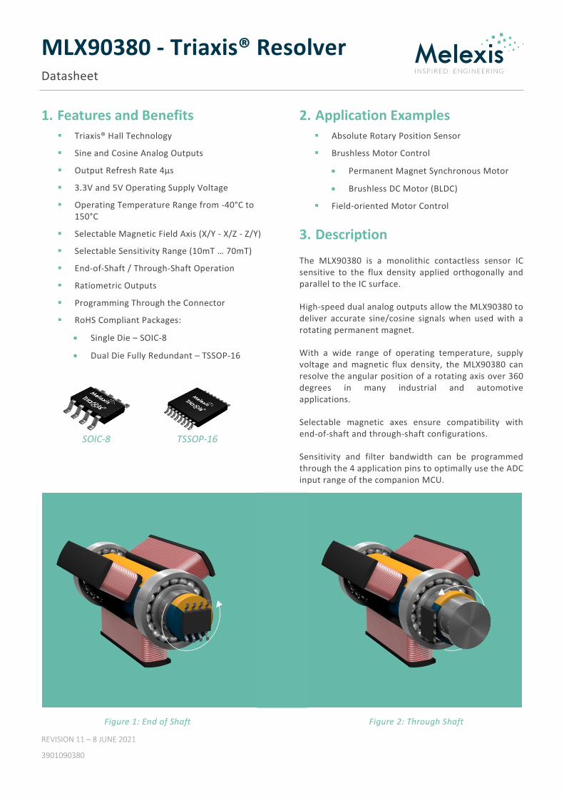
1. Features and Benefits Triaxis® Hall Technology
Sine and Cosine Analog Outputs
Output Refresh Rate 4µs
3.3V and 5V Operating Supply Voltage
Operating Temperature Range from -40°C to 150°C
Selectable Magnetic Field Axis (X/Y - X/Z - Z/Y)
Selectable Sensitivity Range (10mT … 70mT)
End-of-Shaft / Through-Shaft Operation
Ratiometric Outputs
Programming Through the Connector
RoHS Compliant Packages:
• Single Die – SOIC-8
• Dual Die Fully Redundant – TSSOP-16
SOIC-8 TSSOP-16
2. Application Examples Absolute Rotary Position Sensor
Brushless Motor Control
• Permanent Magnet Synchronous Motor
• Brushless DC Motor (BLDC)
Field-oriented Motor Control
3. Description
The MLX90380 is a monolithic contactless sensor IC sensitive to the flux density applied orthogonally and parallel to the IC surface.
High-speed dual analog outputs allow the MLX90380 to deliver accurate sine/cosine signals when used with a rotating permanent magnet.
With a wide range of operating temperature, supply voltage and magnetic flux density, the MLX90380 can resolve the angular position of a rotating axis over 360 degrees in many industrial and automotive applications.
Selectable magnetic axes ensure compatibility with end-of-shaft and through-shaft configurations.
Sensitivity and filter bandwidth can be programmed through the 4 application pins to optimally use the ADC input range of the companion MCU.
Figure 1: End of Shaft Figure 2: Through Shaft
MLX90380 - Triaxis® Resolver Datasheet
Page 2 of 29
REVISION 11 – 23 JUNE 2021
3901090380
Contents 1. Features and Benefits ....................................................................................................................... 1
2. Application Examples ........................................................................................................................ 1
3. Description ....................................................................................................................................... 1
4. Ordering Information ........................................................................................................................ 4
5. Functional Diagram ........................................................................................................................... 7
6. Glossary of Terms ............................................................................................................................. 7
7. Detailed General Description ............................................................................................................ 8
8. Intrinsic Magnetic Axis ...................................................................................................................... 9
8.1. X/Y magnetic axis ........................................................................................................................ 10
8.2. X/Z magnetic axis ........................................................................................................................ 10
8.3. Z/Y magnetic axis ........................................................................................................................ 11
9. Pin Definitions and Descriptions ...................................................................................................... 11
9.1. Pin Definition for SOIC-8 ............................................................................................................. 11
9.2. Pin Definition for TSSOP-16 ......................................................................................................... 12
10. Absolute Maximum Ratings .......................................................................................................... 13
11. General Electrical Specifications .................................................................................................... 13
12. Magnetic Specifications ................................................................................................................ 15
12.1. Sensitivity Temperature Coefficient Characteristic ................................................................... 17
12.2. Output Offset Temperature Drift Characteristic ....................................................................... 17
12.2.1. Output Offset Temperature Drift Characteristic ................................................................. 18
12.2.2. Output Offset Temperature Drift Characteristic vs. Sensitivity ........................................... 19
13. Recommended Application Diagrams ............................................................................................ 20
13.1. MLX90380 in SOIC-8 Package.................................................................................................... 20
13.1.1. Application Diagram VDD3V3 .............................................................................................. 20
13.1.2. Application Diagram VDD5V ................................................................................................ 20
13.2. MLX90380 in TSSOP-16 Package ............................................................................................... 21
13.2.1. Application Diagram VDD3V3 .............................................................................................. 21
13.2.2. Application Diagram VDD5V ................................................................................................ 22
14. Package Information ..................................................................................................................... 23
14.1. SOIC-8 Package Dimensions ...................................................................................................... 23
14.2. SOIC-8 Pin out and Marking ...................................................................................................... 23
14.3. SOIC-8 IMC Positioning ............................................................................................................. 24

MLX90380 - Triaxis® Resolver Datasheet
Page 3 of 29
REVISION 11 – 23 JUNE 2021
3901090380
14.4. TSSOP-16 Package Dimensions ................................................................................................. 25
14.5. TSSOP-16 Pin out and Marking ................................................................................................. 26
14.6. TSSOP-16 IMC positioning ......................................................................................................... 26
15. Standard Information .................................................................................................................... 28
16. ESD Precautions ............................................................................................................................ 28
17. Contact ......................................................................................................................................... 29
18. Disclaimer ..................................................................................................................................... 29
MLX90380 - Triaxis® Resolver Datasheet
Page 4 of 29
REVISION 11 – 23 JUNE 2021
3901090380
4. Ordering Information (1)
Product Ordering Code Temperature Package Option Code Packing Form
MLX90380LDC-BAA-000-RE -40°C to 150°C SOIC-8 BAA-000 Reel
MLX90380LDC-BAA-100-RE -40°C to 150°C SOIC-8 BAA-100 Reel
MLX90380LDC-BAA-500-RE -40°C to 150°C SOIC-8 BAA-500 Reel
MLX90380LDC-BAB-000-RE -40°C to 150°C SOIC-8 BAB-000 Reel
MLX90380LDC-BAB-003-RE -40°C to 150°C SOIC-8 BAB-003 Reel
MLX90380LDC-BAB-005-RE -40°C to 150°C SOIC-8 BAB-005 Reel
MLX90380LDC-BAB-010-RE -40°C to 150°C SOIC-8 BAB-010 Reel
MLX90380LDC-BAB-023-RE -40°C to 150°C SOIC-8 BAB-023 Reel
MLX90380LDC-BAB-025-RE -40°C to 150°C SOIC-8 BAB-025 Reel
MLX90380LDC-BAB-043-RE -40°C to 150°C SOIC-8 BAB-043 Reel
MLX90380LDC-BAB-045-RE -40°C to 150°C SOIC-8 BAB-045 Reel
MLX90380LDC-BAB-100-RE -40°C to 150°C SOIC-8 BAB-100 Reel
MLX90380LDC-BAB-103-RE -40°C to 150°C SOIC-8 BAB-103 Reel
MLX90380LDC-BAB-105-RE -40°C to 150°C SOIC-8 BAB-105 Reel
MLX90380LDC-BAB-120-RE -40°C to 150°C SOIC-8 BAB-120 Reel
MLX90380LDC-BAB-123-RE -40°C to 150°C SOIC-8 BAB-123 Reel
MLX90380LDC-BAB-125-RE -40°C to 150°C SOIC-8 BAB-125 Reel
MLX90380LDC-BAB-140-RE -40°C to 150°C SOIC-8 BAB-140 Reel
MLX90380LDC-BAB-143-RE -40°C to 150°C SOIC-8 BAB-143 Reel
MLX90380LDC-BAB-145-RE -40°C to 150°C SOIC-8 BAB-145 Reel
MLX90380LDC-BAB-200-RE -40°C to 150°C SOIC-8 BAB-200 Reel
MLX90380LDC-BAB-305-RE -40°C to 150°C SOIC-8 BAB-305 Reel
MLX90380LDC-BAB-403-RE -40°C to 150°C SOIC-8 BAB-403 Reel
MLX90380LDC-BAB-506-RE -40°C to 150°C SOIC-8 BAB-506 Reel
MLX90380LDC-BAB-543-RE -40°C to 150°C SOIC-8 BAB-543 Reel
MLX90380LDC-BAC-000-RE -40°C to 150°C SOIC-8 BAC-000 Reel
1 Other option codes and packing forms are available upon request. Every combination in Table 2 can be made pending on yearly volume. Please contact your sales representative to see what combinations are available.

MLX90380 - Triaxis® Resolver Datasheet
Page 5 of 29
REVISION 11 – 23 JUNE 2021
3901090380
Product Ordering Code Temperature Package Option Code Packing Form
MLX90380LDC-BAC-100-RE -40°C to 150°C SOIC-8 BAC-100 Reel
MLX90380LDC-BAC-125-RE -40°C to 150°C SOIC-8 BAC-125 Reel
MLX90380LDC-BAC-524-RE -40°C to 150°C SOIC-8 BAC-524 Reel
MLX90380LDC-BAC-545-RE -40°C to 150°C SOIC-8 BAC-545 Reel
MLX90380LGO-BAA-000-RE -40°C to 150°C TSSOP-16 BAA-000 Reel
MLX90380LGO-BAA-100-RE -40°C to 150°C TSSOP-16 BAA-100 Reel
MLX90380LGO-BAB-003-RE -40°C to 150°C TSSOP-16 BAB-003 Reel
MLX90380LGO-BAB-005-RE -40°C to 150°C TSSOP-16 BAB-005 Reel
MLX90380LGO-BAB-015-RE -40°C to 150°C TSSOP-16 BAB-015 Reel
MLX90380LGO-BAB-023-RE -40°C to 150°C TSSOP-16 BAB-023 Reel
MLX90380LGO-BAB-025-RE -40°C to 150°C TSSOP-16 BAB-025 Reel
MLX90380LGO-BAB-043-RE -40°C to 150°C TSSOP-16 BAB-043 Reel
MLX90380LGO-BAB-045-RE -40°C to 150°C TSSOP-16 BAB-045 Reel
MLX90380LGO-BAB-100-RE -40°C to 150°C TSSOP-16 BAB-100 Reel
MLX90380LGO-BAB-103-RE -40°C to 150°C TSSOP-16 BAB-103 Reel
MLX90380LGO-BAB-105-RE -40°C to 150°C TSSOP-16 BAB-105 Reel
MLX90380LGO-BAB-123-RE -40°C to 150°C TSSOP-16 BAB-123 Reel
MLX90380LGO-BAB-125-RE -40°C to 150°C TSSOP-16 BAB-125 Reel
MLX90380LGO-BAB-143-RE -40°C to 150°C TSSOP-16 BAB-143 Reel
MLX90380LGO-BAB-145-RE -40°C to 150°C TSSOP-16 BAB-145 Reel
MLX90380LGO-BAB-400-RE -40°C to 150°C TSSOP-16 BAB-400 Reel
MLX90380LGO-BAC-000-RE -40°C to 150°C TSSOP-16 BAC-000 Reel
MLX90380LGO-BAC-100-RE -40°C to 150°C TSSOP-16 BAC-100 Reel
Table 1: Ordering Codes available. All option codes of Table 2 can be made.
Packing delivery form
Package codeTemperature codeProduct name
Option code for variant

MLX90380 - Triaxis® Resolver Datasheet
Page 6 of 29
REVISION 11 – 23 JUNE 2021
3901090380
Legend:
Temperature Code: L: from -40°C to 150°C
Package Code: DC: for SOIC-8 package
GO: for TSSOP-16 package (dual die)
Option Code:
BAx-123
Sensitivity Temperature Coefficient:
BAA-xxx: SmCo magnet BAB-xxx: NdFeB magnet BAC-xxx: Ferrite magnet
Sensitivity:
BAx-xx0: 40mT magnetic range(2)
BAx-xx1: 10mT magnetic range(2) for 3.3V operating supply voltage only
BAx-xx2: 20mT magnetic range(2)
BAx-xx3: 30mT magnetic range(2)
BAx-xx4: 50mT magnetic range(2)
BAx-xx5: 60mT magnetic range(2)
BAx-xx6: 70mT magnetic range(2) BAx-xx7: 15mT magnetic range(2) for 5V operating supply voltage only
Magnetic axis:
BAx-x0x: X/Y magnetic axis – equal sensitivity(3)
BAx-x1x: X/Z magnetic axis – equal sensitivity(3)
BAx-x2x: Z/Y magnetic axis – equal sensitivity(3)
BAx-x3x: X/Z magnetic axis – sensitivity mismatch(4)
BAx-x4x: Z/Y magnetic axis – sensitivity mismatch(4)
Operating voltage and Bandwidth:
BAx-0xx: 3.3V operating supply voltage – low BW BAx-1xx: 5V operating supply voltage – low BW BAx-2xx: 3.3V operating supply voltage – medium BW BAx-3xx: 5V operating supply voltage – medium BW BAx-4xx: 3.3V operating supply voltage – high BW BAx-5xx: 5V operating supply voltage – high BW
Packing Form: RE: for Reel
Ordering Example: MLX90380LDC-BAA-000-RE: SOIC-8 150, SmCo magnet, 3.3V operating supply voltage, Low bandwidth, X/Y magnetic axis, 40mT full scale magnetic range, Reel
Table 2: Order code Description
2 The magnetic range is the in-plane (X or Y) flux density, that results in a ±40%VDD output swing with a VOQ of 50%VDD with TA=25°C, VDD=VDDNOM 3 Magnetic axis for: two pole magnet end of shaft / on axis and multi-pole magnet off-axis / through-shaft application. 4 Magnetic axis for: two pole magnet off-axis / through-shaft application. The magnetic flux norm for the Z axis is double the magnetic flux norm for the X or Y axis: Bxy/Bz = 50%.

MLX90380 - Triaxis® Resolver Datasheet
Page 7 of 29
REVISION 11 – 23 JUNE 2021
3901090380
5. Functional Diagram
Figure 3: Functional Diagram
6. Glossary of Terms Gauss (G), Tesla (T) Units for the magnetic flux density − 1 mT = 10 G TC Temperature Coefficient (in ppm/°C.)
NC Not Connected
EMC Electro-Magnetic Compatibility Table 3: Glossary of Terms
MLX90380 - Triaxis® Resolver Datasheet
Page 8 of 29
REVISION 11 – 23 JUNE 2021
3901090380
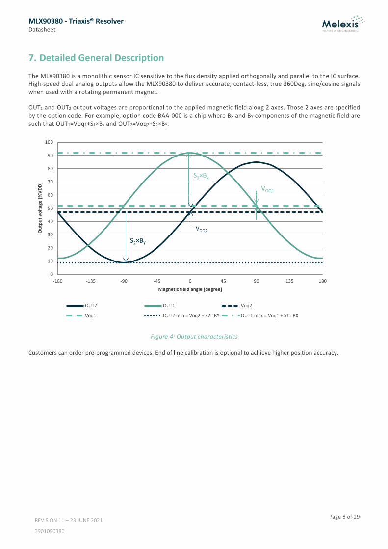
7. Detailed General Description
The MLX90380 is a monolithic sensor IC sensitive to the flux density applied orthogonally and parallel to the IC surface. High-speed dual analog outputs allow the MLX90380 to deliver accurate, contact-less, true 360Deg. sine/cosine signals when used with a rotating permanent magnet.
OUT1 and OUT2 output voltages are proportional to the applied magnetic field along 2 axes. Those 2 axes are specified by the option code. For example, option code BAA-000 is a chip where BX and BY components of the magnetic field are such that OUT1=Voq1+S1×Bx and OUT2=Voq2+S2×BY.
Figure 4: Output characteristics Customers can order pre-programmed devices. End of line calibration is optional to achieve higher position accuracy.
0
10
20
30
40
50
60
70
80
90
100
-180 -135 -90 -45 0 45 90 135 180
Out
put v
olta
ge [%
VDD]
Magnetic field angle [degree]
OUT2 OUT1 Voq2
Voq1 OUT2 min = Voq2 + S2 . BY OUT1 max = Voq1 + S1 . BX
S1×Bx
S2×BY
VOQ2
VOQ1

MLX90380 - Triaxis® Resolver Datasheet
Page 9 of 29
REVISION 11 – 23 JUNE 2021
3901090380
8. Intrinsic Magnetic Axis
Figure 5: Axis configuration
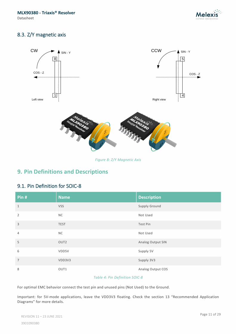
Figure 5 gives the axis convention. Thus, take for example an IC in Z/Y configuration. Then, OUT1 will give Bz & OUT2 will give By.
The following sections list a detailed explanation of the intrinsic axis. It explains clock wise and counter clock wise behavior of the angle calculation.
CW – Clockwise turn: The magnet needs to turn in the CW direction to get a positive slope of the angle calculated by ATAN.
CCW – Counterclockwise turn: The magnet needs to turn in the CCW direction to get a positive slope of the angle calculated by ATAN.
The CW - CCW rotation direction can be modified by changing the COS / SIN assignment to SIN / COS with an angle correction of 90 Deg.
=
COSSINATANα
The convention of preprogrammed parts is such that OUT2 is seen as SIN and OUT1 as COS.

MLX90380 - Triaxis® Resolver Datasheet
Page 10 of 29
REVISION 11 – 23 JUNE 2021
3901090380
8.1. X/Y magnetic axis
CW
Vss
NC
Vdd
Out
1
1
NC
Vdd
TEST
Out
2
8
4
5
COS - X
SIN - Y
Top view
Figure 6: X/Y Magnetic Axis
8.2. X/Z magnetic axis
CCWCW
8 5
SIN - Z
COS - X
1 4
SIN - Z
COS - X
Top view Bottom view
Figure 7: X/Z Magnetic Axis
MLX90380 - Triaxis® Resolver Datasheet
Page 11 of 29
REVISION 11 – 23 JUNE 2021
3901090380
8.3. Z/Y magnetic axis
CW CCW
4
5
SIN - Y
COS - Z
8
1
SIN - Y
COS - Z
Left view Right view
Figure 8: Z/Y Magnetic Axis
9. Pin Definitions and Descriptions
9.1. Pin Definition for SOIC-8
Pin # Name Description
1 VSS Supply Ground
2 NC Not Used
3 TEST Test Pin
4 NC Not Used
5 OUT2 Analog Output SIN
6 VDD5V Supply 5V
7 VDD3V3 Supply 3V3
8 OUT1 Analog Output COS
Table 4: Pin Definition SOIC-8
For optimal EMC behavior connect the test pin and unused pins (Not Used) to the Ground.
Important: for 5V-mode applications, leave the VDD3V3 floating. Check the section 13 “Recommended Application Diagrams” for more details.
MLX90380 - Triaxis® Resolver Datasheet
Page 12 of 29
REVISION 11 – 23 JUNE 2021
3901090380
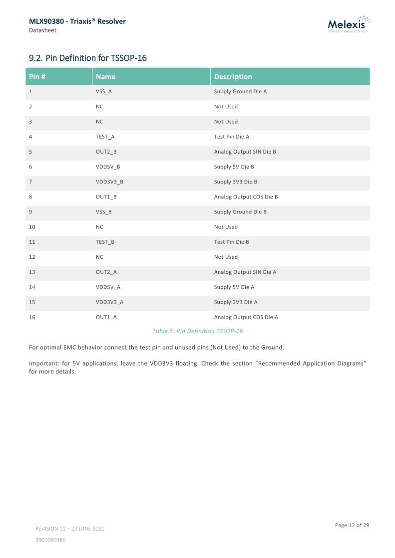
9.2. Pin Definition for TSSOP-16
Pin # Name Description
1 VSS_A Supply Ground Die A
2 NC Not Used
3 NC Not Used
4 TEST_A Test Pin Die A
5 OUT2_B Analog Output SIN Die B
6 VDD5V_B Supply 5V Die B
7 VDD3V3_B Supply 3V3 Die B
8 OUT1_B Analog Output COS Die B
9 VSS_B Supply Ground Die B
10 NC Not Used
11 TEST_B Test Pin Die B
12 NC Not Used
13 OUT2_A Analog Output SIN Die A
14 VDD5V_A Supply 5V Die A
15 VDD3V3_A Supply 3V3 Die A
16 OUT1_A Analog Output COS Die A
Table 5: Pin Definition TSSOP-16
For optimal EMC behavior connect the test pin and unused pins (Not Used) to the Ground.
Important: for 5V applications, leave the VDD3V3 floating. Check the section “Recommended Application Diagrams” for more details.

MLX90380 - Triaxis® Resolver Datasheet
Page 13 of 29
REVISION 11 – 23 JUNE 2021
3901090380
10. Absolute Maximum Ratings
Parameter Symbol Min. Max. Unit Condition
Supply Voltage (5V) VDD5V -16 24 V
Supply Voltage (3.3V) VDD3V3 -0.3 7 V
Supply Current(5) IDD -10 10 mA Excluding external load on OUT1&2.
Negative Output Voltage VOUT -0.3 - V
Positive Output Voltage (5V Application Diagram)
VOUT - 18 V
Positive Output Voltage (3.3V Application Diagram)
VOUT - 17 V
Output Current IOUT -20 20 mA
Operating Temperature Range TA -40 150 °C
Maximum Junction Temperature TJ - 165 °C
Storage Temperature Range TS -55 165 °C
ESD Sensitivity (Human Body Model) AEC-Q100-002 standard
ESDHBM - 2 kV Valid for SOIC-8. TSSOP-16 cross die ESD limit is 1.5kV.
ESD Sensitivity (Charged Device Model) AEC-Q100-011 standard
ESDCDM - 500 V
Maximum Flux Density B -1 1 T
Table 6: Absolute Maximum Ratings
Exceeding the absolute maximum ratings may cause permanent damage. Exposure to absolute maximum-rated conditions for extended periods may affect device reliability.
11. General Electrical Specifications
Operating Characteristics, VDD=3.135V to 3.6V or VDD=4.5V to 5.5V (depending on the option code), TA = -40°C to 150°C (unless otherwise specified)
Electrical Parameter Symbol Min. Typ. Max. Unit Condition
Supply Voltage (operating) VDD3V3 3.135 3.3 3.6 V SOIC-8 and TSSOP-16 packages
Supply Voltage (operating) VDD5V 4.5 5 5.5 V SOIC-8 and TSSOP-16 packages
Supply Current IDD
5 6
- -
9
10
mA mA
Excluding external load on OUT1&2 3.135 ≤ VDD ≤ 3.6 4.5 ≤ VDD ≤ 5.5
5 Note IDD may exceed 10mA with a pull-down on OUT1&2.

MLX90380 - Triaxis® Resolver Datasheet
Page 14 of 29
REVISION 11 – 23 JUNE 2021
3901090380
Electrical Parameter Symbol Min. Typ. Max. Unit Condition
Power On Reset Voltage Rising VPOR_H
2.4 2.9
2.75 3.4
3
3.9
V V
OUT HiZ operating mode Application Diagram VDD3V3 Application Diagram VDD5V
Power On Reset Voltage Falling VPOR_L
2.1 2.5
2.4
3.05
2.7 3.5
V V
Operating mode OUT HiZ Application Diagram VDD3V3 Application Diagram VDD5V
Programming Voltage (PTC) MT7V 6.1 6.5 7 V Rising Entry Level on VDD
Load Current Range IOUT -1 - 1 mA
Load Resistance Range( 6) RL
10 5
- -
∞ ∞
kΩ kΩ
Connected between OUT and GND Application Diagram VDD3V3 Application Diagram VDD5V
Load Capacitor Range CL 1.5 2.2 10 ηF Connected between OUT and GND
Output Voltage Range VO 5
10 - -
95 90
%VDD %VDD
Linearity better than 1.5% Linearity better than 0.5%
Output Resistance ROUT - 25 - Ω IOUT= ±1mA
Power-On Time(7) tON - - 200 µs High bandwidth programming VPOR_H ≤ VDD ≤ VDD5V_Max
VPOR_H ≤ VDD ≤ VDD3V3_Max
Chopping Frequency FCHOP 0.9 1 1.1 MHz
Output Update Period TS - 4 - µs Each field component takes 2µs, measured sequentially
Output Noise Voltage(8) Vnrms
- - -
- - -
3.1 4.6 10
mV mV mV
RMS noise, B=0mT, VDD = typical value S=1 %VDD/mT (50mV/mT at VDD=5V) Low bandwidth programming Medium bandwidth programming High bandwidth programming
Nyquist Frequency Fnyq - 125 - kHz
Tracking Delay(9) - - -
12 29.5 74
17.5 38
85.5
µs µs µs
High bandwidth Medium bandwidth Low bandwidth
Table 7 General Electrical Specifications
6 A Pull down enables EEPROM error detection when the output goes in HiZ mode. 7 Lower bandwidth programming increases the Power-On Time by the tracking delay (see footnote 9). 8 Higher sensitivity programming may increase the output noise voltage. 9 Tracking Delay is defined as the time delay between a rotating magnetic stimuli and the change on both outputs, SIN and COS. This delay includes the sample and hold filter which can be programmed by the customer according to the following equation: Vo=Vi/n + nz-1 Vo/n with Bandwidth=1/(2πnTs) and n=1, 2, …, 16.

MLX90380 - Triaxis® Resolver Datasheet
Page 15 of 29
REVISION 11 – 23 JUNE 2021
3901090380
12. Magnetic Specifications (10)
Operating Characteristics, VDD=3.135V to 3.6V or VDD=4.5V to 5.5V (depending on the option code), TA = -40°C to 150°C (unless otherwise specified).
Magnetic Parameter Symbol Min. Typ. Max. Unit Condition
Full Scale Magnetic Range (programmable)
Bfs 10 - 70 mT
Magnetic Flux Density Bz - - 140 mT
Sensitivity(11) S
- - - - - - - -
1(12)
4(12)
2(12)
1.33(12)
0.8(12)
0.66(12)
0.57(12) 2.66(12)
- - - - - - - -
%VDD/mT %VDD/mT %VDD/mT %VDD/mT %VDD/mT %VDD/mT %VDD/mT %VDD/mT
xx0: 40mT magnetic range xx1: 10mT magnetic range( 13) xx2: 20mT magnetic range xx3: 30mT magnetic range xx4: 50mT magnetic range xx5: 60mT magnetic range xx6: 70mT magnetic range xx7: 15mT magnetic range( 14)
Sensitivity Accuracy -5 -8
- -
5 8
% %
X/Y magnetic axis Z magnetic axis TA=25°C, VDD=VDDNOM, S=1%VDD/mT
Sensitivity Temperature Coefficient(15)
TCS
- - -
350
1100 2000
- - -
ppm/°C ppm/°C ppm/°C
First Order approximation SmCo NdFeB Ferrite
Sensitivity Temperature Coefficient Drift
TCSdrift -500 - 500 ppm/°C Temperature drift around programmed TCS
Sensitivity Ratiometry -2.5 - 2.5 % / V
Linearity
-0.5 -0.5 -1.5 -1.5
- - - -
0.5 0.5 1.5 1.5
% % % %
VDD=5V, output voltage within [0.5V;4.5V] VDD=3.3V, output voltage within [0.33V;2.97V] VDD=5V, output voltage within [0.25V;4.75V] VDD=3.3V, output voltage in [0.165V;3.135V]
Sensitivity Mismatch -5 -
-5
- -20
-
5 - 5
% % %
X vs. Y, with/without gain adjustment Z vs. X, Z vs. Y, without gain adjustment Z vs. X, Z vs. Y, with gain adjustment
10 Please refer to the User_Interface_description_MLX90380_PSF_sample.xls.pdf for customer programmable parameters. 11 Sensitivity and associated magnetic full scale range are factory programmed (see Option Codes). 12 For option code x3x and x4x the sensitivity for the Z axis is half of the sensitivity for the X or Y axis. The given figure is for the X or Y axis. 13 for 3.3V operating supply voltage only 14 for 5V operating supply voltage only 15 See section 12.1 for second order behavior.
MLX90380 - Triaxis® Resolver Datasheet
Page 16 of 29
REVISION 11 – 23 JUNE 2021
3901090380
Magnetic Parameter Symbol Min. Typ. Max. Unit Condition
Output Offset Level VOQ 47.5 50 52.5 %VDD B=0mT, TA=25°C
Output Offset Temperature Drift(16)
-1.5 -2.2
0 0
1.5 2.2
%VDD %VDD
VDD=5V VDD=3.3V B=0mT, S=1 %VDD/mT
Output Offset Ratiometry -2.5 - 2.5 % B=0mT (dVOQ / VOQ) - (dVDD / VDD) -10% < dVDD/VDD < 10%
Magnetic Angular Speed 0 - 25000 rpm
Signal Phase Shift PHI - 1.8 - Degree At 25000 rpm, high bandwidth programming
Output Update Rate - 1.6 - Sample/ Degree
At 25000 rpm, high bandwidth programming
Total Angular Error without Correction(17)
-10 -15
- 10 15
Degree Degree
T=25°C -40°C ≤ T ≤ 150°C
Total Angular Error with Dynamic Compensation(18)
-1 - 1 Degree
Table 8: Magnetic Specifications
16 See section 12.2 for the full Output Offset Temperature Drift Characteristics 17 Total angle error with an external homogeneous magnetic field stimulus. System design and manufacturing (magnet eccentricity and off-axis) may degrade the accuracy. 18 This system error budget is explained in more detail in a separate application note. It is dependent on the magnetic system and the correction algorithm of the ECU. A very popular method to reduce total angle error is offset and amplitude correction (e.g. min/max COS/SIN scaling by the system ECU after one full magnet revolution). The total angle error refers only to the linearity error associated to the MLX90380. The linearity error associated to the magnetic and mechanical (off-axis, eccentricity) design is not included and should be considered as an additional contribution. The total error can be reduced either statically (room temperature compensation) or dynamically (continuous compensation) through the off-chip signal processing performing the angular computation i.e. arctan(OUT2/OUT1). The compensation is applied prior to computing the arctangent function: offset, gain and phase correction can be applied.

MLX90380 - Triaxis® Resolver Datasheet
Page 17 of 29
REVISION 11 – 23 JUNE 2021
3901090380
12.1. Sensitivity Temperature Coefficient Characteristic
The sensitivity temperature coefficient of the MLX90380 is a first order sensitivity compensation to counter the degrading of the magnets field strength over temperature. The TCS is foreseen with a target TCS of SmCo, NdFeB and Ferrite. The actual TCS of the sensor will show a small 2nd order on the target as illustrated in the figure below.
Figure 9: Target TCS vs. 2nd order TCS
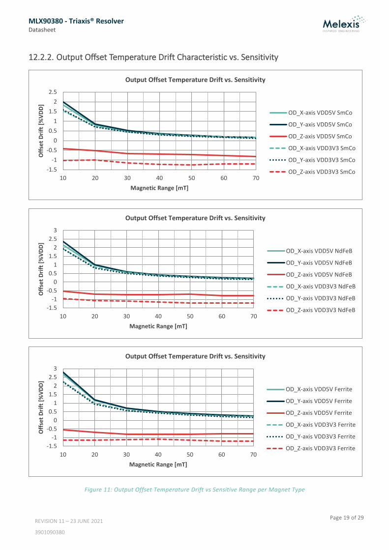
12.2. Output Offset Temperature Drift Characteristic
In the Magnetic Specifications, the Output Offset Temperature Drift of the MLX90380 is specified for B=0mT, VDD=VDDNOM, S=1 %VDD/mT -40°C ≤ T ≤ 150°C. The charts below list the Output Offset Temperature Drift characteristics for the full magnetic range.
0
150
300
450
600
750
900
1050
1200
1350
1500
1650
1800
1950
2100
2250
-40 -30 -20 -10 0 10 20 30 40 50 60 70 80 90 100 110 120 130 140 150
TCS
[ppn
/°C]
Temperature [°C]
Sensitivity Temperature Coefficient
Target TCS Ferrite
TCS Ferrite
Target TCS NdFeB
TCS NdFeB
Target TCS SmCo
TCS SmCo

MLX90380 - Triaxis® Resolver Datasheet
Page 18 of 29
REVISION 11 – 23 JUNE 2021
3901090380
12.2.1. Output Offset Temperature Drift Characteristic
Figure 10: Output Offset Temperature Drift per Magnet Type
-1.4-1.2
-1-0.8-0.6-0.4-0.2
00.20.40.6
-40 -20 0 20 40 60 80 100 120 140
Offs
et D
rift [
%VD
D]
Temperature [°C]
Output Offset Temperature Drift with programmed S = 1 %VDD/mT
OD_X-axis VDD5V SmCo
OD_Y-axis VDD5V SmCo
OD_Z-axis VDD5V SmCo
OD_X-axis VDD3V3 SmCo
OD_Y-axis VDD3V3 SmCo
OD_Z-axis VDD3V3 SmCo
-1.4-1.2
-1-0.8-0.6-0.4-0.2
00.20.40.6
-40 -20 0 20 40 60 80 100 120 140
Offs
et D
rift [
%VD
D]
Temperature [°C]
Output Offset Temperature Drift with programmed S = 1 %VDD/mT
OD_X-axis VDD5V NdFeB
OD_Y-axis VDD5V NdFeB
OD_Z-axis VDD5V NdFeB
OD_X-axis VDD3V3 NdFeB
OD_Y-axis VDD3V3 NdFeB
OD_Z-axis VDD3V3 NdFeB
-1.2-1
-0.8-0.6-0.4-0.2
00.20.40.6
-40 -20 0 20 40 60 80 100 120 140
Offs
et D
rift [
%VD
D]
Temperature [°C]
Output Offset Temperature Drift with programmed S = 1 %VDD/mT
OD_X-axis VDD5V Ferrite
OD_Y-axis VDD5V Ferrite
OD_Z-axis VDD5V Ferrite
OD_X-axis VDD3V3 Ferrite
OD_Y-axis VDD3V3 Ferrite
OD_Z-axis VDD3V3 Ferrite
MLX90380 - Triaxis® Resolver Datasheet
Page 19 of 29
REVISION 11 – 23 JUNE 2021
3901090380
12.2.2. Output Offset Temperature Drift Characteristic vs. Sensitivity
Figure 11: Output Offset Temperature Drift vs Sensitive Range per Magnet Type
-1.5-1
-0.50
0.51
1.52
2.5
10 20 30 40 50 60 70
Offs
et D
rift [
%VD
D]
Magnetic Range [mT]
Output Offset Temperature Drift vs. Sensitivity
OD_X-axis VDD5V SmCo
OD_Y-axis VDD5V SmCo
OD_Z-axis VDD5V SmCo
OD_X-axis VDD3V3 SmCo
OD_Y-axis VDD3V3 SmCo
OD_Z-axis VDD3V3 SmCo
-1.5-1
-0.50
0.51
1.52
2.53
10 20 30 40 50 60 70
Offs
et D
rift [
%VD
D]
Magnetic Range [mT]
Output Offset Temperature Drift vs. Sensitivity
OD_X-axis VDD5V NdFeB
OD_Y-axis VDD5V NdFeB
OD_Z-axis VDD5V NdFeB
OD_X-axis VDD3V3 NdFeB
OD_Y-axis VDD3V3 NdFeB
OD_Z-axis VDD3V3 NdFeB
-1.5-1
-0.50
0.51
1.52
2.53
10 20 30 40 50 60 70
Offs
et D
rift [
%VD
D]
Magnetic Range [mT]
Output Offset Temperature Drift vs. Sensitivity
OD_X-axis VDD5V Ferrite
OD_Y-axis VDD5V Ferrite
OD_Z-axis VDD5V Ferrite
OD_X-axis VDD3V3 Ferrite
OD_Y-axis VDD3V3 Ferrite
OD_Z-axis VDD3V3 Ferrite

MLX90380 - Triaxis® Resolver Datasheet
Page 20 of 29
REVISION 11 – 23 JUNE 2021
3901090380
13. Recommended Application Diagrams
13.1. MLX90380 in SOIC-8 Package
13.1.1. Application Diagram VDD3V3
C22.2nF
MLX90380Vss
NC
Vdd5V
Out1
1
NC Vdd3V3
TEST
Out2
8
4 5
C1100nF
C32.2nF
VDD3V3
GND
OUT 2
3V3
AD
C / M
CU
OUT 1
Figure 12: Application Diagram VDD3V3
13.1.2. Application Diagram VDD5V
C22.2nF
MLX90380Vss
NC
Vdd5V
Out1
1
NC Vdd3V3
TEST
Out2
8
4 5
C1100nF
C32.2nF
VDD5V
GND
OUT 2
5V
AD
C / M
CU
OUT 1
Figure 13: Application Diagram VDD5V
MLX90380 - Triaxis® Resolver Datasheet
Page 21 of 29
REVISION 11 – 23 JUNE 2021
3901090380
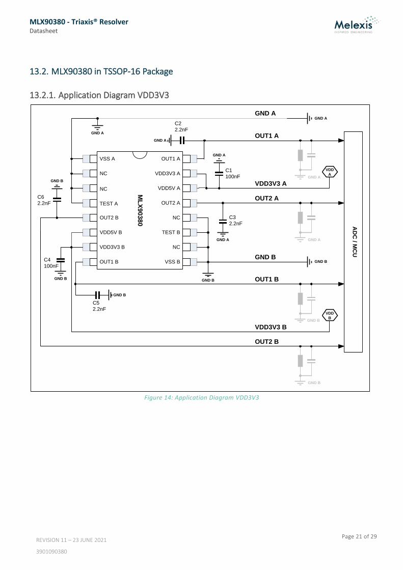
13.2. MLX90380 in TSSOP-16 Package
13.2.1. Application Diagram VDD3V3
GND AGND A
OUT1 A
AD
C / M
CU
MLX90380
VSS A
VSS B
VDD3V3 B
VDD3V3 A
OUT1 A
OUT1 B
TEST A
NC
TEST B
OUT2 B
OUT2 A
VDD5V A
VDD5V B
NC
NC
NC
C52.2nF
C4100nF
C62.2nF
C22.2nF
C1100nF
C32.2nF
VDDA
VDD3V3 AGND A
OUT2 A
GND A
GND BGND B
OUT1 B
VDD B
VDD3V3 BGND B
OUT2 B
GND B
GND A
GND A
GND A
GND A
GND B
GND B
GND B
GND B
Figure 14: Application Diagram VDD3V3

MLX90380 - Triaxis® Resolver Datasheet
Page 22 of 29
REVISION 11 – 23 JUNE 2021
3901090380
13.2.2. Application Diagram VDD5V
GND AGND A
OUT1 A
AD
C / M
CU
MLX90380
VSS A
VSS B
VDD3V3 B
VDD3V3 A
OUT1 A
OUT1 B
TEST A
NC
TEST B
OUT2 B
OUT2 A
VDD5V A
VDD5V B
NC
NC
NC
C52.2nF
C4100nF
C62.2nF
C22.2nF
C1100nF
C32.2nF
VDDA
VDD5V AGND A
OUT2 A
GND A
GND BGND B
OUT1 B
VDD B
VDD5V BGND B
OUT2 B
GND B
GND A
GND A
GND A
GND A
GND B
GND B
GND B
GND B
Figure 15: Application Diagram VDD5V

MLX90380 - Triaxis® Resolver Datasheet
Page 23 of 29
REVISION 11 – 23 JUNE 2021
3901090380
14. Package Information
14.1. SOIC-8 Package Dimensions
Figure 16: SOIC-8 Package Dimensions
14.2. SOIC-8 Pin out and Marking
Figure 17: SOIC-8 Pin out and Marking
0.190.25
NOTES:
All dimensions are in millimeters (angles in degrees).* Dimension does not include mold flash, protrusions or gate burrs (shall not exceed 0.15 per side).** Dimension does not include interleads flash or protrusion (shall not exceed 0.25 per side).*** Dimension does not include dambar protrusion. Allowable dambar protrusion shall be 0.08 mm total in excess of the dimension at maximum material condition. Dambar cannot be located on the lower radius of the foot.
5.806.20
1.27 TYP
4.804.98*
1.521.72
0.1000.250
1.371.57
0.360.46***
3.813.99**
0°8°
0.411.27
Marking :
Part Number MLX90380 (3 digits)
380Die Version (2 digits)
12345
Week Date code (2 digits)Year Date code (2 digits)
YY WW
Bx
1
8
4
5
380BxF12345
Xy
TestVS
S
OU
T2
VDD5
V
VDD3
V3
OU
T1
Top
Bottom
Xy
Lot number (5 digits)
Split lot number
FFab Identifier (1 letter)

MLX90380 - Triaxis® Resolver Datasheet
Page 24 of 29
REVISION 11 – 23 JUNE 2021
3901090380
14.3. SOIC-8 IMC Positioning
0.46 +/- 0.06
1
8
4
5
COS - X
SIN - YCW
1.16 +/- 0.155
Die rotation tolerance ±2°
2.089+/- 0.15
1.95
5+/
- 0.2
Figure 18: SOIC-8 IMC positioning
Figure 19: Angular detection MLX90380 SOIC-8
1 2 3 4
8 7 6 5
~ 0 Deg.*
1 2 3 4
8 7 6 5
~ 90 Deg.*
1 2 3 4
8 7 6 5
~ 270 Deg.*
1 2 3 4
8 7 6 5
N
~ 180 Deg.*
* No absolute reference for the angular information.
NS
N
S
N S
N
S
Angle detection MLX90380 SOIC-8

MLX90380 - Triaxis® Resolver Datasheet
Page 25 of 29
REVISION 11 – 23 JUNE 2021
3901090380
14.4. TSSOP-16 Package Dimensions
Figure 20: TSSOP-16 Package Dimensions
0.090.20
1.0 DIAREF
NOTES:
All dimensions are in millimeters (angles in degrees).* Dimension does not include mold flash, protrusions or gate burrs (shall not exceed 0.15 per side).** Dimension does not include interleads flash or protrusion (shall not exceed 0.25 per side).*** Dimension does not include dambar protrusion. Allowable dambar protrusion shall be 0.08 mm total in excess of the dimension at maximum material condition. Dambar cannot be located on the lower radius of the foot.REF: Reference dimensions as stated in packaging supplier POD, based on JEDEC.
0.20 ± 0.04
12O REF
0.09 MIN
0.09 MIN
0.500.75
1.0 ± 0.2
12O REF
0O 8O
6.4 ± 0.24.304.50**
0.65 ± 0.04
1.0 REF
1.0REF
4.905.10*
1.1 MAX
0.050.15
0.850.95
0.190.30***

MLX90380 - Triaxis® Resolver Datasheet
Page 26 of 29
REVISION 11 – 23 JUNE 2021
3901090380
14.5. TSSOP-16 Pin out and Marking
Figure 21: TSSOP-16 Pin out and Marking
14.6. TSSOP-16 IMC positioning
1 8
916
COS
SIN
Die A Die BCOS
SIN
1.95
2.45
1.171.37
3.403.60
CW
CW
0.30 +/- 0.06
0.70 +/- 0.11
Die rotation tolerance ±2°
Figure 22: TSSOP-16 IMC positioning
VDD5VA
OUT1A
1
TestA
VDD3V3B
VSSA
OUT2A
VDD3V3A
16
8 9
380BxF12345Xy
TestB
OUT2B
VDD5VB
VSSBOUT1B
Marking :Part Number MLX90380 (3 digits)
380
Die Version (2 digits)
Week Date code (2 digits)Year Date code (2 digits)
YY WW
BxTop
Bottom
Xy Split lot number
12345 Lot number (5 digits)FFab Identifier (1 letter)

MLX90380 - Triaxis® Resolver Datasheet
Page 27 of 29
REVISION 11 – 23 JUNE 2021
3901090380
Figure 23: Angular detection MLX90380 TSSOP-16
As illustrated above the magnetic axis of die B in the package are shifted 180° towards the magnetic axis of die A. When a magnetic angle of ~0° is applied to die A, die B will report an angle of ~180°.
~ 270 Deg.* ~ 90 Deg.*
1 8
916
Die BDie A
~ 180 Deg.* ~ 0 Deg.*
1 8
916
Die BDie A
~ 0 Deg.* ~ 180 Deg.*
1 8
916
Die BDie A
1 8
916
Die BDie A
~ 90 Deg.* ~ 270 Deg.*
* No absolute reference for the angular information.
Angle detection MLX90380 TSSOP-16
NS
N
S
N S
N
S

MLX90380 - Triaxis® Resolver Datasheet
Page 28 of 29
REVISION 11 – 23 JUNE 2021
3901090380
15. Standard Information
Our products are classified and qualified regarding soldering technology, solder ability and moisture sensitivity level according to standards in place in Semiconductor industry.
For further details about test method references and for compliance verification of selected soldering method for product integration, Melexis recommends reviewing on our web site the General Guidelines soldering recommendation. For all soldering technologies deviating from the one mentioned in above document (regarding peak temperature, temperature gradient, temperature profile etc.), additional classification and qualification tests have to be agreed upon with Melexis.
For package technology embedding trim and form post-delivery capability, Melexis recommends consulting the dedicated trim&form recommendation application note: lead trimming and forming recommendations.
Melexis is contributing to global environmental conservation by promoting lead free solutions. For more information on qualifications of RoHS compliant products (RoHS = European directive on the Restriction Of the use of certain Hazardous Substances) please visit the quality page on our website: http://www.melexis.com/en/quality-environment.
16. ESD Precautions
Electronic semiconductor products are sensitive to Electro Static Discharge (ESD). Always observe Electro Static Discharge control procedures whenever handling semiconductor products.

MLX90380 - Triaxis® Resolver Datasheet
Page 29 of 29
REVISION 11 – 23 JUNE 2021
3901090380
17. Contact
For the latest version of this document, go to our website at www.melexis.com.
For additional information, please contact our Direct Sales team and get help for your specific needs:
Europe, Africa Email : [email protected]
Americas Email : [email protected]
Asia Email : [email protected]
18. Disclaimer The content of this document is believed to be correct and accurate. However, the content of this document is furnished "as is" for informational use only and no representation, nor warranty is provided by Melexis about its accuracy, nor about the results of its implementation. Melexis assumes no responsibility or liability for any errors or inaccuracies that may appear in this document. Customer will follow the practices contained in this document under its sole responsibility. This documentation is in fact provided without warranty, term, or condition of any kind, either implied or expressed, including but not limited to warranties of merchantability, satisfactory quality, non-infringement, and fitness for purpose. Melexis, its employees and agents and its affiliates' and their employees and agents will not be responsible for any loss, however arising, from the use of, or reliance on this document. Notwithstanding the foregoing, contractual obligations expressly undertaken in writing by Melexis prevail over this disclaimer. This document is subject to change without notice, and should not be construed as a commitment by Melexis. Therefore, before placing orders or prior to designing the product into a system, users or any third party should obtain the latest version of the relevant information. Users or any third party must determine the suitability of the product described in this document for its application, including the level of reliability required and determine whether it is fit for a particular purpose. This document as well as the product here described may be subject to export control regulations. Be aware that export might require a prior authorization from competent authorities. The product is not designed, authorized or warranted to be suitable in applications requiring extended temperature range and/or unusual environmental requirements. High reliability applications, such as medical life-support or life-sustaining equipment or avionics application are specifically excluded by Melexis. The product may not be used for the following applications subject to export control regulations: the development, production, processing, operation, maintenance, storage, recognition or proliferation of: 1. chemical, biological or nuclear weapons, or for the development, production, maintenance or storage of missiles for such weapons; 2. civil firearms, including spare parts or ammunition for such arms; 3. defense related products, or other material for military use or for law enforcement; 4. any applications that, alone or in combination with other goods, substances or organisms could cause serious harm to persons or goods and that can be used as a means of violence in an armed conflict or any similar violent situation. No license nor any other right or interest is granted to any of Melexis' or third party's intellectual property rights. If this document is marked “restricted” or with similar words, or if in any case the content of this document is to be reasonably understood as being confidential, the recipient of this document shall not communicate, nor disclose to any third party, any part of the document without Melexis’ express written consent. The recipient shall take all necessary measures to apply and preserve the confidential character of the document. In particular, the recipient shall (i) hold document in confidence with at least the same degree of care by which it maintains the confidentiality of its own proprietary and confidential information, but no less than reasonable care; (ii) restrict the disclosure of the document solely to its employees for the purpose for which this document was received, on a strictly need to know basis and providing that such persons to whom the document is disclosed are bound by confidentiality terms substantially similar to those in this disclaimer; (iii) use the document only in connection with the purpose for which this document was received, and reproduce document only to the extent necessary for such purposes; (iv) not use the document for commercial purposes or to the detriment of Melexis or its customers. The confidentiality obligations set forth in this disclaimer will have indefinite duration and in any case they will be effective for no less than 10 years from the receipt of this document. This disclaimer will be governed by and construed in accordance with Belgian law and any disputes relating to this disclaimer will be subject to the exclusive jurisdiction of the courts of Brussels, Belgium. The invalidity or ineffectiveness of any of the provisions of this disclaimer does not affect the validity or effectiveness of the other provisions. The previous versions of this document are repealed. Melexis © - No part of this document may be reproduced without the prior written consent of Melexis. (2021) IATF 16949 and ISO 14001 Certified