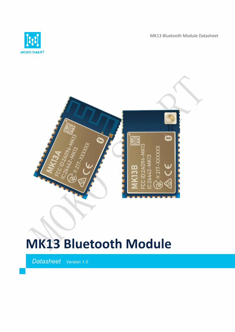
mk13 luetooth module
TRANSCRIPT
Datasheet
MK13 Bluetooth Module Datasheet
MK13 Bluetooth Module
Datasheet Version 1.0

Contents 1 Instruction 1
1.1 Features and benefits 2
1.2 Applications 2
1.3 Product options 2
1.3.1 Hardware options 2
1.3.2 Firmware options 3
1.3.3 Ordering information 3
2 Specifications 4
3 Pin assignments 6
4 Mechanical details 9
4.1 PCBA mechanical dimensions 9
4.2 PCB land pads dimensions 10
4.3 u.FL connector dimensions 10
5. Power specifications 12
5.1 Normal voltage mode 12
5.2 High voltage mode 13
6. Peripheral interfaces 14
6.1 Memory descriptions 14
6.2 Real-time counter (RTC) 14
6.3 Pulse width modulation (PWM) 15
6.4 General purpose input/output (GPIO) 16
6.5 Serial peripheral interface (SPI) 17
6.6 Universal asynchronous receiver/transmitter (UART) 18
6.7 Successive approximation analog-to-digital converter (SAADC) 19
6.8 Near field communication (NFC) 21
6.9 EasyDMA 21
7. Mounting design suggestions 23
7.1 Recommended mounting and PCB layout 23

7.2 Mechanical enclosure 24
8. Cautions 25
8.1 Reflow soldering 25
8.2 Usage condition notes 26
8.3 Storage notes 27
Revision history 28

MK13 Bluetooth Module
Datasheet
1
Copyright © 2021 MOKO TECHNOLOGY LTD.
1 Instruction
MK13 series is a powerful and highly flexible Bluetooth® 5.2 module based on Nordic® Semiconductor nRF5340 which is the world’s first wireless SoC with two Arm® Cortex®-M33 processors. The combination of two flexible processors, the advanced feature set, and an operating temperature up to 105 °C, make MK13 the ideal choice for LE Audio, professional lighting, advanced wearables, and other complex IoT applications.
The MK13 is an all-in-one Bluetooth module, including a superset of the most prominent nRF52® Series features. Features like Bluetooth® 5.2, high-speed SPI, QSPI, USB, up to 105 °C operating temperature, and more, are combined with more performance, memory and integration, while minimizing current consumption.
The MK13 module supports an extensive range of wireless protocols. It supports Bluetooth Low Energy and is capable of all angle-of-arrival (AoA) and angle-of-departure (AoD) roles in Bluetooth Direction Finding. In addition it supports LE Audio, high-throughput 2 Mbps, Advertising Extensions and Long Range. Mesh protocols like Bluetooth mesh, Thread and Zigbee can be run concurrently with Bluetooth LE, enabling smartphones to provision, commission, configure and control mesh nodes. NFC, ANT, 802.15.4 and 2.4 GHz proprietary protocols are also supported.
MK13 series modules will be programmed default MOKO MKBN series firmware and custom firmware can be programmed too.
After you choose MK13 series module, MOKOSmart will provide technical support for your development or even help you to complete all hardware and firmware design. We can power demanding applications, while simplifying designs and reducing BOM costs.
MK13 Bluetooth Module
Datasheet
2
Copyright © 2021 MOKO TECHNOLOGY LTD.
1.1 Features and benefits
• Bluetooth® 5.2
o Direction Finding
o 2Mbps
o CSA#2
o Advertising Extensions
o Long Range
• IEEE 802.15.4 radio support
o Thread
o Zigbee
• Supported data rates
o Bluetooth®: 2 Mbps, 1Mbps, 500 kbps, and 125 kbps
o IEEE 802.15.4-2006: 250kbps
o Proprietary 2.4 GHz: 2 Mbps, 1Mbps
• Wide supply voltage range: 1.7V to 5.5V
• Application core - 1MB flash and 512kB low leakage RAM
• Network core – 256kB flash and 64kB low leakage RAM
• Full set of digital interfaces including: SPI, TWI, UART, PDM, PWM, QDEC
• 12-bit, 200ksps ADC
• 128-bit AES ECB/CCM/AAR co-processor
• Individual power management for all peripherals
• On-chip DC/DC buck converter
• Dimension: 21.0 x 13.8 x 2.3mm (with shield)
1.2 Applications
• Internet of things (IOT)
o Smart home sensors and controllers
o Industrial IoT sensors and
controllers
• Advanced wearables
o Health/fitness sensor and monitor
devices
o Wireless payment enabled devices
• Wireless audio devices
o Bluetooth Low Energy Audio
o True wireless earbuds
o Headphones, microphones and
speakers
• Advanced computer peripherals and I/O
devices
o Mouse
o Keyboard
o Multi-touch trackpad
• Interactive entertainment devices
o Remote controls
o Gaming controllers
• Professional lighting
o Wireless connected luminaire
1.3 Product options
1.3.1 Hardware options
There are different module models of MK13 series Bluetooth module. All models have same dimensions and pin assignments.
MK13 Bluetooth Module
Datasheet
3
Copyright © 2021 MOKO TECHNOLOGY LTD.
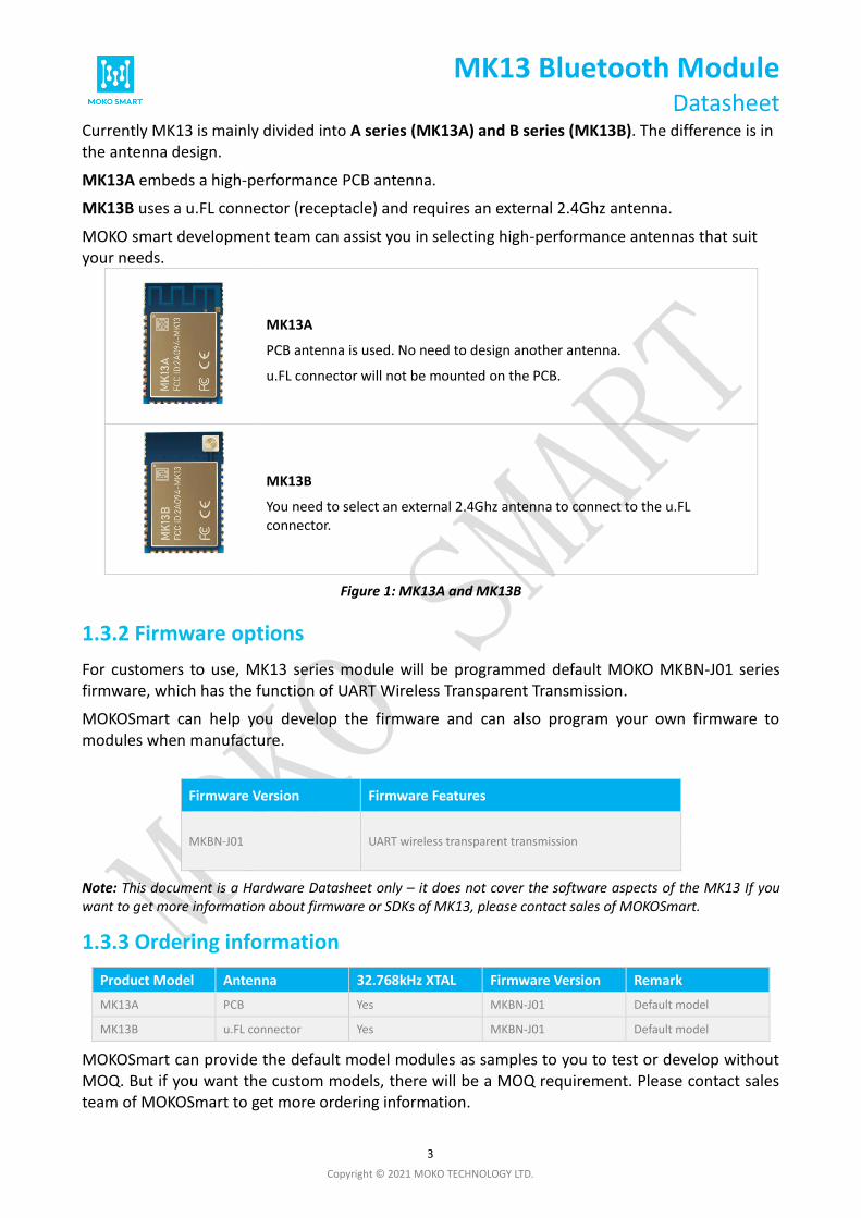
Currently MK13 is mainly divided into A series (MK13A) and B series (MK13B). The difference is in the antenna design.
MK13A embeds a high-performance PCB antenna.
MK13B uses a u.FL connector (receptacle) and requires an external 2.4Ghz antenna.
MOKO smart development team can assist you in selecting high-performance antennas that suit your needs.
MK13A
PCB antenna is used. No need to design another antenna.
u.FL connector will not be mounted on the PCB.
MK13B
You need to select an external 2.4Ghz antenna to connect to the u.FL connector.
Figure 1: MK13A and MK13B
1.3.2 Firmware options
For customers to use, MK13 series module will be programmed default MOKO MKBN-J01 series firmware, which has the function of UART Wireless Transparent Transmission.
MOKOSmart can help you develop the firmware and can also program your own firmware to modules when manufacture.
Firmware Version Firmware Features
MKBN-J01 UART wireless transparent transmission
Note: This document is a Hardware Datasheet only – it does not cover the software aspects of the MK13 If you want to get more information about firmware or SDKs of MK13, please contact sales of MOKOSmart.
1.3.3 Ordering information
Product Model Antenna 32.768kHz XTAL Firmware Version Remark
MK13A PCB Yes MKBN-J01 Default model
MK13B u.FL connector Yes MKBN-J01 Default model
MOKOSmart can provide the default model modules as samples to you to test or develop without MOQ. But if you want the custom models, there will be a MOQ requirement. Please contact sales team of MOKOSmart to get more ordering information.

MK13 Bluetooth Module
Datasheet
4
Copyright © 2021 MOKO TECHNOLOGY LTD.
2 Specifications
Detail Description
General
Application core ARM Cortex-M33 with TrustZone technology
Network core ARM Cortex-M33
Memory (Application core) 1MB flash and 512kB low leakage RAM
Memory (Network core) 256kB flash and 64kB low leakage RAM
GPIO 46 flexible General Purpose IOs
Dimensions
Length: 21mm±0.2mm
Width: 13.8mm±0.2mm
Height: 2.3mm+0.1mm/-0.15mm
Storage temperature -40 to 125°C
Operating temperature -40 to 85°C
Extended Industrial temperature -40 to +105°C can be customized
Radio
Frequency 2402MHz – 2480MHz
Wireless protocol Bluetooth Low Energy/NFC/Thread/Zigbee/802.15.4/ANT/2.4 GHz proprietary
On-air data rates
Bluetooth LE: 2 Mbps/1 Mbps/125 kbps
802.15.4: 250 kbps
Proprietary 2.4 GHz - 2 Mbps, 1 Mbps
Transmit power Programmable from +3 to -20 dBm in 1 dB steps
Receiver sensitivity
-98 dBm sensitivity in 1 Mbps Bluetooth® LE mode
-104 dBm sensitivity in 125 kbps Bluetooth® LE mode
-101 dBm sensitivity in IEEE 802.15.4
Bluetooth
Bluetooth features
Bluetooth Low Energy
Bluetooth Mesh
Bluetooth Direction Finding (AoA/AoD)
Bluetooth Low Energy Audio
1M LE PHY/ 2M LE PHY (High speed)/ LE Coded PHY (Long range)
Advertising Extensions
CSA #2 (Channel Selection Algorithm #2)
Low energy
Multiple level Low Energy state
LE L2CAP Connection Oriented Channel support
LE low duty directed advertising
LE data length extension feature
Roles Concurrent central, observer, peripheral and broadcaster
Hardware
Power supply voltage 1.7V to 5.5V
Power regulator Switching regulator for DC/DC buck setup
Output voltage 1.8 V to 3.3 V regulated supply for external components
Clock control Embedded 32MHz crystal oscillator
Embedded 32K RC oscillator and support external 32.768kHz crystal oscillator
Package 34 diameters of Half-holes + 22 LGA pads
PCB material FR-4
Impedance 50Ω

MK13 Bluetooth Module
Datasheet
5
Copyright © 2021 MOKO TECHNOLOGY LTD.
Detail Description
Antenna MK13A series – PCB trace antenna
MK13B series – u.FL connector
Interfaces
(Application core)
12 Mbps full-speed USB
2x 24-bit real-time counter (RTC)
5x SPI master/slave with EasyDMA
12-bit, 200 ksps ADC with EasyDMA - eight configurable channels with programmable gain
3x 32-bit timer with counter mode
4x I2C compatible two-wire master/slave with EasyDMA
4x pulse width modulator (PWM) units with EasyDMA
4x UART (CTS/RTS) with EasyDMA
2x Quadrature decoder (QDEC)
Near field communication (NFC-A) tag with wake-on field and touch-to-pair
Audio peripherals - I2S, digital microphone interface (PDM)
Interfaces
(Network core)
2x real-time counter (RTC)
SPI master/slave with EasyDMA
3x 32-bit timer with counter mode
I2C compatible two-wire master/slave with EasyDMA
UART (CTS/RTS) with EasyDMA
Current Consumption
System current consumption
DC/DC at 3 V
0.9 µA in System OFF
1.3 µA in System ON
1.5 µA in System ON with network core RTC running
1.7 µA in System ON with 64 KB network core RAM retained and network core RTC running
Radio current consumption
DC/DC at 3 V (TX)
5.1 mA at +3 dBm Tx power
3.4 mA at 0 dBm Tx power
Radio current consumption
DC/DC at 3 V (RX)
2.7 mA in RX at 1 Mbps
3.1 mA in RX at 2 Mbps
MK13 Bluetooth Module
Datasheet
6
Copyright © 2021 MOKO TECHNOLOGY LTD.
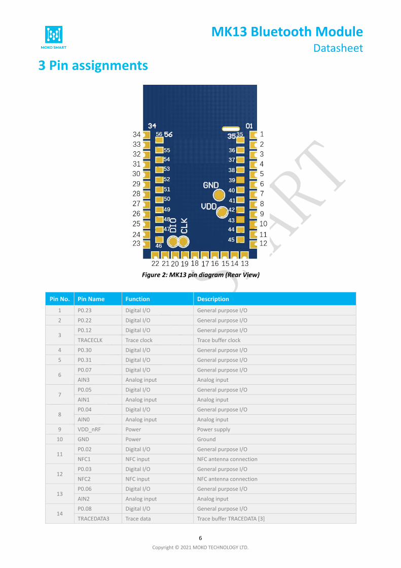
3 Pin assignments
Figure 2: MK13 pin diagram (Rear View)
Pin No. Pin Name Function Description
1 P0.23 Digital I/O General purpose I/O
2 P0.22 Digital I/O General purpose I/O
3 P0.12 Digital I/O General purpose I/O
TRACECLK Trace clock Trace buffer clock
4 P0.30 Digital I/O General purpose I/O
5 P0.31 Digital I/O General purpose I/O
6 P0.07 Digital I/O General purpose I/O
AIN3 Analog input Analog input
7 P0.05 Digital I/O General purpose I/O
AIN1 Analog input Analog input
8 P0.04 Digital I/O General purpose I/O
AIN0 Analog input Analog input
9 VDD_nRF Power Power supply
10 GND Power Ground
11 P0.02 Digital I/O General purpose I/O
NFC1 NFC input NFC antenna connection
12 P0.03 Digital I/O General purpose I/O
NFC2 NFC input NFC antenna connection
13 P0.06 Digital I/O General purpose I/O
AIN2 Analog input Analog input
14 P0.08 Digital I/O General purpose I/O
TRACEDATA3 Trace data Trace buffer TRACEDATA [3]

MK13 Bluetooth Module
Datasheet
7
Copyright © 2021 MOKO TECHNOLOGY LTD.
Pin No. Pin Name Function Description
15 P0.09 Digital I/O General purpose I/O
TRACEDATA2 Trace data Trace buffer TRACEDATA [2]
16 P0.10 Digital I/O General purpose I/O
TRACEDATA1 Trace data Trace buffer TRACEDATA [1]
17 P0.11 Digital I/O General purpose I/O
TRACEDATA0 Trace data Trace buffer TRACEDATA [0]
18 P0.13 Digital I/O General purpose I/O
IO0 IO0 for QSPI Dedicated pin for Quad SPI
19 SWDCLK Debug Serial wire debug clock input for debug and programming
20 SWDIO Debug Serial wire debug I/O for debug and programming
21 P0.14 Digital I/O General purpose I/O
IO1 IO1 for QSPI Dedicated pin for Quad SPI
22 P0.16 Digital I/O General purpose I/O
IO3 IO3 for QSPI Dedicated pin for Quad SPI
23 P0.15 Digital I/O General purpose I/O
IO2 IO2 for QSPI Dedicated pin for Quad SPI
24 P0.17 Digital I/O General purpose I/O
SCK SCK for QSPI Dedicated pin for Quad SPI
25 P0.18 Digital I/O General purpose I/O
CSN CSN for QSPI Dedicated pin for Quad SPI
26 P0.19 Digital I/O General purpose I/O
27 P0.20 Digital I/O General purpose I/O
28 P0.21 Digital I/O General purpose I/O
29 P0.24 Digital I/O General purpose I/O
30 P0.25 Digital I/O General purpose I/O
AIN4 Analog input Analog input
31 P0.26 Digital I/O General purpose I/O
AIN5 Analog input Analog input
32 P0.27 Digital I/O General purpose I/O
AIN6 Analog input Analog input
33 P0.28 Digital I/O General purpose I/O
AIN7 Analog input Analog input
34 P0.29 Digital I/O General purpose I/O
35 P1.12 Digital I/O General purpose I/O
36 P1.11 Digital I/O General purpose I/O
37 P1.15 Digital I/O General purpose I/O
38 P1.14 Digital I/O General purpose I/O
39 P1.13 Digital I/O General purpose I/O
40 P1.01 Digital I/O General purpose I/O
41 P1.00 Digital I/O General purpose I/O
42 VDDH Power Power supply
43 USB_D+ USB USB_D+
44 USB_D- USB USB_D-
45 VBUS Power 5 V input for USB 3.3 V regulator
46 P1.02 Digital I/O General purpose I/O
TWI TWI 1 Mbps High-speed pin for 1 Mbps TWI

MK13 Bluetooth Module
Datasheet
8
Copyright © 2021 MOKO TECHNOLOGY LTD.
Pin No. Pin Name Function Description
47 P1.03 Digital I/O General purpose I/O
TWI TWI 1 Mbps High-speed pin for 1 Mbps TWI
48 P1.04 Digital I/O General purpose I/O
49 P1.05 Digital I/O General purpose I/O
50 P1.06 Digital I/O General purpose I/O
51 P1.07 Digital I/O General purpose I/O
52 P1.08 Digital I/O General purpose I/O
53 P1.09 Digital I/O General purpose I/O
54 P1.10 Digital I/O General purpose I/O
55 RESET Reset Pin RESET with internal pull-up resistor
56 GND Power Ground
.

MK13 Bluetooth Module
Datasheet
9
Copyright © 2021 MOKO TECHNOLOGY LTD.
4 Mechanical details
4.1 PCBA mechanical dimensions
Figure 3: MK13 PCBA dimensions
Symbol Min. Typ. Max.
Length -0.2mm 21mm +0.2mm
Width -0.2mm 13.8mm +0.2mm
Height (PCB only) -0.08mm 0.8mm +0.08mm
Height (with shield) -0.15mm 2.3mm +0.1mm
Note: All models of MK13 series Bluetooth module have the same dimensions.

MK13 Bluetooth Module
Datasheet
10
Copyright © 2021 MOKO TECHNOLOGY LTD.
4.2 PCB land pads dimensions
Figure 4: MK13 PCB land pads dimensions (TOP View)
Symbol Typ.
Half-hole Pad (Bottom) 0.8mm x 0.8mm
LGA Square Pad 0.8mm x 0.6mm
Diameter of Half-hole 0.55mm
Diameter of Central Round pad 1mm (diameter)
4.3 u.FL connector dimensions
MK13B has mounted a micro SMT u.FL series connector (receptacle), which needs an external 2.4Ghz antenna to
connect. The model of the connector is u.FL-R-SMT-1(80).
According to the dimensions of the connector to choose an antenna with a right plug which can connect to the
receptacle appropriately.

MK13 Bluetooth Module
Datasheet
11
Copyright © 2021 MOKO TECHNOLOGY LTD.
Figure 5: u.FL-R-SMT-1(80) Dimensions
Note: More information about the u.FL connector, please refer to
https://www.hirose.com/en/product/document?clcode=&productname=&series=U.FL&documenttype=Catalog&l
ang=en&documentid=D31697_en

MK13 Bluetooth Module
Datasheet
12
Copyright © 2021 MOKO TECHNOLOGY LTD.
5. Power specifications MK13 supports two different power supply voltage ranges, each having a corresponding power supply pin. The PMU automatically activates the correct voltage regulator depending on which power supply pin is used.
5.1 Normal voltage mode
Powers the device through the VDD pin.
Figure 6: Regulator usage in normal voltage mode
The VDD and VDDH pins are connected together. The external power supply is connected to the both pins.
In this case, the VREGH regulator is automatically deactivated.
In normal voltage mode, each regulator can operate in LDO or DC/DC mode.

MK13 Bluetooth Module
Datasheet
13
Copyright © 2021 MOKO TECHNOLOGY LTD.
5.2 High voltage mode
Powers the device through the VDDH pin.
Figure 7: Regulator usage in high voltage mode
The external power supply is connected to the VDDH pin. The VREGMAIN and VREGRADIO regulators are used to power the internal circuitry from the VDD pin. The VDD pin is supplied by the VREGH regulator.
By default, the high voltage regulator is configured to also source external components from the VDD pin. To save power this feature should be disabled.
MK13 Bluetooth Module
Datasheet
14
Copyright © 2021 MOKO TECHNOLOGY LTD.
6. Peripheral interfaces
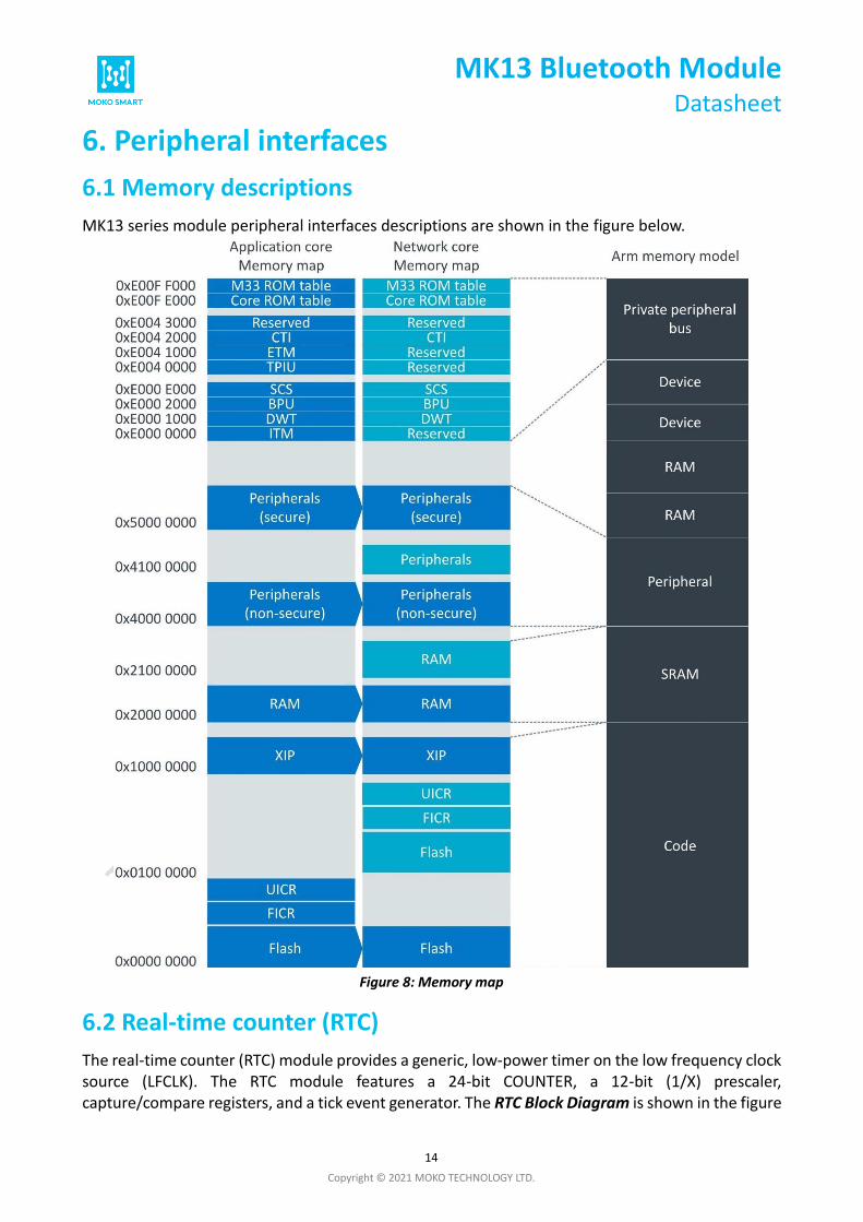
6.1 Memory descriptions
MK13 series module peripheral interfaces descriptions are shown in the figure below.
Figure 8: Memory map
6.2 Real-time counter (RTC)
The real-time counter (RTC) module provides a generic, low-power timer on the low frequency clock source (LFCLK). The RTC module features a 24-bit COUNTER, a 12-bit (1/X) prescaler, capture/compare registers, and a tick event generator. The RTC Block Diagram is shown in the figure

MK13 Bluetooth Module
Datasheet
15
Copyright © 2021 MOKO TECHNOLOGY LTD.
below.
The RTC Features:
• 12-bits pre-scale counter
• 24-bits read only RTC counter
• 32.768kHz XTAL or RC oscillator clock resource
• Independent comparators (with interrupt)
• 1 tick interrupt
• RTC counter overflow interrupt
Figure 9: RTC Block Diagram
6.3 Pulse width modulation (PWM)
MK13 supports 4 PWM modules. The pulse width modulation (PWM) module enables the generation of pulse width modulated signals on GPIO. The module implements an up or up-and-down counter with four PWM channels that drive assigned GPIOs.
The following are the main features of a PWM module:
• Programmable PWM frequency
• Up to four PWM channels with individual polarity and duty cycle values
• Edge or center-aligned pulses across PWM channels
• Multiple duty cycle arrays (sequences) defined in RAM
• Autonomous and glitch-free update of duty cycle values directly from memory through EasyDMA (no CPU involvement)
• Change of polarity, duty cycle, and base frequency possibly on every PWM period
• RAM sequences can be repeated or connected into loops

MK13 Bluetooth Module
Datasheet
16
Copyright © 2021 MOKO TECHNOLOGY LTD.
Figure 10: PWM module
6.4 General purpose input/output (GPIO)
MK13 series module provides highly flexible GPIOs for development. The general purpose input/output pins (GPIOs) are grouped as one or more ports with each port having up to 32 GPIOs. The GPIO port and the GPIO pin details is shown in the figure below.
The GPIO Features:
• Up to 32 GPIO pins per GPIO port
• Configurable output drive strength
• Internal pull-up and pull-down resistors
• Wake-up from high or low level triggers on all pins
• Trigger interrupt on state changes on any pin
• All pins can be used by the PPI task/event system
• One or more GPIO outputs can be controlled through PPI and GPIOTE channels
• All pins can be individually mapped to interface blocks for layout flexibility
• GPIO state changes captured on SENSE signal can be stored by LATCH register
• Pin sharing in multi-MCU system
• Support for secure and non-secure attributes for pins in conjunction with the system protection unit
MK13 Bluetooth Module
Datasheet
17
Copyright © 2021 MOKO TECHNOLOGY LTD.
Figure 11: GPIO port and the GPIO pin details
Note: The MK13 module has a built-in 32.768kHz oscillator which occupies P0.00 and P0.01.
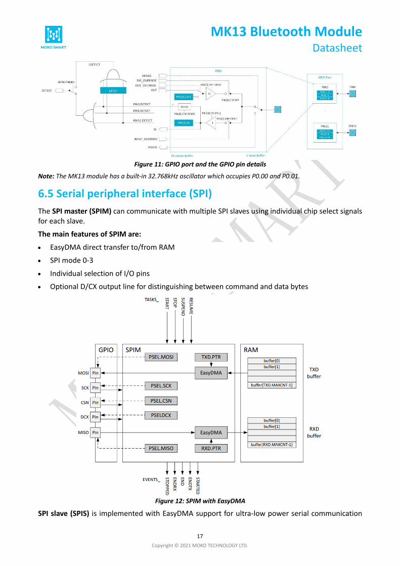
6.5 Serial peripheral interface (SPI)
The SPI master (SPIM) can communicate with multiple SPI slaves using individual chip select signals for each slave.
The main features of SPIM are:
• EasyDMA direct transfer to/from RAM
• SPI mode 0-3
• Individual selection of I/O pins
• Optional D/CX output line for distinguishing between command and data bytes
Figure 12: SPIM with EasyDMA
SPI slave (SPIS) is implemented with EasyDMA support for ultra-low power serial communication

MK13 Bluetooth Module
Datasheet
18
Copyright © 2021 MOKO TECHNOLOGY LTD.
from an external SPI master. EasyDMA in conjunction with hardware-based semaphore mechanisms removes all real-time requirements associated with controlling the SPI slave from a low priority CPU execution context.
Figure 13: SPI slave
6.6 Universal asynchronous receiver/transmitter (UART)
The GPIOs used for each UART interface can be chosen from any GPIO on the device and are independently configurable. This enables device pinout flexibility and efficient use of board space and signal routing.
The main features of UARTE are the following:
• Full-duplex operation
• Automatic hardware flow control
• Optional even parity bit checking and generation
• EasyDMA
• Up to 1 Mbps baudrate

MK13 Bluetooth Module
Datasheet
19
Copyright © 2021 MOKO TECHNOLOGY LTD.
• Return to IDLE between transactions supported (when using HW flow control)
• One or two stop bit
• Least significant bit (LSB) first
Figure 14: UART configuration
Note: The external crystal oscillator must be enabled to obtain sufficient clock accuracy for stable
communication.
6.7 Successive approximation analog-to-digital converter (SAADC)
SAADC is a differential successive approximation register (SAR) analog-to-digital converter (ADC).
The main features of SAADC are the following:
• 8/10/12-bit resolution, 14-bit resolution with oversampling
• Multiple analog inputs:
AIN0 to AIN7 pins
VDD pin
VDDHDIV5 (through VDDH pin)
• Up to eight input channels:
One channel per single-ended input and two channels per differential input
Scan mode can be configured with both single-ended channels and differential channels
Each channel can be configured to select any of the above analog inputs
• Full scale input range (0 to VDD)
• Sampling triggered via a task from software or a PPI channel for full flexibility on sample frequency source from a low-power 32.768 kHz RTC or more accurate 1/16 MHz timers
• One-shot conversion mode to sample a single channel
• Scan mode to sample a series of channels in sequence with configurable sample delay

MK13 Bluetooth Module
Datasheet
20
Copyright © 2021 MOKO TECHNOLOGY LTD.
• Support for direct sample transfer to RAM using EasyDMA
• Interrupts on single sample and full buffer events
• Samples stored as 16-bit two’s complement values for differential and single-ended sampling
• Continuous sampling without the need of an external timer
• Internal resistor string
• On-the-fly limit checking
Figure 15: Simplified ADC block diagram
ADC Pin:
Pin No. Pin Name ADC channel
45 P0.04 Analog input 0
44 P0.05 Analog input 1
14 P0.06 Analog input 2
4 P0.07 Analog input 3
53 P0.25 Analog input 4
31 P0.26 Analog input 5
54 P0.27 Analog input 6
32 P0.28 Analog input 7

MK13 Bluetooth Module
Datasheet
21
Copyright © 2021 MOKO TECHNOLOGY LTD.
6.8 Near field communication (NFC)
MK13 supply near field communication (NFC-A) tag with wake-on field and touch-to-pair.
The NFCT peripheral is an implementation of an NFC Forum compliant listening device NFC-A.
With appropriate software, the NFC peripheral can be used as the listening device NFC-A as specified by the NFC Forum.
Listed here are the main features for the NFC peripheral:
• NFC-A listen mode operation
• 13.56 MHz input frequency
• Bit rate 106 kbps
• Wake-on-field low power field detection (SENSE) mode
• Frame assemble and disassemble for the NFC-A frames specified by the NFC Forum
• Programmable frame timing controller
• Integrated automatic collision resolution, cyclic redundancy check (CRC), and parity functions.
Figure 16: NFC block diagram
6.9 EasyDMA
EasyDMA is a module implemented by some peripherals to gain direct access to Data RAM.

MK13 Bluetooth Module
Datasheet
22
Copyright © 2021 MOKO TECHNOLOGY LTD.
EasyDMA is an AHB bus master similar to CPU and is connected to the AHB multilayer interconnect
for direct access to Data RAM. EasyDMA cannot access flash memory.
A peripheral can implement multiple EasyDMA instances to provide dedicated channels. For
example, for reading and writing of data between the peripheral and RAM. This concept is
illustrated in the following figure
Figure 17: EasyDMA example

MK13 Bluetooth Module
Datasheet
23
Copyright © 2021 MOKO TECHNOLOGY LTD.
7. Mounting design suggestions
7.1 Recommended mounting and PCB layout
You can refer to the following references for the mounting design and PCB layout of the MK13 module, especially for the MK13A model which has PCB on-board antenna.
For external antenna modules (MK13B needs to connect an external antenna to the u.FL connector), you also need to refer to the external antenna design requirements.
The recommended mounting and PCB layout suggestion:
• Locate MK13 series module close to the edge of the host PCB (mandatory for MK13A for on-board PCB trace antenna to radiate properly).
• Ensure there is no copper in the antenna keep-out area on any layers of the host PCB. Keep all mounting hardware and metal clear of the area to allow proper antenna radiation.
• Keep the antenna area as far away as possible from the power supply and metal components.
• Ensure no exposed copper is on the underside of the module.
• A different host PCB thickness dielectric will have small effect on antenna.
• Use solid GND plane on inner layer (for best EMC and RF performance).
• All module GND pins must be connected to the host PCB GND.
• Place GND vias close to module GND pads as possible.
• Unused PCB area on surface layer can flooded with copper but place GND vias regularly to connect the copper flood to the inner GND plane. If GND flood copper is on the bottom of the module, then connect it with GND vias to the inner GND plane.
• Use a good layout method to avoid excessive noise coupling with signal lines or supply voltage lines.
Figure 18: Recommended Module Mounting Examples

MK13 Bluetooth Module
Datasheet
24
Copyright © 2021 MOKO TECHNOLOGY LTD.
7.2 Mechanical enclosure
Care should be taken when designing and placing the MK13 series module into an enclosure. Metal should be kept clear from the antenna area, both above and below. Any metal around the module can negatively impact RF performance.
The module is designed and tuned for the antenna and RF components to be in free air. Any potting, epoxy fill, plastic over-molding, or conformal coating can negatively impact RF performance and must be evaluated by the customer.
Placement of metal/plastic enclosure:
• Minimum safe distance for metal parts without seriously compromising the antenna (tuning) is 40 mm top/bottom and 30 mm left or right.
• Metal close to the MK13 series module antenna (bottom, top, left, right, any direction) will have degradation on the antenna performance. The amount of that degradation is entirely system dependent, meaning you will need to perform some testing with your host application.
• Any metal closer than 20 mm will begin to significantly degrade performance (S11, gain, radiation efficiency).
• It is best that you test the range with a mock-up (or actual prototype) of the product to assess effects of enclosure height (and materials, whether metal or plastic).
MK13 Bluetooth Module
Datasheet
25
Copyright © 2021 MOKO TECHNOLOGY LTD.
8. Cautions
8.1 Reflow soldering
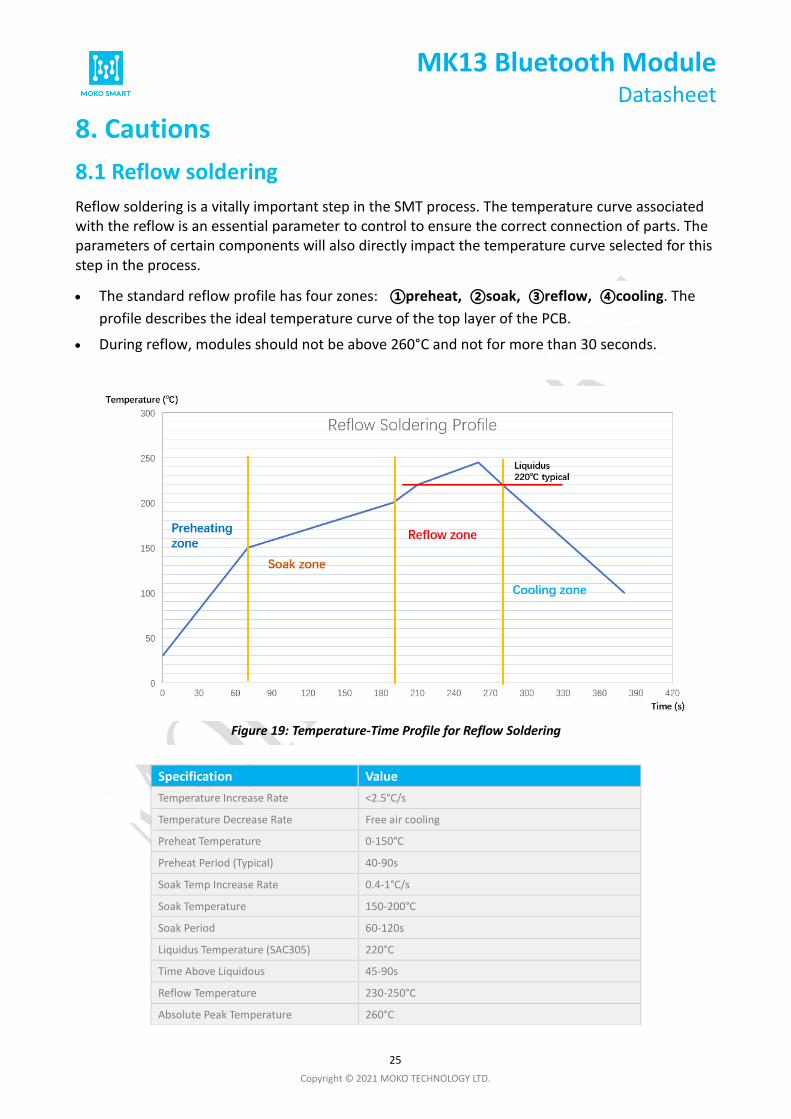
Reflow soldering is a vitally important step in the SMT process. The temperature curve associated with the reflow is an essential parameter to control to ensure the correct connection of parts. The parameters of certain components will also directly impact the temperature curve selected for this step in the process.
• The standard reflow profile has four zones: ①preheat, ②soak, ③reflow, ④cooling. The
profile describes the ideal temperature curve of the top layer of the PCB.
• During reflow, modules should not be above 260°C and not for more than 30 seconds.
Figure 19: Temperature-Time Profile for Reflow Soldering
Specification Value
Temperature Increase Rate <2.5°C/s
Temperature Decrease Rate Free air cooling
Preheat Temperature 0-150°C
Preheat Period (Typical) 40-90s
Soak Temp Increase Rate 0.4-1°C/s
Soak Temperature 150-200°C
Soak Period 60-120s
Liquidus Temperature (SAC305) 220°C
Time Above Liquidous 45-90s
Reflow Temperature 230-250°C
Absolute Peak Temperature 260°C

MK13 Bluetooth Module
Datasheet
26
Copyright © 2021 MOKO TECHNOLOGY LTD.
Figure 20: Example of MOKO Smart SMT reflow soldering
8.2 Usage condition notes
• Follow the conditions written in this specification, especially the recommended condition ratings about the power supply applied to this product.
• The supply voltage has to be free of AC ripple voltage (for example from a battery or a low noise regulator output). For noisy supply voltages, provide a decoupling circuit (for example a ferrite in series connection and a bypass capacitor to ground of at least 47Uf directly at the module).
• Take measures to protect the unit against static electricity. If pulses or other transient loads (a large load applied in a short time) are applied to the products, check and evaluate their operation before assembly on the final products.
• The supply voltage should not be exceedingly high or reversed. It should not carry noise and/or spikes.
• This product away from other high frequency circuits.
• Keep this product away from heat. Heat is the major cause of decreasing the life of these products.
• Avoid assembly and use of the target equipment in conditions where the products’ temperature may exceed the maximum tolerance.
• This product should not be mechanically stressed when installed.
MK13 Bluetooth Module
Datasheet
27
Copyright © 2021 MOKO TECHNOLOGY LTD.
• Do not use dropped products.
• Do not touch, damage or soil the pins.
• Pressing on parts of the metal shield or fastening objects to the metal shield will cause damage.
8.3 Storage notes
• The module should not be stressed mechanically during storage.
• Do not store these products in the following conditions or the performance characteristics of the product, such as RF performance will be adversely affected:
o Storage in salty air or in an environment with a high concentration of corrosive gas.
o Storage in direct sunlight
o Storage in an environment where the temperature may be outside the range specified.
o Storage of the products for more than one year after the date of delivery storage period.
• Keep this product away from water, poisonous gas and corrosive gas.
• This product should not be stressed or shocked when transported.

MK13 Bluetooth Module
Datasheet
28
Copyright © 2021 MOKO TECHNOLOGY LTD.
Revision history
Version Comments Contributor(s) Revision Date
V0.1 Draft release Victor Chow 2021/08/02
V1.0 Proofreading draft and modify some errors Kevin Huang 2021/08/18
The contents of this datasheet are subject to change without prior notice for further improvement. MOKO team reserves all the rights for the final explanation.
Please contact MOKO sales team or visit https://www.mokoblue.com to get more related information if needed.
MOKO TECHNOLOGY LTD.
4F,Buidling2, Guanghui Technology Park,
MinQing Rd, Longhua, Shenzhen, Guangdong, China
Tel:86-755-23573370-829
https://www.mokoblue.com
https://www.mokosmart.com