mips isa and single cycle datapath - duke database...
TRANSCRIPT

cps 104 1
MIPS ISA and Single Cycle Datapath
Computer Science 104
cps 104 2
Outline of Today’s Lecture
Homework #5
The MIPS Instruction Set
Datapath and timing for Reg-Reg Operations
Datapath for Logical Operations with Immediate
Datapath for Load and Store Operations
Datapath for Branch and Jump Operations

cps 104 3
The MIPS Instruction Formats
° All MIPS instructions are 32 bits long. The three instruction formats: • R-type • I-type • J-type
° The different fields are: • op: operation of the instruction • rs, rt, rd: the source and destination register specifiers • shamt: shift amount • funct: selects the variant of the operation in the “op” field • address / immediate: address offset or immediate value • target address: target address of the jump instruction
op target address 0 26 31
6 bits 26 bits
op rs rt rd shamt funct 0 6 11 16 21 26 31
6 bits 6 bits 5 bits 5 bits 5 bits 5 bits
op rs rt immediate 0 16 21 26 31
6 bits 16 bits 5 bits 5 bits
cps 104 4
The MIPS Subset (We can’t implement them all!)
° ADD and subtract • add rd, rs, rt • sub rd, rs, rt
° OR Immediate: • ori rt, rs, imm16
° LOAD and STORE • lw rt, rs, imm16 • sw rt, rs, imm16
° BRANCH: • beq rs, rt, imm16
° JUMP: • j target op target address
0 26 31
6 bits 26 bits
op rs rt rd shamt funct 0 6 11 16 21 26 31
6 bits 6 bits 5 bits 5 bits 5 bits 5 bits
op rs rt immediate 0 16 21 26 31
6 bits 16 bits 5 bits 5 bits
cps 104 5
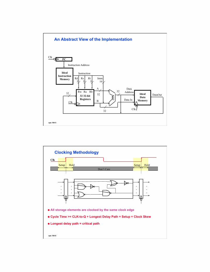
An Abstract View of the Implementation
Clk
5
Rw Ra Rb 32 32-bit Registers
Rd
AL
U
Clk
Data In
DataOut
Data Address
Ideal Data
Memory
Instruction
Instruction Address
Ideal Instruction
Memory
Clk PC
5 Rs
5 Rt
16 Imm
32
32 32 32
A
B
cps 104 6
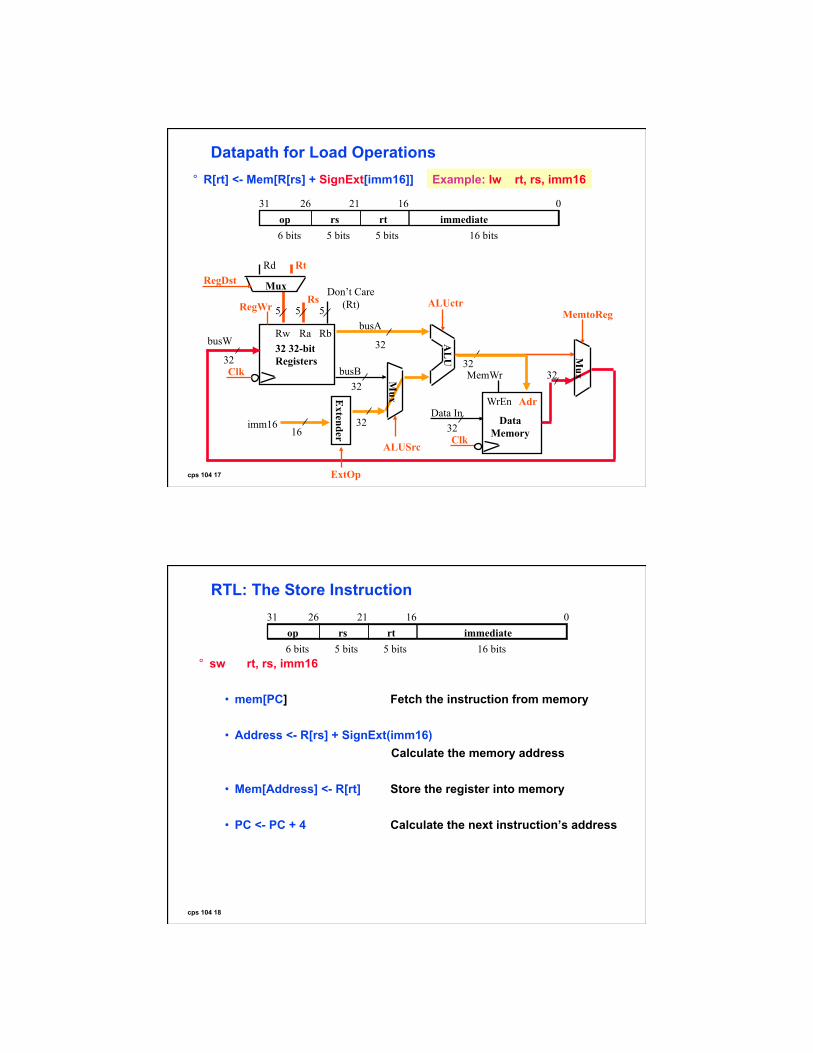
Clocking Methodology
All storage elements are clocked by the same clock edge
Cycle Time >= CLK-to-Q + Longest Delay Path + Setup + Clock Skew
Longest delay path = critical path
Clk
Don’t Care Setup Hold
.
.
.
.
.
.
.
.
.
.
.
.
Setup Hold

cps 104 7
An Abstract View of the Critical Path ° Register file and ideal memory:
• The CLK input is a factor ONLY during write operation • During read operation, behave as combinational logic:
- Address valid => Output valid after “access time.”
Clk
5
Rw Ra Rb 32 32-bit Registers
Rd
AL
U
Clk
Data In
DataOut
Data Address
Ideal Data
Memory
Instruction
Instruction Address
Ideal Instruction
Memory
Clk PC
5 Rs
5 Rt
16 Imm
32
32 32 32
cps 104 8
Overview of the Instruction Fetch Unit
° The common RTL operations • Fetch the Instruction: mem[PC] • Update the program counter:
- Sequential Code: PC <- PC + 4 - Branch and Jump: PC <- “something else”
32
Instruction Word Address
Instruction Memory
PC Clk
Next Address Logic

cps 104 9
RTL: The ADD Instruction
° add rd, rs, rt • mem[PC] Fetch the instruction from memory • R[rd] <- R[rs] + R[rt] The ADD operation • PC <- PC + 4 Calculate the next instruction’s address
cps 104 10
RTL: The Load Instruction
° lw rt, rs, imm16 • mem[PC] Fetch the instruction from memory • Address <- R[rs] + SignExt(imm16) Calculate the memory address • R[rt] <- Mem[Address] Load the data into the register • PC <- PC + 4 Calculate the next instruction’s address

cps 104 11
RTL: The ADD Instruction
° add rd, rs, rt • mem[PC] Fetch the instruction from memory • R[rd] <- R[rs] + R[rt] The actual operation • PC <- PC + 4 Calculate the next instruction’s address
op rs rt rd shamt funct 0 6 11 16 21 26 31
6 bits 6 bits 5 bits 5 bits 5 bits 5 bits
cps 104 12
RTL: The Subtract Instruction
° sub rd, rs, rt • mem[PC] Fetch the instruction from memory • R[rd] <- R[rs] - R[rt] The actual operation • PC <- PC + 4 Calculate the next instruction’s address
op rs rt rd shamt funct 0 6 11 16 21 26 31
6 bits 6 bits 5 bits 5 bits 5 bits 5 bits

cps 104 13
Datapath for Register-Register Operations ° R[rd] <- R[rs] op R[rt] Example: add rd, rs, rt
• Ra, Rb, and Rw comes from instruction’s rs, rt, and rd fields • ALUctr and RegWr: control logic after decoding the instruction
fields: op and func
32
Result
ALUctr
Clk
busW
RegWr
32 32
busA
32 busB
5 5 5
Rw Ra Rb 32 32-bit Registers
Rs Rt Rd A
LU
op rs rt rd shamt funct 0 6 11 16 21 26 31
6 bits 6 bits 5 bits 5 bits 5 bits 5 bits
cps 104 14
RTL: The OR Immediate Instruction
° ori rt, rs, imm16 • mem[PC] Fetch the instruction from memory • R[rt] <- R[rs] or ZeroExt(imm16) The OR operation • PC <- PC + 4 Calculate the next instruction’s address
immediate 0 16 15 31
16 bits 16 bits 0 0 0 0 0 0 0 0 0 0 0 0 0 0 0 0
op rs rt immediate 0 16 21 26 31
6 bits 16 bits 5 bits 5 bits

cps 104 15
Datapath for Logical Operations with Immediate ° R[rt] <- R[rs] op ZeroExt[imm16]] Example: ori rt, rs, imm16
32
Result
ALUctr
Clk
busW
RegWr
32 32
busA
32 busB
5 5 5
Rw Ra Rb 32 32-bit Registers
Rs
Rt
Don’t Care (Rt)
Rd RegDst
ZeroE
xt
Mux
Mux
32 16 imm16
ALUSrc
AL
U
op rs rt immediate 0 16 21 26 31
6 bits 16 bits 5 bits 5 bits
cps 104 16
RTL: The Load Instruction
° lw rt, rs, imm16 • mem[PC] Fetch the instruction from memory • Address <- R[rs] + SignExt(imm16) Calculate the memory address R[rt] <- Mem[Address] Load the data into the register
• PC <- PC + 4 Calculate the next instruction’s address
immediate 0 16 15 31
16 bits 16 bits 0 0 0 0 0 0 0 0 0 0 0 0 0 0 0 0 0
0 16 15 31 immediate
16 bits 16 bits 1 1 1 1 1 1 1 1 1 1 1 1 1 1 1 1 1
op rs rt immediate 0 16 21 26 31
6 bits 16 bits 5 bits 5 bits
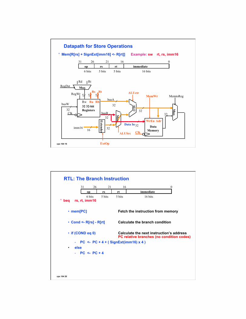
cps 104 17
Datapath for Load Operations ° R[rt] <- Mem[R[rs] + SignExt[imm16]] Example: lw rt, rs, imm16
op rs rt immediate 0 16 21 26 31
6 bits 16 bits 5 bits 5 bits
32
ALUctr
Clk
busW
RegWr
32 32
busA
32 busB
5 5 5
Rw Ra Rb 32 32-bit Registers
Rs
Rt
Don’t Care (Rt)
Rd RegDst
Extender
Mux
Mux
32 16
imm16
ALUSrc
ExtOp
Mux
MemtoReg
Clk
Data In WrEn
32
Adr
Data Memory
32 A
LU
MemWr
cps 104 18
RTL: The Store Instruction
° sw rt, rs, imm16 • mem[PC] Fetch the instruction from memory • Address <- R[rs] + SignExt(imm16) Calculate the memory address • Mem[Address] <- R[rt] Store the register into memory • PC <- PC + 4 Calculate the next instruction’s address
op rs rt immediate 0 16 21 26 31
6 bits 16 bits 5 bits 5 bits
cps 104 19
Datapath for Store Operations ° Mem[R[rs] + SignExt[imm16] <- R[rt]] Example: sw rt, rs, imm16
32
ALUctr
Clk
busW
RegWr
32 32
busA
32 busB
5 5 5
Rw Ra Rb 32 32-bit Registers
Rs
Rt
Rt
Rd RegDst
Extender
Mux
Mux
32 16 imm16
ALUSrc
ExtOp
Mux
MemtoReg
Clk
Data In WrEn
32 Adr
Data Memory
32
MemWr
AL
U
op rs rt immediate 0 16 21 26 31
6 bits 16 bits 5 bits 5 bits
cps 104 20
RTL: The Branch Instruction
° beq rs, rt, imm16 • mem[PC] Fetch the instruction from memory • Cond <- R[rs] - R[rt] Calculate the branch condition • if (COND eq 0) Calculate the next instruction’s address
PC relative branches (no condition codes) - PC <- PC + 4 + ( SignExt(imm16) x 4 )
• else - PC <- PC + 4
op rs rt immediate 0 16 21 26 31
6 bits 16 bits 5 bits 5 bits

cps 104 21
Datapath for Branch Operations ° beq rs, rt, imm16 We need to compare Rs and Rt!
op rs rt immediate 0 16 21 26 31
6 bits 16 bits 5 bits 5 bits
ALUctr
Clk
busW
RegWr
32 32
busA
32 busB
5 5 5
Rw Ra Rb 32 32-bit Registers
Rs
Rt
Rt
Rd RegDst
Extender
Mux
Mux
32 16
imm16
ALUSrc
ExtOp
AL
U
PC Clk
Next Address Logic 16
imm16
Branch
To Instruction Memory
Zero
cps 104 22
Binary Arithmetic for the Next Address
° In theory, the PC is a 32-bit byte address into the instruction memory: • Sequential operation: PC<31:0> = PC<31:0> + 4 • Branch operation: PC<31:0> = PC<31:0> + 4 + SignExt[Imm16] * 4
° The magic number “4” always comes up because: • The 32-bit PC is a byte address • And all our instructions are 4 bytes (32 bits) long
° In other words: • The 2 LSBs of the 32-bit PC are always zeros • There is no reason to have hardware to keep the 2 LSBs
° In practice, we can simplify the hardware by using a 30-bit PC<31:2>: • Sequential operation: PC<31:2> = PC<31:2> + 1 • Branch operation: PC<31:2> = PC<31:2> + 1 + SignExt[Imm16] • In either case: Instruction-Memory-Address = PC<31:2> concat “00”

cps 104 23
Next Address Logic: Expensive and Fast Solution
° Using a 30-bit PC: • Sequential operation: PC<31:2> = PC<31:2> + 1 • Branch operation: PC<31:2> = PC<31:2> + 1 + SignExt[Imm16] • In either case: Instruction-Memory-Address = PC<31:2> concat “00”
30 30
SignExt
30
16 imm16
Mux
0
1
Adder
“1”
PC
Clk
Adder 30
30
Branch Zero
Addr<31:2>
Instruction Memory
Addr<1:0> “00”
32
Instruction<31:0> Instruction<15:0>
30
cps 104 24
Next Address Logic
30
30 SignExt
30 16 imm16
Mux
0
1
Adder
“0”
PC
Clk
30
Branch Zero
Addr<31:2>
Instruction Memory
Addr<1:0> “00”
32
Instruction<31:0>
30
“1”
Carry In
Instruction<15:0>
cps 104 25
RTL: The Jump Instruction
° j target • mem[PC] Fetch the instruction from memory • PC <- PC+4<31:28> concat target<25:0> concat <00> Calculate the next instruction’s address
op target address 0 26 31
6 bits 26 bits
cps 104 26
Instruction Fetch Unit
30 30
SignExt
30
16 imm16
Mux
0
1
Adder “1”
PC
Clk
Adder
30
30
Branch Zero
“00”
Addr<31:2>
Instruction Memory
Addr<1:0>
32
Mux
1
0
26
4 PC+4<31:28>
Target 30
° j target • PC<31:2> <- PC+4<31:28> concat target<25:0>
Jump
Instruction<15:0>
Instruction<31:0>
30
Instruction<25:0>

cps 104 27
Putting it All Together: A Single Cycle Datapath
32
ALUctr
Clk
busW
RegWr
32 32
busA
32 busB
5 5 5
Rw Ra Rb 32 32-bit Registers
Rs
Rt
Rt
Rd RegDst
Extender
Mux
Mux
32 16 imm16
ALUSrc
ExtOp
Mux
MemtoReg
Clk
Data In WrEn
32 Adr
Data Memory
32
MemWr
AL
U
Instruction Fetch Unit
Clk
Zero
Instruction<31:0>
Jump
Branch
° We have everything except control signals.
0
1
0
1
0 1
<21:25>
<16:20>
<11:15>
<0:15>
Imm16 Rd Rs Rt
cps 104 28
Recap: The MIPS Instruction Formats
° All MIPS instructions are 32 bits long. The three instruction formats: • R-type • I-type • J-type
° The different fields are: • op: operation of the instruction • rs, rt, rd: the source and destination registers specifier • shamt: shift amount • funct: selects the variant of the operation in the “op” field • address / immediate: address offset or immediate value • target address: target address of the jump instruction
op target address 0 26 31
6 bits 26 bits
op rs rt rd shamt funct 0 6 11 16 21 26 31
6 bits 6 bits 5 bits 5 bits 5 bits 5 bits
op rs rt immediate 0 16 21 26 31
6 bits 16 bits 5 bits 5 bits

cps 104 29
Recap: The MIPS Subset
° ADD and subtract • add rd, rs, rt • sub rd, rs, rt
° OR Imm: • ori rt, rs, imm16
° LOAD and STORE • lw rt, rs, imm16 • sw rt, rs, imm16
° BRANCH: • beq rs, rt, imm16
° JUMP: • j target op target address
0 26 31
6 bits 26 bits
op rs rt rd shamt funct 0 6 11 16 21 26 31
6 bits 6 bits 5 bits 5 bits 5 bits 5 bits
op rs rt immediate 0 16 21 26 31
6 bits 16 bits 5 bits 5 bits
cps 104 30
RTL: The ADD Instruction
° add rd, rs, rt • mem[PC] Fetch the instruction from memory • R[rd] <- R[rs] + R[rt] The actual operation • PC <- PC + 4 Calculate the next instruction’s address
op rs rt rd shamt funct 0 6 11 16 21 26 31
6 bits 6 bits 5 bits 5 bits 5 bits 5 bits

cps 104 31
Instruction Fetch Unit at the Beginning of Add / Subtract
30 30
SignExt
30
16 imm16
Mux
0
1
Adder “1”
PC
Clk
Adder
30
30
Branch = previous Zero = previous
“00”
Addr<31:2>
Instruction Memory
Addr<1:0>
32 M
ux
1
0
26
4 PC<31:28>
Target 30
° Fetch the instruction from Instruction memory: Instruction <- mem[PC] • This is the same for all instructions
Jump = previous
Instruction<15:0>
Instruction<31:0>
30
Instruction<25:0>
cps 104 32
The Single Cycle Datapath during Add and Subtract
32
ALUctr = Add or Subtract
Clk
busW
RegWr = 1
32 32
busA
32 busB
5 5 5
Rw Ra Rb 32 32-bit Registers
Rs
Rt
Rt
Rd RegDst = 1
Extender
Mux
Mux
32 16 imm16
ALUSrc = 0
ExtOp = x
Mux
MemtoReg = 0
Clk
Data In WrEn
32 Adr
Data Memory
32
MemWr = 0
AL
U
Instruction Fetch Unit
Clk
Zero
Instruction<31:0>
Jump = 0
Branch = 0
° R[rd] <- R[rs] + / - R[rt]
0
1
0
1
0 1
<21:25>
<16:20>
<11:15>
<0:15>
Imm16 Rd Rs Rt
op rs rt rd shamt funct 0 6 11 16 21 26 31

cps 104 33
Instruction Fetch Unit at the End of Add and Subtract
30 30
SignExt
30
16 imm16
Mux
0
1
Adder “1”
PC
Clk
Adder
30
30
Branch = 0 Zero = x
“00”
Addr<31:2>
Instruction Memory
Addr<1:0>
32 M
ux
1
0
26
4 PC<31:28>
Target 30
° PC <- PC + 4 • This is the same for all instructions except: Branch and Jump
Jump = 0
Instruction<15:0>
Instruction<31:0>
30
Instruction<25:0>
cps 104 34
The Single Cycle Datapath during Or Immediate
32
ALUctr = Or
Clk
busW
RegWr = 1
32 32
busA
32 busB
5 5 5
Rw Ra Rb 32 32-bit Registers
Rs
Rt
Rt
Rd RegDst = 0
Extender
Mux
Mux
32 16 imm16
ALUSrc = 1
ExtOp = 0
Mux
MemtoReg = 0
Clk
Data In WrEn
32 Adr
Data Memory
32
MemWr = 0
AL
U
Instruction Fetch Unit
Clk
Zero
Instruction<31:0>
Jump = 0
Branch = 0
° R[rt] <- R[rs] or ZeroExt[Imm16]
0
1
0
1
0 1
<21:25>
<16:20>
<11:15>
<0:15>
Imm16 Rd Rs Rt
op rs rt immediate 0 16 21 26 31

cps 104 35
The Single Cycle Datapath during Load
32
ALUctr = Add
Clk
busW
RegWr = 1
32 32
busA
32 busB
5 5 5
Rw Ra Rb 32 32-bit Registers
Rs
Rt
Rt
Rd RegDst = 0
Extender
Mux
Mux
32 16 imm16
ALUSrc = 1
ExtOp = 1
Mux
MemtoReg = 1
Clk
Data In WrEn
32 Adr
Data Memory
32
MemWr = 0
AL
U
Instruction Fetch Unit
Clk
Zero
Instruction<31:0>
Jump = 0
Branch = 0
0
1
0
1
0 1
<21:25>
<16:20>
<11:15>
<0:15>
Imm16 Rd Rs Rt
° R[rt] <- Data Memory {R[rs] + SignExt[imm16]}
op rs rt immediate 0 16 21 26 31
cps 104 36
The Single Cycle Datapath during Store (fill it in)
32
ALUctr
Clk
busW
RegWr =
32 32
busA
32 busB
5 5 5
Rw Ra Rb 32 32-bit Registers
Rs
Rt
Rt
Rd RegDst =
Extender
Mux
Mux
32 16 imm16
ALUSrc =
ExtOp =
Mux
MemtoReg =
Clk
Data In WrEn
32 Adr
Data Memory
32
MemWr =
AL
U
Instruction Fetch Unit
Clk
Zero
Instruction<31:0>
Jump =
Branch =
0
1
0
1
0 1
<21:25>
<16:20>
<11:15>
<0:15>
Imm16 Rd Rs Rt
° Data Memory {R[rs] + SignExt[imm16]} <- R[rt]
op rs rt immediate 0 16 21 26 31

cps 104 37
The Single Cycle Datapath during Branch
32
ALUctr = Subtract
Clk
busW
RegWr = 0
32 32
busA
32 busB
5 5 5
Rw Ra Rb 32 32-bit Registers
Rs
Rt
Rt
Rd RegDst = x
Extender
Mux
Mux
32 16 imm16
ALUSrc = 0
ExtOp = x
Mux
MemtoReg = x
Clk
Data In WrEn
32 Adr
Data Memory
32
MemWr = 0
AL
U
Instruction Fetch Unit
Clk
Zero
Instruction<31:0>
Jump = 0
Branch = 1
0
1
0
1
0 1
<21:25>
<16:20>
<11:15>
<0:15>
Imm16 Rd Rs Rt
° if (R[rs] - R[rt] == 0) then Zero <- 1 ; else Zero <- 0
op rs rt immediate 0 16 21 26 31
cps 104 38
Instruction Fetch Unit at the End of Branch
30 30
SignExt
30
16 imm16
Mux
0
1
Adder “1”
PC
Clk
Adder
30
30
Branch = 1 Zero = 1
“00”
Addr<31:2>
Instruction Memory
Addr<1:0>
32
Mux
1
0 26
4 PC<31:28>
Target 30
Jump = 0
Instruction<15:0>
Instruction<31:0>
30
Instruction<25:0>
° if (Zero == 1) then PC = PC + 4 + SignExt[imm16]*4 ; else PC = PC + 4
op rs rt immediate 0 16 21 26 31
Assume Zero = 1 to see the interesting case.

cps 104 39
The Single Cycle Datapath during Jump
32
ALUctr = x
Clk
busW
RegWr = 0
32 32
busA
32 busB
5 5 5
Rw Ra Rb 32 32-bit Registers
Rs
Rt
Rt
Rd RegDst = x
Extender
Mux
Mux
32 16 imm16
ALUSrc = x
ExtOp = x
Mux
MemtoReg = x
Clk
Data In WrEn
32 Adr
Data Memory
32
MemWr = 0
AL
U
Instruction Fetch Unit
Clk
Zero
Instruction<31:0>
Jump = 1
Branch = 0
0
1
0
1
0 1
<21:25>
<16:20>
<11:15>
<0:15>
Imm16 Rd Rs Rt
° Nothing to do! Make sure control signals are set correctly!
op target address 0 26 31
cps 104 40
Instruction Fetch Unit at the End of Jump
30 30
SignExt
30
16 imm16
Mux
0
1
Adder “1”
PC
Clk
Adder
30
30
Branch = X Zero = x
“00”
Addr<31:2>
Instruction Memory
Addr<1:0>
32
Mux
1
0
26
4 PC<31:28>
Target 30
° PC <- PC<31:28> concat target<25:0> concat “00”
Jump = 1
Instruction<15:0>
Instruction<31:0>
30
Instruction<25:0>
op target address 0 26 31

cps 104 41
A Summary of the Control Signals
add sub ori lw sw beq jump RegDst ALUSrc MemtoReg RegWrite MemWrite Branch Jump ExtOp ALUctr<2:0>
1 0 0 1 0 0 0 x
Add
1 0 0 1 0 0 0 x
Subtract
0 1 0 1 0 0 0 0
Or
0 1 1 1 0 0 0 1
Add
x 1 x 0 1 0 0 1
Add
x 0 x 0 0 1 0 x
Subtract
x x x 0 0 x 1 x
xxx
op target address
op rs rt rd shamt funct 0 6 11 16 21 26 31
op rs rt immediate
R-type
I-type
J-type
add, sub
ori, lw, sw, beq
jump
func op 00 0000 00 0000 00 1101 10 0011 10 1011 00 0100 00 0010
10 0000 10 0010 We Don’t Care :-)
cps 104 42
The Concept of Local Decoding
R-type ori lw sw beq jump RegDst ALUSrc MemtoReg RegWrite MemWrite Branch Jump ExtOp ALUop<N:0>
1 0 0 1 0 0 0 x
“R-type”
0 1 0 1 0 0 0 0
Or
0 1 1 1 0 0 0 1
Add
x 1 x 0 1 0 0 1
Add
x 0 x 0 0 1 0 x
Subtract
x x x 0 0 x 1 x
xxx
op 00 0000 00 1101 10 0011 10 1011 00 0100 00 0010
Main Control
op 6
ALU Control (Local)
func
N
6 ALUop
ALUctr 3
AL
U

cps 104 43
The Encoding of ALUop
° In this exercise, ALUop has to be 2 bits wide to represent: • (1) “R-type” instructions • “I-type” instructions that require the ALU to perform:
- (2) Or, (3) Add, and (4) Subtract
° To implement the full MIPS ISA, ALUop has to be 3 bits to represent: • (1) “R-type” instructions • “I-type” instructions that require the ALU to perform:
- (2) Or, (3) Add, (4) Subtract, and (5) And (Example: andi)
Main Control
op 6
ALU Control (Local)
func
N
6 ALUop
ALUctr 3
R-type ori lw sw beq jump ALUop (Symbolic) “R-type” Or Add Add Subtract xxx
ALUop<2:0> 1 00 0 10 0 00 0 00 0 01 xxx
cps 104 44
Decoding the “func” Field
R-type ori lw sw beq jump ALUop (Symbolic) “R-type” Or Add Add Subtract xxx
ALUop<2:0> 1 00 0 10 0 00 0 00 0 01 xxx
Main Control
op 6
ALU Control (Local)
func
N
6 ALUop
ALUctr 3
op rs rt rd shamt funct 0 6 11 16 21 26 31
R-type
func<5:0> Instruction Operation 10 0000 10 0010 10 0100 10 0101 10 1010
add subtract and or set-on-less-than
ALUctr<2:0> ALU Operation 000 001 010 110 111
And Or
Add Subtract
Set-on-less-than
ALUctr
AL
U

cps 104 45
The Truth Table for ALUctr
R-type ori lw sw beq ALUop (Symbolic) “R-type” Or Add Add Subtract
ALUop<2:0> 1 00 0 10 0 00 0 00 0 01
ALUop func bit<2> bit<1> bit<0> bit<2> bit<1> bit<0> bit<3>
0 0 0 x x x x
ALUctr ALU Operation
Add 0 1 0 bit<2> bit<1> bit<0>
0 x 1 x x x x Subtract 1 1 0 0 1 x x x x x Or 0 0 1 1 x x 0 0 0 0 Add 0 1 0 1 x x 0 0 1 0 Subtract 1 1 0 1 x x 0 1 0 0 And 0 0 0 1 x x 0 1 0 1 Or 0 0 1 1 x x 1 0 1 0 Set on < 1 1 1
funct<3:0> Instruction Op. 0000 0010 0100 0101 1010
add subtract and or set-on-less-than
cps 104 46
The Logic Equation for ALUctr<2>
ALUop func bit<2> bit<1> bit<0> bit<2> bit<1> bit<0> bit<3> ALUctr<2>
0 x 1 x x x x 1 1 x x 0 0 1 0 1 1 x x 1 0 1 0 1
° ALUctr<2> = !ALUop<2> & ALUop<0> + ALUop<2> & !func<2> & func<1> & !func<0>
This makes func<3> a don’t care

cps 104 47
The Logic Equation for ALUctr<1>
ALUop func bit<2> bit<1> bit<0> bit<2> bit<1> bit<0> bit<3>
0 0 0 x x x x 1 ALUctr<1>
0 x 1 x x x x 1 1 x x 0 0 0 0 1 1 x x 0 0 1 0 1 1 x x 1 0 1 0 1
° ALUctr<1> = !ALUop<2> & !ALUop<1> + ALUop<2> & !func<2> & !func<0>
cps 104 48
The Logic Equation for ALUctr<0>
ALUop func bit<2> bit<1> bit<0> bit<2> bit<1> bit<0> bit<3> ALUctr<0>
0 1 x x x x x 1 1 x x 0 1 0 1 1 1 x x 1 0 1 0 1
° ALUctr<0> = !ALUop<2> & ALUop<0> + ALUop<2> & !func<3> & func<2> & !func<1> & func<0> + ALUop<2> & func<3> & !func<2> & func<1> & !func<0>

cps 104 49
The ALU Control Block
ALU Control (Local)
func
3
6 ALUop
ALUctr 3
° ALUctr<2> = !ALUop<2> & ALUop<0> + ALUop<2> & !func<2> & func<1> & !func<0>
° ALUctr<1> = !ALUop<2> & !ALUop<1> + ALUop<2> & !func<2> & !func<0>
° ALUctr<0> = !ALUop<2> & ALUop<0> + ALUop<2> & !func<3> & func<2> & !func<1> & func<0> + ALUop<2> & func<3> & !func<2> & func<1> & !func<0>
cps 104 50
The “Truth Table” for the Main Control (rotated)
R-type ori lw sw beq jump RegDst ALUSrc MemtoReg RegWrite MemWrite Branch Jump ExtOp ALUop (Symbolic)
1 0 0 1 0 0 0 x
“R-type”
0 1 0 1 0 0 0 0
Or
0 1 1 1 0 0 0 1
Add
x 1 x 0 1 0 0 1
Add
x 0 x 0 0 1 0 x
Subtract
x x x 0 0 x 1 x
xxx
op 00 0000 00 1101 10 0011 10 1011 00 0100 00 0010
ALUop <2> 1 0 0 0 0 x ALUop <1> 0 1 0 0 0 x ALUop <0> 0 0 0 0 1 x
Main Control
op 6
ALU Control (Local)
func
3
6
ALUop
ALUctr 3
RegDst ALUSrc
:

cps 104 51
The “Truth Table” for RegWrite
R-type ori lw sw beq jump RegWrite 1 1 1 0 0 0
op 00 0000 00 1101 10 0011 10 1011 00 0100 00 0010
° RegWrite = R-type + ori + lw = !op<5> & !op<4> & !op<3> & !op<2> & !op<1> & !op<0> (R-type) + !op<5> & !op<4> & op<3> & op<2> & !op<1> & op<0> (ori) + op<5> & !op<4> & !op<3> & !op<2> & op<1> & op<0> (lw)
op<0>
op<5> . . op<5> . . <0>
op<5> . . <0>
op<5> . . <0>
op<5> . . <0>
op<5> . . <0>
R-type ori lw sw beq jump RegWrite
cps 104 52
Implementation of the Main Control
op<0>
op<5> . . op<5> . . <0>
op<5> . . <0>
op<5> . . <0>
op<5> . . <0>
op<5> . . <0>
R-type ori lw sw beq jump RegWrite
ALUSrc
MemtoReg MemWrite
Branch Jump
RegDst
ExtOp
ALUop<2> ALUop<1> ALUop<0>

cps 104 53
Putting it All Together: A Single Cycle Processor
32
ALUctr
Clk
busW
RegWr
32 32
busA
32 busB
5 5 5
Rw Ra Rb 32 32-bit Registers
Rs
Rt
Rt
Rd RegDst
Extender
Mux
Mux
32 16 imm16
ALUSrc
ExtOp
Mux
MemtoReg
Clk
Data In WrEn
32 Adr
Data Memory
32
MemWr
AL
U
Instruction Fetch Unit
Clk
Zero
Instruction<31:0>
Jump
Branch
0
1
0
1
0 1
<21:25>
<16:20>
<11:15>
<0:15>
Imm16 Rd Rs Rt
Main Control
op 6
ALU Control func
6
3 ALUop
ALUctr 3
RegDst
ALUSrc
: Instr<5:0>
Instr<31:26>
Instr<15:0>
cps 104 54
Worst Case Timing: lw $1, $2(offset) Clk
PC
Rs, Rt, Rd, Op, Func
Clk-to-Q
ALUctr
Instruction Memory Access Time
Old Value New Value
RegWr Old Value New Value
Delay through Control Logic
busA Register File Access Time
Old Value New Value
busB ALU Delay
Old Value New Value
Old Value New Value
New Value Old Value
ExtOp Old Value New Value
ALUSrc Old Value New Value
MemtoReg Old Value New Value
Address Old Value New Value
busW Old Value New
Delay through Extender & Mux
Register Write Occurs
Data Memory Access Time
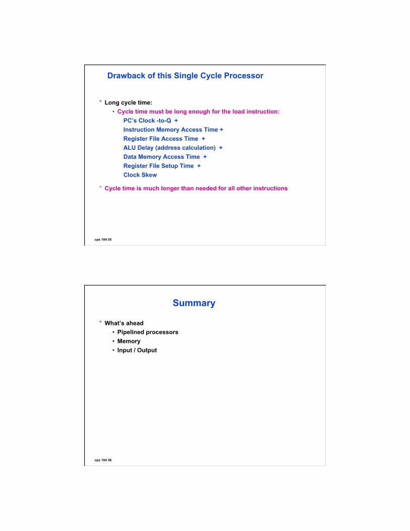
cps 104 55
Drawback of this Single Cycle Processor
° Long cycle time: • Cycle time must be long enough for the load instruction:
PC’s Clock -to-Q + Instruction Memory Access Time + Register File Access Time + ALU Delay (address calculation) + Data Memory Access Time + Register File Setup Time + Clock Skew
° Cycle time is much longer than needed for all other instructions
cps 104 56
Summary
° What’s ahead • Pipelined processors • Memory • Input / Output