minimal external components smart rf wireless ... - bascom- · pdf file3 at86rf401...
TRANSCRIPT

1424F–RKE–12/03
Smart RFWireless DataMicrotransmitter
AT86RF401
Features• RF Frequency Range of 264–456 MHz• 6 dBm RF Output into Matched Antenna• RF Output Power Adjustable over 36 dB with 1 dB Resolution• Phase-locked Loop (PLL) Based Frequency Synthesizer• Supports OOK Modulation• Data Bandwidth of Up to 10 Kbps Manchester• 2-volt Operation• 8-bit AVR RISC Microcontroller Core• Minimal External Components• Space-saving 20-lead TSSOP• 2 KB (1K x 16) of Flash Program Memory • 128 Bytes of EEPROM• 128 Bytes of SRAM• In-system Programmable Data and Program Memory• Six I/Os (Serial I/F, LED Drive Outputs, Button Input Interrupts) • Low Battery Detect and Brown-out Protection• Software Fine-tuning of VCO Tank Circuit
Applications• Remote Keyless Entry (RKE) Transmitters• Wireless Security Systems• Home Applicance Control (Lighting Control, Ceiling Fans)• Radio Remote Control (Hobby, Toys)• Garage Door Openers• Wireless PC Peripherals (Keyboard, Mouse)• Telemetry (Tire Pressure, Utility Meter, Asset Tracking)
DescriptionThe Atmel AT86RF401 Smart RF Microtransmitter is a highly integrated, low-cost RFtransmitter, combined with an AVR RISC microcontroller. It requires only a crystal, asingle LiMnO2 coin cell (CR2032 or similar), three capacitors, an inductor and a tuned-loop antenna to implement a complete on-off keyed (OOF) wireless RF datatransmitter.
Figure 1. Block Diagram
PHASEDETECTOROSCILLATOR
LOOPFILTER
VCO
PRESCALER÷ 24
RFAMP
LOO
P F
IL
CLOCK
RESET
WATCHDOG
LOW-VOLTAGE DETECT
BROWN-OUT PROTECT
AVR RISC µC2 KB Flash Program Memory
128 Bytes EEPROM Data Memory
L1 L2
DATA GAINTRIM
POWER
SUPPLY
SUPERVISOR
XTAL/CLK
XTALB
AVDD
AGND
ANT
ANTB
B+
DV
DD
DG
ND
IO5
IO4
IO3
SC
K/IO
2
SD
O/IO
1
SD
I/IO
0
RE
SE
TB
In-system programmable, nonvolatile Flash program memory and EEPROM data stor-age make possible rapid time-to-market and lower inventory costs.
In-system programmable, nonvolatile Flash program memory and EEPROM data stor-age make possible rapid time-to-market and lower inventory costs.In-systemprogrammable, nonvolatile Flash program memory and EEPROM data storage makepossible rapid time-to-market and lower inventory costs.Static current consumption iskept to a minimum with an ultra-low current shutdown mode. Normal operation resumeswhen a button is pressed. This activates the crystal oscillator circuit that serves as theclock for the AVR microcontroller.
The RF carrier is synthesized utilizing an on-board Voltage Controlled Oscillator (VCO).Optimal tuning of the VCO is maintained over component tolerance through the use of asoftware-controlled switched capacitor array. Its accuracy is maintained with a PLLdetector that compares the crystal oscillator to a frequency-scaled version (divided by24) of the RF carrier. The resulting error signal adjusts the VCO to produce a very stableRF carrier.
An interrupt-based bit-timer structure, integral to the AVR microcontroller, simplifies theimplementation of user-specific, data-bit encoding routines, such as PWM or Manches-ter, for modulating the RF carrier. Thirty-six dB of RF power output control is available tothe user in 1 dB steps and is addressable in software. The RF signal output is placed dif-ferentially on a tuned-loop antenna, which may be realized as a counterspread coppertrace on a PCB.
The AT86RF401 is fabricated in Atmel’s 0.6 µm Mixed Signal CMOS + EEPROM pro-cess, enabling true system-level integration (SLI).
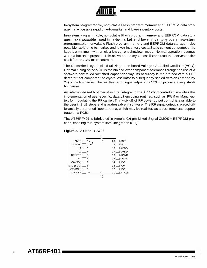
Figure 2. 20-lead TSSOP
12345678910
ANTBLOOPFIL
L1L2
RESETBN/C
I/O0 (SDI)I/O1 (SDO)I/O2 (SCK)XTAL/CLK
20191817161514131211
ANTN/CAVDDDVDDAGNDDGNDI/O5I/O4I/O3XTALB
2 AT86RF4011424F–RKE–12/03
AT86RF401
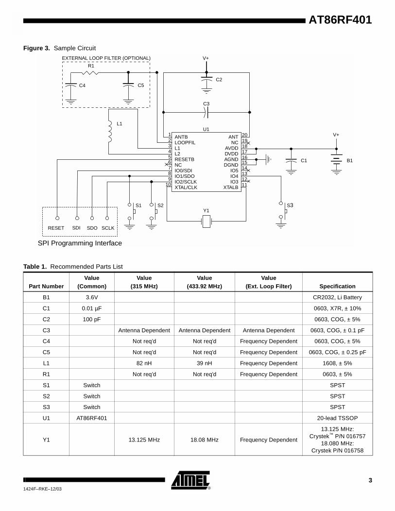
Figure 3. Sample Circuit
Table 1. Recommended Parts List
Part NumberValue
(Common)Value
(315 MHz)Value
(433.92 MHz)Value
(Ext. Loop Filter) Specification
B1 3.6V CR2032, Li Battery
C1 0.01 µF 0603, X7R, ± 10%
C2 100 pF 0603, COG, ± 5%
C3 Antenna Dependent Antenna Dependent Antenna Dependent 0603, COG, ± 0.1 pF
C4 Not req’d Not req’d Frequency Dependent 0603, COG, ± 5%
C5 Not req’d Not req’d Frequency Dependent 0603, COG, ± 0.25 pF
L1 82 nH 39 nH Frequency Dependent 1608, ± 5%
R1 Not req’d Not req’d Frequency Dependent 0603, ± 5%
S1 Switch SPST
S2 Switch SPST
S3 Switch SPST
U1 AT86RF401 20-lead TSSOP
Y1 13.125 MHz 18.08 MHz Frequency Dependent
13.125 MHz:Crystek™ P/N 016757
18.080 MHz:Crystek P/N 016758
ANTBLOOPFILL1L2RESETBNCIO0/SDIIO1/SDOIO2/SCLKXTAL/CLK
ANTNC
AVDDDVDDAGNDDGND
IO5IO4IO3
XTALB
S1 S2 S3Y1
RESET SDOSDI SCLK
U1
V+
C3
123456789
10
20191817161514131211
R1
C4 C5
V+
C2
C1 B1
SPI Programming Interface
L1
EXTERNAL LOOP FILTER (OPTIONAL)
31424F–RKE–12/03

Table 2. Pin Descriptions – 20-lead TSSOP
Symbol Pin Description
ANTB 1 Differential Antenna Output
LOOPFIL 2External VCO Loop-filter Connection.VVCO is the VCO control voltage.
L1 3External VCO Inductor Connection.VVCO is the VCO control voltage.
L2 4External VCO Inductor Connection.VVCO is the VCO control voltage.
1 20
10 mA
VDD VDD
VVCO
2
43
VDD VDD
VVCO
2
43
VDD VDD
VVDD
2
43
4 AT86RF4011424F–RKE–12/03

AT86RF401
RESETB 5
SPI Reset Input: A “low” on this pin resets the device and puts the part into SPI mode. A logic-high on this pin causes the device to execute its program if the VDD is above the brown-out voltage level.
NC 6 No Connect. Float Pin.
I/O0 (SDI) 7SPI Data In/Input/Output 0: General-purpose I/O and button input. In SPI mode, this pin serves as SDI (Serial Data Input).
I/O1 (SDO) 8SPI Data Out/Input/Output 1: General-purpose I/O and button input. In SPI mode, this pin serves as SDO (Serial Data Output).
I/O2 (SCK) 9SPI Clock/Input/Output 2: General-purpose I/O and button input. In SPI mode, this pin serves as SCK (SPI Clock Input).
XTAL/CLK 10Crystal/Clock Input: Input to the inverting oscillator amplifier and input to the internal clock operating circuit. This pin may be driven externally for test purposes.
Table 2. Pin Descriptions – 20-lead TSSOP (Continued)
VDD
35 k Ω5
To AVR
VDD VDD
Data
nable−
Data
Enable
735 k Ω
To AVR
VDD VDD
Data
Enable−
Data
Enable
835 k Ω
To AVR
VDD VDD
Data
Enable−
Data
Enable
935 k Ω
To AVR
40 pF
40 pF
10
11
51424F–RKE–12/03
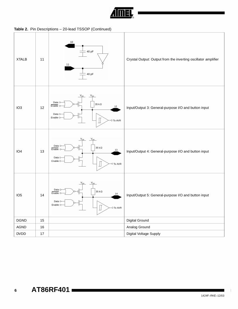
XTALB 11 Crystal Output: Output from the inverting oscillator amplifier
IO3 12 Input/Output 3: General-purpose I/O and button input
IO4 13 Input/Output 4: General-purpose I/O and button input
IO5 14 Input/Output 5: General-purpose I/O and button input
DGND 15 Digital Ground
AGND 16 Analog Ground
DVDD 17 Digital Voltage Supply
Table 2. Pin Descriptions – 20-lead TSSOP (Continued)
40 pF
40 pF
10
11
VDD VDD
Data
Enable
Data
Enable
1235 k Ω
To AVR
VDD VDD
Data
Enable
Data
Enable
1335 k Ω
To AVR
VDD VDD
Data
Enable
Data
Enable
1435 k Ω
To AVR
6 AT86RF4011424F–RKE–12/03

AT86RF401
AVDD 18 Analog Voltage Supply
N/C 19 No Connect – Float Pin
ANT 20 Differential Antenna Output
Table 2. Pin Descriptions – 20-lead TSSOP (Continued)
1 20
10 mA
71424F–RKE–12/03

Absolute Maximum Ratings*Antenna Voltage (Pins 1, 20) ......................................−1V to 10V *NOTICE: Stresses beyond those listed under “Absolute
Maximum Ratings” may cause permanent dam-age to the device. This is a stress rating only; functional operation of the device at these or other conditions beyond those indicated in the operational sections of this specification is not implied. Exposure to absolute maximum rating conditions for extended periods may affect device reliability.
Operating Temperature........................................−40°C to +85°C
Storage Temperature (without bias) ................−55°C to +125°C
Voltage on VDD with respect to ground ............................. 6.0V
Voltage on Pins 2–19 (TSSOP 20) ................ −0.1 to VDD +0.3V
Table 3. DC CharacteristicsVDD = 3.3V; fXTAL = 13.125 MHz; fAVR = fXTAL ÷ 16; TA = 25°C unless otherwise specified.
Symbol Parameter Conditions Min Typ Max Unit
Supply
VDD Supply Voltage 2.0 3.3 5.0 V
IDD
Standby Current (off)VDD = 3.3V
TA = 25°C– 0.1 0.5 µA
AVR Active – 3.4 – mA
Frequency Synthesizer + AVR Active – 14.3 – mA
Transmit (FS, AVR and Power Amp active) CW modulation – 23.2 – mA
Digital Inputs (SDI, SCK, RESETB, IOx)
VIH High-level Input Voltage 0.8* VDD – VDD V
VIL Low-level Input Voltage 0 – 0.2* VDD V
IIH High-level Input Current VIH = VDD , VDD = 5.0V – – 1 µA
IIL Low-level Input Current VIL = 0V, VDD = 5.0V −140 – – µA
Digital Outputs (SDO, IOx)
VOH High-level Output Voltage IOH = −500 µA VDD −0.4 – – V
VOL Low-level Output Voltage IOL= 2 mA – – 0.4 V
Microcontroller/System
tTX Time from Button Wake-up to RF Outputs Active – 0.5 1.0 ms
fAVR AVR Clock Frequency – – 1.25 MHz
EELIFE EEPROM Retention
Initial programming conditions:
VDD = 3.3V ± 10%
Temp = 25°C ± 10%
– – 10 years
EECYCLES EEPROM Write/Erase Endurance2.0V ≤ VDD ≤ 5.0V
−40°C ≤ Temp ≤ 85°C
– – 100,000 cycles
8 AT86RF4011424F–RKE–12/03

AT86RF401
Note: 1. Characterized but not guaranteed by test due to dependency on PCB trace antenna
Functional Description
The complete circuit consists of the following functional blocks.
Transmitter
Crystal Oscillator The crystal oscillator circuit is designed to work with crystals with fundamental frequen-cies between 11 and 19 MHz. Forty pF of internal capacitance is connected betweeneach of the crystal input pins and (chip) ground. Alternatively, an external clock can beused for these functions.
This circuit provides the master clock for the entire chip. A programmable divider is usedto provide the AVR system clock.
Radio Frequency Power Amplifier
The RF power amplifier generates a differential output suitable for driving an off-chiptuned-loop antenna from the PLL output. The PLL output signal is gated using on-offkeyed (OOK) modulation before transmission. It is used as the RF carrier frequency forthe transmitted data stream. The amplifier can be configured via software to reduce thepower output by 36 dB (with 1 dB resolution).
Frequency Synthesizer The frequency synthesizer utilizes a PLL, which consists of a phase detector, a ÷24prescaler, an on-chip loop filter and an integrated VCO. The VCO output is bufferedprior to the output amplifier. The output frequency is 24 times the crystal frequency. Tooffset component tolerance, a switched capacitor array is connected between pins 3and 4 of the VCO. Thirty-two discrete steps of capacitance are available to tune theVCO control voltage. An internal window comparator monitors the magnitude of the tun-ing voltage and is used by the AVR core to determine the optimal tuning configuration.
Lock Detector The lock detection block provides an indication of the state of the phase lock loop (PLL).Lock condition is determined by counting the number of cycle slips in a given time
Table 4. Analog/RF Specs
VDD = 3.3V; fXTAL = 13.125 MHz; fAVR = fXTAL ÷ 16; TA = 25°C unless otherwise specified.
Symbol Parameter Conditions Min Typ Max Unit
RF Amplifier
IPA Power Amp Output Current Transmitting (RF “ON”), 0 dB Attenuation – 8.6 – mA
PCTLRANGE Power Control Range – 36 – dB
PCTLRES Power Control Resolution – 1 – dB
Crystal Oscillator
fOSC Oscillation Frequency Range 11 – 19 MHz
Frequency Synthesizer/PLL
FOUT Output Frequency Range 264 – 456 MHz
PHARM1 Harmonics
I/O Pins Static during RF Transmission Using PCB Trace Antenna
– −60 – dBc
fMOD OOK Modulation Data Rate Using Manchester Data Bit Encoding – – 10 Kbps
91424F–RKE–12/03

period. A number of registers are available to adjust the performance of the lock detec-tor. These include lock delay and unlock delay timers as well as a cycle slip counter.
Bandgap Reference The device uses a 1.2V (nominal) bandgap reference generator to provide consistentperformance over a wide range of input supply voltages. This reference voltage is usedthroughout the device.
Brown-out Protection/Low Battery Detection
The brown-out protection and low battery detection functions consist of a voltage refer-ence, a sampling block and an autozero comparator. The circuit’s primary operatingmode is brown-out protection.
Brown-out Protection The brown-out protection circuit detects when the level of VDD drops below the minimumvoltage that guarantees proper operation. The brown-out voltage for this device is typi-cally 1.8 volts.
If a brown-out occurs, the device enters a reset state. It stays in this state until either ofthe following occurs:
• The level of VDD increases ~0.1–0.2 volts above the brown-out voltage. This causes the device to enter a warm reboot state.
• The level of VDD drops to ~0 volts, then increases above the POR level. This places the device into the “cold start” mode of operation, identical to battery insertion.
Low Battery Detection The low battery detection feature allows the programmer to select a voltage threshold(1.5–2.7 volts) for VDD at which a warning flag is issued to the user. For example, thiswarning may be utilized to activate an I/O port or to change the transmitted message.
Additionally, the programmer has the option of defining the amount of hysteresis on thisthreshold. More detail can be found in register descriptions for I/O Enable (IO_ENAB,$30, page 39) and Battery Low Configuration (BL_CONFIG, $35, page 42).
10 AT86RF4011424F–RKE–12/03
AT86RF401
Bit Timer A hardware assist has been included in the AT86RF401 to make transmission of dataeasier. Keying of the transmitter is timed by this logic, and interrupts are generatedwhen data is needed by the timer or when transmission is complete. The timer also sup-ports code that uses polling instead of interrupts. Using polling instead of interrupts mayfacilitate higher bit rates. Additionally, this timer may be used to time pulses arriving atthe I/O3 pin. This enables the AT86RF401 to be used to decode the signal detected byan external receiver chip. For additional information on how to implement the bit timer,see AT86RF401 Bit Timer Application Note, available at www.atmel.com.
Bit Timer in Transmit Mode Bit coding is done by the AVR before data is sent to the bit timer. Bit timing is controlledby the count value in the Bit Timer Count (BTCNT) register and the two most significantbits in the Bit Timer Control Register (BTCR). Generally the time of each bit is:
where Pxx is the period of each time slot and countval is the counter value in the BTCNTand BTCR registers. P is the AVR clock period that is set in the PWR_CTL register.countval = BTCR[7:6], BTCNT[7:0].
There are two interrupts associated with transmit mode:
1. Transmit Buffer Empty Interrupt: This vectors to address 0x04. Flag 0 is set, and, if enabled, this interrupt is generated when the timer removes the value from the DATA bit in the BTCR. This interrupt service routine should load the next transmit bit into the DATA bit in the BTCR.
2. TXDONE Interrupt: This vectors to address 0x02. Flag 2 is set, and, if enabled, an interrupt is generated when the counter has counted down to zero and the buffer is empty. This indicates that the transmission is complete. This interrupt service routine should turn off the transmitter and turn off the bit timer using the mode bits.
Bit Timer in Receive Mode When put into receive mode, the bit timer times pulses arriving at the I/O3 pin. Whenenabled, the counter counts up from zero and places that value in the BTCNT registerwhen an edge occurs. If the edge is rising, the DATA bit in the BTCR is set. If the edgeis falling, the DATA bit in the BTCR is reset. This mode may be used to decode signalsfrom a receiver chip easily.
Bit Timer in Generic Timer/Counter Mode
The bit timer may be used as a generic timer by not allowing it to key off the transmitter.An interrupt is generated after the amount of time dictated by the count value.
Pxx P countval 1+( )×=
111424F–RKE–12/03

Watchdog Timer When enabling the watchdog timer, the status of the watchdog time is unknown. Theuser is advised to execute a WDR instruction before enabling the watchdog. Otherwise,the device might get reset before the first WDR after enabling is reached. To prevent theunintentional disabling of the watchdog, a special turn-off procedure must be followedwhen the watchdog is disabled. Refer to the description of the Watchdog Timer ControlRegister on page 38 for details (see Register $22 in I/O Memory). The watchdog timerprescaler determines the number of system clocks that occur before the watchdog resetis asserted. The system clock is determined by Bits[7:5] of the AVR_CONFIG register.
Reset and Interrupt Handling
The AT86RF401 Reset and Interrupt vectors are defined in Table 5. The I-bit in the sta-tus register must be set to enable the interrupts.
The most typical and general program setup for the Reset and Interrupt VectorAddresses are:
Reset Sources The AT86RF401 has several sources of reset:
• Power-on Reset: The device is reset when the supply voltage is applied between the VDD and GND pins. There are 106 cycles of delay between Power-on Reset occurring and the part becoming active. This is to ensure that the power is stable.
• External Reset: The device is reset when a logic low level is present on the RESETB pin. This resets all I/O Registers and puts the part into SPI mode. The I/O Registers may be read and written by the SPI interface after two AVR System Clocks.
• Watchdog Reset: This is similar to power-on reset but is caused by the watchdog timer and does not have a 106 cycle delay prior to becoming active.
• Brown-out Reset: This is caused by the battery voltage dropping below the Brown-out Threshold voltage trip point.
• Button Reset (software reset): The part is placed into a special reset state by software. The part is released from reset when a properly configured button is activated, and the part is not in external reset or brown-out reset. In the button reset state, most I/O registers are not reset, and there is no time delay before becoming active.
Table 5. Reset and Interrupt Vectors
Vector Number
Program Address Source Interrupt Definition
1 $000 RESETB, Watchdog, Buttons Hardware Pin or Watchdog or Button Reset
2 $002 Transmission Done (TXDONE) Bit Timer Flag 2 Interrupt
4 $004 Transmit Buffer Empty Bit Timer Flag 0 Interrupt
Address Labels Code Comments
$000 jmp RESET ; Reset handler
$002 jmp BT_F2_ISR ; Bit timer flag 2 interrupt service routine
$004 jmp BT_F0_ISR ; Bit timer flag 0 interrupt service routine
$006 MAIN: <instr> xxx ; Main program start
… … … …
12 AT86RF4011424F–RKE–12/03

AT86RF401
During power-on reset and watchdog reset, all I/O registers are set to their initial values,and the program starts execution from address $000. Note: The instruction placed in address $000 must be an RJMP (relative jump) instruction or a
JMP (absolute jump) to the reset handling routine. If an RJMP or JMP instruction is notpresent at address $000, the part is placed into a “no program” reset state. This is to pro-tect the part from fetching instructions when no program is present.
Interrupt Response Time The interrupt execution response for all the enabled AVR interrupts is a minimum of fourclock cycles. After the four clock cycles, the program vector address for the actual inter-rupt handling routine is executed. During this four clock cycle period, the ProgramCounter is pushed onto the stack. The vector is a jump to the interrupt routine, and thisjump takes two clock cycles. If an interrupt occurs during execution of a multi-cycleinstruction, this instruction is completed before the interrupt is served.
A return from an interrupt handling routine takes four clock cycles. During these fourclock cycles, the Program Counter is popped back from the stack. When AVR exits froman interrupt, it will always return to the main program and execute one more instructionbefore any pending interrupt is served.Note: The Status Register (SREG) is not saved by the AVR hardware. This must be performed
by user software when required.
Memory Programming
Program Memory Lock Bits
The AT86RF401 microtransmitter provides two lock bits that can be left unprogrammed(“1”) or can be programmed (“0”) to obtain the additional features listed in Table 6.
Note: The lock bits can only be erased with the Chip Erase operation.
In-system Flash and EEPROM
The AT86RF401 offers 2 Kbytes (1K x 16) of in-system reprogrammable Flash programmemory and 128 bytes of EEPROM data memory. This memory can be programmedserially via the SPI interface.
SPI Interface Both the program and data memory arrays can be programmed using the serial SPI buswhile RESETB is pulled to GND. The serial interface consists of pins SCK, SDI (input)and SDO (output).
When programming, an auto-erase cycle is built into the self-timed programming opera-tion, and there is no need to first execute the Chip Erase instruction. The Chip Eraseoperation sets every memory location in the EEPROM array to $FF.
Either an external system clock is supplied at pin XTAL/CLK or a crystal needs to beconnected across pins XTAL/CLK and XTALB. The minimum low and high periods forthe serial clock (SCK) input are defined as follows:
Low: 4 XTAL Clock Cycles High: 16 XTAL Clock Cycles
Table 6. Lock Bit Protection Modes
Program Lock Bits
Protection TypeMod
eLB1 LB2
1 1 1 No program lock features
2 0 1Further serial (SPI) programming of the EEPROM is disabled (both program and data memory).
3 0 0 Same as mode 2, but Verify is also disabled
131424F–RKE–12/03

Serial Programming Algorithm
Refer to Figure 4 (page 15), Figure 5 (page 16) and Figure 6 (page 17). To program andverify the AT86RF401 in the serial programming mode, the following sequence isrecommended.
Power-up Sequence:
1. Apply power between VDD and GND while RESETB and SCK are set to “0”. If a crystal is not connected across pins XTAL and XTALB, apply a clock signal to the XTAL pin. If the programmer can not guarantee that SCK is held low during power-up, RESETB must be given a positive pulse after SCK has been set to “0”.
2. Wait for at least 20 ms and enable serial programming by sending the Program-ming Enable instruction to pin SDI. This must occur prior to any program/erase operations.
3. If a chip erase is performed, wait 4 ms, give RESETB a positive pulse and start over again from Step 2.
4. The array is programmed one byte at a time by supplying the address and data together with the appropriate Write instruction. The memory location is first auto-matically erased before new data is written. The next byte can be written after 4 ms.
5. Any memory location can be verified by using the Read instruction, which returns the content at the selected address at serial output SDO.
6. At the end of the programming session, RESETB must be set high to commence normal operation.
Signature Bytes All Atmel microcontrollers have a three-byte signature code that identifies the device.For the AT86RF401, the signature bytes are:
• 0x000: 0x1E (indicates manufactured by Atmel)
• 0x001: 0x91 (indicates 2 Kbytes Flash program memory)
• 0x002: 0x81 (indicates AT86RF401 when 0x001 is 0x91)
14 AT86RF4011424F–RKE–12/03

AT86RF401
Data EEPROM Access from the AVR
Note: a = address high bitsb = address low bitsH = 0: Low byte, 1: High byteo = data outi = data inx = don’t care1= lock bit 12= lock bit 2
Figure 4. Serial Programming and Verify
Notes: 1. When writing, data is clocked on the rising edge of CLK.2. When reading, data is clocked on the falling edge of CLK. See Figure 5 for an
explanation.
Table 7. AT86RF401 Serial Programming Instruction Set
Instruction
Instruction Format
OperationByte 1 Byte 2 Byte 3 Byte 4
Programming Enable
1010 1100 0101 0011 xxxx xxxx xxxx xxxxEnable Serial Programming after RESETB goes low.
Chip Erase 1010 1100 100x xxxx xxxx xxxx xxxx xxxx Chip erase EEPROM
Read ProgramMemory
0010 H000 0000 00aa bbbb bbbb oooo ooooRead H (high or low) data o from Program memory at word address a:b
Write ProgramMemory
0100 H000 0000 00aa bbbb bbbb iiii iiiiWrite H (high or low) data i to Program memory at word address a:b
Read EEPROM Memory
1010 0000 0000 0000 xbbb bbbb oooo ooooRead data o from EEPROM memory at address b
Write EEPROM Memory
1100 0000 0000 0000 xbbb bbbb iiii iiiiWrite data i to EEPROM memory at address b
Write Lock Bits 1010 1100 111x x21x xxxx xxxx xxxx xxxxWrite lock bits. Set bits 21 = “0” to program lock bits.
I/O Read 10110000 0000 0000 00bbbbbb oooo oooo Read data 0 from I/O memory address b
I/O Write 11010000 0000 0000 00bbbbbb iiii iiii Write data i to I/O memory address b
Read Signature Byte 0011 0000 000x xxxx xxxx xxbb oooo oooo
BAT
SCK
SDO
SDI
RESETB
XTAL
XTALB
2.0–3.5V
CLOCK IN
DATA OUT
INSTR. IN, DATA IN
GND
6 to 20 MHz
AT86RF401
151424F–RKE–12/03

Figure 5. Serial Programming Waveforms
Note: This device includes an integrated 128-byte EEPROM, which is accessed by three registers located in the I/O memory space.These are the DEECR, DEEDR and DEEAR registers. For more information, refer to I/O Register Description.
AVR Core
Architectural Overview The fast-access register file concept contains 32 x 8-bit general-purpose working regis-ters with a single clock cycle access time. This means that during one single clock cycle,one Arithmetic Logic Unit (ALU) operation is executed. Two operands are output fromthe register file, the operation is executed, and the result is stored back in the registerfile in one clock cycle.
Six of the 32 registers can be used as three 16-bit indirect address register pointers forData Space addressing, enabling efficient address calculations. One of the threeaddress pointers is also used as the address pointer for look-up tables in Flash programmemory. These added function registers are the 16-bit X-register, Y-register and Z-register.
The ALU supports arithmetic and logic operations between registers or between a con-stant and a register. Single register operations are also executed in the ALU. Figure 6shows the AT86RF401 AVR architecture.
In addition to the register operation, the conventional memory addressing modes can beused on the register file as well. This is enabled by the fact that the register file isassigned the 32 lowest data space addresses ($00–$1F), allowing them to be accessedas though they were ordinary memory locations.
The I/O memory space contains 64 addresses for CPU peripheral functions as ControlRegisters, Timer/Counters, A/D converters and other I/O functions. The I/O Memory canbe accessed directly or as the Data Space locations following those of the register file,$20–$5F.
SERIAL DATA INPUT (SDI)
SERIAL DATA OUTPUT (SDO)
SERIAL CLOCK INPUT (SCK)
MSB
MSB LSB
LSB
16 AT86RF4011424F–RKE–12/03

AT86RF401
Figure 6. AVR Core Architecture
The AVR uses a Harvard architecture concept, with separate memories and buses forprogram and data. The program memory is executed with a two-stage pipeline. Whileone instruction is being executed, the next instruction is prefetched from the programmemory. This concept enables instructions to be executed in every clock cycle. The pro-gram memory is in-system, reprogrammable Flash memory.
With the jump and call instructions, the whole 1K word address space is directlyaccessed. Most AVR instructions have a single 16-bit word format. Every programmemory address contains a 16- or 32-bit instruction.
During interrupts and subroutine calls, the return address program counter (PC) isstored on the stack. The stack is effectively allocated in the general data SRAM, andconsequently the stack size is only limited by the total SRAM size and the usage of theSRAM. All user programs must initialize the SP in the reset routine (before subroutinesor interrupts are executed). The 7-bit stack pointer SP is read/write accessible in the I/Ospace.
The 128-byte data SRAM can be easily accessed through the five different addressingmodes supported in the AVR architecture.
The memory spaces in the AVR architecture are all linear and regular memory maps.
1K x 16ProgramMemory
InstructionRegister
InstructionDecoder
ProgramCounter
Control Lines
32 x 8GeneralPurpose
Registers
ALU
Statusand Control Bit Timer
SPI Unit
ProgrammableClock Divider
128 x 8EEPROM
Data Bus 8-bit
Brown-out/LowBattery Detector
128 x 8Data
SRAMD
irect
Add
ress
ing
Indi
rect
Add
ress
ing
RFTransmitter
WatchdogTimer
6 I/O Lines
171424F–RKE–12/03

A flexible interrupt module has its control registers in the I/O space with an additionalglobal interrupt enable bit in the status register. All interrupts have a separate interruptvector in the interrupt vector table at the beginning of the program memory. The inter-rupts have priority in accordance with their interrupt vector position; the lower theinterrupt vector address, the higher the priority.
Figure 7. Memory Maps
$000
$3FF
Program Memory
Application Flash Section
18 AT86RF4011424F–RKE–12/03

AT86RF401
General-purpose Register File
Figure 8 shows the structure of the 32 general-purpose working registers in the CPU.
Figure 8. AVR CPU General-purpose Working Registers
All the register operating instructions in the instruction set have direct and single cycleaccess to all registers. The only exception is the five constant arithmetic and logicinstructions (SBCI, SUBI, CPI, ANDI and ORI) between a constant and a register, andthe LDI instruction for load immediate constant data. These instructions apply to thesecond half of the registers in the register file, R16...R31. The general SBC, SUB, CP,AND and OR and all other operations between two registers or on a single register applyto the entire register file.
As shown in Figure 9, each register is also assigned a data memory address, mappingthe registers directly into the first 32 locations of the user data space. Although not beingphysically implemented as SRAM locations, this memory organization provides greatflexibility in access of the registers, as the X, Y and Z registers can be set to index anyregister in the file.
7 0 Addr.
R0 $00
R1 $01
R2 $02
…
R13 $0D
R14 $0E
R15 $0F
R16 $10
R17 $11
…
R26 $1A X-register low byte
R27 $1B X-register high byte
R28 $1C Y-register low byte
R29 $1D Y-register high byte
R30 $1E Z-register low byte
R31 $1F Z-register high byte
191424F–RKE–12/03

The X, Y and Z Registers The registers R26...R31 have some added functions to their general-purpose usage.These registers are address pointers for indirect addressing of the data space. Thethree indirect address registers X, Y and Z are defined as shown in Figure 9.
Figure 9. The X, Y and Z Registers
In the different addressing modes, these address registers have functions as fixed dis-placement, automatic increment and decrement (see the descriptions for the differentinstructions).
Arithmetic Logic Unit (ALU)
The high-performance AVR ALU operates in direct connection with all the 32 general-purpose working registers. Within a single clock cycle, ALU operations between regis-ters in the register file are executed. The ALU operations are divided into three maincategories: arithmetic, logical and bit-functions. The multiplier is not present in this ver-sion of the core. Therefore, the MUL instruction is not supported.
In-system Self-programmable Flash Program Memory
The AT86RF401 contains 2 Kbytes of on-chip Flash memory for program storage. Sinceall instructions are 16- or 32-bit words, the Flash is organized as 1K x 16.
The Flash memory has an endurance of at least 1000 write/erase cycles. The PC is 10bits wide, thus addressing the 1024 program memory locations. See the Memory Pro-gramming section (page 13) for a detailed description on Flash data serial downloading.
Constant tables can be allocated within the entire program memory address space (seeTable 22, Instruction Set, page 45).
15 XH XL 0
X Register 70 0 7 0
R27 ($1B) R26 ($1A)
15 YH YL 0
Y Register 70 0 7 0
R29 ($1D) R28 ($1C)
15 ZH ZL 0
Z Register 70 0 7 0
R30 ($1F) R31 ($1E)
20 AT86RF4011424F–RKE–12/03
AT86RF401
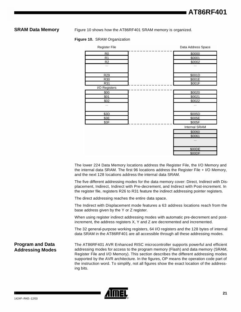
SRAM Data Memory Figure 10 shows how the AT86RF401 SRAM memory is organized.
Figure 10. SRAM Organization
The lower 224 Data Memory locations address the Register File, the I/O Memory andthe internal data SRAM. The first 96 locations address the Register File + I/O Memory,and the next 128 locations address the internal data SRAM.
The five different addressing modes for the data memory cover: Direct, Indirect with Dis-placement, Indirect, Indirect with Pre-decrement, and Indirect with Post-increment. Inthe register file, registers R26 to R31 feature the indirect addressing pointer registers.
The direct addressing reaches the entire data space.
The Indirect with Displacement mode features a 63 address locations reach from thebase address given by the Y or Z register.
When using register indirect addressing modes with automatic pre-decrement and post-increment, the address registers X, Y and Z are decremented and incremented.
The 32 general-purpose working registers, 64 I/O registers and the 128 bytes of internaldata SRAM in the AT86RF401 are all accessible through all these addressing modes.
Program and Data Addressing Modes
The AT86RF401 AVR Enhanced RISC microcontroller supports powerful and efficientaddressing modes for access to the program memory (Flash) and data memory (SRAM,Register File and I/O Memory). This section describes the different addressing modessupported by the AVR architecture. In the figures, OP means the operation code part ofthe instruction word. To simplify, not all figures show the exact location of the address-ing bits.
Register File
R0R1R2
R29R30R31
I/O Registers$00$01$02
...
$3D$3E$3F
...
$0000$0001$0002
$001D$001E$001F
$0020$0021$0022
...
$005D$005E$005F
...
Data Address Space
$0060$0061
$00DE$00DF
...
Internal SRAM
211424F–RKE–12/03
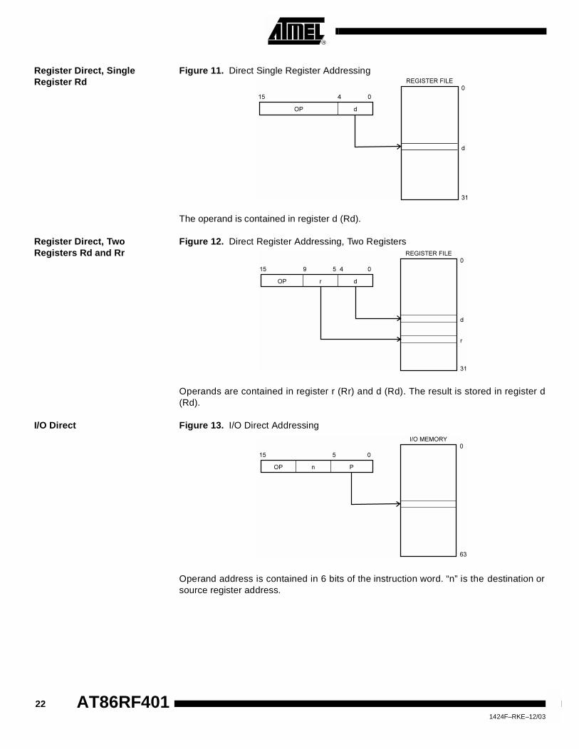
Register Direct, Single Register Rd
Figure 11. Direct Single Register Addressing
The operand is contained in register d (Rd).
Register Direct, TwoRegisters Rd and Rr
Figure 12. Direct Register Addressing, Two Registers
Operands are contained in register r (Rr) and d (Rd). The result is stored in register d(Rd).
I/O Direct Figure 13. I/O Direct Addressing
Operand address is contained in 6 bits of the instruction word. “n” is the destination orsource register address.
22 AT86RF4011424F–RKE–12/03

AT86RF401
Data Direct Figure 14. Direct Data Addressing
A 16-bit Data Address is contained in the 16 LSBs of a two-word instruction. Rd/Rrspecify the destination or source register.
Data Indirect with Displacement
Figure 15. Data Indirect with Displacement
Operand address is the result of the Y or Z register contents added to the address con-tained in 6 bits of the instruction word.
Data Indirect Figure 16. Data Indirect Addressing
Operand address is the contents of the X, Y or Z register.
OP Rr/Rd
1631
15 0
16 LSBs
$00
$DF
20 19
Data Space
Data Space$00
$DF
Y OR Z - REGISTER
OP an
0
05610
15
15
Data Space$0000
$DF
X, Y OR Z - REGISTER
015
231424F–RKE–12/03

Data Indirect withPre-decrement
Figure 17. Data Indirect Addressing with Pre-decrement
The X, Y or Z register is decremented before the operation. Operand address is thedecremented contents of the X, Y or Z register.
Data Indirect withPost-increment
Figure 18. Data Indirect Addressing with Post-increment
The X, Y or Z register is incremented after the operation. Operand address is the con-tent of the X, Y or Z register prior to incrementing.
Constant Addressing Using the LPM Instruction
Figure 19. Code Memory Constant Addressing
Constant byte address is specified by the Z register contents. The 10 MSBs select wordaddress (0–1K). For LPM, the LSB selects low byte if cleared (LSB = 0) or high byte ifset (LSB = 1).
Data Space$0000
$DF
X, Y OR Z - REGISTER
015
-1
Data Space$0000
$DF
X, Y OR Z - REGISTER
015
1
$3FF
24 AT86RF4011424F–RKE–12/03

AT86RF401
Indirect Program Addressing, IJMP and ICALL
Figure 20. Indirect Program Memory Addressing
Program execution continues at address contained by the Z register (i.e., the PC isloaded with the contents of the Z register).
Relative Program Addressing, RJMP and RCALL
Figure 21. Relative Program Memory Addressing
Program execution continues at address PC + k + 1. The relative address k is from−2048 to 2047.
$3FF
$3FF
1
251424F–RKE–12/03

EEPROM Data Memory The AT86RF401 contains 128 bytes of data EEPROM memory. It is organized as a sep-arate data space in which single bytes can be read and written. The access between theEEPROM and the CPU is described in the Memory Programming section (page 13).
Memory Access Times and Instruction Execution Timing
This section describes the general access timing concepts for instruction execution andinternal memory access.
The AVR CPU is driven by the System Clock Ø generated from the main oscillator forthe chip. A programmable clock divider generates this clock from the crystal oscillatorinput.
Figure 22 shows the parallel instruction fetches and instruction executions enabled bythe Harvard architecture and the fast-access register file concept. This is the basic pipe-lining concept to obtain up to 1 MIPS per MHz with the corresponding unique results forfunctions per cost, functions per clocks and functions per power unit.
Figure 22. The Parallel Instruction Fetches and Instruction Executions
Figure 23 shows the internal timing concept for the register file. In a single clock cycle,an ALU operation using two register operands is executed, and the result is stored backto the destination register.
Figure 23. Single Cycle ALU Operation
System Clock Ø
1st Instruction Fetch
1st Instruction Execute2nd Instruction Fetch
2nd Instruction Execute3rd Instruction Fetch
3rd Instruction Execute4th Instruction Fetch
T1 T2 T3 T4
System Clock Ø
Total Execution Time
Register Operands Fetch
ALU Operation Execute
Result Write Back
T1 T2 T3 T4
26 AT86RF4011424F–RKE–12/03
AT86RF401
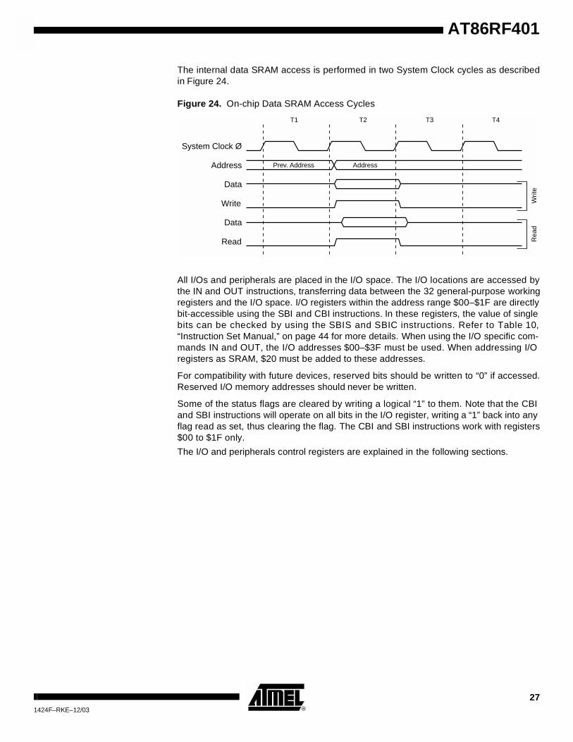
The internal data SRAM access is performed in two System Clock cycles as describedin Figure 24.
Figure 24. On-chip Data SRAM Access Cycles
All I/Os and peripherals are placed in the I/O space. The I/O locations are accessed bythe IN and OUT instructions, transferring data between the 32 general-purpose workingregisters and the I/O space. I/O registers within the address range $00–$1F are directlybit-accessible using the SBI and CBI instructions. In these registers, the value of singlebits can be checked by using the SBIS and SBIC instructions. Refer to Table 10,“Instruction Set Manual,” on page 44 for more details. When using the I/O specific com-mands IN and OUT, the I/O addresses $00–$3F must be used. When addressing I/Oregisters as SRAM, $20 must be added to these addresses.
For compatibility with future devices, reserved bits should be written to “0” if accessed.Reserved I/O memory addresses should never be written.
Some of the status flags are cleared by writing a logical “1” to them. Note that the CBIand SBI instructions will operate on all bits in the I/O register, writing a “1” back into anyflag read as set, thus clearing the flag. The CBI and SBI instructions work with registers$00 to $1F only.
The I/O and peripherals control registers are explained in the following sections.
System Clock Ø
Write
Read
Data
Data
Address Address
T1 T2 T3 T4
Prev. Address
Rea
dW
rite
271424F–RKE–12/03

I/O MemoryThe I/O space definition of the AT86RF401 is shown in Table 8 below.
Note: Reserved and unused locations are not shown in the table.
Table 8. AT86RF401 I/O Space Definitions
Address Hex Name Function
$3F SREG Status Register
$3E SPH Stack Pointer High Register (program to 0 x 00)
$3D SPL Stack Pointer Low Register
$35 BL_CONFIG Battery Low Configuration Register
$34 B_DET Button Detect Register
$33 AVR_CONFIG AVR Configuration Register
$32 IO_DATIN I/O DATA IN Register
$31 IO_DATOUT I/O DATA OUT Register
$30 IO_ENAB I/O Enable Register
$22 WDTCR Watchdog Timer Control Register
$21 BTCR Bit Timer Control Register
$20 BTCNT Bit Timer Count Register
$1E DEEAR Data EEPROM Address Register
$1D DEEDR Data EEPROM Data Register
$1C DEECR Data EEPROM Control Register
$17 LOCKDET2 Lock Detector Configuration Register 2
$16 VCOTUNE VCO Tuning Register
$14 PWR_ATTEN Power Attenuation Control Register
$12 TX_CNTL Transmitter Control Register
$10 LOCKDET1 Lock Detector Configuration Register 1
28 AT86RF4011424F–RKE–12/03
AT86RF401
I/O and Control Registers
The AT86RF401 I/Os and peripherals are placed in the I/O space. The various I/O loca-tions are accessed by the IN and OUT instructions transferring data between the 32general-purpose working registers and the I/O space. I/O registers within the addressrange $00–$1F are directly bit-accessible using the SBI and CBI instructions. In theseregisters, the value of single bits can be checked by using the SBIS and SBIC instruc-tions. Refer to Table 22 on page 45 for more details. The different I/O and peripheralscontrol registers are explained in the following sections.
Transmitter Control Register Descriptions
Lock Detector Configuration Register 1 – LOCKDET1
• Bits[7:5]
Reserved.
• Bit[4]: UPOK
If set high, this bit resets the unlock counter. The bit is level sensitive, and the unlockcounter will not count unless this bit is set to “0”. Leaving this bit high essentially dis-ables the unlock detector.
• Bit[3]: ENKO (Enable Key on Bit)
If set to “1”, the rising edge of TXK starts the blackout period, during which any cycleslips are ignored and do not affect the unlock circuit.
• Bit[2]: BOD (Black Out Disable)
When set high, cycle slips are counted immediately but only if LOCK is asserted high(TX_CNTL b[2]).
• Bits[1:0] CS[1:0]: Cycle Slip Counter
These two bits determine how many cycle slips are allowed before the LOCKDETECTsignal is set low. The cycle slips are not counted unless the blackout logic is either dis-abled or the blackout window has passed.
Table 9. Cycle Slip Counter Definition
Bit 7 6 5 4 3 2 1 0
$10 – – – UPOK ENKO BOD CS1 CS0
Read/Write R/W R/W R/W R/W R/W R/W R/W R/W
Initial Value 0 0 0 0 0 0 0 0
CS[1:0] Functionality
00 1 cycle slip causes unlock condition
01 2 cycle slips cause unlock condition
10 3 cycle slips cause unlock condition
11 4 cycle slips cause unlock condition
291424F–RKE–12/03

Transmit Control Register – TX_CNTL
• Bit[7:6]
Reserved.
• Bit[5]: TXE, Transmitter Enable
This bit, when set, turns on the phase locked loop (PLL) RF frequency synthesizer butshould not be used to modulate the RF carrier or excessive spurious noise may result.
• Bit[4]: TXK, Transmitter Key
This bit, when set, turns on the RF power amplifier. It should be used to modulate theRF carrier manually. This bit should be cleared when the bit timer is configured in trans-mit mode.
Figure 25. Modulation Control Logic
• Bit[3]
Reserved.
• Bit[2]: LOC, PLL Lock
This bit is set when the frequency synthesizer in the transmitter is locked. Typically, theprogrammer should test the status of this bit to insure the RF carrier is stable prior toturning on the RF power amplifier.
Power Attenuation Control Register – PWR_ATTEN
This register is used to select the power attenuation level. The total power attenuation isthe sum of the coarse attenuation and fine attenuation. As an example, to obtain 15 dBof attenuation, the coarse setting of 12 dB and fine setting of 3 dB would be selected. Toobtain 12 dB coarse attenuation, Bits[5:3] would be set to [010]. To obtain 3 dB of fineattentuation would require Bits[2:0] to be set to [011].
Note: Maximum RF output power occurs when Bits[5:0] = [000000].
• Bits[7:6]
Reserved
Bit 7 6 5 4 3 2 1 0
$12 – – TXE TXK – LOC – –
Read/Write R/W R/W R/W R/W R/W R R/W R/W
Initial Value 0 0 0 0 0 0 0 0
Bit Timer
TXK
ON/OFF
POWERAMPPLL RF
INRF
OUT
Bit 7 6 5 4 3 2 1 0
$14 – – PCC2 PCC1 PCC0 PCF2 PCF1 PCF0
Read/Write R/W R/W R/W R/W R/W R/W R/W R/W
Initial Value 0 0 0 0 0 0 0 0
30 AT86RF4011424F–RKE–12/03

AT86RF401
• Bits[5:3]: PCC, Power Control (coarse)
Attenuates the output power in 6 dB steps.
Table 10. Coarse Power Control Definition
• Bits[2:0]: PCF, Power Control (fine)
Attenuates the output power in 1 dB steps.
Table 11. Fine Power Control Definition
VCO Tuning Register 6 – VCOTUNE
Note: * These values are unknown at initial startup.
• Bits[4:0]: VCO Tuning Capacitor Array
This device requires the use of an external inductor to tune the VCO. Tolerance of theinductor, coupled with process variation of the device, can lead to variations in the tun-ing point of the VCO. A switched array of tuning capacitors has been added internally tothe device in order to “fine tune” the VCO. This capacitance is switched across pins 3and 4 (L1 and L2) of the device. The capacitor array is set by VCOTUNE[4:0] and iscomprised of the following switched capacitance levels:
PCC[5:3] Output Attenuation
000 0 dB
001 6 dB
010 12 dB
011 18 dB
100 24 dB
101 30 dB
110 Invalid
111 Invalid
PCF[2:0] Output Attenuation
000 0 dB
001 1 dB
010 2 dB
011 3 dB
100 4 dB
101 5 dB
110 Invalid
111 Invalid
Bit 7 6 5 4 3 2 1 0
$16 VCOVDET[1] VCOVDET[0] – VCOTUNE[4] VCOTUNE[3] VCOTUNE[2] VCOTUNE[1] VCOTUNE[0]
Read/Write R R R/W R/W R/W R/W R/W R/W
Initial Value * * 0 0 0 0 0 0
311424F–RKE–12/03

Table 12. VCO Tuning Capacitor Definition
VCOTUNE[4:0] Capacitance (pF)
00000 0
00001 0.03
00010 0.06
00011 0.09
00100 0.12
00101 0.15
00110 0.18
00111 0.21
01000 0.24
01001 0.27
01010 0.30
01011 0.33
01100 0.36
01101 0.39
01110 0.42
01111 0.45
10000 0.48
10001 0.51
10010 0.54
10011 0.57
10100 0.60
10101 0.63
10110 0.66
10111 0.69
11000 0.72
11001 0.75
11010 0.78
11011 0.81
11100 0.84
11101 0.87
11110 0.90
11111 0.93
32 AT86RF4011424F–RKE–12/03

AT86RF401
• Bits[7:6]: VCO Voltage Detector
The VCO Voltage Detector circuit monitors the level of the VCO control voltage. This cir-cuit, along with the VCO Switch Caps and the Lock Detect circuit, is intended for usewith a software algorithm to tune the VCO such that the VCO control voltage is centeredapproximately at 1.1V.
The Voltage Detector circuit consists of two comparators with fixed reference voltagesof V1 (lower reference voltage) and V2 (upper reference voltage). The VCO ControlVoltage is compared to these two reference voltages and generates the state tablelisted in Table 13. The state of these comparators is output to Bits 7 and 6 (Vcodet[1:0])of the VCOTUNE register.
Lock Detector Configuration Register 2 – LOCKDET2
• Bit[7]: EUD
A “1” enables the unlock detect logic.
• Bit[6]: LAT (Lock Always True)
Forces the lockdetect signal to “1” at the output of the lock detect circuitry. This may beuseful if the lock detect signal is not going high for some reason, and a power amp inter-lock has been implemented, and the user wishes to enable the power amp output stage.
Table 13. VCO Window Comparator States
VCOvdet[1:0] VCO Control Voltage
00Above lower comparator threshold and below upper comparator threshold. Control Voltage is within the valid window of operation.
01Below both thresholds. Control Voltage is outside the recommended window of operation.
10Above both thresholds. Control Voltage is outside the recommended window of operation.
11 Not a valid state.
Bit 7 6 5 4 3 2 1 0
$17 EUD LAT ULC[2] ULC[1] ULC[0] LC[2] LC[1] LC[0]
Read/Write R/W R/W R/W R/W R/W R/W R/W R/W
Initial Value 0 0 0 0 0 0 0 0
331424F–RKE–12/03

• Bit[5:3]: ULC[2:0]
The unlock count (ULC) bits count a certain number of reference clocks, after which theunlock detect circuit looks for a number of cycle slips determined by CS[1:0] beforemaking the loc detect signal go low. The ULC bits essentially control the blackout periodof the unlock detect circuit. The unlock counter is reset by the KEY signal rising (ifENKO is asserted), or by the LOC rising edge, or by the UPOK signal being set high.
Table 14. PLL Unlock Counter Definition
• Bits[2:0]: LC[2:0]
The Lock Count (LC) bits control a counter that, after a number of reference clocks,cause lock detect to go high. This counter will reset if a cycle slip or a reset signal occurs(which happens if TXE goes low), if an out-of-lock condition occurs, if the crystal oscilla-tor frequency is too low, or if the VCO feedback frequency is too low.
Table 15. PLL Lock Counter Definition
ULC[2:0]Number of REFClocks of Delay
000 8
001 16
010 32
011 64
100 128
101 256
110 512
111 1024
LC[2:0] Number of REF Clocks of Delay
000 8
001 16
010 32
011 64
100 128
101 256
110 512
111 1024
34 AT86RF4011424F–RKE–12/03
AT86RF401
EEPROM Control Register Descriptions
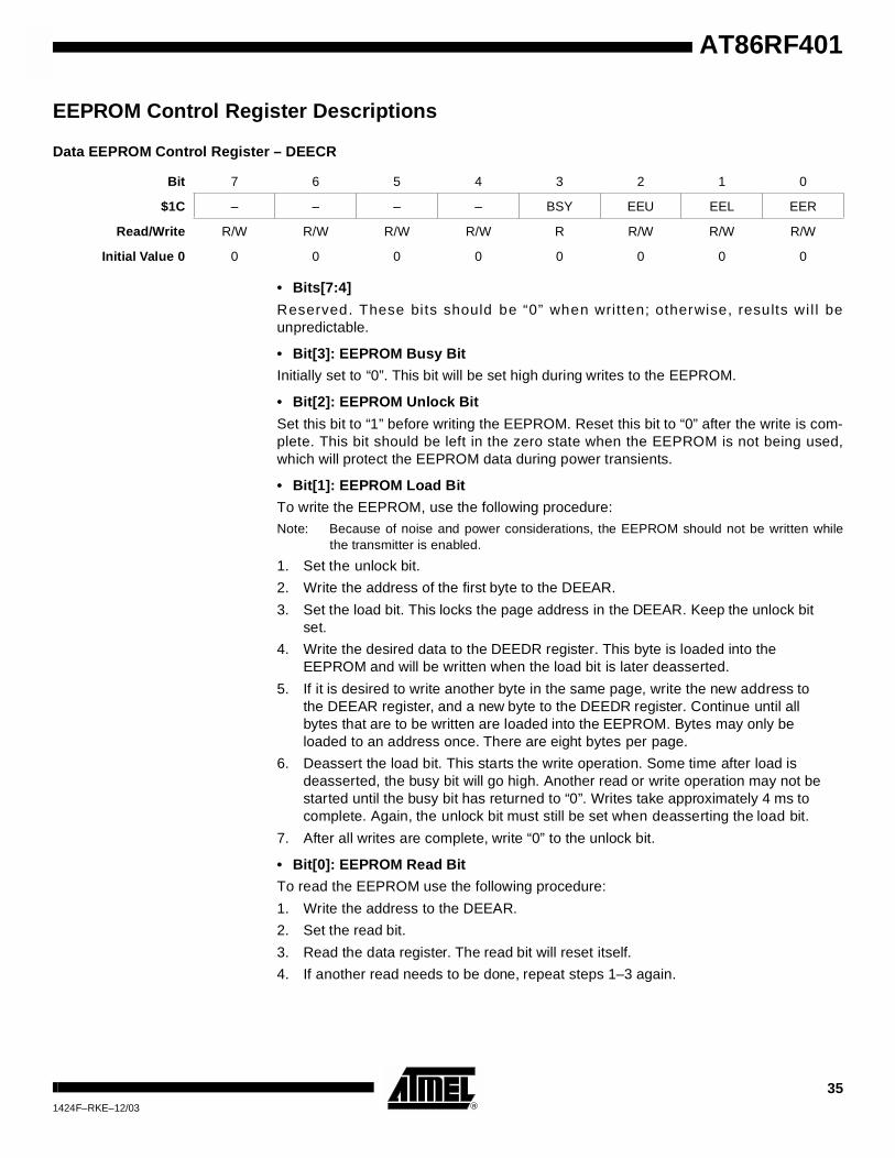
Data EEPROM Control Register – DEECR
• Bits[7:4]
Reserved. These bits should be “0” when written; otherwise, results wi l l beunpredictable.
• Bit[3]: EEPROM Busy Bit
Initially set to “0”. This bit will be set high during writes to the EEPROM.
• Bit[2]: EEPROM Unlock Bit
Set this bit to “1” before writing the EEPROM. Reset this bit to “0” after the write is com-plete. This bit should be left in the zero state when the EEPROM is not being used,which will protect the EEPROM data during power transients.
• Bit[1]: EEPROM Load Bit
To write the EEPROM, use the following procedure:
Note: Because of noise and power considerations, the EEPROM should not be written whilethe transmitter is enabled.
1. Set the unlock bit.
2. Write the address of the first byte to the DEEAR.
3. Set the load bit. This locks the page address in the DEEAR. Keep the unlock bit set.
4. Write the desired data to the DEEDR register. This byte is loaded into the EEPROM and will be written when the load bit is later deasserted.
5. If it is desired to write another byte in the same page, write the new address to the DEEAR register, and a new byte to the DEEDR register. Continue until all bytes that are to be written are loaded into the EEPROM. Bytes may only be loaded to an address once. There are eight bytes per page.
6. Deassert the load bit. This starts the write operation. Some time after load is deasserted, the busy bit will go high. Another read or write operation may not be started until the busy bit has returned to “0”. Writes take approximately 4 ms to complete. Again, the unlock bit must still be set when deasserting the load bit.
7. After all writes are complete, write “0” to the unlock bit.
• Bit[0]: EEPROM Read Bit
To read the EEPROM use the following procedure:
1. Write the address to the DEEAR.
2. Set the read bit.
3. Read the data register. The read bit will reset itself.
4. If another read needs to be done, repeat steps 1–3 again.
Bit 7 6 5 4 3 2 1 0
$1C – – – – BSY EEU EEL EER
Read/Write R/W R/W R/W R/W R R/W R/W R/W
Initial Value 0 0 0 0 0 0 0 0 0
351424F–RKE–12/03
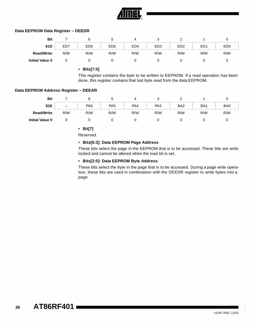
Data EEPROM Data Register – DEEDR
• Bits[7:0]
This register contains the byte to be written to EEPROM. If a read operation has beendone, this register contains that last byte read from the data EEPROM.
Data EEPROM Address Register – DEEAR
• Bit[7]
Reserved.
• Bits[6:3]: Data EEPROM Page Address
These bits select the page in the EEPROM that is to be accessed. These bits are writelocked and cannot be altered when the load bit is set.
• Bits[2:0]: Data EEPROM Byte Address
These bits select the byte in the page that is to be accessed. During a page write opera-tion, these bits are used in combination with the DEEDR register to write bytes into apage.
Bit 7 6 5 4 3 2 1 0
$1D ED7 ED6 ED5 ED4 ED3 ED2 ED1 ED0
Read/Write R/W R/W R/W R/W R/W R/W R/W R/W
Initial Value 0 0 0 0 0 0 0 0 0
Bit 7 6 5 4 3 2 1 0
$1E – PA6 PA5 PA4 PA3 BA2 BA1 BA0
Read/Write R/W R/W R/W R/W R/W R/W R/W R/W
Initial Value 0 0 0 0 0 0 0 0 0
36 AT86RF4011424F–RKE–12/03

AT86RF401
Bit Timer Register Descriptions
Bit Timer Count Register – BTCNT
• Bit [7:0]
Lowest 8 bits of countval. When combined with bits [7:6] of the BTCR register, countvaldetermines a counter value that sets the width of a mark or a space that is sent to thetransmitter. The width of the mark or space is:
PXX = PAVR * (countval +1)
where PXX is the period of the mark or space, and PAVR is the period of the AVR clockthat is determined by the ACS bits of the AVR configuration register, AVR_CONFIG.
Bit Timer Control Register – BTCR
• Bit[7:6]
Count_val[9:8]. MSB of BTCNT counter value bits.
• Bits[5:4]
Table 16. Bit Timer Mode.
• Bit[3]: Interrupts Enabled
If this bit is set, the Flag2 and Flag0 will generate their respective interrupts when theyare set. Flag0 interrupt vector is located at 0 x 04. Flag2 interrupt vector is located at0 x 02. Typically, a JMP instruction resides at these vector locations to pass control toan interrupt handler. For Flag0 only, slightly faster execution can be achieved if the JMPinstruction is eliminated, and the interrupt service routine is located beginning at 0 x 04.
Bit 7 6 5 4 3 2 1 0
$20 C7 C6 C5 C4 C3 C2 C1 C0
Read/Write R/W R/W R/W R/W R/W R/W R/W R/W
Initial Value 0 0 0 0 0 0 0 0
Bit 7 6 5 4 3 2 1 0
$21 C9 C8 M1 M0 IE F2 DATA F0
Read/Write R/W R/W R/W R/W R/W R R/W R
Initial Value 0 0 0 0 0 0 0 0
Mode[1:0] Bit Timer Function
00 Bit Timer Disabled
01 Bit Timer in Generic Timer/Counter Mode
10 Bit Timer in Receive Mode
11 Bit Timer in Transmit Mode
371424F–RKE–12/03
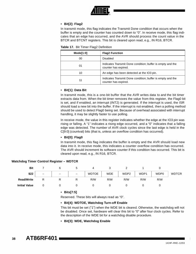
• Bit[2]: Flag2
In transmit mode, this flag indicates the Transmit Done condition that occurs when thebuffer is empty and the counter has counted down to “0”. In receive mode, this flag indi-cates that an edge has occurred, and the AVR should process the count value in theBTCR and BTCNT registers. This bit is cleared upon read, e.g., IN R16, BTCR.
Table 17. Bit Timer Flag2 Definition
• Bit[1]: Data Bit
In transmit mode, this is a one-bit buffer that the AVR writes data to and the bit timerextracts data from. When the bit timer removes the value from this register, the Flag0 bitis set, and if enabled, an interrupt (INT2) is generated. If the interrupt is used, the ISRshould load a new bit into the buffer. If the interrupt is not enabled, then a polling methodshould be used to detect Flag0 being set. Because of overhead associated with interrupthandling, it may be slightly faster to use polling.
In receive mode, the value in this register indicates whether the edge at the IO3 pin wasrising or falling. A “1” indicates a rising edge occurred, and a “0” indicates that a fallingedge was detected. The number of AVR clock cycles since the last edge is held in theC[9:0] (countval) bits (that is, unless an overflow condition has occurred).
• Bit[0]: Flag0
In transmit mode, this flag indicates the buffer is empty and the AVR should load newdata into it. In receive mode, this indicates a counter overflow condition has occurred.The AVR should increment its software counter if this condition has occurred. This bit iscleared upon read, e.g., IN R16, BTCR.
Watchdog Timer Control Register – WDTCR
• Bits[7:5]
Reserved. These bits will always read as “0”.
• Bit[4]: WDTOE, Watchdog Turn-off Enable
This bit must be set (“1”) when the WDE bit is cleared. Otherwise, the watchdog will notbe disabled. Once set, hardware will clear this bit to “0” after four clock cycles. Refer tothe description of the WDE bit for a watchdog disable procedure.
• Bit[3]: WDE, Watchdog Enable
Mode[1:0] Flag2 Function
00 Disabled
01Indicates Transmit Done condition; buffer is empty and the counter has expired.
10 An edge has been detected at the IO3 pin.
11Indicates Transmit Done condition; buffer is empty and the counter has expired.
Bit 7 6 5 4 3 2 1 0
$22 – – – WDTOE WDE WDP2 WDP1 WDP0 WDTCR
Read/Write R R R R/W R/W R/W R/W R/W
Initial Value 0 0 0 0 0 0 0 0
38 AT86RF4011424F–RKE–12/03

AT86RF401
When the WDE is set (“1”), the Watchdog Timer is enabled, and if the WDE is cleared(“0”), the Watchdog Timer function is disabled. WDE can only be cleared if the WDTOEbit is set (“1”). To disable an enabled Watchdog Timer, the following procedure must befollowed: In the same operation, write a logical “1” to WDTOE and WDE. A logical “1”must be written to WDE even though it is set to “1” before the disable operation starts.Within the next four clock cycles, write a logical “0” to WDE. This disables the watchdog.
• Bits[2:0]: WDP2, WDP1, WDP0, Watchdog Timer Prescaler 2, 1 and 0
The WDP2, WDP1 and WDP0 bits determine the Watchdog Timer prescaling when theWatchdog Timer is enabled. The different prescaling values and their correspondingtime-out periods are shown in Table 18.
Note:
Example:
If the crystal period is 50 ns and the system clock divider is set to 32 (Bits[7:5] in thePWR_CTL register are set to 010) and the WDT prescaler is set to 32K, then:
Watchdog Timeout = 50 ns × 32 × 32768 = 52 ms
I/O Enable Register – IO_ENAB
• Bit[7]
Reserved.
• Bit[6]
If set to “1”, additional hysteresis is added to the battery low and brown-out logic. SeeBL_CONFIG register description and Table 21 on page 43 for more details.
Table 18. Watchdog Timer Prescale Select
WDP2 WDP1 WDP0 Number of System Clock Cycles
0 0 0 2,048 cycles
0 0 1 4,096 cycles
0 1 0 8,192 cycles
0 1 1 16,384 cycles
1 0 0 32,768 cycles
1 0 1 65,536 cycles
1 1 0 131,072 cycles
1 1 1 262,144 cycles
Twdt XTALBperiod ACSdiv WDTdiv××=
Bit 7 6 5 4 3 2 1 0
$30 – BOHYST IOE5 IOE4 IOE3 IOE2 IOE1 IOE0
Read/Write R/W R/W R/W R/W R/W R/W R/W R/W
Initial Value 0 0 0 0 0 0 0 0
391424F–RKE–12/03
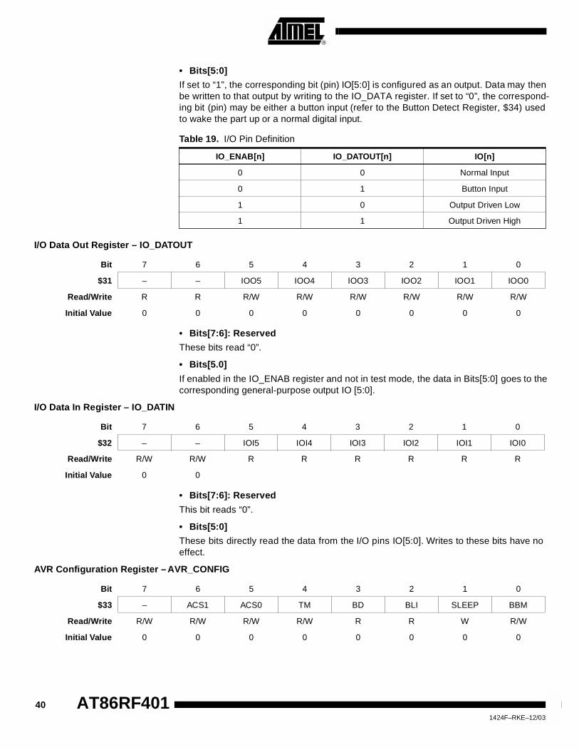
• Bits[5:0]
If set to “1”, the corresponding bit (pin) IO[5:0] is configured as an output. Data may thenbe written to that output by writing to the IO_DATA register. If set to “0”, the correspond-ing bit (pin) may be either a button input (refer to the Button Detect Register, $34) usedto wake the part up or a normal digital input.
Table 19. I/O Pin Definition
I/O Data Out Register – IO_DATOUT
• Bits[7:6]: Reserved
These bits read “0”.
• Bits[5.0]
If enabled in the IO_ENAB register and not in test mode, the data in Bits[5:0] goes to thecorresponding general-purpose output IO [5:0].
I/O Data In Register – IO_DATIN
• Bits[7:6]: Reserved
This bit reads “0”.
• Bits[5:0]
These bits directly read the data from the I/O pins IO[5:0]. Writes to these bits have noeffect.
AVR Configuration Register – AVR_CONFIG
IO_ENAB[n] IO_DATOUT[n] IO[n]
0 0 Normal Input
0 1 Button Input
1 0 Output Driven Low
1 1 Output Driven High
Bit 7 6 5 4 3 2 1 0
$31 – – IOO5 IOO4 IOO3 IOO2 IOO1 IOO0
Read/Write R R R/W R/W R/W R/W R/W R/W
Initial Value 0 0 0 0 0 0 0 0
Bit 7 6 5 4 3 2 1 0
$32 – – IOI5 IOI4 IOI3 IOI2 IOI1 IOI0
Read/Write R/W R/W R R R R R R
Initial Value 0 0
Bit 7 6 5 4 3 2 1 0
$33 – ACS1 ACS0 TM BD BLI SLEEP BBM
Read/Write R/W R/W R/W R/W R R W R/W
Initial Value 0 0 0 0 0 0 0 0
40 AT86RF4011424F–RKE–12/03

AT86RF401
• Bits[6:5]: AVR System Clock Select
These bits select the divide value of the XTALB input that is used to produce the AVRSystem Clock.
Table 20. AVR Clock Select Definition
This clock select value may be programmed on the fly by either the AVR processor innormal operation or by an I/O write SPI command during SPI mode. Note that duringSPI mode, the I/O and serial programming logic runs at XTALB/16 frequency.
• Bit[4]: Test Mode
When this bit is set to “1”, the part enters test mode. The I/O pins, if enabled, assumethe following functionality:
Notes: 1. IO_ENAB register is NOT used for SPI pins.2. In SPI mode, the I/O registers may be directly accessed via the SPI interface. Txkey, lockdetect may be output using this
mode.
• Bit[3]: Battery Dead
Indicates battery is dead. Only readable by SPI interface.
• Bit[2]: Battery Low Indicator
This bit is identical to Bit[7] of Battery Low Configuration Register ($35). When Bit[6] ofBattery Low Configuration Register ($35) is set (Battery Low Valid), a set bit in this loca-tion indicates that the battery voltage is lower than the voltage level that is determinedby Bits[5:0] of Battery Low Configuration Register ($35).
• Bit [1]: Sleep Bit
When set, this bit stops the crystal oscillator. This stops the AVR processor with the pro-gram counter frozen at the current instruction. Sleep will also stop the Watchdog Timer.The Watchdog Timer is only restarted if the part wakes up. If an I/O pin is configured asa button, a button press will start the oscillator and check the battery level. If the batterylevel is greater than the Battery Dead level, the AVR system clock is started and normalprogram execution continues. If the battery level is below the Battery Dead level, thecrystal oscillator is turned off, putting the part back to sleep until a button is pressedagain (care should be taken not to put the part to sleep unless a button is configured andenabled).
• Bit[0]: Button Boot Mode (BBM)
If the BBM bit is set and the part is brought out of sleep mode by a button input activa-tion, the part will enter the button reset state. In this state, the part will reboot and begin
ACS[1:0] AVR System Clock
11 XTALB/16
10 XTALB/32
01 XTALB/64
00 XTALB/128
I/O5 I/O4 I/O3 I/O2 I/O1 I/O0
Normal Mode(RESETB = 1)
txkey
(Output)
lockdetect
(Output)
txenable
(Output)RFU RFU RFU
SPI Mode (RESETB = 0)
txkey
(Output)
lockdetect
(Output)
txenable
(Output)SPI_CLK SDO SDI
411424F–RKE–12/03

code execution at the reset location. This bit is reset at POR and when exiting the buttonreset state. All other registers remain unchanged.
Button Detect Register – B_DET
• Bits[7:6]
Reserved. These bits read “0”.
• Bits[5:0]
When an I/O pin is configured as a button using the IO_ENAB and IO_DATOUT regis-ters and a logic low is detected on that pin, the button detect logic is activated. If the partis in sleep mode, the part responds as described in the AVR Configuration Registerdescription. If a good battery is present, the appropriate bit is set in this register. A bit inthis register is cleared by writing a “0” to it.
Battery Low Configuration Register – BL_CONFIG
• Bit[7]: Battery Low
When Bit[6] in this register is set (Battery Low Valid), the BL (Battery Low) bit indicatesthat the battery voltage is lower than the voltage level that is determined by Bit[5:0] ofthis register. It is important that the programmer also check Bit[6] (Battery Low Valid) tobe certain that this condition is valid.
• Bit[6]: Battery Low Valid
When the Battery Low Configuration Register is written, this bit is set to “0”. When thebattery voltage has been sampled and compared to the voltage determined by the BLxbits, this bit is set to “1” indicating that the data in Bit[7] (Battery Low) is valid. This cantake up to 3100 XTAL cycles to complete.
Note: The programmer should ensure that this bit is cleared prior to making a determination ofthe Battery Low status. This can be done by reloading Bit[5] or directly clearing Bit[6].Generally, the programmer loads Bit[5], loops until Bit[6] is set, and then checks Bit[3] todetermine the status of the battery.
• Bit[5:0]: Battery Low Detection Level
This value is sent to the battery monitor. The threshold is calculated using the formulasshown in Table 21 on page 43.
Note: This threshold can be set below the brown-out voltage level.
Bit 7 6 5 4 3 2 1 0
$34 – – BD5 BD4 BD3 BD2 BD1 BD0
Read/Write R R R/W R/W R/W R/W R/W R/W
Initial Value 0 0 0 0 0 0 0 0
Bit 7 6 5 4 3 2 1 0
$35 BL BLV BL5 BL4 BL3 BL2 BL1 BL0
Read/Write R R R/W R/W R/W R/W R/W R/W
Initial Value 0 0 0 0 0 0 0 0
42 AT86RF4011424F–RKE–12/03

AT86RF401
Table 21. Low Battery Detection Threshold Formulas (VREF is approximately 0.7 volts)
VDD Falling
VDD Rising
BOHYST = 1 (large hysteresis) BOHYST = 0 (small hysteresis)
VDD3.887 VREF×
10.887
63--------------- × BL[5:0]+
-----------------------------------------------------------= VDD4.05 VREF×
10.887
63--------------- × BL[5:0]+
-----------------------------------------------------------= VDD4.22 VREF×
10.887
63--------------- × BL[5:0]+
-----------------------------------------------------------=
BL[5:0] 71 3.887VREF
VDD------------- 1–××=
BL[5:0] 71 4.05VREF
VDD------------- 1–××= BL[5:0] 71 4.22
VREF
VDD------------- 1–××=
431424F–RKE–12/03

The Stack Pointer – SP The Stack Pointer is implemented as two 8-bit registers in the I/O space locations $3E($5E) and $3D ($5D). Caution: As the data memory has 224 locations, only 8 bits areused and the SPH register must be programmed to 0 x 00.
The Stack Pointer points to the data SRAM stack area where the Subroutine and Inter-rupt Stacks are located. This stack space in the data SRAM must be defined by theprogram before any subroutine calls are executed or interrupts are enabled. The StackPointer must be set to point above $60. The Stack Pointer is decremented by one whendata is pushed onto the stack with the PUSH instruction, and it is decremented by twowhen the return address is pushed onto the stack with subroutine call and interrupt. TheStack Pointer is incremented by one when data is popped from the stack with the POPinstruction, and it is incremented by two when data is popped from the stack with Returnfrom Subroutine (RET) or Return from Interrupt (RETI).
The Status Register – SREG The AVR status register – SREG – at I/O space location $3F is defined as:
• Bit[7] – I: Global Interrupt Enable
The global interrupt enable bit must be set (“1”) for the interrupts to be enabled. Theindividual interrupt enable control is then performed in the interrupt mask registers(GIMSK/TIMSK). If the global interrupt enable register is cleared (“0”), none of the inter-rupts are enabled, independent of the GIMSK/TIMSK values. The I-bit is cleared byhardware after an interrupt has occurred and is set by the RETI instruction to enablesubsequent interrupts.
• Bit[6] – T: Bit Copy Storage
The bit copy instructions BLD (Bit LoaD) and BST (Bit STore) use the T-bit as sourceand destination for the operated bit. A bit from a register in the register file can be copiedinto T by the BST instruction, and a bit in T can be copied into a bit in a register in theregister file by the BLD instruction.
• Bit[5] – H: Half Carry Flag
The half carry flag H indicates a half carry in some arithmetic operations. See Figure 10on page 21 for detailed information.
Bit 15 14 13 12 11 10 9 8
$3E – – – – – SP10 SP9 SP8 SPH
$3D SP7 SP6 SP5 SP4 SP3 SP2 SP1 SP0 SPL
7 6 5 4 3 2 1 0
Read/Write R R R R R R/W R/W R/W
R/W R/W R/W R/W R/W R/W R/W R/W
Initial Value 0 0 0 0 0 0 0 0
0 0 0 0 0 0 0 0
Bit 7 6 5 4 3 2 1 0
$3F I T H S V N Z C
Read/Write R/W R/W R/W R/W R/W R/W R/W R/W
Initial Value 0 0 0 0 0 0 0 0
44 AT86RF4011424F–RKE–12/03

AT86RF401
• Bit[4] – S: Sign Bit, S = N⊕⊕⊕⊕ V
The S-bit is always an exclusive or between the negative flag N and the two’s comple-ment overflow flag V. See Table 22 for detailed information.
• Bit[3] – V: Two’s Complement Overflow Flag
The two’s complement overflow flag V supports two’s complement arithmetics. SeeTable 22 below for detailed information.
• Bit[2] – N: Negative Flag
The negative flag N indicates a negative result after the different arithmetic and logicoperations. See Table 22 below for detailed information.
• Bit[1] – Z: Zero Flag
The zero flag Z indicates a zero result after the different arithmetic and logic operations.See Table 22 below for detailed information.
• Bit[0] – C: Carry Flag
The carry flag C indicates a carry in an arithmetic or logic operation. See Table 22 fordetailed information.
Table 22. Instruction Set
Mnemonics Operands Description Operation Flags #Clocks
Arithmetic and Logic Instructions
ADD Rd, Rr Add Two Registers Rd ← Rd + Rr Z,C,N,V,H
ADC Rd, Rr Add with Carry Two Registers Rd ← Rd + Rr + C Z,C,N,V,H 1
ADIW Rdl,K Add Immediate to Word Rdh:Rdl ← Rdh:Rdl + K Z,C,N,V,S 1
SUB Rd, Rr Subtract Two Registers Rd ← Rd - Rr Z,C,N,V,H 2
SUBI Rd, K Subtract Constant from Register Rd ← Rd - K Z,C,N,V,H 1
SBC Rd, Rr Subtract with Carry Two Registers Rd ← Rd - Rr - C Z,C,N,V,H 1
SBCI Rd, K Subtract with Carry Constant from Register
Rd ← Rd - K - C Z,C,N,V,H 1
SBIW Rdl,K Subtract Immediate from Word Rdh:Rdl ← Rdh:Rdl - K Z,C,N,V,S 1
AND Rd, Rr Logical AND Registers Rd ← Rd • Rr Z,N,V 2
ANDI Rd, K Logical AND Register and Constant
Rd ← Rd • K Z,N,V 1
OR Rd, Rr Logical OR Registers Rd ← Rd v Rr Z,N,V 1
ORI Rd, K Logical OR Register and Constant Rd ← Rd v K Z,N,V 1
EOR Rd, Rr Exclusive OR Registers Rd ← Rd ⊕ Rr Z,N,V 1
COM Rd One’s Complement Rd ← $FF − Rd Z,C,N,V 1
NEG Rd Two’s Complement Rd ← $00 − Rd Z,C,N,V,H 1
SBR Rd,K Set Bit(s) in Register Rd ← Rd v K Z,N,V 1
CBR Rd,K Clear Bit(s) in Register Rd ← Rd • ($FF - K) Z,N,V 1
INC Rd Increment Rd ← Rd + 1 Z,N,V 1
DEC Rd Decrement Rd ← Rd − 1 Z,N,V 1
TST Rd Test for Zero or Minus Rd ← Rd • Rd Z,N,V 1
451424F–RKE–12/03
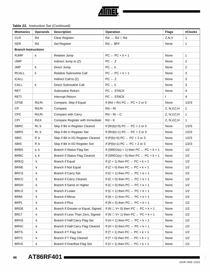
CLR Rd Clear Register Rd ← Rd ⊕ Rd Z,N,V 1
SER Rd Set Register Rd ← $FF None 1
Branch Instructions
RJMP k Relative Jump PC ← PC + k + 1 None 1
IJMP Indirect Jump to (Z) PC ← Z None 2
JMP k Direct Jump PC ← k None 2
RCALL k Relative Subroutine Call PC ← PC + k + 1 None 3
ICALL Indirect Call to (Z) PC ← Z None 3
CALL k Direct Subroutine Call PC ← k None 3
RET Subroutine Return PC ← STACK None 4
RETI Interrupt Return PC ← STACK I 4
CPSE Rd,Rr Compare, Skip if Equal if (Rd = Rr) PC ← PC + 2 or 3 None 1/2/3
CP Rd,Rr Compare Rd − Rr Z, N,V,C,H 1
CPC Rd,Rr Compare with Carry Rd − Rr − C Z, N,V,C,H 1
CPI Rd,K Compare Register with Immediate Rd − K Z, N,V,C,H 1
SBRC Rr, b Skip if Bit in Register Cleared If (Rr(b)=0) PC ← PC + 2 or 3 None 1/2/3
SBRS Rr, b Skip if Bit in Register Set If (Rr(b)=1) PC ← PC + 2 or 3 None 1/2/3
SBIC P, b Skip if Bit in I/O Register Cleared If (P(b)=0) PC ← PC + 2 or 3 None 1/2/3
SBIS P, b Skip if Bit in I/O Register Set If (P(b)=1) PC ← PC + 2 or 3 None 1/2/3
BRBS s, k Branch if Status Flag Set If (SREG(s) = 1) then PC ← PC + k + 1 None 1/2
BRBC s, k Branch if Status Flag Cleared If (SREG(s) = 0) then PC ← PC + k + 1 None 1/2
BREQ k Branch if Equal If (Z = 1) then PC ← PC + k + 1 None 1/2
BRNE k Branch if Not Equal If (Z = 0) then PC ← PC + k + 1 None 1/2
BRCS k Branch if Carry Set If (C = 1) then PC ← PC + k + 1 None 1/2
BRCC k Branch if Carry Cleared If (C = 0) then PC ← PC + k + 1 None 1/2
BRSH k Branch if Same or Higher If (C = 0) then PC ← PC + k + 1 None 1/2
BRLO k Branch if Lower If (C = 1) then PC ← PC + k + 1 None 1/2
BRMI k Branch if Minus If (N = 1) then PC ← PC + k + 1 None 1/2
BRPL k Branch if Plus If (N = 0) then PC ← PC + k + 1 None 1/2
BRGE k Branch if Greater or Equal, Signed If (N ⊕ V= 0) then PC ← PC + k + 1 None 1/2
BRLT k Branch if Less Than Zero, Signed If (N ⊕ V= 1) then PC ← PC + k + 1 None 1/2
BRHS k Branch if Half Carry Flag Set If (H = 1) then PC ← PC + k + 1 None 1/2
BRHC k Branch if Half Carry Flag Cleared If (H = 0) then PC ← PC + k + 1 None 1/2
BRTS k Branch if T Flag Set If (T = 1) then PC ← PC + k + 1 None 1/2
BRTC k Branch if T Flag Cleared If (T = 0) then PC ← PC + k + 1 None 1/2
BRVS k Branch if Overflow Flag Set If (V = 1) then PC ← PC + k + 1 None 1/2
Table 22. Instruction Set (Continued)
Mnemonics Operands Description Operation Flags #Clocks
46 AT86RF4011424F–RKE–12/03

AT86RF401
BRVC k Branch if Overflow Flag Cleared If (V = 0) then PC ← PC + k + 1 None 1/2
BRIE k Branch if Interrupt Enabled If (I = 1) then PC ← PC + k + 1 None 1/2
BRID k Branch if Interrupt Disabled If (I = 0) then PC ← PC + k + 1 None 1/2
Data Transfer Instructions
MOV Rd, Rr Move Between Registers Rd ← Rr None 1
MOVW Rd, Rr Copy Register Word Rd+1:Rd ← Rr + 1:Rr None
LDI Rd, K Load Immediate Rd ← K None 1
LD Rd, X Load Indirect Rd ← (X) None 2
LD Rd, X+ Load Indirect and Post-Inc. Rd ← (X), X ← X + 1 None 2
LD Rd, −X Load Indirect and Pre-Dec. X ← X − 1, Rd ← (X) None 2
LD Rd, Y Load Indirect Rd ← (Y) None 2
LD Rd, Y+ Load Indirect and Post-Inc. Rd ← (Y), Y ← Y + 1 None 2
LD Rd, −Y Load Indirect and Pre-Dec. Y ← Y − 1, Rd ← (Y) None 2
LDD Rd,Y+q Load Indirect with Displacement Rd ← (Y + q) None 2
LD Rd, Z Load Indirect Rd ← (Z) None 2
LD Rd, Z+ Load Indirect and Post-Inc. Rd ← (Z), Z ← Z + 1 None 2
LD Rd, −Z Load Indirect and Pre-Dec. Z ← Z − 1, Rd ← (Z) None 2
LDD Rd, Z+q Load Indirect with Displacement Rd ← (Z + q) None 2
LDS Rd, k Load Direct from SRAM Rd ← (k) None 2
ST X, Rr Store Indirect (X) ← Rr None 2
ST X+, Rr Store Indirect and Post-Inc. (X) ← Rr, X ← X + 1 None 2
ST − X, Rr Store Indirect and Pre-Dec. X ← X − 1, (X) ← Rr None 2
ST Y, Rr Store Indirect (Y) ← Rr None 2
ST Y+, Rr Store Indirect and Post-Inc. (Y) ← Rr, Y ← Y + 1 None 2
ST −Y, Rr Store Indirect and Pre-Dec. Y ← Y − 1, (Y) ← Rr None 2
STD Y+q,Rr Store Indirect with Displacement (Y + q) ← Rr None 2
ST Z, Rr Store Indirect (Z) ← Rr None 2
ST Z+, Rr Store Indirect and Post-Inc. (Z) ← Rr, Z ← Z + 1 None 2
ST −Z, Rr Store Indirect and Pre-Dec. Z ← Z − 1, (Z) ← Rr None 2
STD Z+q,Rr Store Indirect with Displacement (Z + q) ← Rr None 2
STS k, Rr Store Direct to SRAM (k) ← Rr None 2
LPM Load Program Memory R0 ← (Z) None 3
LPM Rd, Z Load Program Memory Rd ← (Z) None 3
LPM Rd, Z+ Load Program Memory and Post-Inc.
Rd ← (Z), Z ← Z+1 None 3
IN Rd, P In Port Rd ← P None 1
Table 22. Instruction Set (Continued)
Mnemonics Operands Description Operation Flags #Clocks
471424F–RKE–12/03

OUT P, Rr Out Port P ← Rr None 1
PUSH Rr Push Register on Stack STACK ← Rr None 2
POP Rd Pop Register from Stack Rd ← STACK None 2
Bit and Bit-test Instructions
SBI P, b Set Bit in I/O Register I/O(P,b) ← 1 None 2
CBI P, b Clear Bit in I/O Register I/O(P,b) ← 0 None 2
LSL Rd Logical Shift Left Rd(n+1) ← Rd(n), Rd(0) ← 0 Z,C,N,V 1
LSR Rd Logical Shift Right Rd(n) ← Rd(n+1), Rd(7) ← 0 Z,C,N,V 1
ROL Rd Rotate Left Through Carry Rd(0) ← C, Rd(n+1) ← Rd(n), C ← Rd(7) Z,C,N,V 1
ROR Rd Rotate Right Through Carry Rd(7) ← C, Rd(n) ← Rd(n+1), C ← Rd(0) Z,C,N,V 1
ASR Rd Arithmetic Shift Right Rd(n) ← Rd(n+1), n = 0...6 Z,C,N,V 1
SWAP Rd Swap Nibbles Rd(3...0) ← Rd(7...4), Rd(7...4) ← Rd(3...0) None 1
BSET s Flag Set SREG(s) ← 1 SREG(s) 1
BCLR s Flag Clear SREG(s) ← 0 SREG(s) 1
BST Rr, b Bit Store from Register to T T ← Rr(b) T 1
BLD Rd, b Bit Load from T to Register Rd(b) ← T None 1
SEC Set Carry C ← 1 C 1
CLC Clear Carry C ← 0 C 1
SEN Set Negative Flag N ← 1 N 1
CLN Clear Negative Flag N ← 0 N 1
SEZ Set Zero Flag Z ← 1 Z 1
CLZ Clear Zero Flag Z ← 0 Z 1
SEI Global Interrupt Enable I ← 1 I 1
CLI Global Interrupt Disable I ← 0 I 1
SES Set Signed Test Flag S ← 1 S 1
CLS Clear Signed Test Flag S ← 0 S 1
SEV Set Two’s Complement Overflow V ← 1 V 1
CLV Clear Two’s Complement Overflow V ← 0 V 1
SET Set T in SREG T ← 1 T 1
CLT Clear T in SREG T ← 0 T 1
SEH Set Half Carry Flag in SREG H ← 1 H 1
CLH Clear Half Carry Flag in SREG H ← 0 H 1
NOP No Operation None 1
SLEEP Sleep Not Implemented None 3
WDR Watchdog Reset (See specific description for WDR/timer) None 1
Table 22. Instruction Set (Continued)
Mnemonics Operands Description Operation Flags #Clocks
48 AT86RF4011424F–RKE–12/03

AT86RF401
Ordering Information
RF Output Ordering Code Package ApplicationTemperature
Operating Range
315 MHz AT86RF401U 20T North American −40°C to 85°C
434 MHz AT86RF401E 20T European −40°C to 85°C
264 to 456 MHz AT86RF401X 20T All Applications −40°C to 85°C
491424F–RKE–12/03

Package Drawing All devices are packaged on tape in reel; standard reel quantity is 2,500 pieces.
20A2 – TSSO
2325 Orchard ParkwaySan Jose, CA 95131
TITLE DRAWING NO.
R
REV.
6/3/02
COMMON DIMENSIONS(Unit of Measure = mm)
SYMBOL MIN NOM MAX NOTE
D 6.40 6.50 6.60 2, 5
E 6.40 BSC
E1 4.30 4.40 4.50 3, 5
A – – 1.20
A2 0.80 1.00 1.05
b 0.19 – 0.30 4
e 0.65 BSC
L 0.45 0.60 0.75
L1 1.00 REF
20A2, 20-lead (4.4 x 6.5 mm Body), 0.65 pitch, Thin Shrink Small Outline Package (TSSOP)
Notes: 1. This drawing is for general information only. Please refer to JEDEC Drawing MO-153, Variation AC, for additional information.
2. Dimension D does not include mold Flash, protrusions or gate burrs. Mold Flash, protrusions and gate burrs shall not exceed 0.15 mm (0.006 in) per side.
3. Dimension E1 does not include inter-lead Flash or protrusions. Inter-lead Flash and protrusions shall not exceed 0.25 mm (0.010 in) per side.
4. Dimension b does not include Dambar protrusion. Allowable Dambar protrusion shall be 0.08 mm total in excess of the b dimension at maximum material condition. Dambar cannot be located on the lower radius of the foot. Minimum space between protrusion and adjacent lead is 0.07 mm.
5. Dimension D and E1 to be determined at Datum Plane H.
20A2 C
L1
A
L
DA2
E E1
e
b
Top View
Side View
End View
50 AT86RF4011424F–RKE–12/03
AT86RF401
Data Sheet Change Log
Please note that the page numbers referenced below apply to this document.
Changes fromRev. 1424E-RKE-03/03 to Rev. 1424F-RKE-9/03
• Updated text in Low Battery Detection section on page 10.
• Table 3, in Low Battery Detection section on page 10 was moved to Battery Low Configuration Register section and became Table 21 (page 43).
• Updated text in Battery Low Configuration Register section (page 42).
• Renumbered tables as required to maintain proper sequence.
• Added Data Sheet Change Log section (page 51).
• Replaced “Power Control Register” with “AVR Configuration Register” in Button Detect Register section (page 42).
• Removed references to CFIL in Figures 1, 2, and 3 and Table 2.
• Changed description of Bit[2] (LOC) in Transmit Control Register section (page 30) from R/W to R and included additional descriptive text for Bit[5], Bit[4], and Bit[2].
• Added “Read Signature Byte” command to Serial Programming Instruction Set shown in Table 7 on page 15 and added Signature Bytes section on page 14.
• Added note regarding maximum output power in Power Attenuation Control Register description section (page 30).
• Added text to “Button Reset” paragraph in the Reset Sources section (page 12).
• Added text to Bit Timer section (page 11).
• Added text to Bit Timer Control Register section (page 37).
511424F–RKE–12/03
Printed on recycled paper.
Disclaimer: Atmel Corporation makes no warranty for the use of its products, other than those expressly contained in the Company’s standardwarranty which is detailed in Atmel’s Terms and Conditions located on the Company’s web site. The Company assumes no responsibility for anyerrors which may appear in this document, reserves the right to change devices or specifications detailed herein at any time without notice, anddoes not make any commitment to update the information contained herein. No licenses to patents or other intellectual property of Atmel aregranted by the Company in connection with the sale of Atmel products, expressly or by implication. Atmel’s products are not auth orized for useas critical components in life support devices or systems.
Atmel Corporation Atmel Operations
2325 Orchard ParkwaySan Jose, CA 95131, USATel: 1(408) 441-0311Fax: 1(408) 487-2600
Regional Headquarters
EuropeAtmel SarlRoute des Arsenaux 41Case Postale 80CH-1705 FribourgSwitzerlandTel: (41) 26-426-5555Fax: (41) 26-426-5500
AsiaRoom 1219Chinachem Golden Plaza77 Mody Road TsimshatsuiEast KowloonHong KongTel: (852) 2721-9778Fax: (852) 2722-1369
Japan9F, Tonetsu Shinkawa Bldg.1-24-8 ShinkawaChuo-ku, Tokyo 104-0033JapanTel: (81) 3-3523-3551Fax: (81) 3-3523-7581
Memory2325 Orchard ParkwaySan Jose, CA 95131, USATel: 1(408) 441-0311Fax: 1(408) 436-4314
Microcontrollers2325 Orchard ParkwaySan Jose, CA 95131, USATel: 1(408) 441-0311Fax: 1(408) 436-4314
La ChantrerieBP 7060244306 Nantes Cedex 3, FranceTel: (33) 2-40-18-18-18Fax: (33) 2-40-18-19-60
ASIC/ASSP/Smart CardsZone Industrielle13106 Rousset Cedex, FranceTel: (33) 4-42-53-60-00Fax: (33) 4-42-53-60-01
1150 East Cheyenne Mtn. Blvd.Colorado Springs, CO 80906, USATel: 1(719) 576-3300Fax: 1(719) 540-1759
Scottish Enterprise Technology ParkMaxwell BuildingEast Kilbride G75 0QR, Scotland Tel: (44) 1355-803-000Fax: (44) 1355-242-743
RF/AutomotiveTheresienstrasse 2Postfach 353574025 Heilbronn, GermanyTel: (49) 71-31-67-0Fax: (49) 71-31-67-2340
1150 East Cheyenne Mtn. Blvd.Colorado Springs, CO 80906, USATel: 1(719) 576-3300Fax: 1(719) 540-1759
Biometrics/Imaging/Hi-Rel MPU/High Speed Converters/RF Datacom
Avenue de RochepleineBP 12338521 Saint-Egreve Cedex, FranceTel: (33) 4-76-58-30-00Fax: (33) 4-76-58-34-80
Literature Requestswww.atmel.com/literature
1424F–RKE–12/03
© Atmel Corporation 2003. All rights reserved. Atmel® and combinations thereof are the registered trademarks of Atmel Corporation or itssubsidiaries. Other terms and product names may be the trademarks of others.