miniature 0402 surface mount technology packaged rf diodes
TRANSCRIPT
Applications• High isolation
switching
• Detection
• Mixing
• Voltage control
• Tuning
• Phase shifting
• Receiver protection
Features • Low parasitic
inductance 0.45 nH
• Low thermal impedance 50° C/W
• Small form factor 1.0 x 0.6 x 0.46 mm
• Frequency range 10 MHz–12 GHz
Miniature 0402 Surface Mount Technology Packaged RF Diodes
Skyworks offers a variety of 0402 surface mount technology (SMT) diodes including
PIN diodes for switch and attenuator applications, limiter diodes for receiver protection
applications, Schottky diodes for detector and mixer applications and tuning varactor diodes
for VCO, voltage tuned filters and phase shifter applications. These small form factor devices
offer low parasitic inductance and low thermal impedance, making them ideal for a variety
of markets including WLAN, WiMAX, cellular handset, cellular infrastructure, automotive,
CATV/Satcom, smart energy, medical, military, RFID, and test and measurement.
PIN Diodes for Switch and Attenuator Applications
Limiter Diodes for Receiver Protection Applications
Part Number Feature/Application Characteristics
SMP1345-040LF High Isolation Switching Very Low Capacitance (0.13 pF), Isolation 40 dB
SMP1340-040LF Fast Switching/High Isolation Low Capacitance, Fast Switching
SMP1321-040LF High Isolation Low Capacitance
SMP1320-040LF Moderate Power Switching Low Capacitance, Low Resistance
SMP1352-040LF High Power Switching Low Distortion
SMP1322-040LF High Isolation Switching Low Resistance (0.5 W Typ.)
SMP1302-040LF Attenuator Low Distortion, Low Drive Current
Part Number Feature/Application Characteristics
SMP1330-040LF Low Capacitance, Low Threshold Level Fast Recovery Time (5 ns Typ.)
Skyworks Green™ products are compliant to all applicable materials legislation and are halogen-free. For additional information, refer to Skyworks Definition of Green™, document number SQ04-0074.
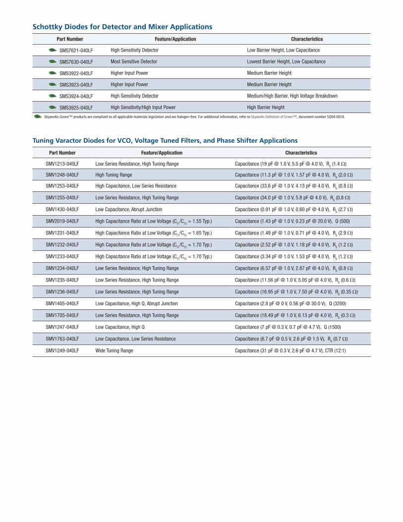
Schottky Diodes for Detector and Mixer Applications
Part Number Feature/Application Characteristics
SMS7621-040LF High Sensitivity Detector Low Barrier Height, Low Capacitance
SMS7630-040LF Most Sensitive Detector Lowest Barrier Height, Low Capacitance
SMS3922-040LF Higher Input Power Medium Barrier Height
SMS3923-040LF Higher Input Power Medium Barrier Height
SMS3924-040LF High Sensitivity Detector Medium/High Barrier, High Voltage Breakdown
SMS3925-040LF High Sensitivity/High Input Power High Barrier Height
Skyworks Green™ products are compliant to all applicable materials legislation and are halogen-free. For additional information, refer to Skyworks Definition of Green™, document number SQ04-0074.
Part Number Feature/Application Characteristics
SMV1213-040LF Low Series Resistance, High Tuning Range Capacitance (19 pF @ 1.0 V, 5.5 pF @ 4.0 V), RS (1.4 Ω)
SMV1248-040LF High Tuning Range Capacitance (11.3 pF @ 1.0 V, 1.57 pF @ 4.0 V), RS (2.0 Ω)
SMV1253-040LF High Capacitance, Low Series Resistance Capacitance (33.6 pF @ 1.0 V, 4.13 pF @ 4.0 V), RS (0.8 Ω)
SMV1255-040LF Low Series Resistance, High Tuning Range Capacitance (34.0 pF @ 1.0 V, 5.8 pF @ 4.0 V), RS (0.8 Ω)
SMV1430-040LF Low Capacitance, Abrupt Junction Capacitance (0.91 pF @ 1.0 V, 0.60 pF @ 4.0 V), RS (2.7 Ω)
SMV2019-040LF High Capacitance Ratio at Low Voltage (CT1/CT3 = 1.55 Typ.) Capacitance (1.43 pF @ 1.0 V, 0.23 pF @ 20.0 V), Q (500)
SMV1231-040LF High Capacitance Ratio at Low Voltage (CT1/CT3 = 1.65 Typ.) Capacitance (1.49 pF @ 1.0 V, 0.71 pF @ 4.0 V), RS (2.9 Ω)
SMV1232-040LF High Capacitance Ratio at Low Voltage (CT1/CT3 = 1.70 Typ.) Capacitance (2.52 pF @ 1.0 V, 1.18 pF @ 4.0 V), RS (1.2 Ω)
SMV1233-040LF High Capacitance Ratio at Low Voltage (CT1/CT3 = 1.70 Typ.) Capacitance (3.34 pF @ 1.0 V, 1.53 pF @ 4.0 V), RS (1.2 Ω)
SMV1234-040LF Low Series Resistance, High Tuning Range Capacitance (6.57 pF @ 1.0 V, 2.87 pF @ 4.0 V), RS (0.8 Ω)
SMV1235-040LF Low Series Resistance, High Tuning Range Capacitance (11.56 pF @ 1.0 V, 5.05 pF @ 4.0 V), RS (0.6 Ω)
SMV1236-040LF Low Series Resistance, High Tuning Range Capacitance (16.95 pF @ 1.0 V, 7.50 pF @ 4.0 V), RS (0.35 Ω)
SMV1405-040LF Low Capacitance, High Q, Abrupt Junction Capacitance (2.8 pF @ 0 V, 0.56 pF @ 30.0 V), Q (3200)
SMV1705-040LF Low Series Resistance, High Tuning Range Capacitance (18.49 pF @ 1.0 V, 6.13 pF @ 4.0 V), RS (0.3 Ω)
SMV1247-040LF Low Capacitance, High Q Capacitance (7 pF @ 0.3 V, 0.7 pF @ 4.7 V), Q (1500)
SMV1763-040LF Low Capacitance, Low Series Resistance Capacitance (6.7 pF @ 0.5 V, 2.6 pF @ 1.5 V), RS (0.7 Ω)
SMV1249-040LF Wide Tuning Range Capacitance (31 pF @ 0.3 V, 2.6 pF @ 4.7 V), CTR (12:1)
Tuning Varactor Diodes for VCO, Voltage Tuned Filters, and Phase Shifter Applications

PIN DiodesPIN diodes are some of the most widely used diodes in
the world and range in applications from RF switching
in satellite television receiver low noise block converters
(LNB), to automotive remote garage door openers,
to land mobile radio transceivers and cable television
automatic level controls.
PIN diodes are three layer diodes, comprised of a heavily
doped anode (the “P” layer) and a heavily doped cathode
(the “N” layer) separated by a virtually undoped intrinsic
layer (the “I” layer). Under forward bias, charge carriers
from the P and the N layers are forced into the I layer,
which reduces its RF impedance. When a reverse bias
voltage is applied across the PIN diodes, all free charge
carriers are removed from the I layer, thereby causing its
RF impedance to increase. This variable RF impedance
versus DC, or low frequency bias signal, allows the diode
to be used in RF switching circuits in which the PIN
diode is either heavily forward-biased or reverse biased.
In RF attenuation circuits, the PIN diode is utilized as a
continuously-variable RF resistance by controlling the
magnitude of the DC bias current through the diode.
Wide Bandwidth Single Pole Double Throw Switch
High Isolation PIN Diode Single Pole Double Throw Switch
RFCommonICTRL1 I CTRL2
C1C2
C3
L1
L2
L3
D1 D2
J1 J2
RFCommon Bias 2Bias 1
RF #2RF #1
RFChoke
RFChoke
CBLOCK
C BLOCKCBLOCK
SMP1321-040LF
C FILTERCFILTER
SMP1321-040LF
SMP1345-040LF
SMP1345-040 LF
RFChoke
Switching Applications
The circuit below shows a pair of PIN diodes used to
form a single pole, double throw switch. In this switch, a
positive control current typically of the order of 10 mA is
applied to one of the bias inputs to place that side of the
switch into its low insertion loss state, while a negative
bias voltage is applied to the other bias input, forcing
the diode on that side of the switch into its maximum RF
impedance state to produce high isolation on that side of
the switch.
Many other switching circuit variations exist. Please refer
to “Design with PIN Diodes” available on our Web site at
www.skyworksinc.com for more information.
Typical SPDT Switch
RFCommonICTRL1 ICTRL2
C1
C2
C3
L1
L2
L3
D1
SMP1345-040LF SMP1345-040LF
D2J1 J2
Attenuation Applications
A resistive attenuator can be built utilizing one or more
PIN diodes. In this type of circuit, the RF resistance of the
PIN diode is adjusted to a desired value by varying the
magnitude of the DC bias current applied to the diode.
This resistance produces attenuation.
The diagrams below show an attenuator that utilizes
three PIN diodes. Many other PIN diode circuit
configurations are also possible. Please refer to “Design
with PIN Diodes” available on our Web site at
www.skyworksinc.com for more information.
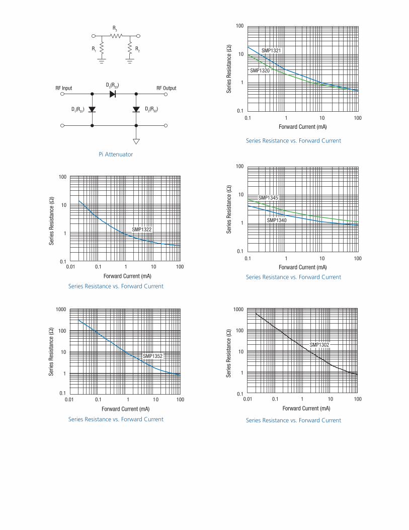
Pi Attenuator
R1
D1(RS1)
D3(RS3)
D2(RS2)
R2
RF OutputRF Input
R3
Series Resistance vs. Forward Current
0.1
1
10
100
0.1 1 10 100
Forward Current (mA)
Serie
s Re
sist
ance
(W)
SMP1320
SMP1321
Series Resistance vs. Forward Current
Series Resistance vs. Forward CurrentSeries Resistance vs. Forward Current
Series Resistance vs. Forward Current
0.1
1
10
100
0.1 1 10 100
Forward Current (mA)
Serie
s Re
sist
ance
(W)
SMP1340
SMP1345
0.01 0.1 1 10 100
Forward Current (mA)
Serie
s Re
sist
ance
(Ω)
0.1
1
10
100
1000
SMP1302
Serie
s Re
sist
ance
(W)
0.1
1
10
100
1000
0.01 0.1 1 10 100
Forward Current (mA)
SMP1352
0.10.01 0.1 1 10 100
1
10
100
Forward Current (mA)
Serie
s Re
sist
ance
(W)
SMP1322

Part Number Product Description Key Features
SMP1345-040LF High Isolation Switching PIN Diode Very Low Capacitance 0.14 pF, Isolation 40 dB
SMP1340-040LF Fast Switching/High Isolation PIN Diode Low Capacitance, Low Series Resistance
SMP1321-040LF High Isolation (LNB/Multiswitch) PIN Diode Low Capacitance, Series Pair
SMP1320-040LF Moderate Power Handling Low Capacitance, Low Resistance
SMP1352-040LF High Power Switching Lower Distortion
SMP1322-040LF High Isolation Switching Low Resistance (0.5 W Typ.)
SMP1302-040LF Attenuator Low Distortion/Low Drive Current
Part Number
Max. VR IR = 10 µA
(V)
CT VR = 30 V
(pF)
CT VR = 5 V
(pF)
CT VR = 20 V
(pF)
Typ. VF
IF = 10 mA (V)
RS IF = 1 mA
F = 100 MHz (W)
Max. RS IF = 10 mA
F = 100 MHz (W)
RS IF = 100 mA F = 100 MHz
(W)
Typ. Carrier Lifetime
IF = 10 mA (ns)
SMP1345-040LF 50 – 0.20 Max. – 0.89 3.5 Typ. 2.0 – 100
SMP1340-040LF 50 – 0.30 Max. – 0.85 – 1.2 – 100
SMP1321-040LF 100 0.025 Max. – – 0.85 3.0 Typ. 2.0 – 400
SMP1320-040LF 50 0.25 Max. – – 0.85 2.0 Typ. 0.9 – 400
SMP1352-040LF 200 – – 0.30 Max. 0.80 15 Max. 2.8 1.35 Max. 1000
SMP1322-040LF 50 1.0 Max. – – 0.85 1.5 Max. 0.5 Typ, – 400
SMP1302-040LF 200 0.30 Max. – – 0.80 20 Max. 3.0 1.5 Max. 700
PIN Diodes for Switch and Attenuator Applications
Electrical Specifications
Skyworks Green™ products are compliant to all applicable materials legislation and are halogen-free. For additional information, refer to Skyworks Definition of Green™, document number SQ04-0074.

Part NumberVB IR = 10 µA
(V)I Region Thickness
(µm) NominalCT (pF) 0 V, F = 1 MHz
CT (pF) 0 V, F = 1 GHz
RS IF = 10 mA F = 100 MHz (W)
Carrier Lifetime TL (ns) IF = 10 mA
SMP1330-040LF 20–50 2 0.7 Typ., 1.0 Max. 0.7 Typ. 1.25 Typ., 1.9 Max. 4.0 Typ.
Limiter DiodesThe PIN limiter diode can be described as an incident
power controlled, variable resistor. In the case when no
large input signal is present, the impedance of the limiter
diode is at its maximum, thereby producing minimum
insertion loss, typically less than 0.5 dB. The presence of a
large input signal temporarily forces the impedance of the
diode to a much lower value, producing an impedance
mismatch which reflects the majority of the input signal
power back towards its source.
A Single Stage Limiter
Output Power vs. Input Power for a Single Stage Limiter
SMP1330-040LFRF
Choke
DCBlock
DCBlock
Input Output
1 dB
-10-10 0 10 20 30
0
10
Outp
ut P
ower
(dBm
)
Input Power (dBm)
20
30Limiter Output Pin-IL
Low InsertionLoss Operation
LimitingOperation
Threshold Level
Part Number Feature/Application Characteristics
SMP1330-040LF Low Capacitance, Low Threshold Level Fast Recovery Time (5 ns Typ.)
Limiter Diodes for Receiver Protection Applications
Electrical Specifications
Skyworks Green™ products are compliant to all applicable materials legislation and are halogen-free. For additional information, refer to Skyworks Definition of Green™, document number SQ04-0074.
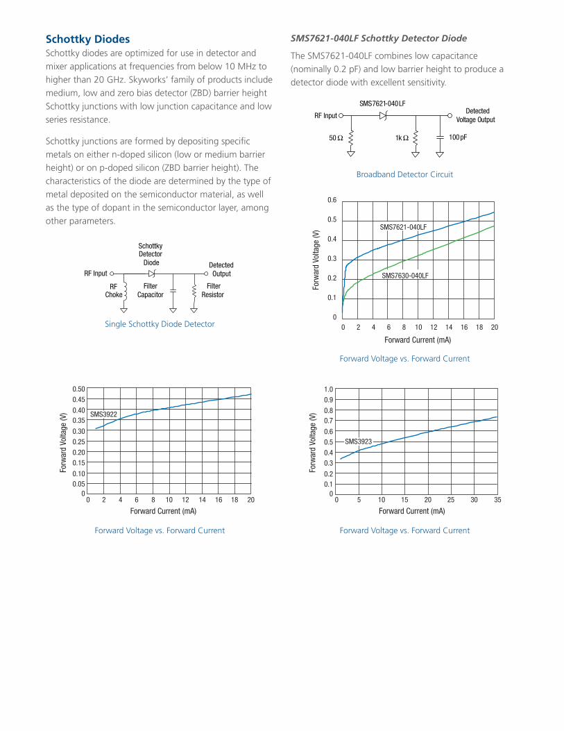
SMS7621-040LF Schottky Detector Diode
The SMS7621-040LF combines low capacitance
(nominally 0.2 pF) and low barrier height to produce a
detector diode with excellent sensitivity.
Schottky DiodesSchottky diodes are optimized for use in detector and
mixer applications at frequencies from below 10 MHz to
higher than 20 GHz. Skyworks’ family of products include
medium, low and zero bias detector (ZBD) barrier height
Schottky junctions with low junction capacitance and low
series resistance.
Schottky junctions are formed by depositing specific
metals on either n-doped silicon (low or medium barrier
height) or on p-doped silicon (ZBD barrier height). The
characteristics of the diode are determined by the type of
metal deposited on the semiconductor material, as well
as the type of dopant in the semiconductor layer, among
other parameters.
Broadband Detector Circuit
Single Schottky Diode Detector
50 Ω 1k Ω 100 pF
SMS7621-040LF
RF InputDetected
Voltage Output
Broadband Detector Circuit
RFChoke
FilterCapacitor
FilterResistor
Schottky Detector
Diode
RF InputDetected Output
0
0.1
0.2
0.3
0.4
0.5
0.6
0 2 4 6 8 10 12 14 16 18 20
Forward Current (mA)
Forw
ard
Volta
ge (V
) SMS7621-040LF
SMS7630-040LF
Forward Voltage vs. Forward Current
Forward Voltage vs. Forward CurrentForward Voltage vs. Forward Current
00.050.10
0.150.20
0.250.30
0.350.40
0.450.50
0 2 4 6 8 10 12 14 16 18 20
Forward Current (mA)
Forw
ard
Volta
ge (V
) SMS3922
00.10.2
0.30.4
0.50.6
0.70.8
0.91.0
0 5 10 15 20 25 30 35
Forward Current (mA)
Forw
ard
Volta
ge (V
)
SMS3923
Part Number
VB IR = 10 µA
(V)
Max. VF IF = 1 mA
(mV)
Max. CT VR = 0 V
(pF)
Typ. RT IF = 5 mA
F = 100 MHz (W)
Typ. RV (W)
SMS7621-040LF 2 Min. 320 0.25 18 –
SMS7630-040LF 1 Min.* 240 0.35 – 5k
SMS3922-040LF 8 Min. 340 1.03 9 –
SMS3923-040LF 20 Min. 370 1.23 10 –
SMS3924-040LF 70 Min. 550 2.25 7 @ 10 mA –
SMS3925-040LF 40 Min. 650 0.42 10 @ 10 mA –
Part Number Feature/Application Characteristics
SMS7621-040LF High Sensitivity Detector Low Barrier Height and Low Capacitance
SMS7630-040LF Most Sensitive Detector Lowest Barrier Height, Low Capacitance
SMS3922-040LF Higher Input Power Medium Barrier Height
SMS3923-040LF Higher Input Power Medium Barrier Height
SMS3924-040LF High Sensitivity/High Input Power Medium/High Barrier Height
SMS3925-040LF High Sensitivity High Barrier Height
Schottky Diodes for Detector and Mixer Applications
Electrical Specifications
*IR = 100 µA
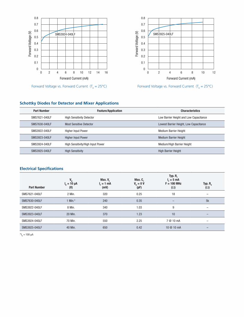
Forward Voltage vs. Forward Current (TA = 25°C)Forward Voltage vs. Forward Current (T
A = 25°C)
Forward Current (mA)
Forw
ard
Volta
ge (V
)
0
0.1
0.2
0.3
0.4
0.5
0.6
0.7
0.8
0 2 4 6 8 10 12 14 16
SMS3924-040LF
Forward Current (mA)
Forw
ard
Volta
ge (V
)
0
0.1
0.2
0.3
0.4
0.5
0.6
0.7
0.8
0 2 4 6 8 10 12
SMS3925-040LF

0
10
20
30
40
50
60
70
80
90
0 2 4 6 8 10 12 14 16 18 20
Capa
cita
nce
(pF)
Reverse Voltage (V)
SMV1249-040LFSMV1213-040LFSMV1248-040LF
SMV1253-040LFSMV1255-040LFSMV1705-040LF
Capacitance vs. Reverse Voltage
Tuning Varactor DiodesSkyworks series of silicon tuning varactor diodes are used
as the electrical tuning elements in voltage controlled
oscillators (VCOs), voltage variable analog phase shifters
and voltage tuned filters (VTFs). This family of diodes
includes abrupt junction tuning varactors, useful for low
loss, narrow band circuits, and hyperabrupt junction
varactors, useful for wide bandwidth VCOs and VTFs as
well as wide phase range variable phase shifters.
Tuning varactors are PN junction diodes. The depletion
region that forms at the junction of the diode acts as a
nearly-ideal insulator, which separates the highly-doped
anode from the cathode layer, thus forming a parallel
plate capacitor. The thickness of the depletion layer can be
increased by applying a reverse bias voltage to the diode.
The cathode layer’s doping profile is very carefully
designed to produce a tightly controlled capacitance
versus reverse bias voltage performance characteristic.
The cathode layer of an abrupt junction diode has
uniform dopant concentration throughout its thickness,
which results in a low series resistance and moderately
large change in capacitance versus bias voltage. By
contrast, the doping concentration of cathode layer of
hyperabrupt varactor diode is designed to change by
several orders of magnitude, typically over the depth of
a few microns. This non-constant dopant concentration
versus depth of the hyperabrupt diode’s cathode layer
produces a much larger available change in capacitance
versus reverse voltage, necessary for wide bandwidth or
phase shift range applications.
Typical Voltage Controlled Oscillator with a Common Cathode Pair of Tuning Varactors
RFChoke
Varactor CommonCathode Pair
L
VR
C2
VCC
RF In
RF Out
VCONTROL VCONTROL
RF Input RF Output
VCONTROL
Resonators
Phase Shifter Diagram
Voltage Tuned Filter Diagram

0
5
10
15
20
25
30
0 5 10 15 20 25 30
Capa
cita
nce
(pF)
Reverse Voltage (V)
SMV1247-040LFSMV1763-040LFSMV2019-040LFSMV1231-040LFSMV1232-040LF
SMV1233-040LFSMV1234-040LFSMV1235-040LFSMV1236-040LF
0
0.5
1.0
1.5
2.0
2.5
3.0
0 5 10 15 20 25 30
Capa
cita
nce
(pF)
Reverse Voltage (V)
SMV1430-040LF SMV1405-040LF
Capacitance vs. Reverse Voltage Capacitance vs. Reverse Voltage
Tuning Varactor Diodes for VCO, Voltage Tuned Filters, and Phase Shifter Applications
Part Number
Min. Reverse Breakdown Voltage, VR IR = 10 µA
(V)"
Typ. Total Capacitance3, CT
VR = 1 V (pF)
Typ. Total Capacitance3, CT
VR = 4 V (pF)
Typ. Total Capacitance3, CT
VR = 8 V (pF)
Min. Total Capacitance
Ratio
Capacitance Ratio Range
(V)
Max. Series
Resistance, RS (Ω)
SMV1213-040LF 12 19.13 3.87 2.4 2 1.0 to 2.5 1.4 Typ. @ 3.0 V
SMV1248-040LF 15 11.31 1.57 1.21 10.8 0.3 to 4.7 3.3 @ 3.0 V
SMV1253-040LF 15 33.69 4.63 3.4 11 0.3 to 4.7 1.4 @ 3.0 V
SMV1255-040LF 15 39.95 5.79 3.94 11 0.3 to 4.7 1.3 @ 3.0 V
SMV1430-040LF 30 0.91 0.6 0.47 3.8 0 to 30 2.7 Typ. @ 4.0 V
SMV2019-040LF 22 1.43 0.75 0.39 2.1 4 to 20 Q @ 4 V = >500
SMV1231-040LF 15 1.49 0.71 0.43 1.45 1 to 3.0 2.9 @ 3.0 V
SMV1232-040LF 15 2.52 1.18 0.71 1.5 1 to 3.0 1.5 @ 3.0 V
SMV1233-040LF 15 3.34 1.53 0.93 1.5 1 to 3.0 1.2 @ 3.0 V
SMV1234-040LF 15 6.57 2.87 1.75 1.6 1.0 to 3.0 1.2 @ 3.0 V
SMV1235-040LF 15 11.67 4.99 2.91 1.6 1.0 to 3.0 0.6 @ 3.0 V
SMV1236-040LF 15 17.02 7.19 4.49 1.6 1.0 to 3.0 0.5 @ 3.0 V
SMV1405-040LF 30 1.95 1.26 0.97 2.8 0 to 30 V 0.8 @ 4.0 V
SMV1705-040LF 12 18.49 6.13 4.08 2.8 1.0 to 4.0 0.32 Typ. @ 1.0 V
SMV1247-040LF 15 4.37 0.77 0.64 9.5 0.3 to 4.7 2.6 Typ. @ 3.0 V
SMV1763-040LF 10 5.13 1.44 1.15 2.3 0.5 to 2.5 0.7 Typ. @ 1.0 V
SMV1249-040LF 15 18.18 2.72 2.03 11.0 0.3 to 4.7 1.2 Typ. @ 3.0 V

0402 Package Information
All dimensions in millimeters
0.650
CathodeIndicator
CathodeTerminal
1.000
Bottom View
Side View
Top View
2X 0.25 ± 0.05
2X 0
.50
± 0
.05
0.46
+0.
04/–
0.06
0.05
/0.0
0
0.60
0
0.325
S1892
Package Dimensions
Part Outline
0.475
0.650
0.750
1.200
0.475
0.350
PCB Pad Metalization 2X
PCB Solder Mask Opening
All measurements in millimeters S1997
PCB Layout Footprint
S1922
A
B
2.00 ± 0.05 ∅1.55 ± 0.05 (D0)
∅0.40 ± 0.05 (D1)
CathodeIndicator
0.20
1.15
± 0
.05
(Bo)
0.70 ± 0.05 (A0)
4.00 ± 0.10
A
BB A2.00 ± 0.05
0.47 ± 0.05 (Ko)
1.75 ± 0.10
3.50
± 0
.05
8.00
± 0
.1
Notes: 1. Carrier tape: black conductive polycarbonate. 2. Cover tape: transparent conductive material. 3. Cover tape size: 5.4 mm width. 4. ESD surface resistivity is ≥1 x 10⁴ ~ ≤ 1 x 10⁸ Ohms/square. 5. All dimensions are in millimeters.
Tape and Reel Dimensions

Through our Green Initiative,™ we are committed to manufacturing products that comply with global government directives and industry requirements.
Skyworks is continuously innovating RF, analog and mixed-signal ICs. For the latest product introductions and information about Skyworks, visit our Web site at www.skyworksinc.com
For additional information on our broad overall product portfolio, please contact your local sales office or email us at [email protected].
Green Initiative™
Skyworks Solutions, Inc.20 Sylvan Road, Woburn, MA 01801USA: (781) 376-3000 • Asia: 886 2 2735 0399Europe: 33 (0)1 43548540 • Fax: (781) 376-3100Email: [email protected] • www.skyworksinc.com
BRO391-11A 9/11 Printed on Recycled Paper.