midaslcdpartnumbersystem - docs-emea.rs-online.com · character generator rom pattern 11....
TRANSCRIPT

�
�
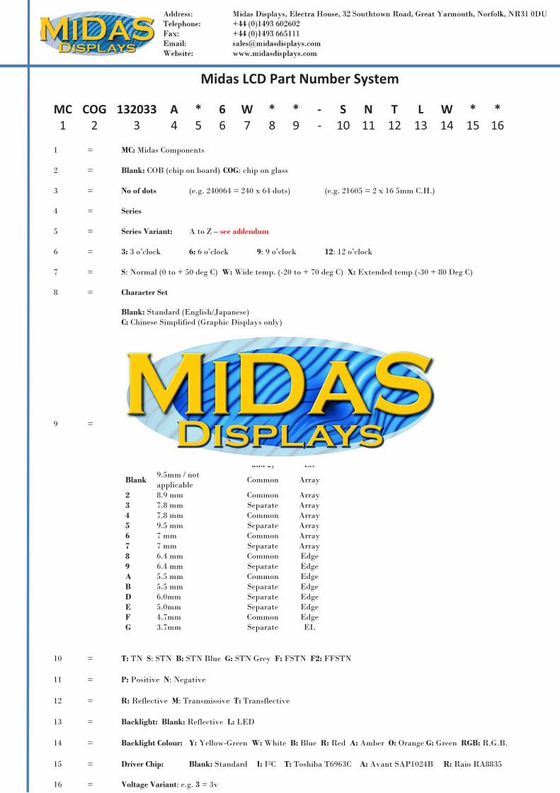
Midas�LCD�Part�Number�System��
MC� COG� 132033� A� *� 6� W * * � S N T L� W� *� * �1� 2� 3� 4� 5� 6� 7� 8 9 � 10 11 12 13� 14� 15� 16 �
1 = MC: Midas Components 2 = Blank: COB (chip on board) COG: chip on glass 3 = No of dots (e.g. 240064 = 240 x 64 dots) (e.g. 21605 = 2 x 16 5mm C.H.) 4 = Series 5 = Series Variant: A to Z – see addendum 6 = 3: 3 o’clock 6: 6 o’clock 9: 9 o’clock 12: 12 o’clock 7 = S: Normal (0 to + 50 deg C) W: Wide temp. (-20 to + 70 deg C) X: Extended temp (-30 + 80 Deg C) 8 = Character Set
Blank: Standard (English/Japanese) C: Chinese Simplified (Graphic Displays only)
CB: Chinese Big 5 (Graphic Displays only) H: Hebrew K: European (std) (English/German/French/Greek) L: English/Japanese (special) M: European (English/Scandinavian) R: Cyrillic W: European (English/Greek) U: European (English/Scandinavian/Icelandic)
9 = Bezel Height (where applicable / available)
Top of Bezel to Top
of PCB
Common (via pins 1
and 2)
Array or Edge
Lit
Blank 9.5mm / not applicable
Common Array
2 8.9 mm Common Array 3 7.8 mm Separate Array 4 7.8 mm Common Array 5 9.5 mm Separate Array 6 7 mm Common Array 7 7 mm Separate Array 8 6.4 mm Common Edge 9 6.4 mm Separate Edge A 5.5 mm Common Edge B 5.5 mm Separate Edge D 6.0mm Separate Edge E 5.0mm Separate Edge F 4.7mm Common Edge G 3.7mm Separate EL
10 = T: TN S: STN B: STN Blue G: STN Grey F: FSTN F2: FFSTN
11 = P: Positive N: Negative
12 = R: Reflective M: Transmissive T: Transflective
13 = Backlight: Blank: Reflective L: LED
14 = Backlight Colour: Y: Yellow-Green W: White B: Blue R: Red A: Amber O: Orange G: Green RGB: R.G.B.
15 = Driver Chip: Blank: Standard I: I2C T: Toshiba T6963C A: Avant SAP1024B R: Raio RA8835 16 = Voltage Variant: e.g. 3 = 3v�
Contents
1. Precautions in use of LCD Modules
2. General Specification
3. Absolute Maximum Ratings
4. Electrical Characteristics
5. Optical Characteristics
6. Interface Pin Function
7. Power Supply
8. Contour Drawing & Block Diagram
9. Function Description
10. Character Generator ROM Pattern
11. Instruction Table
12. Timing Characteristics
13. Initializing of LCM
14. Quality Assurance
15. Reliability
1. Precautions in use of LCD Modules
(1) Avoid applying excessive shocks to the module or making any alterations or modifications to it. (2) Don’t make extra holes on the printed circuit board, modify its shape or change the components
of LCD module. (3) Don’t disassemble the LCM. (4) Don’t operate it above the absolute maximum rating. (5) Don’t drop, bend or twist LCM. (6) Soldering: only to the I/O terminals. (7) Storage: please storage in anti-static electricity container and clean environment.
2. General Specification
tinU noisnemiD metI
seniL 2 x sretcarahc 8 sretcarahC fo rebmuN
Module dimensions (Without LED
Backlight) 25.0 x 17.5 x 4.3 (MAX) mm
View area 21.0 x 9.0 mm
Active area 17.6 x 6.0 mm
Dot size 0.345 x 0.345 mm
Dot pitch 0.375 x 0.375 mm
mm 595.2 x548.1 ezis retcarahC
mm 504.3 x 52.2 hctip retcarahC
evitcelfeR ,YARG ,NTS epyt DCL
61/1 ytuD
kcolc’o 6 noitcerid weiV
enon epyT thgilkcaB
3. Absolute Maximum Ratings
Item Symbol Min Max Unit
V egatloV tupnI I -0.3 VDD+0.3 V
Supply Voltage For Logic VDD-VSS -0.3 7.0 V
Supply Voltage For LCD VDD-V0 Vdd-13.5 0 V
Normal Temperature
LCM
Operating Temp. Top 0 50 °C
Storage Temp. Tstr -20 70 °C
4. Electrical Characteristics
Item Symbol Condition Min Typ Max Unit
Supply Voltage For Logic VDD-VSS 4.5 5.0 5.5 V
Supply Voltage For LCD VDD-V0 Ta=25°C 2.9 3.4 3.9 V
Input High Volt. VIH 0.7 VDD VDD V
Input Low Volt. VIL VSS 0.3 VDD V
Supply Current IDD VDD=5V 0.5 1.2 1.5 mA
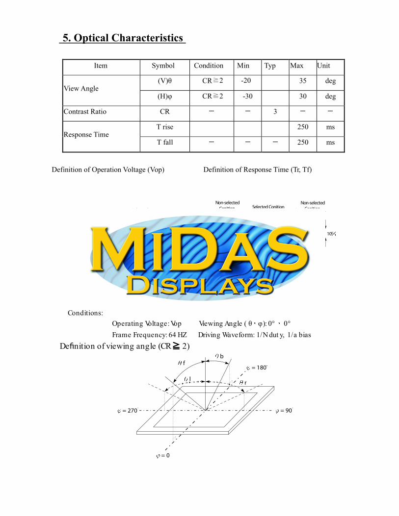
5. Optical Characteristics
Item Symbol Condition Min Typ Max Unit
View Angle (V�� CR≧ 2 -20 35 deg
(H�� CR 2 -30 30 deg
Contrast Ratio CR 3
Response Time T rise 250 ms
T fall 250 ms
Definition of Operation Voltage (Vop) Definition of Response Time (Tr, Tf)
Driving Voltage(V)
Intensity
Cr Max
100
Vop
Selected Wave
Non-selected Wave
[positive type]
Cr = Lon / Lo
Intensity
90100
Tr
10
Tf
Non-selectedConition
Non-selectedConitionSelected Conition
[positive type]
Conditions: Operating Voltage: Vop Viewing Angle ��� �): 0° 0° Frame Frequency: 64 HZ Driving Waveform: 1/N dut y, 1/a bias De nition of viewing angle (CR 2)
f= 180
= 90
= 0
= 270
b
rl

6. Interface Pin Function
Pin No. noitpircseD leveL lobmyS
1 VSS 0V Ground
2 VDD 5.0V Supply Voltage for logic
3 V0 (Variable) Operating voltage for LCD
4 RS H/L H: DATA, L: Instruction code
5 R/W H/L H: Read (MP��Module) L: Write (MP��Module)
6 E H,�L Chip enable signal
7 DB0 H/L Data bit 0
8 DB1 H/L Data bit 1
9 DB2 H/L Data bit 2
10 DB3 H/L Data bit 3
11 DB4 H/L Data bit 4
12 DB5 H/L Data bit 5
13 DB6 H/L Data bit 6
14 DB7 H/L Data bit 7
15 NC No Connection
16 NC No Connection
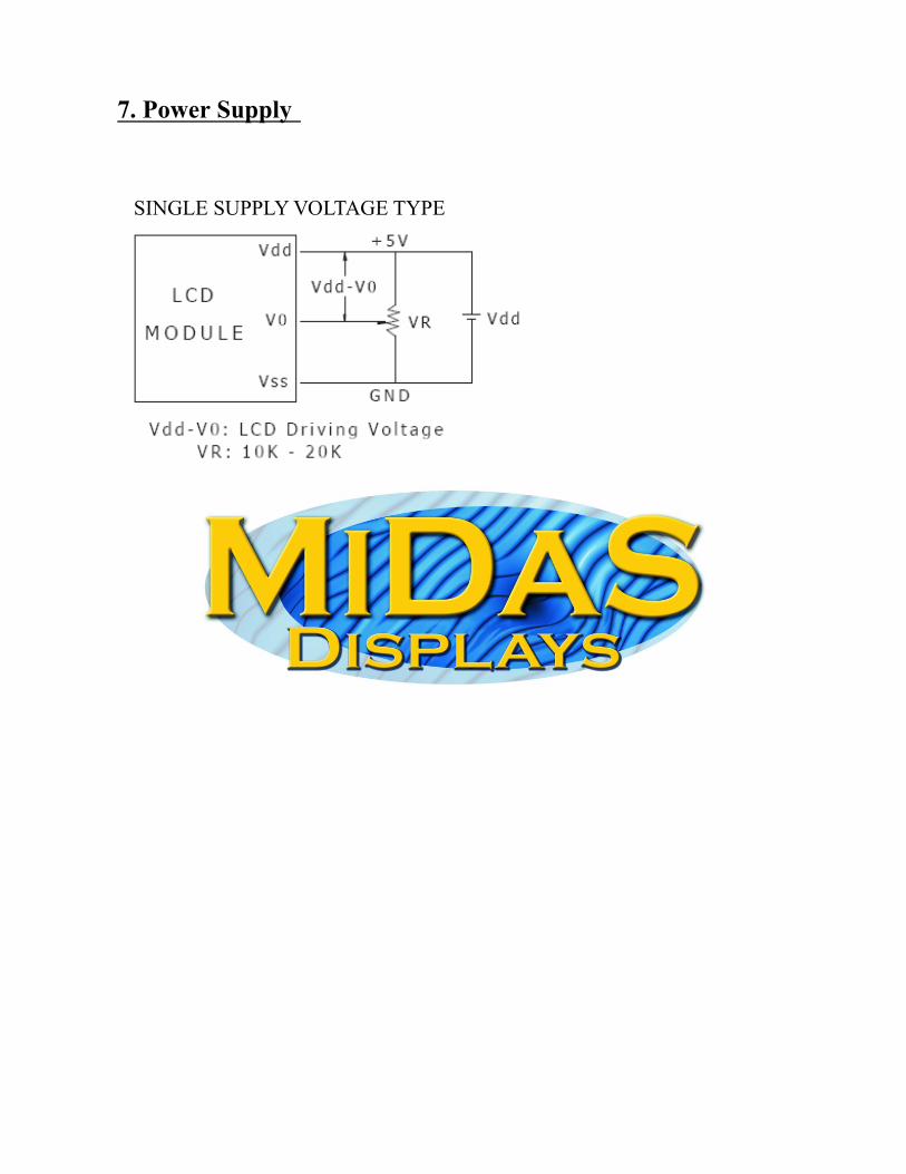
7. Power Supply
SINGLE SUPPLY VOLTAGE TYPE
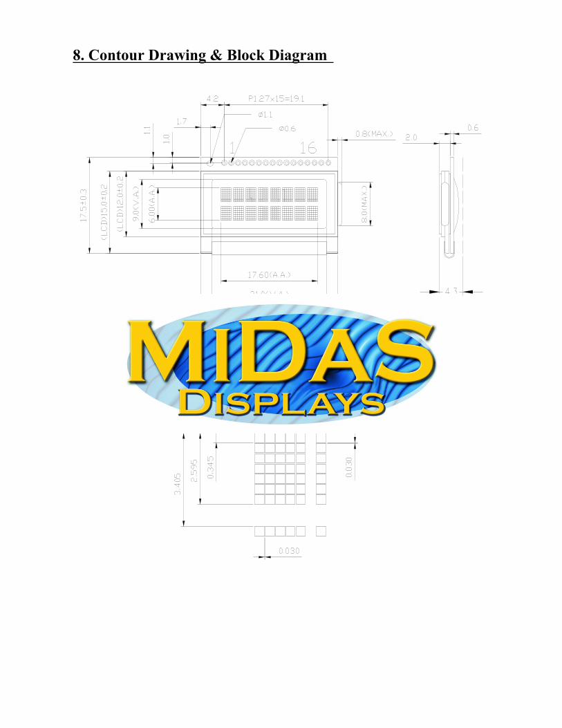
8. Contour Drawing & Block Diagram

9. Function Description
The LCD display Module is built in a LSI controller, the controller has two 8-bit registers, an instruction register (IR) and a data register (DR). The IR stores instruction codes, such as display clear and cursor shift, and address information for display data RAM (DDRAM) and character generator (CGRAM). The IR can only be written from the MPU. The DR temporarily stores data to be written or read from DDRAM or CGRAM. When address information is written into the IR, then data is stored into the DR from DDRAM or CGRAM. By the register selector (RS) signal, these two registers can be selected.
RS R/W Operation
0 0 IR write as an internal operation (display clear, etc.)
0 1 Read busy flag (DB7) and address counter (DB0 to DB7)
1 0 Write data to DDRAM or CGRAM (DR to DDRAM or CGRAM)
1 1 Read data from DDRAM or CGRAM (DDRAM or CGRAM to DR)
Busy Flag (BF)
When the busy flag is 1, the controller LSI is in the internal operation mode and the next instruction will not be accepted. When RS=0 and R/W=1, the busy flag is output to DB7. The next instruction must be written after ensuring that the busy flag is 0.
Address Counter (AC) The address counter (AC) assigns addresses to both DDRAM and CGRAM Display Data RAM (DDRAM) This DDRAM is used to store the display data represented in 8-bit character codes. Its extended capacity is 80×8 bits or 80 characters. Below figure is the relationship between DDRAM addresses and positions on the liquid crystal display.
AC (Hexadecimal)
High bits Low bits
AC6 AC5 AC4 AC3 AC2 AC1 AC0 1 0 0 1 1 1 0
Example: DDRAM addresses 4E

Character Generator ROM (CGROM) The CGROM generate 5×8 dot or 5×10 dot character patterns from 8-bit character codes. See Table 2.
Character Generator RAM (CGRAM) In CGRAM, the user can rewrite character by program. For 5×8 dots, eight character patterns
can be written, and for 5×10 dots, four character patterns can be written. Write into DDRAM the character code at the addresses shown as the left column of table 1. To show the character patterns stored in CGRAM.
Display position DDRAM address
00 01 02 03 04 05 06 07 40 41 42 43 44 45 46 47
-Line by 8-Character Display
1 2 3 4 5 6 7 8
Relationship between CGRAM Addresses, Character Cod es (DDRAM) and Character patterns
Table.1
F o r 5 * 8 d o t c h a r a c te r p a t te r n s
C h a r a c te r C o d e s( D D R A M d a ta ) C G R A M A d d r e s s C h a r a c te r P a t te r n s
( C G R A M d a ta )
5 4 3 2 1 067 5 4 3 2 01 7 6 5 4 3 2 1 0
0 0 000 110 010 101 001 111 011 100 000 110 010 101 001 111 011 100 000 1
01 001 111 011 1
* * ** * ** * ** * ** * ** * ** * ** * * 0 0 0 0 0* * ** * ** * ** * ** * ** * ** * ** * * 0 0 0 0 0
0 0 0 00 0 0 0
0 0 0 0
0 0 00 0 0
0 0 00 0 00 0 0
00 0 00 0 0
0
0 0 0
00 1
* * *
* * *
1 1 10 0 0 0 * 1 1 1
0 0 0 0 * 0 0 0
0 0 0 0 * 0 0 1
H ig h L o w H ig h L o w H ig h L o w
F o r 5 * 1 0 d o t c h a r a c te r p a t t e r n sC h a r a c te r C o d e s( D D R A M d a ta ) C G R A M A d d r e s s C h a r a c te r P a t te r n s
( C G R A M d a ta )
7
H ig h L o w
456 3 2 1 0
H ig h L o w
5 4 3 2 1 0
H ig h L o w
7 6 5 4 123 0
* * * 0 0 0 0 00 0 0 0 0* * *
* * ** * ** * ** * ** * ** * ** * ** * ** * *
* * * * * * * *
0 0 0 00 0 0 10 0 1 00 0 1 10 1 0 00 1 0 10 1 1 00 1 1 11 0 0 01 0 0 11 0 1 0
1 1 1 1
0 0 0 0 0
0 0 0 0 * 0 0 0 0 0
0 00 0
0 0 00 0 0
00 0 0 00 0 0 00 0 0 0
C h a r a c te rp a t te r n ( 1 )
C u r s o r p a t te r n
C h a r a c te rp a t te r n ( 2 )
C u r s o r p a t te r n
C h a r a c te rp a t te r n
C u r s o r p a t te r n
: " H ig h "
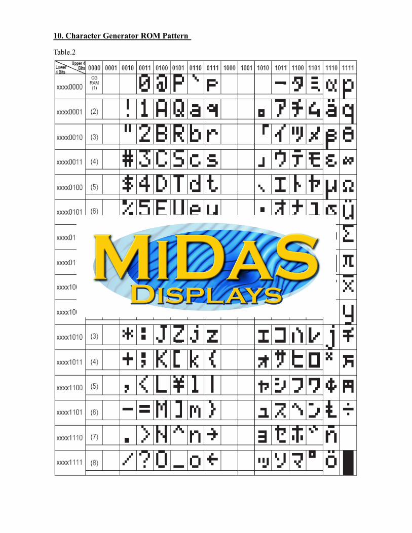
Table.2
10. Character Generator ROM Pattern

11. Instruction Table
InstructionInstruction Code
Description Execution time (fosc=270Khz)
RS R/W DB7 DB6 DB5 DB4 DB3 DB2 DB1 DB0
Clear Display 0 0 0 0 0 0 0 0 0 1 Write “00H” to DDRAM and set DDRAM address to “00H” from AC
1.53ms
Return Home 0 0 0 0 0 0 0 0 1
Set DDRAM address to “00H” from AC and return cursor to its original position if shifted. The contents of DDRAM are not changed.
1.53ms
Entry Mode Set
0 0 0 0 0 0 0 1 I/D SH Assign cursor moving direction and enable the shift of entire display.
3��
Display ON/OFF Control
0 0 0 0 0 0 1 D C B Set display (D), cursor (C), and blinking of cursor (B) on/off control bit.
3��
Cursor or Display Shift
0 0 0 0 0 1 S/C R/L Set cursor moving and display shift control bit, and the direction, without changing of DDRAM data.
3��
Function Set 0 0 0 0 1 DL N F
Set interface data length (DL:8-bit/4-bit), numbers of display line (N:2-line/1-line)and, display font type (F:5×11 dots/5×8 dots)
3��
Set CGRAM Address
0 0 0 1 AC5 AC4 AC3 AC2 AC1 AC0 Set CGRAM address in address counter. 3��
Set DDRAM Address
0 0 1 AC6 AC5 AC4 AC3 AC2 AC1 AC0 Set DDRAM address in address counter. 3��
Read Busy Flag and Address
0 1 BF AC6 AC5 AC4 AC3 AC2 AC1 AC0
Whether during internal operation or not can be known by reading BF. The contents of address counter can also be read.
��
Write Data to RAM
1 0 D7 D6 D5 D4 D3 D2 D1 D0 Write data into internal RAM (DDRAM/CGRAM).
4���
Read Data from RAM
1 1 D7 D6 D5 D4 D3 D2 D1 D0 Read data from internal RAM (DDRAM/CGRAM).
4���
” ” disregard

12. Timing Characteristics
12.1 Write Operation
Ta=25°C, VDD=5.0± 0.5V
Item Symbol Min Typ Max Unit
Enable cycle time tcycE 1200 ns
Enable pulse width (high level) PWEH 140 ns
Enable rise/fall time tEr,tEf 25 ns
Address set-up time (RS, R/W to E) tAS 0 ns
Address hold time tAH 10 ns
Data set-up time tDSW 40 ns
t emit dloh ataD H 10 ns
VIH1VIL1
VIH1VIL1
VIL1
tcycE
VIH1VIL1
VIH1VIL1
VIL1
tAS tAH
tAH
tEf
tHtDSW
PWEH
tErVIL1
VIH1VIL1
VIH1VIL1
RS
R/W
E
DB0 to DB7 Valid data

12.2 Read Operation
Ta=25°C, VDD=5.0± 0.5V
Item Symbol Min Typ Max Unit
Enable cycle time tcycE 1200 ns
Enable pulse width (high level) PWEH 140 ns
Enable rise/fall time tEr,tEf 25 ns
Address set-up time (RS, R/W to E) tAS 0 ns
Address hold time tAH 10 ns
Data delay time tDDR 100 ns
t emit dloh ataD DHR 10 ns
VIH1VIL1
VIH1VIL1
tcycE
VOH1VOL1*
tAS tAH
tAH
tEf
tDHR
PWEH
tErVIL1
VIH1VIL1
VIH1VIL1
RS
R/W
E
DB0 to DB7
VIH1 VIH1
VOH1*VOL1Valid data
tDDR
NOTE: *VOL1 is assumed to be 0.8V at 2 MHZ operation.
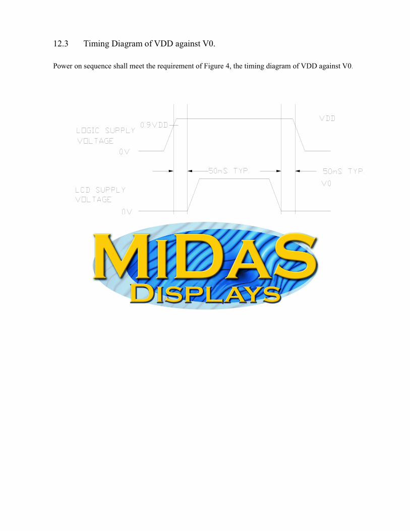
12.3 Timing Diagram of VDD against V0. Power on sequence shall meet the requirement of Figure 4, the timing diagram of VDD against V0.
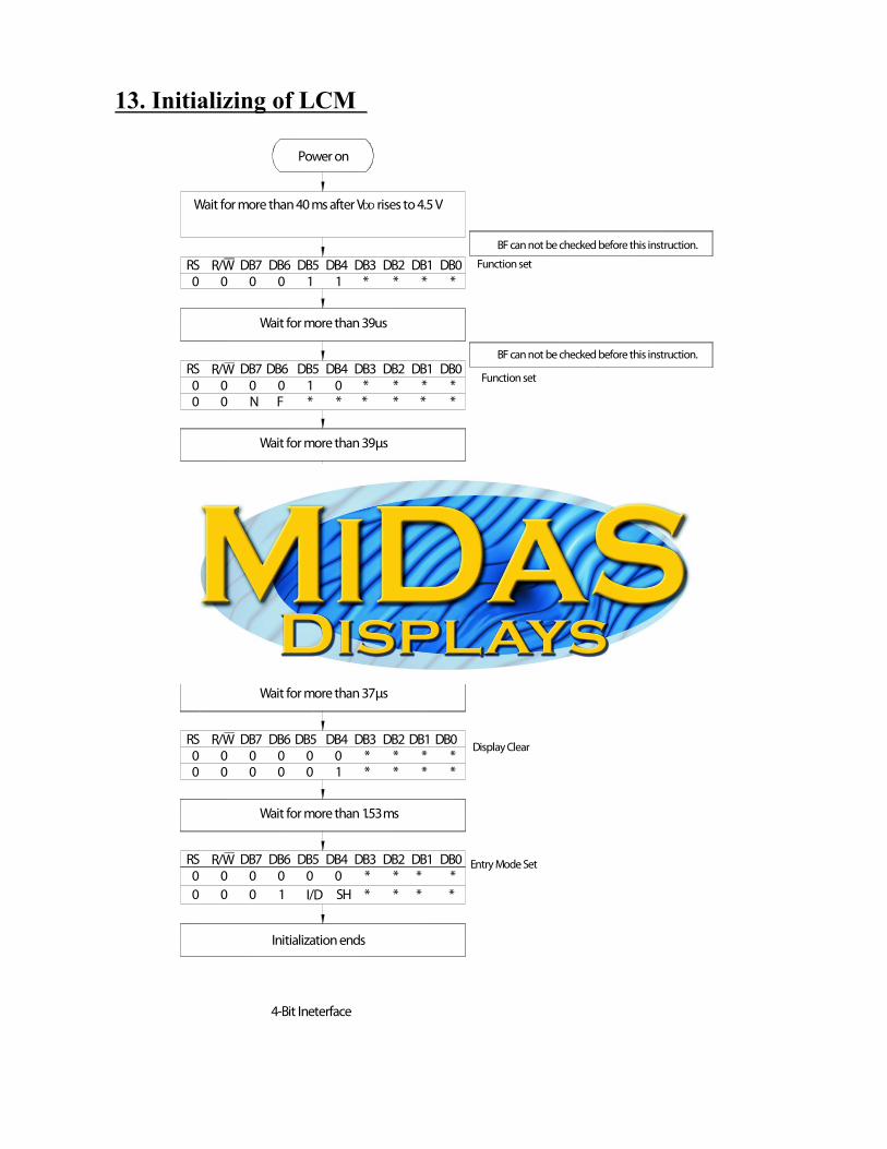
13. Initializing of LCM
0
R/W
00
R/W
00
R/W
0
0
0
0
0R/W
0R/W
Wait for more than 40 ms after VDD rises to 4.5 V
R/W
0
RS
RS0
00
RS00
0
RS0
00
RS
RS0
Display Clear
Entry Mode Set
Display ON/OFF control
4-Bit Ineterface
Initialization ends
0 1 SHI/D * ** *
Wait for more than 37 μs
DB3
Wait for more than 1.53ms
DB3
DB3
DB4DB6DB7 DB5
DB5DB70
DB60
00
00
DB400 *
010
0**
DB5DB701
0D
DB6
B0
DB40C
**
DB2 DB1 DB0*
DB0*
*
DB1DB2* *
**
**
**
DB0DB1**
DB2**
BF can not be checked before this instruction.
BF can not be checked before this instruction.
Function set
Function set
BF can not be checked before this instruction.
Wait for more than 37us
DB3
Wait for more than 39 μs
DB3
Wait for more than 39us
DB5
FN
DB70
DB60
** *0
DB41 *
DB50 0N F
DB7 DB6*1 0
** *
DB4
**
DB0
**
DB1DB2* * Function set
*
DB0***
* *
DB1DB2
DB3DB5DB70 0
DB61
DB41 *
Power on
*DB0DB1
*DB2
*
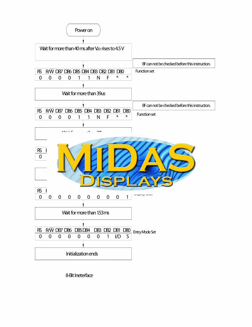
Power on
RS R/W DB7 DB6 DB5 DB4 DB3 DB2 DB1 DB0
Wait for more than 40 ms after VDD rises to 4.5 V
Wait for more than 39us
1DB4DB6
0DB5
1DB1DB2DB3
F * *DB0
DB4DB7RS R/W DB6 DB5 DB1DB2DB3 DB00 0 0 0 0 0 1 B C D
Initialization ends
BF can not be checked before this instruction.
Function set
Function set
BF can not be checked before this instruction.
8-Bit Ineterface
Wait for more than 37us
Display ON/OFF control
00 0 0 11 *F *
00 0
R/W0
R/W0
0RS
RS0
Entry Mode Set DB3
Wait for more than 1.53ms
00 000DB5DB7 DB6 DB4
I/D1 SDB0DB1DB2
Display Clear DB3
Wait for more than 37 μs
DB5DB70 0
DB6 DB400 0
DB01
DB10
DB20
RS R/W DB7
N
N

14. Quality Assurance
Screen Cosmetic Criteria noititraP noiretirC tnemgduJ tcefeD metI
1 Spots
A)Clear Size: d mm Acceptable Qty in active area
d 0.1 Disregard 0.1<d 0.2 6 0.2<d 0.3 2 0.3<d 0 Note: Including pin holes and defective dots which must
be within one pixel size. B)Unclear Size: d mm Acceptable Qty in active area d 0.2 Disregard 0.2<d 0.5 6 0.5<d 0.7 2 0.7<d 0
Minor
2 Bubbles in Polarizer
Size: d mm Acceptable Qty in active area d 0.3 Disregard 0.3<d 1.0 3 1.0<d 1.5 1 1.5<d 0
Minor
3 Scratch In accordance with spots cosmetic criteria. When the light reflects on the panel surface, the scratches are not to be remarkable.
Minor
4 Allowable Density Above defects should be separated more than 30mm each other. Minor
5 Coloration
Not to be noticeable coloration in the viewing area of the LCD panels. Back-light type should be judged with back-light on state only.
Minor

15. Reliability Content of Reliability Test
Environmental Test
noitidnoC tseT tseT fo tnetnoC metI tseT Applicable Standard
High Temperature storage
Endurance test applying the high storage temperature for a long time.
70°C 96hrs ——
Low Temperature storage
Endurance test applying the high storage temperature for a long time.
-20°C 96hrs ——
High Temperature Operation
Endurance test applying the electric stress (Voltage & Current) and the thermal stress to the element for a long time.
50°C 96hrs ——
Low Temperature Operation
Endurance test applying the electric stress under low temperature for a long time.
0°C 96hrs ——
High Temperature/ Humidity Storage
Endurance test applying the high temperature and high humidity storage for a long time.
70°C, 90%RH 96hrs ——
High Temperature/ Humidity Operation
Endurance test applying the electric stress (Voltage & Current) and temperature / humidity stress to the element for a long time.
50°C, 90%RH 96hrs ——
Temperature Cycle
Endurance test applying the low and high temperature cycle. -20°C 25°C 70°C 30min 5min 30min 1 cycle
-20°C →70°C 10 cycles ——
Mechanical Test
Vibration test Endurance test applying the vibration during transportation and using.
10~22Hz 1.5mmp-p 22~500H��1.5G Total 0.5hrs
——
Shock test Constructional and mechanical endurance test applying the shock during transportation.
50G Half sign wave 11 msedc 3 times of each direction
——
***Supply voltage for logic system=5V. Supply voltage for LCD system =Operating voltage at 25°C
�