microwave meta-material absorbers utilizing laser micro-machining
TRANSCRIPT

4
Microwave Meta-Material Absorbers Utilizing Laser
Micro-Machining Technology
Hongmin Lee Kyonggi University,
Korea
1. Introduction
Recently, artificially structured electromagnetic (EM) materials have become an extremely active research area because of the possibility of creating materials which exhibit novel EM responses not available in nature. This includes negative refractive index (NRI), super-lens, cloaking, and more generally, coordinating transformation materials. For the most part, these composites, often called meta-materials (MTMs). The double negative (DNG) MTM structure was realized in 2000 by appropriately depositing SRRs and thin-wires on dielectric substrate. Since then, most of reported designs have a 1D or 2D geometry that responds only to one (two) electrical and magnetic components of the electromagnetic fields. Much of the work in MTM has been focused on the real parts of permittivity and permeability to enable the creation of a negative refractive index material. However, they can be manipulated to create a high performance absorber. According to effective medium theory, MTMs can be represented by the complex electric permittivity ┝eff (= ┝t + j┝u) and magnetic permeability ┤eff (= ┤t + j┤u). By varying the dimensions of electric and magnetic components, it is possible to adjust permittivity and permittivity independently. Additionally, by tuning the electric and magnetic resonances a MTM can be impedance matched to free space, resulting reflectivity R = 0. The additional multiple layers or metallic back-plate will also ensure transmission T = 0. As a result, 100 % absorbance A (= 1– R – T) is theoretically possible. The microwave absorbers are used in military application to reduce the radar cross-section (RCS) of a conducting object and electromagnetic (EM) interference among microwave components. One of the earliest approaches for the design of EM absorber structure is based on the use of Salisbury screen. This type of absorber needs the resistive sheet and a metallic ground plane. The metallic backing plays two main roles; 1) it is used to avoid power transmission on the other side of the absorber, 2) it cancels out a reflected component that combined with the impinging wave. Recently, advancement in absorber technology has been obtained by using artificially MTMs to create a high-performance absorber for the microwave and terahertz frequency regime. In practice, it is difficult to make the absorber’s electrical size small enough at low frequencies. For the design of compact microwave absorbers made by MTM complimentary pairs, we need to choose proper unit cell structures which are characterized by oppositely signed values of real parts of permittivity and permittivity. However, the absorbers are usually made with metallic backing plates in order
www.intechopen.com

Micromachining Techniques for Fabrication of Micro and Nano Structures
62
to avoid power transmission on the absorbers’ other side, which may represent many problems for stealth applications. In order to design a metallic backplane-less absorber with double- negative MTM unit cell structure, we may refer to the sketch shown in Fig. 1. The two metallic pattern layers separated by dielectric spacer can be placed either orthogonal to EM wave propagation direction or parallel. If the two metallic pattern layers are placed orthogonal to EM wave propagation direction, as shown in Fig. 1(a), the radar cross section (RCS) of the object may increase at frequencies other than aimed design frequency bands.
(a) Patterns placed orthogonal to propagation direction
(b) Patterns placed parallel to propagation direction.
Fig. 1. Sketch describing the geometry of MTM absorber unit cell (where, k is the wave propagation direction).
In order to avoid this problem, the two metallic pattern layers would need to be paced parallel to EM wave propagation direction, as shown in Fig. 1(b). In this study, the proto-type absorber resonator structures were fabricated using both of a surface micromachining process technique and a standard photolithography technique.
2. Design of a miniaturized meta-material microwave absorber
2.1 Double negative unit cell design The practical implementation of a double negative MTM unit cell involves the proper choice of both the structures with the negative real part of the permittivity and the negative real part of the permeability. A single unit cell of the proposed absorber consisted of distinct metallic elements, as shown in Fig. 2(a) and 2(b). The electric responses were provided by two symmetrically placed open complimentary split ring resonators (OCSRRs), as shown in Fig 2(a). We have constructed NRI MTM unit cell using open complimentary split ring resonator (OCSRR) and split ring resonator (SRR) arrangement. The OCSRR has been derived from two former planar resonant structures: the open split ring resonator (OSRR) and the complimentary split ring resonator (CSRR). As compared to SRR and CSRR, the electrical size of OCSRR is smaller and it can be modeled as an open parallel resonant circuit. The OCSRR is modified CSRR structure exhibiting negative permittivity and the SRR structure exhibits negative permeability. Each unit cell is printed on the two side of a FR-4 substrate. We use a double-layered structure with a SRR and two OCSRRs which are put on top of each other to make a miniaturized MTM absorber unit cell for 2 GHz frequency band.
www.intechopen.com

Microwave Meta-Material Absorbers Utilizing Laser Micro-Machining Technology
63
The magnetic responses were provided by two spirals, as shown in Fig. 2(b). We created electromagnetic responses by the OCSRRs with two spirals in a parallel plane separated by a lossy dielectric substrate, as shown in Fig. 2(c). The absorber unit cell is made of a FR-4 substrate whose relative dielectric constant is ┝r = 4.4, and loss angle tangent tan ├ = 0.025, and thickness t = 0.8 mm. The metal for metallic patterns is a copper whose conductivity is σ = 5.8 ⨉ 107S/m. By changing the geometry and the separation between the OCSRRs and the spirals the electromagnetic responses are tuned to match the impedance to free space and minimize the transmission at the aimed design frequency. Computer simulations for one unit cell are carried out using the commercial finite-difference time domain solver Microwave Studio by CST. The program simulated a single unit cell with appropriate boundary conditions, as shown in Fig. 2(c). The perfect electric conductor (PEC) boundary conditions are applied to the top and bottom walls of the waveguide, where as perfect magnetic conductor (PMC) boundary conditions are applied to the side walls of the waveguide. The other two opposite sides of the waveguide is assigned as waveguide ports. The total dimension of a cell is 7.3 mm ⨉ 7 mm ⨉ 0.8 mm. A single unit cell is placed inside a waveguide, and a vertically polarized transverse electromagnetic (TEM) wave is incident normally on the front side of port 1, as shown in Fig. 2(c). The scattering parameters of this MTM unit cell were then simulated, and the absorbance was calculated using the equation A = 1- ∣S11∣2- ∣S21∣2. The simulated magnitudes of S11 and S21 parameters are plotted in Fig. 3(a). We observe that both the reflection and transmission are very low at the resonance frequency of 2.43 GHz, which indicates a strong absorption of the EM wave energy. In order to express the effective permittivity and permeability of artificial material in terms
of the scattering parameters, they are conventionally retrieved from scattering parameters of
a unit cell under plane wave excitation [11]. The impedance parameters and ABCD
parameters for two- port network can be calculated from scattering parameters using simple
transformation. Then the Bloch-Floquet theorem was used to calculate the Bloch impedance
ZB, and complex propagation constant 誌. 誌= cos-1((Z11+Z22)/2Z21)/p. (1)
Where p is the size of the MTM unit cell, and the Bloch impedance ZB can be expressed as
ZB = B/(ej誌p-A). (2)
Where, the parameter A is the voltage ratio between two ports with open-circuit at port 2
and the parameter B is the trans-admittance with short-circuit at port 2 can be expressed
using impedance parameters as
A = Z11/Z22, B = (Z11Z22 – Z212)/Z21. (3)
The effective permittivity ┝eff and permeability ┤eff can then easily calculated from Bloch
impedance and propagation constant with the free space wave number k0, and wave
impedance Z0 of the empty waveguide, respectively.
┤eff = (誌ZB)/(k0Z0). (4)
┝eff = (誌Z0)/(k0ZB). (5)
The extracted frequency dependence of the effective parameter results are plotted in Fig. 3.
The real and imaginary components ┝eff (= ┝t - j┝u) and ┤eff (= ┤t - j┤u) are plotted in Fig. 3(b)
www.intechopen.com

Micromachining Techniques for Fabrication of Micro and Nano Structures
64
and (c), respectively. There is a frequency interval, in which one effective parameter is
negative ┝t for OCSRRs, ┤t for sipral). Note that both the real components of the effective
permittivity and permeability (┝t and ┤t) are negative, and the imaginary components (┝u and
┤u) are positive at the aimed design frequency of 2.43 GHz. This meets the general condition
for the power flow and the phase velocity to be oppositely directed to the power flow,
which is written as;
┝t┤u+ ┤t┝u> 0. (6)
(a) OCSRRs (b) Spirals
(c) Single unit cell showing the direction of propagation of incident electromagnetic wave (substrate thickness t = 0.8 mm).
Fig. 2. Schematic of optimum absorber unit cell and simulation setup.
www.intechopen.com

Microwave Meta-Material Absorbers Utilizing Laser Micro-Machining Technology
65
(a) Simulated S-parameters of one unit cell (b) Effective permittivity
(c) Effective permeability (d) Refractive index
Fig. 3. Simulated results for the single absorber unit cell.
Fig. 4. Simulated absorbance of the metamaterial absorber cell.
www.intechopen.com

Micromachining Techniques for Fabrication of Micro and Nano Structures
66
(a) f = 2.43 GHz
(b) f = 2.54 GHz
Fig. 5. Simulated surface current densities in the spirals and OCSRRs.
As a result, the unit cell can be regarded as a double negative metamaterial unit cell over the
frequency range 2.43-2.45 GHz. As shown in Fig. 3(c), the imaginary part of the refractive
index is large (nu≈ 8) in the left-handed frequency region which means strong absorption of
the EM wave energy. The simulated absorbance curve over a broader frequency range is
plotted in Fig. 4. The maximum absorbance peak is 96% at 2.43 GHz, there is a secondary
absorbance peak at approximately at 2.54 Hz. In order to understand the nature of this
absorbance, the simulated surface current densities in the top resonator structure of spiral
and the lower resonator structure of OCSRRs for 2.43 and 2.54 GHz resonances are shown in
Fig. 5, respectively. For the 2.43 GHz resonance, we observe that the counter-circulating
currents flow on both the spirals provide magnetic resonance, and the stronger current
density takes place in both the shorted-end of the left-side OCSRRs, which provide electric
resonance. In contrast, the 2.54 GHz resonance is determined by the magnetic response
associated with a circulating current flowing on the right-side spiral and the electric
resonance associated with the shorted-end of the right-side OCSRR. Fig. 6 shows the
simulated S-parameters for the different horizontal spacing lengths g between the absorber
cells and the simulated results are list in the Table 1. When the spacing between two cells is
6 mm, the arrayed cell shows good impedance matched to free space impedance and
maximum absorbance.
www.intechopen.com

Microwave Meta-Material Absorbers Utilizing Laser Micro-Machining Technology
67
(a) Unit cells array (b) ∣S11∣
(c) ∣S21∣
Fig. 6. Simulated results for the different horizontal spacing lengths g between the absorber cells.
g [mm] S11 [dB] S21 [dB]
2 -11.4 -5.0
3 -12.5 -6.6
4 -13.3 -9.4
5 -13.2 -13.2
6 -13.8 -17.6
Table 1. The summary of the simulated results for the unit cells array.
www.intechopen.com

Micromachining Techniques for Fabrication of Micro and Nano Structures
68
2.2 Experimental results
(a) Absorber unit cell (b) Unit cells array in WR 430
waveguide (c) Experiment set up
Fig. 7. Photographs of the fabricated prototype absorber unit cell and unit cells array.
Fig. 8. Measured S-parameters of the planar arrayed (13 ⨉ 3) unit cells.
Fig. 9. Measured absorbance curve.
In order to verify a new type of the backplane-less absorber was designed without the resistive sheet. We fabricate a proto-type unit cell on a FR-4 substrate (┝r = 4.4, tan ├ = 0.025,
www.intechopen.com

Microwave Meta-Material Absorbers Utilizing Laser Micro-Machining Technology
69
and thickness t = 0.8 mm) using standard photolithography technique, and an experiment was carried out. The photographs of the fabricated two-layer metallization MTM absorber sample are shown in Fig. 7 (a). In order to verify the effectiveness of the double-negative MTM absorber cells without a metallic backing plate, a planar array of absorber unit cells (13 ⨉ 3) was mounted on a polystyrene foam substrate with a relative permittivity of 1.02. The inter-element spacing between two unit cells was set to 6 mm. As shown in Fig. 7 (b), this planar absorber structure was placed inside a rectangular waveguide (WR430), and measurements were taken with the waveguide over the frequency range from 1.6 GHz to 2.8 GHz. At these frequencies, the EM wave propagation was confined to the TE10 mode. The measured magnitudes of S11 and S21 parameters for the planar arrayed (13 ⨉ 3) unit cells are plotted in Fig 8. This results show that the backplane-less planar absorber structure is able to achieve the well matched broadband absorber. However, the experimental transmission minimum frequency of 2.43 GHz is shifted approximately 90 MHz lower compared to the simulated transmission minimum frequency. By using the measured S11 and S22 parameters, the calculated corresponding absorbance A (= 1- ∣S11∣2- ∣S21∣2) was plotted in Fig. 9. It exhibits a maximum absorbance of 90% at 2.34 GHz, with a full width at half maximum (FWHM) of 120 MHz over the frequency range from 2.29 to 2.41 GHz. This broader bandwidth performance is likely due to a mutual coupling effect between the cells. Although, the field distribution of the TE10 mode wave is different compared to the plane wave, the proposed planar absorber structure shows the possibility of the planar-type absorber without metallic backing plates or a resistive sheet. A new idea for a backplane-less planar-type microwave absorber based on the arrayed double-negative MTM unit cells has been presented. By properly arrayed a single unit cell with a SRR and two OCSRRs configuration, has been shown to effectively absorb most of the impinging power. The two main advantages of the proposed absorber are: 1) the absence of a metallic back plate or a resistive sheet and 2) the reduced thickness (close to 0.06┣0) in the EM wave propagation direction. The total miniaturized MTM absorber unit cell size was 7.4 mm ⨉ 7 mm ⨉ 0.8 mm. The proposed layout can be easily extended to work for more compact and thin backplane-less planar absorber designs.
3. Design of a metamaterial absorber with an enhanced operating band-width
3.1 Choice of the resonant inclusion on the edge-coupled SRRs We present the employment of the modified microwave meta-material absorber structure in order to achieve a further enhancement of the operating bandwidth. The SRRs can be used as electrically resonant particles which exhibit a strong resonant permittivity, and can also be used as the magnetic resonant particles which exhibit a strong resonant permeability. Fig. 10 shows the various types of the edge-coupled SRRs with different electromagnetic orientations. The electric field polarization is kept along the x-axis, and magnetic field polarization is kept along the y-axis. In principle, when the SRRs excited purely by magnetic field normal to the SRRs plane with electric field perpendicular to the gap (Fig. 10(b)), it exhibits a magnetic response only. SRRs excited by electric field parallel to the gap and the magnetic field lying completely in the SRRs plane (Fig. 10(d)), it exhibits an electric response only. Furthermore, the SRRs can exhibit both a purely magnetic and electric response to different electromagnetic orientation, as shown in Fig. 10(a). This results in a complicated bi-anisotropic EM behaviour. When the SRRs excited by in-plane magnetic field with electric field perpendicular to the gap (Fig. 10(c)), there is no magnetic or electric response.
www.intechopen.com

Micromachining Techniques for Fabrication of Micro and Nano Structures
70
Fig. 10. The various types of the edge-coupled SRRs with different electromagnetic orientations.
3.2 Double negative unit cell design The two type of the proposed absorber unit cells consisted of distinct metallic elements are shown in Fig. 11 (type 1) and Fig. 12 (type 2). In the absorber unit cell type 1, the purely electric and magnetic responses were provided by the two symmetrically placed OCSRRs and an SRR, respectively, as shown in Fig 11. In the absorber unit cell type 2, the purely electric responses were provided by the two OCSRRs and the electromagnetic responses were provided by the 900 rotated SRR, as shown in Fig 12.
(a) OCSRR (bottom view) (b) SRR (top view)
Fig. 11. Geometry of the absorber unit cell (type 1).
We created electromagnetic responses by combining the OCSRRs with an SRR in a parallel plane separated by a lossy dielectric substrate. The absorber unit cells are made of a FR-4 substrate whose relative dielectric constant is ┝r = 4.4, and loss angle tangent tan ├ = 0.025, and thickness t = 1.8 mm. The metal for metallic patterns is a copper whose conductivity is σ = 5.8 ⨉ 107S/m. By changing the geometry and the separation between the OCSRRs and SRR, the electromagnetic responses are tuned to match the impedance to free space and minimize the transmission at the aimed design frequency. The geometrical dimensions are: a = 7.4 mm, b = 7 mm, w = 3.2 mm, h = 6.4 mm l = 4.6 mm, and g = 0.4 mm. Computer simulations for one unit cell are carried out using the commercial finite-difference time
www.intechopen.com

Microwave Meta-Material Absorbers Utilizing Laser Micro-Machining Technology
71
(a) OCSRR (bottom view) (b) 900 rotated SRR (top view)
Fig. 12. Geometry of the absorber unit cell (type 2).
domain solver Microwave Studio by CST. The scattering parameters of theses MTM unit cells were then simulated, and the absorbance was calculated using the equation A = 1- ∣S11∣2- ∣S21∣2. The calculated absorbance is plotted in Fig. 13. In case of type 1, the maximum absorbance peak is 93% at 2.47 GHz, there is a weak secondary absorbance peak 40% at 2.98 Hz. In case of type 2, the maximum absorbance peak is 84% at 2.6 GHz, there is a strong secondary absorbance peak 86% at 2.97 Hz. When three cells are arrayed in vertical direction with a configuration of type 2, it exhibits near same absorbance characteristics. In order to understand the nature of this absorbance, the simulated surface current densities in the top resonator structure of a SRR and the lower resonator structure of OCSRRs are shown in Fig. 13 and Fig. 14, respectively.
Fig. 13. Calculated absorbance of the absorber unit cells with a different configuration.
www.intechopen.com

Micromachining Techniques for Fabrication of Micro and Nano Structures
72
(a) 2.47 GHz (b) 2.98 GHz
Fig. 14. Simulated surface current densities (type 1).
(a) 2.6 GHz (b) 2.97 GHz
Fig. 15. Simulated surface current densities (type 2).
For the 2.47 GHz resonance in type 1, we observe that the counter-circulating currents flow
on the SRR provide magnetic resonance, and the stronger current density takes place in the
shorted-end of the left-side OCSRR, which provide electric resonance. In contrast, the 2.98
GHz resonance is determined by the magnetic response associated with a circulating current
flowing on the SRR and electric resonance associated with the shorted-end of the right-side
OCSRR. For the 2.6 GHz resonance in type 2, we observe that a dipole resonance currents
and weak circulating flow on the SRR, and the stronger current density takes place in the
shorted-end of the right-side OCSRR. The 2.97 GHz resonance is determined by the
magnetic response associated with a circulating current flowing on the SRR and electric
resonance associated with the shorted-end of the left -side OCSRR.
Fig. 16 shows the sketch of the planar arrayed (13 ⨉ 4) structures of MTM absorber unit cells
of type 2. The unit cells are vertically arrayed without a gap length and the horizontally
arrayed with a spacing lengths g = 6 mm. A vertically polarized transverse electromagnetic
(TEM) wave impinges upon this structure with the incident angle from 00 to 450 and the
scattering parameters were then simulated. The simulated S-parameters are plotted in Fig.
17. We observe that the planar arrayed unit cell shows the first and secondary absorbance
peak at 2.93, and 3.27 GHz, respectively. Due to a mutual coupling effect between the cells,
the two maximum absorbance frequencies are shifted to a higher frequency band.
www.intechopen.com

Microwave Meta-Material Absorbers Utilizing Laser Micro-Machining Technology
73
Fig. 16. The planar arrayed (39 ⨉ 39) unit cells of type 2.
(a) ∣S11∣ (b) ∣S21∣ Fig. 17. The simulated S-parameters.
3.3 Experimental results In order to verify a new type of the backplane-less absorber was designed without the
resistive sheet. We fabricate a proto-type unit cell on a FR-4 substrate (┝r = 4.4, tan ├ = 0.025,
and thickness t = 1.8 mm) using standard photolithography technique, and an experiment
was carried out. The photographs of the fabricated two-layer metallization MTM absorber
sample are shown in Fig. 18 (a). In order to verify the effectiveness of the double-negative
MTM absorber cells without a metallic backing plate, a planar array of absorber unit cells
(39 ⨉ 39) was mounted on acryl test-zig, as shown in Fig. 18(b). The inter-element spacing
between two unit cells was set to 7 mm and the total size of the planar absorber was 300 m ⨉ 300 mm, and measurements were taken over the frequency range from 2.6 to 3.4 GHz. The
calculating absorbance by using the measured magnitudes of S11 and S21 parameters for the
planar arrayed absorber cells are plotted in Fig. 18 (c). With the increasing incidence angle
www.intechopen.com

Micromachining Techniques for Fabrication of Micro and Nano Structures
74
from 00 to 450 the absorbance curves have little change and the two absorbance peaks remain
more than 90% for different incident angles. For normal incident waves, the experimental data
exhibits a maximum absorbance of 93% at 2.93 GHz, with a full width at half maximum
(FWHM) of 250 MHz, and a secondary peak absorbance 87% at 3.26 GHz with a FWHM of 260
MHz. By properly arrayed a single unit cell with a 900 rotated SRR and two OCSRRs
configuration, has been shown to effectively absorb most of the impinging power. The two
main advantages of the proposed absorber are: 1) the absence of a metallic back plate or a
resistive sheet and 2) the enhanced absorbance operating band by using electromagnetic
responses of the 900 rotated SRR. The thickness of the planar MTM absorber structure in the
EM wave propagation direction was shown 7.4 mm (≈ ┣0) at 2.6 GHz. The proposed layout can
be easily extended to work for more compact and thin backplane-less planar absorber designs.
(a) One period of the arrayed unit cells.
(b) A planar arrayed MTM absorber (c) Measured absorbance
Fig. 18. Photographs of the fabricated absorber and the calculated results of the absorbance.
4. Design of a meta-material absorber applications
4.1 Three-dimensional resonator for EM waves absorption In recent years, as the use of mobile phones has become widespread, the EM waves shielding technology is a hot issue for the intelligent building construction. In this work, a three-dimensional resonators made of cubic arrangements of the OCSRRs and a metal strips is proposed. By installing these spatial band-stop cube resonators inside the concrete walls, the incident electromagnetic waves into the concrete walls can be blocked effectively over the specific frequency band. For the practical applications it is desirable to have a less sensitive to the incident angle and polarization of the impinging waves. However, it is very difficult to implement in practices due to its size and surrounding environments of the concrete. In order to solve this problem, two OCSRRs were used as basic elements and a metal strip conductor was connected between these OCSSRs. As a result, a three-dimensional resonators (7 mm ⨉ 7 mm ⨉ 7 mm) which acts individually interacting with
www.intechopen.com

Microwave Meta-Material Absorbers Utilizing Laser Micro-Machining Technology
75
(a) Geometry of one unit cell (b) Electric field distribution
(c) Surface current distribution (d) Simulated S-parameters of one unit cell
Fig. 19. Geometry of one unit cell and the simulated results.
the incoming electromagnetic waves at 2 GHz frequency band. The geometry of one unit
element and the simulated results are shown in Fig. 19. The geometrical dimensions are: a =
7 mm, b = 3.8 mm, c = 2 mm, d = 0.85 mm, and e = 0.45 mm. When the unit element is
placed within a rectangular waveguide (109 mm ⨉ 54.5 mm ⨉ 150 mm), the simulated
transmission coefficient through with/without a resonator is shown in Fig. 19 (b). The
resonance frequency of the proposed resonator shows 2.08 GHz and the stop-band width (≤
-10dB) is 19 MHz. The resonance frequency can be adjusted by the variation of the
capacitance and inductance, which depend on the physical length of the slot width, ring
spacing, ring radius, and the height of metal strip. The unit cell of the three-dimensional
resonator (7 mm ⨉ 7 mm ⨉7 mm) is shown in Fig. 20. On each side of the six sides of the
cube structures with a metallic patterns of a resonator and a lossy dielectric material (┝r =
6.0) is filled inside of the cube.
www.intechopen.com

Micromachining Techniques for Fabrication of Micro and Nano Structures
76
Fig. 20. Geometry of tree-dimensional resonator.
Fig. 21. Transmission coefficient variation for various rotated angle.
The simulated transmission coefficient variation of a resonator by the various rotated angles (θ) of a cube is shown in Fig. 21. The transmission coefficient is degenerated by the cross polarized effect and the performance of a resonator is determined by the direction of incident waves. The cubic resonator shows stop-band characteristics for a selected set of rotated angles of 0o, 45o and 90o, but its resonance frequency is changed due to anisotropic nature of the structures. The photographs of a fabricated three-dimensional resonator cubic resonator and a concrete block sample are shown in Fig. 22. The resonator structures were fabricated with a surface micromachining process on flexible polyimide substrate. A 200 ┤m-thick copper was film was e-beam evaporated on the polyimide substrate to form the ground plane. For the metallic patters, direct laser micro-machining technology was used, and another 10 ┤m-thick polyimide was coated on the top of the metallic patterns. A ‘T’-shaped metallic patterns for covering the surfaces of a cubic resonator and a photograph of the metallic-zig structure for the concrete blocks fabrication are shown in Fig. 23. In order to check the stop-band characteristics of the proposed resonator, three concrete block samples with a different cubic resonator arrangement were loaded into the jig and tested. In a measurement system, a Wiltron 360B vector network analyzer was connected to the measurement jig through an R-band waveguide to coaxial connector. A WR-430 standard waveguide, ranging from about 1.7 GHz to about 2.6 GHz, was used as a measurement jig. The WR-430 standard waveguide had a size of 10.922 cm × 5.461cm. Fig. 24 shows the
www.intechopen.com

Microwave Meta-Material Absorbers Utilizing Laser Micro-Machining Technology
77
measured transmission coefficient through the waveguide loaded with the cubic resonators array structures. We observed that the stop band-width becomes wider in comparison to the response of one cubic resonator. When nine cubic resonators are embedded into a concrete block (109 mm ⨉ 54.5 mm ⨉ 150 mm), the resonance frequency is about 2.05GHz, which is lower than simulated frequency and the stop-band width (≤ −10dB) is 150 MHz. The proposed concrete block structure can be applied to the intelligent building construction for EM waves shielding.
Fig. 22. Photographs of the fabricated three-dimensional resonator and a concrete block sample.
(a) ‘T’-shape film pattern (b) zig structure for the concrete blocks fabrication
Fig. 23. Geometry of ‘T’-shape film pattern and zig structure for fabricating the concrete blocks with cubic resonators.
(a) 3ⅹ3 cubic array (b) 3ⅹ3ⅹ2 cubic array (c) 3ⅹ5ⅹ2 cubic array
Fig. 24. Measured transmission coefficient for the different cubic resonators array.
www.intechopen.com

Micromachining Techniques for Fabrication of Micro and Nano Structures
78
4.2 Isolation improvement of two closely spaced loop antennas using double negative MTM absorber unit cells A standard method in improving isolation is to limit the radiation in the propagating
direction and to increase the distance between the antennas. However, this method is not
highly efficient because the area allocated to the antennas in mobile device is very small. In
order to improve the isolation performance several studies have been done on spatial
diversity and MIMO systems. A multiple slits etched on a single ground plane were used to
isolate the feeding port of two closely-packed antennas. Another technology is to link the
two antennas with a so-called neutralization line in order to increase the port-to-port
isolation. However, the aforementioned techniques are only suitable for mobile diversity
and MIMO antennas with a common ground plane. This study presents a new method to
improve the isolation between two antennas without a shared ground plane. In order to
increase the isolation between the two loop antennas, double negative MTM absorber unit
cells were used. The MTMs are artificial composite structures that exhibit a homogeneous
effective permittivity ┝ and permeability ┤, which become negative over an operating
frequency range. Due to the unique characteristics of the MTMs and their integration, a
number of the potential MTM applications have been researched in many small antenna
applications. A MTM absorber consists of a structure with negative permittivity and another
structure with negative permeability, resulting in a negative refractive index. We use a
double-layered structure with a SRR and two OCSRRs which are put on top of each other in
order to make a miniaturized thin MTM absorber unit cell for the 2 GHz frequency band.
Fig. 25. Geometry of the proposed loop antenna.
www.intechopen.com

Microwave Meta-Material Absorbers Utilizing Laser Micro-Machining Technology
79
The geometry of the proposed loop antenna is shown in Fig. 25. It was fed by a 50Ω coaxial
connector and designed on a FR-4 dielectric substrate (relative permittivity = 4.6, thickness =
2 mm). The proposed antenna consists of a small square loop and a SRR shaped loop. The
single loop antenna occupied 21 mm ⨉ 23.6 mm ⨉ 2 mm; the total length of the inner loop
was 54 mm long (≈ 0.5 ┣g at 2.5 GHz). The input impedance of an electrically small loop
antenna has a large inductive component. In order to match the input impedance, it needs a
capacitive element. A small capacitive split ring resonator (SRR) structure was used as a
matching element in this design. The two vertical loop arms have the same currents with a
null in middle of the top loop section. The currents are seen to be equivalent to that of a pair
of parallel monopole antennas driven in-phase with a spacing of approximately 1/8 ┣g. The
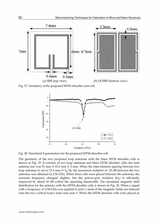
geometry of the proposed MTM absorber unit cell is shown in Fig. 27. Two OCSRRs and a
SRR structure were placed on both sides of the FR-4 dielectric substrate (relative
permittivity = 4.6, thickness = 2 mm). Two OCSRRs are located with even symmetry on one
side of the FR-4 substrate. We constructed an MTM unit cell using an OCSRR and SRR
arrangement. The proposed absorber unit cell based on the double negative MTM structure
was shown to reach a thickness on the order of 0.059 ┣0 at the frequency of 2.54 GHz. The
frequency characteristics of the unit cell structure were simulated by using a periodic
boundary condition (PBC) method; the dimensions of the unit cell were 7.4 mm × 7 mm × 2
mm. The simulated scattering parameters for the proposed unit cell are plotted in Fig. 28.
The performance of the proposed absorber shows a maximum absorbance of 93% at 2.54
GHz, and the full width at half maximum absorbance (≥ 50%) was at 200 MHz.
Fig. 26. The simulated surface current distributions.
www.intechopen.com
Micromachining Techniques for Fabrication of Micro and Nano Structures
80
(a) SRR (top view) (b) OCSRR (bottom view)
Fig. 27. Geometry of the proposed MTM absorber unit cell.
Fig. 28. Simulated S-parameters for the proposed MTM absorber cell.
The geometry of the two proposed loop antennas with the three MTM absorber cells is
shown in Fig. 29. It consists of two loop antennas and three MTM absorber cells; the total
antenna size was 51 mm ⨉ 23.6 mm ⨉ 2 mm. When the inter-element spacing between two
loop antennas is set to 13.5 mm (≈ ┣g/4), the maximum isolation of -23 dB between the two
antennas was obtained at 2.54 GHz. When three cells were placed between the antennas, the
resonant frequency changed slightly, but the port-to-port isolation ∣S21∣ is efficiently
improved by about 10 dB within the operating bandwidth. The simulated magnetic field
distribution for the antenna with the MTM absorber cells is shown in Fig. 30. When a signal
with a frequency of 2.54 GHz was applied to port 1, most of the magnetic fields are induced
onto the two vertical loop’s arms near port 1. When the MTM absorber cells were placed in
www.intechopen.com

Microwave Meta-Material Absorbers Utilizing Laser Micro-Machining Technology
81
the orthogonal direction against the magnetic fields, most of the magnetic fields were not
coupled to the loop antenna at port 2. As a result, the port-to-port isolation between the two
loop antennas was improved by using the MTM absorber cells between the two antennas. In
order to verify the simulations, two loop antennas with three double negative MTM
absorber cells were fabricated on a FR-4 substrate with the relative dielectric constant 4.6
and a thickness of 2 mm; two 50Ω SMA connecters were installed.
(a) Top view (b) Bottom view
Fig. 29. Geometry of the proposed antenna with three absorber cells.
Fig. 30. The simulated magnetic field distributions of the antenna when a signal was fed to port 1(f = 2.54GHz).
(a) Antenna with cells (b) Antenna without cells
Fig. 31. Photographs of the fabricated antenna
www.intechopen.com

Micromachining Techniques for Fabrication of Micro and Nano Structures
82
Fig. 32. Comparison of the measured return loss and isolation for the proposed antenna with/without cells.
The photographs of the prototype fabricated antennas are shown in Fig. 31. Comparisons of the measured return loss and isolation results for the proposed antennas are shown in Fig. 32. The measured S-parameters were similar to the simulated results. When three absorber cells were placed between the antennas, the isolation ∣S21∣ shows a 10 dB improvement when compared to the isolation of the antennas without the absorber cells. A maximum isolation of -24 dB was achieved at 2.54 GHz. The operating bandwidth of the proposed antenna was slightly lower due to the absorber cells between the two loop antennas. A new method to improve isolation between two closely spaced small antennas with ground plane is presented. The proposed antenna structures are composed of two small loop antennas and three double negative MTM absorber unit cells exhibiting negative permittivity and permeability at the aimed frequency of 2.54 GHz. The proposed absorber cell consists of a double-layered structure with a SRR and two OCSRRs. They are put on top of each other has shown to effectively absorb most of the impinging power. Both of them have same resonance frequency of 2.54 GHz. In order to obtain high isolation between the two closely spaced antennas, the proposed absorber cells can be effectively used. This technique can be applied for isolation improvement in multi antenna systems.
5. Conclusions
Much of the work in MTM has been focused on the real parts of the permittivity and permeability to enable the creation of a NRI material for various applications including electromagnetic wave cloaking, perfect lenses, and microwave components. By varying the dimensions of the electric and magnetic components, it is possible to adjust the permittivity and permeability independently. Additionally, by tuning the electric and magnetic resonances, an MTM can be impedance-matched to free space. As a result, 100 % absorbance is theoretically possible. By properly arrayed a single unit cell, it is possible to make the absorber’s electrical size small enough. Since from the practical point of view, it would be rather difficult to employ a photo-etching technology for the fabrication of the absorber cells, operated at the higher microwave frequency and terahertz frequency regime.
www.intechopen.com

Microwave Meta-Material Absorbers Utilizing Laser Micro-Machining Technology
83
In this work, the authors present the design and fabrication of the two-dimensional and three-dimensional microwave meta-material absorber unit cells by using a standard photolithography technique and a micro-machining technology, respectively. Moreover, a new type MTM absorber structure was proposed. By properly arrayed a single unit cell with a 900 rotated SRR and two OCSRRs configuration, has been shown to effectively absorb most of the impinging power. The two main advantages of the proposed absorber are: 1) the absence of a metallic back plate or a resistive sheet and 2) the enhanced absorbance operating band by using electromagnetic responses of the 900 rotated SRR. The thickness of the planar MTM absorber structure in the EM wave propagation direction was shown 7.4 mm (≈ ┣0) at 2.6 GHz. The proposed layout can be easily extended to work for more compact and thin backplane-less planar absorber designs.
6. Acknowledgment
This research was supported Basic Science Research Program through National Research Foundation of Korea (NRF) funded by the Ministry of Education, Science and Technology (No. 2010-0011646).”
7. References
R. L. Fnate and M. T. McCormack (1968). Reflection properties of the Salisbury screen, IEEE Trans. Antennas Propagation, vol. AP-30, no. 10, pp. 1443-1454.
N. I. Landy, S. Sajuyigbe, J. J. Mock, D. R. Smith, and W. J. Padilla (2008). Perfect metamaterial absorber, Physics Review. Lett., vol. 100, pp. 274021-4.
H. Tao, N. I. Landy, C. M. Bingham, X. Zang, R. D. Averitt, and W. J. Padilla (2008). A metamaterial absorber for the terahertz regime: design, fabrication and characterization, Optical Express, vol. 16, pp. 7181-7188.
Y. Cheng and H. Yang (2010). Design, simulation, and measurement of metamaterial absorber, Microwave Optical Technology Lett.,vol. 52, pp. 877-880.
H. Tao, C. M. Bingham, D. Pilon, K. Fan, A. C. Strkwerda, D. Shrekenhammer, W. J. Padilla, X. Zhang, and R. D. Averitt (2010). A dual band terahertz metamaterial absorber, Journal of Applied Physics D,vol. 43, pp. 225102-225106.
M. H. Li, H. L. Yang, and X. W. Hou (2010). Perfect metamaterial absorber with dual bands, Progress in Electromagnetic Research,vol. 108, pp. 37-49.
Y. Cheng, H. Yang, Z. Cheng, and N. Wu (2011). Perfect metamaterial absorber based on a split-ring-cross resonator, Journal of Applied Physics A, vol. 102, pp. 99-103.
K. B. Alici, F. Bilotti, L. Vegni, and E. Ozbay (2010). Experimental verification of metamaterial based subwavelength microwave absorbers, Applied Physics, vol.108, pp. 0831131-0831136.
A. Velez, F. Aznar, J. Bonache, J. M. Velazquez-Ahumada, and F. Martin (2009). Open complimentary split ring resonators (OCSRRs) and their application to wideband CPW band pass filters, IEEE Microwave & Wireless Component Letter, vol.19, pp. 197-199.
D. R. Smith, D. C. Vier, T. Koschny, and C. M. Soukoulis (2005). Electromgnetic parameter retrieval from inhomogeneous metamaterials, Physics Review, vol. E71, pp. 0316171-10.
www.intechopen.com

Micromachining Techniques for Fabrication of Micro and Nano Structures
84
R. A. Depine and A. Lakhtakia (2004). A new condition to identify isotropic dielectric-magnetic materials displaying negative phase velocity, Microwave Optical Technology Lett.,vol. 41, pp. 315-316.
J. Lee and S. Lim (2011). Bandwidth enhanced and polarization-insensitive metamaterial absorber using double resonance, Electron Lett., vol. 47, pp. 8-9.
M. A. Jensen J. W. Wallace (2004). A review of antennas and propagation for MIMO wireless communications, IEEE Trans. Antennas Propagation, vol. 52, pp. 2810-2824.
C. Chiu, C. Chen, D. Murch, and R. Rowell (2007). Reduction of mutual coupling between closely-packed antennas elements, IEEE Trans. Antennas Propagation, vol. 55, pp. 1732-1738.
Y. Shin and S. Park (2007). Spatial diversity antenna for WLAN application, Microwave Optical Technology Lett., vol. 49, pp. 1290-1294.
A. Diallo, C. Luxey, P. Le Thuc, and G. Kossiavas (2008). Enhanced two-antenna structures for universal mobile telecommunication system diversity terminals, Microwaves, Antennas and Propagation, IET,vol. 2, pp. 93-101.
A. Chebihi, C. Luxey, A. Diallo, P. Le Thuc, and R. Staraj (2008). A noval isolation technique for closely spaced PIFAs UMTS mobile phones, IEEE Trans. Antennas Propagation, vol. 7, pp. 665-668.
N. Engheta and R. W. Ziolkowski (2006). Metamaterials: physics and engineering explorations, Wiley-Inter-sciencce, NJ.
F. Falcone, T. Lopetegi, J. D. Baena, R. Marques, and M. Sorolla (2004). Effective negtive-┝ stop-band microstrip lines based on complementary split ring resonators, IEEE Microwave & Wireless Component Lett., vol. 14, pp. 280-282.
D. R. Smith, D. C. Vier, T. Koschny, and C. M. Soukoulis (2005). Electromgnetic parameter retrieval from inhomogeneous metamaterials, Physics Review, vol. E71, pp. 0316171-10.
www.intechopen.com

Micromachining Techniques for Fabrication of Micro and NanoStructuresEdited by Dr. Mojtaba Kahrizi
ISBN 978-953-307-906-6Hard cover, 300 pagesPublisher InTechPublished online 03, February, 2012Published in print edition February, 2012
InTech EuropeUniversity Campus STeP Ri Slavka Krautzeka 83/A 51000 Rijeka, Croatia Phone: +385 (51) 770 447 Fax: +385 (51) 686 166www.intechopen.com
InTech ChinaUnit 405, Office Block, Hotel Equatorial Shanghai No.65, Yan An Road (West), Shanghai, 200040, China
Phone: +86-21-62489820 Fax: +86-21-62489821
Micromachining is used to fabricate three-dimensional microstructures and it is the foundation of a technologycalled Micro-Electro-Mechanical-Systems (MEMS). Bulk micromachining and surface micromachining are twomajor categories (among others) in this field. This book presents advances in micromachining technology. Forthis, we have gathered review articles related to various techniques and methods of micro/nano fabrications,like focused ion beams, laser ablation, and several other specialized techniques, from esteemed researchersand scientists around the world. Each chapter gives a complete description of a specific micromachiningmethod, design, associate analytical works, experimental set-up, and the final fabricated devices, followed bymany references related to this field of research available in other literature. Due to the multidisciplinary natureof this technology, the collection of articles presented here can be used by scientists and researchers in thedisciplines of engineering, materials sciences, physics, and chemistry.
How to referenceIn order to correctly reference this scholarly work, feel free to copy and paste the following:
Hongmin Lee (2012). Microwave Meta-Material Absorbers Utilizing Laser Micro-Machining Technology,Micromachining Techniques for Fabrication of Micro and Nano Structures, Dr. Mojtaba Kahrizi (Ed.), ISBN:978-953-307-906-6, InTech, Available from: http://www.intechopen.com/books/micromachining-techniques-for-fabrication-of-micro-and-nano-structures/microwave-meta-material-absorbers-utilizing-laser-micro-machining-technology

© 2012 The Author(s). Licensee IntechOpen. This is an open access articledistributed under the terms of the Creative Commons Attribution 3.0License, which permits unrestricted use, distribution, and reproduction inany medium, provided the original work is properly cited.