microwave absorption, conductivity and - … in electromagnetics research c, vol. 8, 149{160, 2009...
TRANSCRIPT
Progress In Electromagnetics Research C, Vol. 8, 149–160, 2009
MICROWAVE ABSORPTION, CONDUCTIVITY ANDCOMPLEX PEMITTIVITY OF FRITLESS Ni(1−x)CuxMn2O4
(0 ≤ x ≤ 1) CERAMIC THICK FILM: EFFECT OF COPPER
R. N. Jadhav and V. Puri
Thick and Thin Film Device Lab, Department of PhysicsShivaji UniversityKolhapur 416004, India
Abstract—The effect of copper on the microwave absorption,conductivity and complex permittivity of fritless Ni(1−x)CuxMn2O4
(x = 0, 0.4, 0.8, 1) thick film on alumina have been investigated in the8–18GHz frequency range. The structural changes have been identifiedby scanning electron microscope (SEM), FTIR and RAMAN scatteringspectroscopy. The microwave conductivity and permittivity increase ascopper content increases. The fritless Ni(1−x)CuxMn2O4 (0 ≤ x ≤ 1)thick film with x = 0.4 shows best absorption properties, though allthe other compositions also show good absorption in a large frequencyrange. The microwave conductivity increases from 1S/cm to 951 S/cmdue to copper and the dielectric constant (ε) increases from 7 to 19.5.
1. INTRODUCTION
Due to the proliferation in the use of the electromagnetic waveespecially the radio frequency for a variety of applications the problemof electromagnetic wave pollution has attracted the attention ofresearchers. Materials which can absorb microwaves can eliminateelectromagnetic wave pollution. Wide spread applications ofelectromagnetic absorbers have inspired engineers to explore optimaldesign with available algorithms. Ideally a thin, light weight andwideband absorber is an optimum one [1]. The main mechanism ofmicrowave absorber is purely dielectric, polarization and conductivelosses [2]. Dielectric material for microwave applications shouldin general satisfy three requirements: high dielectric constant,
Corresponding author: V. Puri (vrp [email protected]).
150 Jadhav and Puri
low dielectric loss and small temperature coefficient of resonantfrequency [3]. Many techniques have been developed to measurethe permittivity [4, 5]. The complex permittivity is an importantfactor which can be altered to achieve maximum absorption of theelectromagnetic waves. Permittivity relates to the material’s ability totransmit (or permit) an electric field. Permittivity also depends on thephysical properties such as density and composition of the material,and it changes with temperature and frequency.
Thick film technology has been proved to be cost effective methodhighly conducive to planarization. Thick film thermistor is a devicethat can be used in high frequency range. This is possible due tothe development of new thick film thermistor material [6]. Nickelmanganite has an intermediate cubic structure consisting 3d transitionmetals which have negative temperature coefficient (NTC) [7]. Thecomposition of solid solution of 3d strongly affects the distribution ofcations and thus change the properties [8, 9]. Oxalate co-precipitationmethod [10] can be used to synthesize single phase, homogeneous, finegrained ceramic.
In this paper, we report the effect of copper content on themicrowave properties of fritless (glass free) Ni(1−x)CuxMn2O4 (0 ≤x ≤ 1) thick film NTC ceramic. Ni(1−x)CuxMn2O4 (0 ≤ x ≤ 1)was prepared by oxalic precursor method. Effect of copper contentin the nickel manganite thick film was also studied by structuralcharacterization using X-ray diffraction spectroscopy (XRD), Fouriertransform infrared (FTIR), RAMAN spectroscopy and Scanningelectron microscope (SEM).
2. EXPERIMENTAL PROCEDURE
The Ni(1−x)CuxMn2O4 (0 ≤ x ≤ 1) powder was prepared by oxalicprecursor method using nickel acetate, manganese acetate, copperacetate of definite proportion mixed with 2 M hot oxalic acid solutionwith constant stirring. The chemicals were weighted according torequired stoichiometry proportion by varying x = 0, 0.4, 0.8, 1. Theprepared precipitate was filtered, washed with distilled water and driedat 400◦C and finally sintered at 1000◦C for 8 Hrs.
Thick film paste was prepared by mixing in agate mortar 80 wt%of the ceramic powder, 12wt% of inorganic binder (75 wt% Bi2O3 and25%PbO) and organic vehicle (8wt%) for 2Hrs. The organic vehiclewas a solution of ethyl cellulose and [2-(2-butoxyethoxy) ethyl]-acetate.The fritless Ni(1−x)CuxMn2O4 (0 ≤ x ≤ 1) thick film was delineatedon 96% alumina by screen printing and firing at 900◦C in zonal furnacefor 1 Hr. The thickness of the Ni(1−x)CuxMn2O4 (x = 0.0, 0.4, 0.8, 1)

Progress In Electromagnetics Research C, Vol. 8, 2009 151
thick films which has rectangular shape with 1.1 cm width and 2.5 cmin height is ∼ 14µm was obtained from gravimetric method.
The formation of spinel structure was confirmed by XRD usingCu-Kα radiation, (λ = 1.541838 A0) (Philips Diffractometer PW3710), structural changes observed by FTIR (Perkin-Elmer200),RAMAN (Bruker, Multi-RAMAN spectrometer (RAM-II)), surfacemorphological studied by SEM (JSM-6360 JEOL, Japan).
Transmission of microwaves due to thick film was measuredpoint by point using transmission/reflection method with rectangularwaveguide, consisting of the X and Ku band generator, isolator,attenuator, directional coupler and RF detector. The compositiondependent permittivity was measured in microwave frequency region8.2GHz to 18 GHz (X and Ku band) by VSWR method.
3. RESULTS AND DISCUSSIONS
The typical XRD pattern of Ni(1−x)CuxMn2O4 (x = 0, 0.4, 1)thick film is shown in Fig. 1. It is observed that polycrystallineNi(1−x)CuxMn2O4 (0 ≤ x ≤ 1) was formed with dominant (311) planewhich confirmed spinel structure. All peaks appearing in XRD patternfor Ni(1−x)CuxMn2O4 (0 ≤ x ≤ 1) are very sharp indicating that thesamples have high crystallinity. The miller index for each peak wasdetermined based on a spinel structure of space group Fd3m.
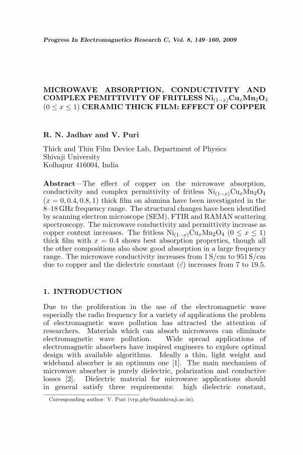
Figure 2 shows the SEM (JSM-6360 JEOL Japan) morphology ofthick film Ni(1−x)CuxMn2O4 (0 ≤ x ≤ 1). It is seen that as coppercontent increases grain size also increases from ∼ 0.55µm (for x = 0.4)to ∼ 1.3µm (for x = 0.8). This might be due to higher atomic mobility
2θ
Figure 1. X-ray diffraction pattern of fritless Ni(1−x)CuxMn2O4 thickfilm.
152 Jadhav and Puri
(a) (b)
Figure 2. SEM images of fritless Ni(1−x)CuxMn2O4 thick films of (a)x = 0.4 and (b) x = 0.8.
of Cu ions induced by liquid phase sintering. It is observed that thesethick films have larger porosity and open (thinner) grain boundarieswith agglomeration. The voids appear to be more pronounced in thefilms with higher copper content. This may be due to the fact thatcopper being a metal; it prevents the formation of dense microstructureof fired thick film.
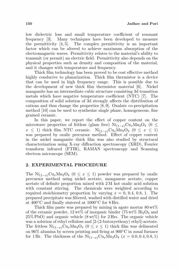
To further explore the doping effect of copper in the fritlessNiMn2O4 thick film, vibration modes have been studied by means ofFTIR and RAMAN spectra measurements because vibration modesare sensitive to substitution. In FTIR spectra (Fig. 3) two strongpeaks were observed around 600 cm−1 and 500 cm−1. This confirmedthe formation of spinel structure. As copper content increases the peakat 605 cm−1 shifts to 600 cm−1. This might be because the valance ofCu is smaller than Ni due to which the force constant of CuO6 aresmaller than NiO6 octahedron [11]. The peak around 510 cm−1 shiftsto 496 cm−1 due to the increase in copper content indicating decreasein frequency since the heavier Cu ions are substituted for Ni.
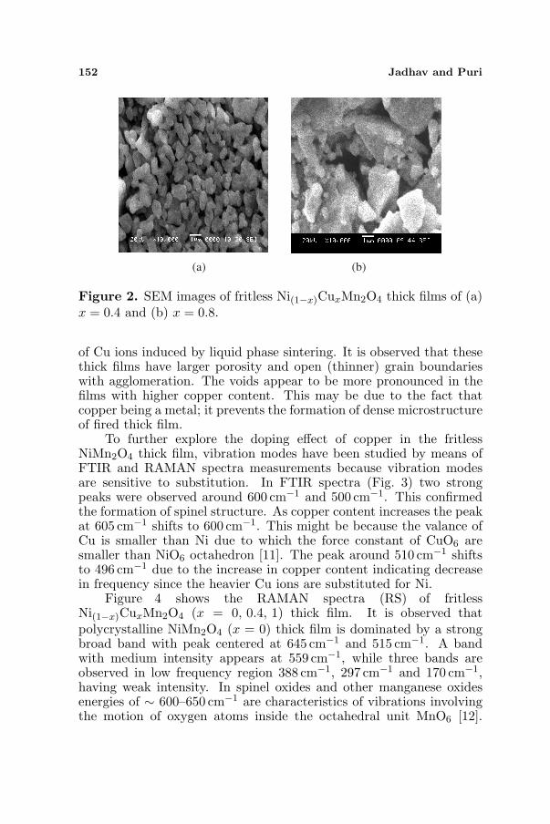
Figure 4 shows the RAMAN spectra (RS) of fritlessNi(1−x)CuxMn2O4 (x = 0, 0.4, 1) thick film. It is observed thatpolycrystalline NiMn2O4 (x = 0) thick film is dominated by a strongbroad band with peak centered at 645 cm−1 and 515 cm−1. A bandwith medium intensity appears at 559 cm−1, while three bands areobserved in low frequency region 388 cm−1, 297 cm−1 and 170 cm−1,having weak intensity. In spinel oxides and other manganese oxidesenergies of ∼ 600–650 cm−1 are characteristics of vibrations involvingthe motion of oxygen atoms inside the octahedral unit MnO6 [12].
Progress In Electromagnetics Research C, Vol. 8, 2009 153
300 400 500 600 700 800
60
5.7
496.7
60
0.7
50
3
60
3
51
0
x=1
x=0.4
x=0.0
cm
Tra
nsm
itta
nce (
a.u
.)
−1
Figure 3. FTIR spectra offritless Ni(1−x)CuxMn2O4 thickfilm.
Ram
an In
tens
ity (
a.u.
)
100 200 300 400 500 600 700 800 900 1000
cm−1
x=0
x=0.4
x=1
170
297
388
559
515
Figure 4. RAMAN spectraof fritless Ni(1−x)CuxMn2O4 thickfilm.
Analysis of the vibrational spectra of NiMn2O4 and CuMn2O4 withFd3m space group yields five modes which are RAMAN activeA1g+Eg+3F2g. The RAMAN band located at about 645 cm−1 isviewed as a symmetric Mn-O stretching vibration of MnO6 group.This high wave number band is assigned to the A1g species in theO7
h spectroscopic symmetry. The RS peak at 297 cm−1 derives fromthe Eg symmetry whereas the peaks located at 170 cm−1, 388 cm−1,559 cm−1 derives from F2g species. Similar spectra have been observedin LiMn2O4 [13]. Dokko et al. [14] have reported that the peakintensity at ∼ 515 cm−1 is sharper due to nickel content and it isattributed to Ni2+-O stretching mode in structure. As copper contentincreases RAMAN spectra shifts towards lower frequency (peaks shownby arrow). At x = 0 it is 645 cm−1, at x = 0.4 it is 636 cm−1
and for x = 1 it is 600 cm−1 which is due to the heavier Cu ionssubstituted for Ni ions. The reduction of the intensity of this mode isdue to the decrease of Jahn-Teller distortions in the averaged structureintroduced by the smaller Cu ions [15] (ionic radii of Cu2+ = 0.70 Aand Ni2+ = 0.78 A) [16].
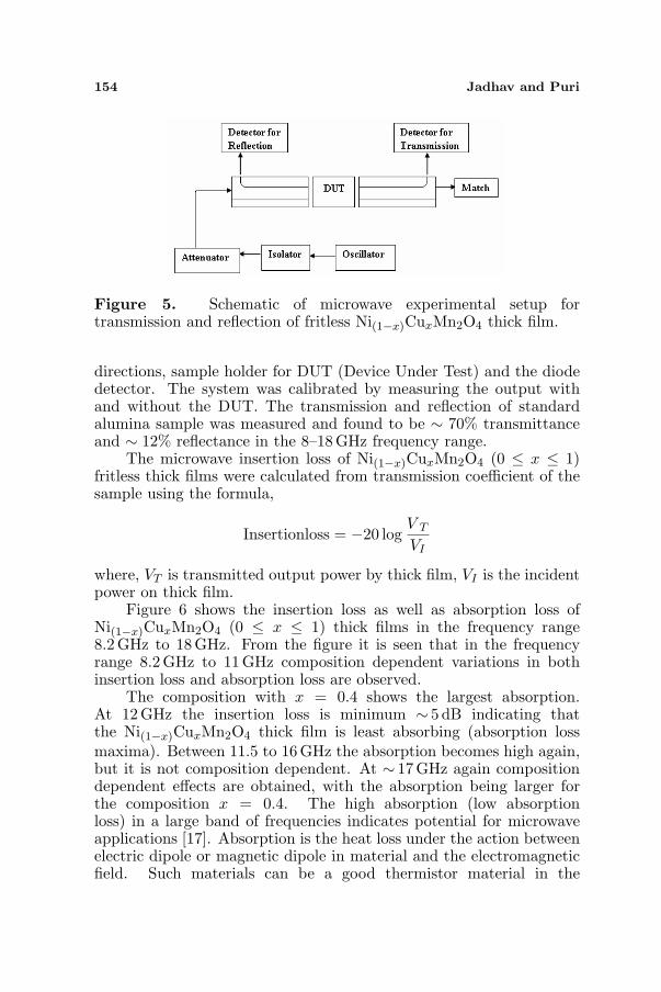
The transmission and reflection of fritless Ni(1−x)CuxMn2O4 (0 ≤x ≤ 1) thick films was measured by the rectangular waveguidereflectometer set up shown in Fig. 5. The microwaves incident onthe device under test were in the frequency range 8GHz to 18GHz.The waveguide reflectometer set up consists of Gunn oscillator,isolator, attenuator, two 3 dB directional couplers connected in reverse
154 Jadhav and Puri
Figure 5. Schematic of microwave experimental setup fortransmission and reflection of fritless Ni(1−x)CuxMn2O4 thick film.
directions, sample holder for DUT (Device Under Test) and the diodedetector. The system was calibrated by measuring the output withand without the DUT. The transmission and reflection of standardalumina sample was measured and found to be ∼ 70% transmittanceand ∼ 12% reflectance in the 8–18 GHz frequency range.
The microwave insertion loss of Ni(1−x)CuxMn2O4 (0 ≤ x ≤ 1)fritless thick films were calculated from transmission coefficient of thesample using the formula,
Insertionloss = −20 logV T
VI
where, VT is transmitted output power by thick film, VI is the incidentpower on thick film.
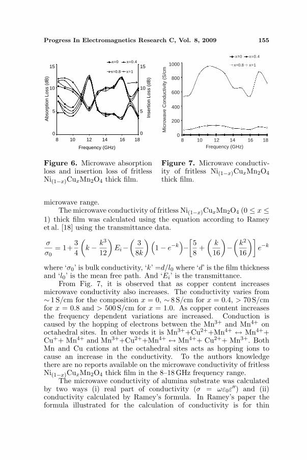
Figure 6 shows the insertion loss as well as absorption loss ofNi(1−x)CuxMn2O4 (0 ≤ x ≤ 1) thick films in the frequency range8.2GHz to 18 GHz. From the figure it is seen that in the frequencyrange 8.2 GHz to 11GHz composition dependent variations in bothinsertion loss and absorption loss are observed.
The composition with x = 0.4 shows the largest absorption.At 12GHz the insertion loss is minimum ∼ 5 dB indicating thatthe Ni(1−x)CuxMn2O4 thick film is least absorbing (absorption lossmaxima). Between 11.5 to 16GHz the absorption becomes high again,but it is not composition dependent. At ∼ 17GHz again compositiondependent effects are obtained, with the absorption being larger forthe composition x = 0.4. The high absorption (low absorptionloss) in a large band of frequencies indicates potential for microwaveapplications [17]. Absorption is the heat loss under the action betweenelectric dipole or magnetic dipole in material and the electromagneticfield. Such materials can be a good thermistor material in the
Progress In Electromagnetics Research C, Vol. 8, 2009 155
15
10
5
0
Inse
rtio
n Lo
ss (
dB)
15
10
5
08 10 12 14 16 18
Frequency (GHz)
x=0 x=0.4
x=0.8 x=1
Abs
orpt
ion
Loss
(dB
)
Figure 6. Microwave absorptionloss and insertion loss of fritlessNi(1−x)CuxMn2O4 thick film.
x=0
x=0.8
x=0.4
x=1
8 10 12 14 16 18Frequency (GHz)
Mic
row
ave
Con
duct
ivity
(S
/cm
1000
800
600
400
200
0
Figure 7. Microwave conductiv-ity of fritless Ni(1−x)CuxMn2O4
thick film.
microwave range.The microwave conductivity of fritless Ni(1−x)CuxMn2O4 (0 ≤ x ≤
1) thick film was calculated using the equation according to Rameyet al. [18] using the transmittance data.
σ
σ0= 1+
34
(k − k3
12
)Ei−
(38k
)(1− e−k
)−
[58
+(
k
16
)−
(k2
16
)]e−k
where ‘σ0’ is bulk conductivity, ‘k’ =d/l0 where ‘d’ is the film thicknessand ‘l0’ is the mean free path. And ‘Ei’ is the transmittance.
From Fig. 7, it is observed that as copper content increasesmicrowave conductivity also increases. The conductivity varies from∼ 1 S/cm for the composition x = 0, ∼ 8 S/cm for x = 0.4, > 70 S/cmfor x = 0.8 and > 500 S/cm for x = 1.0. As copper content increasesthe frequency dependent variations are increased. Conduction iscaused by the hopping of electrons between the Mn3+ and Mn4+ onoctahedral sites. In other words it is Mn3++Cu2++Mn4+ ↔ Mn4++Cu++ Mn4+ and Mn3++Cu2++Mn4+ ↔ Mn4++ Cu2++ Mn3+. BothMn and Cu cations at the octahedral sites acts as hopping ions tocause an increase in the conductivity. To the authors knowledgethere are no reports available on the microwave conductivity of fritlessNi(1−x)CuxMn2O4 thick film in the 8–18GHz frequency range.
The microwave conductivity of alumina substrate was calculatedby two ways (i) real part of conductivity (σ = ωε0ε
′′) and (ii)conductivity calculated by Ramey’s formula. In Ramey’s paper theformula illustrated for the calculation of conductivity is for thin

156 Jadhav and Puri
Figure 8. Microwave conductivity of alumina substrate, where σ1is real part of conductivity (σ = ωε0ε
′′) and σ2 is the conductivitycalculated by Ramey’s formula.
conductor films. But in this paper we applied this formula for astandard dielectric alumina sample for 8–18 GHz frequency range.Comparing both Ramey’s and using dielectric formula, the valuesobtained by both are well in agreement with each other which is shownin Fig. 8. Hence, we applied this standardized method to our dielectricnickel manganite thick films.
The dielectric constant of fritless Ni(1−x)CuxMn2O4 thick film wasmeasured using VSWR measurement setup. The VSWR measurementsetup was almost the same as the waveguide reflectometer setup,instead of two 3 dB directional couplers VSWR slotted section wasused. Initially the slotted section was calibrated with air andalumina. The alumina and manganite thick films acts as a load to thetransmission of the microwaves and microwaves reflected back fromthat load. The positions of the minima of the standing wave werecompared with that of air. As impedance is mismatched, the position ofthe minima is shifted by placing the thick films as load. The reflectioncoefficient was also measured. The Smith chart was used to find thephase change due to the fritless Ni(1−x)CuxMn2O4 (0 ≤ x ≤ 1) thickfilm in the path of microwaves and permittivity measured by using theformula [19].
ε′ =(
1 +∆φλ0
360d
)2
and ε′′ =∆φλ0
√ε′
8.686πd
where ‘∆φ’ is phase difference between incident and reflected waves;‘λ0’ is guided wavelength. And ‘d’ is thickness of the sample.
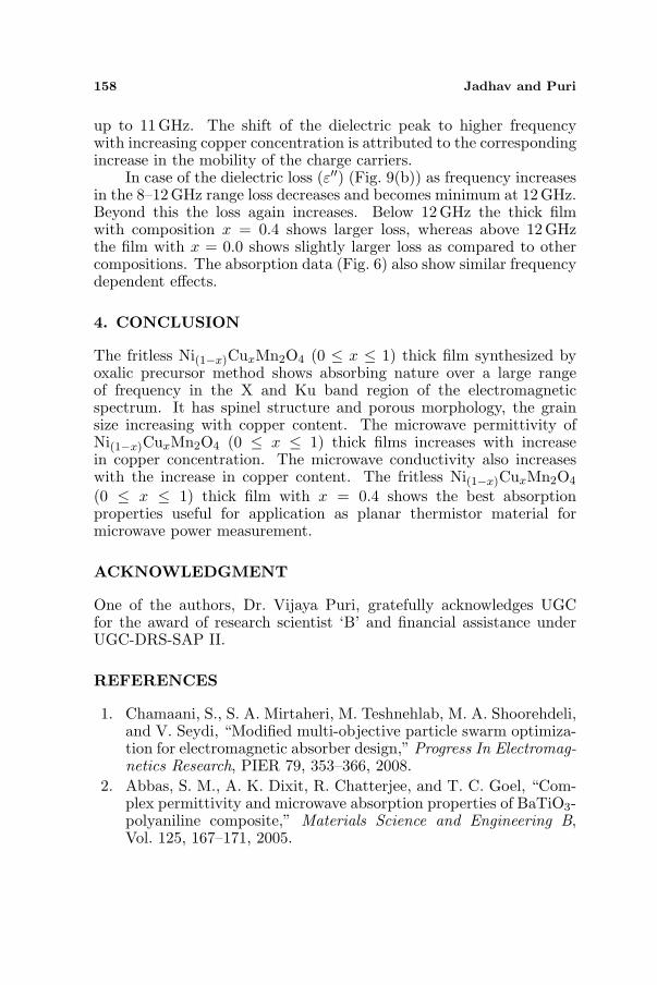
The calculated ε′ and ε′′ are plotted in Figs. 9(a) and (b); it is
Progress In Electromagnetics Research C, Vol. 8, 2009 157
observed that as Cu concentration increases dielectric constant alsoincreases. The value of ε′ lies in the range 6 to 19.5, and ε′′ is inbetween 0.0391 to 0.1875.
x=0 x=0.4
x=0.8 x=1
x=0 x=0.4
x=0.8 x=1
8 10 12 14 16 18
Frequency (GHz)
8 10 12 14 16 18
Frequency (GHz)
(a) (b)
Die
lectr
ic c
onsta
nt (g
)
25
20
15
10
5
0
0.3
0.2
0.1
0
Die
lectr
ic L
oss (ε'')
Figure 9. (a) Microwave dielectric constant of the fritlessNi(1−x)CuxMn2O4 thick film. (b) Microwave dielectric loss of thefritless Ni(1−x)CuxMn2O4 thick film.
The microwave permittivity of Ni(1−x)CuxMn2O4 (0≤ x ≤1)thick film depends on the shape and size of the grains. It is wellknown that as polarization increases dielectric constant also increases,and polarization is affected by structural homogeneity, stoichiometry,density, grain size and porosity [16]. Due to increase in copper contentthe structural homogeneity decreases which may cause a slight increasein polarization.
In fritless Ni(1−x)CuxMn2O4 thick film due to Cu content thegrain size increases (SEM Fig. 2) and anisotropy decreases whichis responsible for the increase in dielectric constant. According toZaki [20] the substitution of Cu ions cause the formation of vacancies,if the formed vacancies are cations then ε′ increases. The decrease inthe intensity of peak 645 cm−1 (Fig. 4) with copper content is dueto Mn-O bond strength in this region being weaker, which resultsin larger polarization and hence higher dielectric constant for highercopper concentration.
From Fig. 9(a), the dielectric constant shows peaking behavior atlower frequency. It is observed that for lower copper concentration(x ≤ 0.4) dielectric constant peak is observed at 10 GHz but whencopper content increases (x ≥ 0.8) it shifts towards higher frequency
158 Jadhav and Puri
up to 11GHz. The shift of the dielectric peak to higher frequencywith increasing copper concentration is attributed to the correspondingincrease in the mobility of the charge carriers.
In case of the dielectric loss (ε′′) (Fig. 9(b)) as frequency increasesin the 8–12GHz range loss decreases and becomes minimum at 12 GHz.Beyond this the loss again increases. Below 12GHz the thick filmwith composition x = 0.4 shows larger loss, whereas above 12 GHzthe film with x = 0.0 shows slightly larger loss as compared to othercompositions. The absorption data (Fig. 6) also show similar frequencydependent effects.
4. CONCLUSION
The fritless Ni(1−x)CuxMn2O4 (0 ≤ x ≤ 1) thick film synthesized byoxalic precursor method shows absorbing nature over a large rangeof frequency in the X and Ku band region of the electromagneticspectrum. It has spinel structure and porous morphology, the grainsize increasing with copper content. The microwave permittivity ofNi(1−x)CuxMn2O4 (0 ≤ x ≤ 1) thick films increases with increasein copper concentration. The microwave conductivity also increaseswith the increase in copper content. The fritless Ni(1−x)CuxMn2O4
(0 ≤ x ≤ 1) thick film with x = 0.4 shows the best absorptionproperties useful for application as planar thermistor material formicrowave power measurement.
ACKNOWLEDGMENT
One of the authors, Dr. Vijaya Puri, gratefully acknowledges UGCfor the award of research scientist ‘B’ and financial assistance underUGC-DRS-SAP II.
REFERENCES
1. Chamaani, S., S. A. Mirtaheri, M. Teshnehlab, M. A. Shoorehdeli,and V. Seydi, “Modified multi-objective particle swarm optimiza-tion for electromagnetic absorber design,” Progress In Electromag-netics Research, PIER 79, 353–366, 2008.
2. Abbas, S. M., A. K. Dixit, R. Chatterjee, and T. C. Goel, “Com-plex permittivity and microwave absorption properties of BaTiO3-polyaniline composite,” Materials Science and Engineering B,Vol. 125, 167–171, 2005.

Progress In Electromagnetics Research C, Vol. 8, 2009 159
3. Zhang, Y. C., Z. X. Yue, X. Qi, B. Li, Z. L. Gui, and L. T. Li,“Microwave dielectric properties of Zn(Nb1−xTax)2O6 ceramics,”Materials Letters, Vol. 58, 1392–1395, 2004.
4. Chou, Y.-H., M.-J. Jeng, Y.-H. Lee, and Y.-G. Jan, “Measurementof RF PCB dielectric properties and losses,” Progress InElectromagnetics Research Letters, Vol. 4, 139–148, 2008.
5. He, X., Z. X. Tang, B. Zhang, and Y. Q. Wu, “A new deembeddingmethod in permittivity measurement of ferroelectric thin filmmaterial,” Progress In Electromagnetics Research Letters, Vol. 3,1–8, 2008.
6. Marie, M., J. Mazzochette, A. H. Feingold, P. Amstutz,R. L. Wahlers, C. Huang, and S. J. Stein, “Thick film variabletemperature variable attenuators,” Proceeding of the 1997 IMPSPhiladelphia Symposium, Vol. 3235, 344–349, 1997.
7. Savic, S. M., M. V. Nikolic, O. S. Aleksic, M. Slankamenac,M. Zivanov, and P. M. Nikolic, “Intrinsic resistivity of sinterednickel manganite vs. powder activation time and density,” Scienceof Sintering, Vol. 40, 27–32, 2008.
8. Verses, A., J. G. Noudem, O. Pery, S. Founez, and G. Bailleul,“Manganese based spinel — Like ceramics with NTC — Typethermistor behavior,” Solid State Ionics, Vol. 178, 423–428, 2007.
9. Park, K., “Structural and electrical properties ofFeMg0.7Cr0.7−xAlxO4 (0 ≤ y ≤ 0.3) thick film NTC ther-mistors,” Journal of European Ceramic Society, Vol. 256,909–914, 2006.
10. Kanade, S. A. and V. Puri, “Properties of thick filmNi0.6Co0.4FeyMn2−yO4: (0≤ y ≤0.5) NTC ceramics,” Journal ofAlloys and Compounds, Vol. 475, 352–355, 2009.
11. Pi, L., X. Xu, and Y. Zhang, “Anomalous transport propertiesof heavily doped polycrystalline La0.825Sr0.175Mn1−xCuxO3,”Physical Review B, Vol. 62, 5667–5672, 2000.
12. Julien, C., M. Massot, S. Rangan, M. Lemal, and D. Guyomard,“Study of structural defects in -MnO2 by Raman spectroscopy,”Journal of Raman Spectroscopy, Vol. 33, 223–228, 2002.
13. Chitra, S., P. Kalyani, T. Mohan, M. Massot, S. Ziolkiewicz,R. Ganandharan, M. Eddrief, and C. Julien, “Physical propertiesof LiMn2O4 spinel prepared at moderate temperature,” Ionics,Vol. 4, 8–15, 1998.
14. Dokko, K., M. Mohamed, N. Anzue, T. Itoh, and I. Uchida,“In situ Raman apectroscopic studies of LiNixMn2−xO4 thin filmcathod materials for lithium ion secondary batteries,” Journal of
160 Jadhav and Puri
Materials Chemistry, Vol. 12, 3688–3693, 2002.15. Li, W. J., B. Zang, and W. Lu, “Structural properties and Raman
spectroscopy of La(2+4x)/3Mn1−xCuxO3 (0 ≤ x ≤ 0.2),” PhysicsLetters A, Vol. 362, 327–330, 2007.
16. Dimri, M., A. Verma, S. Kashyap, D. Dube, O. Thakur, andC. Prakash, “Structural, dielctric and magnetic properties ofNiCuZn ferrite grown by citrate precursour mehod,” MaterialsScience and Engineering B, Vol. 133, 42–48, 2006.
17. Li, G., G. G. Hu, H. D. Zhou, X. J. Fan, and X. G. Li, “Absorptionof microwaves in La1−xSrxMnO3 manganese powders over a widebandwidth,” Journal of Applied Physics, Vol. 90, 5512–5514, 2001.
18. Ramey, R. and T. Lewis, “Properties of thin metal films atmicrowave frequencies,” Journal of Applied Physics, Vol. 39, 1747–1752, 1968.
19. Kim, J. H., K. B. Kim, and S. H. Noh, “New density independentmodel for measurement of grain moisture content using microwavetechniques,” Journal of Electronics Engineering and InformationScience, Vol. 2, 72–78, 1997.
20. Zaki, H. M., “AC conductivity and frequency dependence ofthe dielctric properties for copper doped magnetite,” Physica B,Vol. 363, 232–244, 2005.