microstructured terahertz waveguides - opusopus.bath.ac.uk/43661/3/submitted_version.pdf · the...
TRANSCRIPT

1
Microstructured Terahertz Waveguides
Steven R. Andrews
Department of Physics, University of Bath, Bath BA2 7AY, UK
e-mail: [email protected]
Abstract
Research involving the tetrahertz (THz) part of the electromagnetic spectrum, commonly
taken to be the region between 0.1 and 10 THz (3 mm to 30 µm), has seen rapid growth in
recent years because of the importance of THz radiation as a low energy probe of the optical
properties and dynamics of matter and partly because of emerging real world applications in
areas as diverse as industrial quality control, biosensing and security screening. Despite a
vigorous growth in THz technology, many components and processes taken for granted at
higher and lower frequencies are still in an early stage of development. One example of this is
the use of waveguides to transport or spatially confine radiation. In this review we summarise
progress in developing THz waveguides, paying attention to the role that microstructuring on
a sub-wavelength length scale can play in engineering new capability and the various trade-
offs between loss, bandwidth, group velocity dispersion and spatial confinement.
Key words: Terahertz, far-infrared, waveguide, transmission line, photonic crystal,
microstructure, optical fiber, near field, metamaterial, plasmonics
(Some figures may appear in colour only in the online journal)

2
1. Introduction
Interest in the far-infrared region of the electromagnetic spectrum, which lies between
microwaves and the mid-infrared, has witnessed a renaissance over the last twenty years, as
reflected by its rebranding as the terahertz (THz) part of the spectrum. The development of
technology for accessing this spectral band is strongly motivated by applications in
fundamental science and the quest for higher bandwidth signal processing and new imaging
and sensing modalities [1]. Examples of established or emerging applications include the
characterization of the optical and dynamical properties of materials [2,3], medical imaging
[4], pharmaceutical quality control [5], communications [6] and security screening [7]. The
application to sensing is another important example. Many organic molecules, for example
those in plastic explosives [6], have characteristic vibrational modes at THz frequencies,
whilst important biomolecules such as proteins and nucleic acids have structurally sensitive
broadband dielectric responses. Perhaps the best known application of the latter property is
label free sensing of DNA hybridization with immobilised probe molecules by means of the
change in THz absorption and refractive index [8].
The growth in scientific applications at THz frequencies has been driven in no small part by
the parallel development of ultrafast optical and opto-electronic techniques for generating and
coherently detecting THz radiation and stable, easy to use femtosecond lasers. The usual
operating range of these techniques, collected under the umbrella name Time Domain
Terahertz Spectroscopy (TDTS), lies in the range 0.1 to 5 THz [9]. This range is sometimes
used to describe the THz spectral window although increasingly, the same sort of techniques
are being deployed at frequencies which overlap the mid-infrared, aided by the development
of ever shorter pulse lasers and all-optical generation and detection techniques. In the last few
years, however, it has become clear that cryogenically cooled quasi-CW (continuous wave)
quantum cascade lasers (QCLs), originally developed in the mid-infrared, but now
engineerable with frequencies down to ~2 THz and with peak pulsed powers of up to 1 W
[10,11], will also play an important role in the eventual translation of THz applications from
the research lab to the real world. An impediment to the wider use of all the above technogies
is their size and cost but new technologies are continually being explored and for some
applications, at the lower frequency end of the THz band, cheaper more compact solutions
based on photomixing [12], multimode semiconductor lasers [13] or short pulse
semiconductor lasers [14] might suffice.

3
Although techniques for generating and detecting THz radiation have advanced considerably
in the last decade or so, the development of the associated optical components that one needs
to be able to perform many of the measurements that are taken for granted in other spectral
ranges has not developed as quickly. Examples are high performance polarisers, modulators,
waveplates, detector arrays and waveguides. In this review we attempt to give an overview of
the varied work on developing the latter class of component, with an emphasis on the role that
microstructuring can play in engineering desirable properties. For completeness we also hint
at their applications and summarise the status of what might be thought of as more
conventional structures such as the hollow metal tube and parallel plate waveguide because
these can be adapted or improved by the addition of sub-wavelength-scale features such as
surface texturing or thin dielectric coatings.
The scale invariance of Maxwell’s equations suggests that, if dispersion of the optical
constants of materials can be ignored, successful waveguide concepts at optical and
microwave frequencies should be translatable to the THz region. However, the practicality of
so doing is constrained by the fact that whilst at microwave frequencies, metals behave like
perfect conductors and at optical frequencies there are many excellent low loss dielectrics,
this is not the case at THz frequencies where metals are lossy and only high resistivity single
crystal silicon stands out as as a low absorption material (<0.05 cm-1 over most of the THz
band [15]). The desire for broadband operation (partly for the ubiquitous pulsed techniques
which also require low dispersion) leads to even greater challenges because the desired
spectral bandwidth often spans many octaves.
A large number of waveguide concepts are currently being explored, including hollow metal
tubes, planar transmission lines, metamaterial surfaces and microstructured optical fibers.
This variety reflects the wide range of possible applications such as spectroscopy, endoscopy,
near field imaging, plasma diagnostics, on-chip biosensing and high speed interconnects.
Different applications generally have different requirements, which might involve several
properties chosen from a list including flexibility, small size, low loss, high bandwidth,
strong spatial confinement and low dispersion. The ideal properties are sometimes mutually
exclusive so that compromises must be found and this is aided by the range of possible
approaches on offer.
Although they are well known, it is worth saying a little about the experimental techniques
and theoretical approaches used in the characterization of THz waveguide. The experimental

4
tool of choice is broadband TDTS in which pulsed THz radiation is generated by femtosecond
laser pumping of nonlinear optical crystals or biased photoconductive antennas [8,9].
Coherent detection is achieved by means of a time delayed probe pulse which is used to
sample the THz field in an electro-optic crystal or a photoconductive antenna. The term
coherent used here means that the electric field is measured as a function of pump-probe
delay rather than the intensity. The spectral amplitude and phase of the field can then be
obtained by Fourier transformation of the time domain signal. Figure 1a shows a typical
quasi-optical setup for studying waveguides. In some experiments it is convenient to replace
the lens before the waveguide by a compact transmitter such as a ZnTe crystal [16] or a
photoconductive array [17] or to replace the standard linearly polarised transmitter by one
with radial polarisation [18]. A waveguide transmission measurement, together with a
reference measurement obtained by removing or (preferably) cutting back the waveguide, can
be used to obtain the waveguide attenuation , propagation constant () and, by
differentiation, the group velocity (vg) dispersion (GVD), 2=d(1/vg)/d=d2/d2 which
typically has units of ps/THz/cm.
Fig. 1: (a) Typical time domain spectrometer setup using photoconductive tranmitters and receivers adapted for
studying waveguides. Pump and probe beams derived from the same femtosecond laser and having a variable
time delay between them are used to excite the transmitter and gate the receiver respectively. (b) Example of
modification to allow near field waveguide imaging at the exit face of a waveguide. A photoconductive
transmitter and near field probe are coupled to a femtosecond laser using photonic crystal fiber (PCF) to allow
free positioning [21]. (c) Typical time domain reference signal in setup (a). (d) is the amplitude spectrum of (c)
and shows up to 5 THz of potentially useful bandwidth. (colour online)

5
A typical time domain trace and its amplitude spectrum (without waveguide) are shown in
figures 1c and 1d respectively. The basic setup is often modified to allow near field imaging
of the waveguide output, for example using the configuration shown in figure 1b. Such
imaging can give detailed information about mode structure and mode coupling [16]. The
near field probe in figure 1b might consist of a thin electro-optic crystal with tightly focused
probe beam [19], a photoconductive antenna, with or without an integrated aperture
[16,20,21] or a sharp metal scattering tip in association with a far field detector [22]. The
typical spatial resolution used for waveguide characterization is in the range 10 to 100 µm.
Analytical treatments of waveguide dispersion and attenuation are possible in simple cases or
in certain approximations or limits and can be useful in aiding physical understanding.
Microstructuring usually make direct solution of Maxwell’s equations too complicated but all
of the guides that we discuss can in principle be using commercially available full vectorial
electromagnetic simulation software based, for example, on the finite difference time domain
(FDTD) technique [23]. However, it should be noted that numerical simulations are
frequently computationally expensive. This is because they can require a very large number of
mesh cells if they encompass length scales ranging from the few nm needed to describe the
field penetration into metals to the many cm lengths that might be required to form stable
modes in macroscopic guides or to investigate bend loss. Simplifications and approximations
are therefore usually made. For example, material dispersion might be neglected, the input
and output coupling might not be treated realistically or surface roughness and bulk
inhomogeneity might be ignored. Common approximations are to treat metals as perfect
electrical conductors (PECs) or to use surface impedance boundary conditions. Such
approximations inevitably require that waveguide concepts are also tested experimentally and
this review will emphasise experimental studies more than theoretical ones.
The contents of this paper are arranged as follows. In sections 2, 3 and 4 we summarise work
on what might be thought of as traditional guiding concepts based on metal tubes, parallel
plates and planar transmission lines, highlighting recent innovations. In sections 5 and 6 we
describe THz guiding on metamaterial surfaces and in microstructured optical fibers. In
section 7 we present some conclusions and an outlook for future work. We have not
attempted to exhaustively list every relevant work in such a short review but instead have
tried to select a subset which hopefully provides a flavour of the current status of the field.
The reader might want to rectify any bias or omission by refering to more specialised reviews
that overlap this one to some degree, such as a very early one by Grischkowsky [24], whose

6
group has pioneeered THz waveguide studies, and a recent one on dielectric waveguides by
Atakaramians et al [25].
2. Hollow metal guides
The use of cylindrical and rectangular, hollow metal guides is ubiquitous in the microwave
region. The first TDTS studies of similar structures were made by Grischkowsky’s group
[26,27] in a set-up like that shown in figure 1a. For small (few mm or less) diameters the
modes closely resemble the well known analytical solutions for guides with perfectly
conducting walls [28]. These solutions are of two types: transverse electric (TEnm) with no
axial electric field component and transverse magnetic (TMnm) with no axial magnetic field
component. Here, n and m are integers that characterise the guided mode. Optically or
optoelectronically generated broadband THz pulses generally have spectra spanning 4 to 6
octaves (see figure 1d) and therefore usually encompass the cut-off frequencies of a number
of modes. However, the coupling coefficients (proportional to the square of spatial field
overlap integrals) to the usual linearly polarised TEM00 Gaussian input beam are small for all
but a few of the lowest order ones. In guides with tranverse internal dimensions up to few mm
or more. linearly polarised beams are experimentally found to couple predominantly to the
TE11 and to a lesser extent the TE12 and TM11 modes of hollow circular guides and the TE10
and TM12 modes of rectangular guides, in accord with the calculated overlap integrals [27]. In
a circular guide, the lowest loss mode is TE01 which has essentially zero field at the metal
surface, but it cannot couple to linearly polarised radiation because it has azimuthal
symmetry.
All modes have low frequency cut-offs with the propagation constant above cut-off described
by
mn ko 1fc,mn
2
f 2, [1]
where for circular guides fc,mn =cmn/(2a) is the cut-off frequency of the TMmn or TEmn mode,
a is the radius and mn is nth non-vanishing root of the mth order Bessel function Jm, or its
derivative Jm , respectively [28].

7
The effect of transmission through a 4 mm long, 280 µm inner diameter, stainless steel
waveguide (hypodermic tube) on a single cycle-like THz pulse is shown in figure 2 [26]. A
sub-ps input pulse is broadened to more than 5 ps and is negatively chirped (high frequencies
arrive earlier than low frequencies, 2<0) because of the dispersion associated with several
mode cut-offs. The spectrum shows oscillatory structure characteristic of multimode
interference. At 1 THz the power absorption coefficient was measured to be 0.7 cm-1 (~3
dB/cm). To put this into context, this is significantly better than planar transmission lines at
the same frequency but a lot worse than can be obtained with the dielectric-lined metal tubes
or polymer fibers. These other types of guide are discussed later. The GVD of the TE11 mode
can be found using equation 1. At 1.5 THz, which is about 0.9 THz above cut-off, the GVD is
estimated to be -11 ps/THz/cm, a value roughly consistent with the pulse broadening and
chirp seen in figure 2a.
Fig.2: (a) Measured THz pulse (dots) transmitted through a 4-mm-long 280 µm diameter, stainless-steel
waveguide. (b) Amplitude spectrum (dots) of the measured transmitted pulse. The solid curves are the theoretical
predictions for coupling to a sum of the TE11 (77%, cut-off at 0.65 THz), TM11 (20%, 1.31 THz) and TE12 (3%,
1.81 THz) modes. The insets show an expanded scale. Reproduced with permission from [26]. Copyright 1999
The Optical Society of America.
Above the cut-off frequency, the modal power attenuation due to Ohmic loss scales as Rs/a
where Rs=√(fo/) is the characteristic surface resistance and is the conductivity. The
attenuation coefficient of the experimentally dominant modes in the a<< limit is given by
[28]

8
( f ) 2
a(ko
)o f
. [2]
In a 280 µm diameter stainless steel guide, the loss estimated from equation 2 is ~ 2.7 dB/cm
at 1 THz for stainless steel, in rough agreement with experiment [26]. For copper, the best
reflector at THz frequencies, the higher conductivity leads to a lower estimated loss of ~ 0.4
dB/cm.
A fact not generally appreciated, although discussed in detail by Kato and Miyagi [29], is that
as the radius of a circular guide is increased the TE1n and TM1n modes, which can couple to
linearly polarised radiation, undergo a transformation into hybrid modes which possess all
field components. For example, the TE12 mode gradually evolves into the hybrid EH11 mode
and TM11 evolves into HE11. The transformation becomes noticeable when a/ reaches aa
value of ~100, as illustrated in figure 3. A similar picture holds for rectangular metal guides.
Such drastic mode transformations do not occur in hollow core dielectric guides.
Fig. 3: Top: rough sketch of electric field lines for the usually dominant TE11 mode of a cylindrical metal tube
(for a/<10). Bottom: Transformation of the TM11 mode into the hybrid HE11 mode as a/ is increased from 10
to 100 to 1000 [29].
It turns out that the HE11 mode in hollow metal guides has some very useful properties,
namely the field essentially vanishes at the boundary and the field is polarised in one
direction. This gives rise to low Ohmic loss propagation with weak coupling to other modes
and high coupling efficiency (>95%) to linearly polarised free space TEM00-like beams. In
the case of circular guides, the attenuation of the HE11 mode scales with frequency and core

9
radius as √f/(f2a3) [29,30] compared with the √f/a behaviour of all other modes except for
those which also have vanishing field at the metal boundary, such as the azimuthally polarised
TE0m. This makes it particularly attractive at THz frequencies where powers are usually low
and Ohmic loss can be a serious limitation.
In a circular guide the cross-over from TM11 to HE11 character takes place when a >Z/(kZl)
where Z is the wave impedance of the medium filling the guide, k is the wavevector and Zl =–
Ez/ is the longitudinal surface impedance [31]. The coordinates z and refer to the
propagation axis and tangent to the guide inner surface perpendicular to z. For a smooth wall
Zl ~(1+j)Rs so that at 1 THz a copper guide radius larger than 5 cm is required to support a
predominantly HE11 character mode, which is far too large to be practical. Fortunately, the
radius required can be dramatically reduced by increasing the impedance of the inner surface
of the guide. Two alternative approaches to so doing are to create a periodic corrugation or to
apply a thin dielectric coating. At low THz frequencies (<0.5 THz), oversized circular metal
guides with a corrugated internal surface have shown HE11 losses as low as 0.01 dB/m [32].
Such performance is attractive for applications requiring long propagation lengths and high
power transport such as electron cyclotron resonance plasma diagnostics in fusion research
and dynamic nuclear polarization magnetic resonance [32]. The corrugations typically have a
pitch p ~ /3 and depth h~/4. The upper frequency defining the low loss transmission band is
determined by p and the ‘tooth’ width and the lower frequency by h. The length scale of the
structuring makes the fabrication of such guides difficult at THz frequencies although they are
commercially available at a few hundred GHz. A possible route to simplifying fabrication
suggested recently is to stack rings with alternately large and small inner diameters inside a
sleeve [33].
Another approach to improving the attenuation of the bare metal tube is to coat the inside
surface with an impedance transforming dielectric with thickness chosen to sustain the HE11
mode, a technology first developed for the mid infrared. The optimium coating thickness is
only a small fraction of a wavelength and for a low loss dielectric of index nd can can be
approximated by [34]
d
2 nd2 1
tan1 nd nd2 1
1/4
. [3]

10
Polystrene (nd=1.6) is an easily applied coating material with reasonable loss characteristics
(10 dB/cm at 3 THz [35]) for this application. For this material equation 3 gives an optimum
thickness of 18 µm (or a little less if taking account of dielectric loss) at 2 THz. For such a
thin layer the field fraction in the dielectric is small enough that the effect of the coating on
attenuation and dispersion can be neglected to a first appoximation. The power attenuation in
the ka>>1 limit is then given by [36]
nm unm
2
22
a3
n
n2 2
1
nd2
nd2 1
[4]
where unm is the mth root of the Bessel function Jn-1 and the refractive index of the metal is
n+j. For high conductivity metals such as Cu or Ag, n/(n2+2) in equation 4 is ~10-3 at 1
THz [37]. For a silver tube with a=1 mm, the attenuation calculated using equation 4 is ~0.1
dB/m at 2 THz. The measured attenuation for Ag/polystyrene tubes of a few mm diameter at
the same frequency has been reported to be ~1 dB/m near 2 THz [34] which is higher than
predicted above although the experimental parameters are not strictly in the ka>>1 limit and
no account was been taken of the effects of atmospheric and dielectric absorption and coating
non-uniformity or roughness which might affect experiments. Experimentally, uncoated tubes
are found to have an order of magnitude larger loss than coated ones of the same diameter
[38], roughly as expected from equations 2 and 4. Apart from its relatively low loss, the
dielectric coated tube also has the attractive feature that both metal and dielectric films can be
deposited inside thin wall polymer tubes using liquid phase chemistry techniques so that it is
possible to manufacture flexible guides [38].

11
Fig.4: (a) Bottom panel: spatial electric field Ex distribution at t = 0 measured at the output of a dielectric coated
waveguide using a terahertz near-field probe; top panel: the corresponding space-time map showing the pulse
waveform as a function of position along the x-axis. (b) Similar measurements on a waveguide with the same
dimensions but without the dielectric layer. (c) Space-time maps showing temporal distribution of the electric
field amplitude at the waveguide output for different frequencies around the pulse peak frequency. Inset: mode
profiles measured at time window delays A and B showing the HE11 mode near zero delay and a superposition of
TE11 and HE12 at a delay of 4.8 ps. Reproduced with permission from [16]. Copyright 2009 The Optical Society
of America. (colour online)
Some of the properties of the dielectric lined, circular metal tube have been confirmed using
near field THz imaging [16] and these particular studies give a good idea of the usefulness of
such techniques for waveguide characterisation. Figures 4a and 4b show near field images
100 µm beyond the output ends of 13 cm long, 1.7 mm inner diameter, silver wall guides
with and without a dielectric coating respectively. The reduction in field at the metal surface
in the coated case is clearly evident. Figure 4c illustrates how the mode composition can be
deduced from field maps at different time delays and also shows the relatively high group
velocity and low GVD of the HE11 mode which is localised near zero delay. Using equation 1,
we calculate the GVD at 2 THz to be -0.075 ps/THz/cm for this structure, which is consistent
with experiment. The GVD increases rapidly as the HE11 cut-off frequency at 0.14 THz is
approached and is -0.60 ps/THz/cm at 1 THz.
Another close relation of the metal tube guide is the coaxial guide which has an additional
centre conductor and supports a TEM radially polarised mode with no cut-off and therefore
potentially low dispersion. This has been studied experimentally at THz frequencies [39] but

12
it is difficult to efficiently couple free space beams to a radially polarised mode and the
dielectric neccessary to support the centre conductor in practical structures would create
additional loss and dispersion. Other configurations which support TEM modes and couple
much more efficiently to linearly polarised free space beams are two parallel wires and two
parallel plates. The parallel plate is particularly important and is discussed at length in section
3.
3. Parallel and tapered plates
An alternative approach to the two dimensional (2D) confinement of metal tubes which is
particularly appealing for use with broadband THz pulses is the one dimensional (1D)
confinement offered by the parallel metal plate guide (PPWG). For input polarisation
perpenducular to the plates, only coupling to TMn modes is possible and these have cut-offs at
fc=nc/2h where h is the plate separation. For small enough h that f1 is larger than the pulse
bandwidth, a PPWG can support only the fundamental TMo (TEM) mode which has a
uniform electric field perpendicular to the plates (in the PEC approximation) together with
impedance matching to free space. Very efficient coupling to a TEM00 free space beam can
therefore be achieved using simple quasi-optical components such as hyper-hemi-cylindrical
silicon lenses. Because the TEM mode has no cut-off the GVD is exceptionally small (zero
for PEC plates, slightly positive for real metal ones). This makes it extremely attractive for
time domain studies because it can support broadband pulse propagation with almost no
distortion [40]. Another very important application of the PPWG is to the construction of THz
QCL ridge waveguides. Here, one of the plates is a thin metal layer deposited on top of the
semiconductor gain medium whilst the other might be an underlying, thin, highly doped
semiconductor layer with plasma frequency well above that of the laser frequency [10].
The power attenuation coefficient of the PPWG is given by [28]
TEM ( f ) 2
h
o f
. [5]
For Cu plates with h=100 µm, equation 5 gives ~0.14 cm-1 (61 dB/m) at 1 THz, in
reasonable agreement with experiment [40]. This value of h is the maximum that allows
single mode TEM operation with a 3 THz bandwidth. The TM1 mode has a cut-off at 1.5 THz
but an even symmetry input field does not couple to this odd symmetry mode. When using
equation 5 it needs to be appreciated that metal surfaces or thin evaporated metal layers might

13
have lower THz conductivity than bulk metals [41]. Another fact that needs to be taken into
account in principle is that the TEM mode of the PPWG evolves into a mode with surface
plasmon-polariton (SPP) character on the two plates when h becomes very large compared
with the wavelength. This effect can be expected to become noticeable when h/>100, in an
analogous way to the mode transformations seen in hollow metal guides described in section
2. The relevance of SPPs to THz guiding is discussed at length in section 5.
A number of useful modifications to the PPWG are possible. For example, the plates can be
curved to make h smaller in the transverse direction so as to limit lateral spread of the guided
mode or an adiabatic longitudinal reduction in h can be used to improve coupling into a
section of guide with very small plate separation. The latter is important because PPWGs can
be used for sensitive spectroscopic sensing of small quantities of material if the plates are
very close together. For example, Zhang and Grischkowsky [42] were able to detect the
presence of water layers as thin as 20 nm in a 50 µm thick, 6.35 cm long Cu PPWG. Mendis
and Grischkowsky [43] have also explored a flexible PPWG as a possible THz interconect.
Another variant is the slot guide, which can be thought of as a narrow plate version of the
PPWG which support a TEM mode with the benefit of transverse confinement. Wächter et al
[17] have verified the very low loss and dispersion of a 270 µm wide slot between 300 µm
thick metallised silicon plates using a minimally invasive photoconductive near field probe
which was scanned along the propagation axis in the region of the fringing field. A similar
approach has been used to characterise porous THz fibers (see section 5) by studying the
evolution of the evanescent field with propagation [44].
A more complicated modification to the PPWG is to etch a periodic array of grooves on one
or both internal surfaces to create a Bragg filter which can be used for sensitive measurements
of changes in refractive index or absorption of material placed in the waveguide by
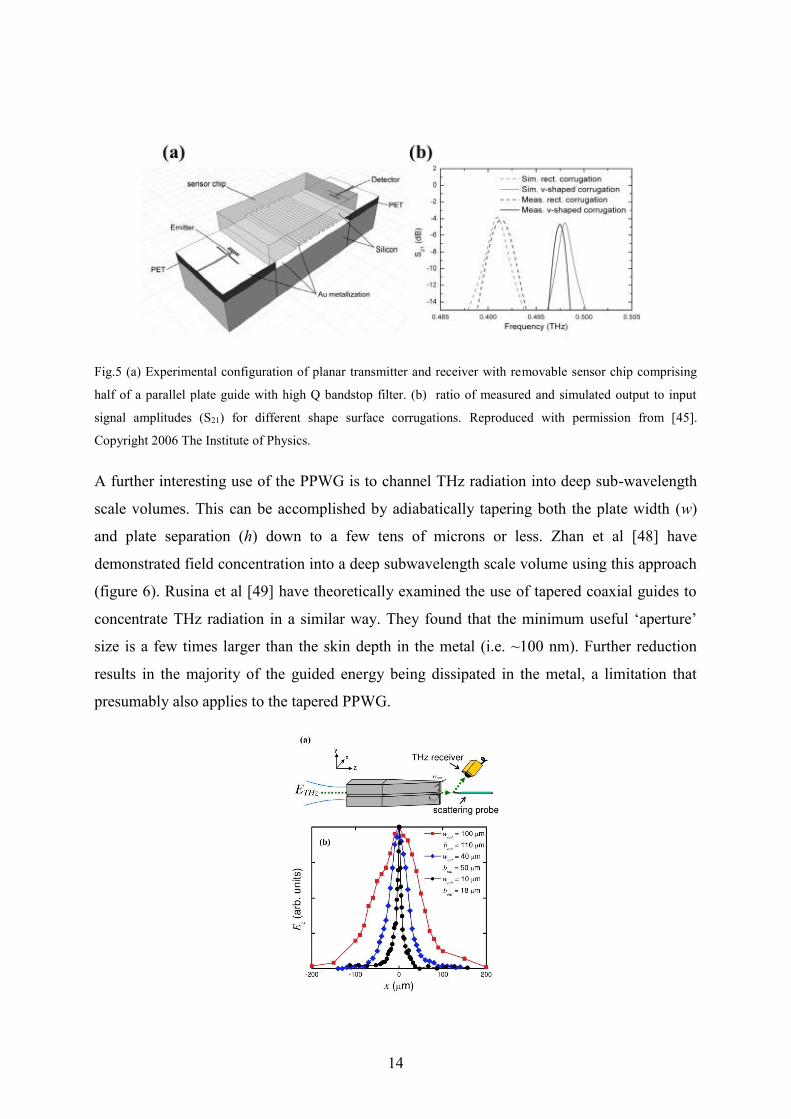
monitoring spectral detuning. Nagel et al [45] showed that a very high Q factor stop band can
be engineered by corrugating just one surface (figure 5). The Q factor of ~500 that they
measured at 0.5 THz is an order of magnitude higher than so far achieved with thin film
microstrip ring resonators based on the guiding technology descibed in section 4. A driving
force behind the work of this group was the search for a sensitive, cheap and disposable
device for marker-free biomolecule detection on functionalised surfaces. Coupled cavities
[46] and 2D photonic crystals [47] have also been integrated with PPWGs but the Q factors
achieved have so far been much lower.
14
Fig.5 (a) Experimental configuration of planar transmitter and receiver with removable sensor chip comprising
half of a parallel plate guide with high Q bandstop filter. (b) ratio of measured and simulated output to input
signal amplitudes (S21) for different shape surface corrugations. Reproduced with permission from [45].
Copyright 2006 The Institute of Physics.
A further interesting use of the PPWG is to channel THz radiation into deep sub-wavelength
scale volumes. This can be accomplished by adiabatically tapering both the plate width (w)
and plate separation (h) down to a few tens of microns or less. Zhan et al [48] have
demonstrated field concentration into a deep subwavelength scale volume using this approach
(figure 6). Rusina et al [49] have theoretically examined the use of tapered coaxial guides to
concentrate THz radiation in a similar way. They found that the minimum useful ‘aperture’
size is a few times larger than the skin depth in the metal (i.e. ~100 nm). Further reduction
results in the majority of the guided energy being dissipated in the metal, a limitation that
presumably also applies to the tapered PPWG.

15
Fig. 6: (a) Experimental arrangement for near field probing of Ez at the exit of a tapered PPWG. (b) Normalized
line scans at the output of a tapered PPWG in close proximity to the edge of one plate where the axial field
component is large. The line scan along the x-axis shows the degree of localization of the THz field at the output
face for different values of plate width wout and plate separation bout. Using the peak spectral component (0.115
THz) of the broadband THz pulse, the narrowest curve corresponds to a localization length of 260 along x. (a)
and (b) reproduced with permission from [48]. Copyright 2010 The Optical Society of America. (colour online)
Although the TEM mode is the one most commonly associated with the PPWG, the TE1
mode, which has electric field parallel to the plates also has some very useful properties, as
pointed out by Mendis and Mittleman [50]. The TE1 cut-off for a plate sep of 5 mm is 30 GHz
which is well below the usual range of TDTS so that dispersion can be effectively ignored.
Unlike the TEM mode, the field is very small at the metal boundaries and this results in a
remarkable ultralow loss. The power attenuation is given by [28]
TE ( f ) 4
h
fc2
f 2
o f
(1 fc2 / f 2 )
. [6]
Using equation 6 we find that the attenuation for a 5 mm copper plate separation is only 2.6
dB/km at 1 THz compared with 1.5 dB/m for the TEM mode at the same h calculated using
equation 5. This can be qualitatively understood by the fact that grazing incidence s-polarised
waves are more strongly reflected than p–polarised ones at a metal surface. The attenuation of
the TE1 mode decreases with increasing frequency in a similar manner to the HE11 mode of a
dielectric coated circular metal guide, which is very different to the case of the TEM mode
where the attenuation increases with frequency. Mendis and Mittleman [51] have shown that
the TE1 mode in PPWGs can be exploited in a variety of potentially useful devices such as
refractive index sensors (by integrating simple cavities), filters and lenses.
4. Planar transmission lines
Some of the earliest guides studied at THz frequencies were based on 3 terminal co-planar
waveguides (CPW) and 2 terminal microstrip (MS) and co-planar stripline (CPS) similar to
those used at microwave frequencies except for smaller dimensions and different choice of
substrate. Figure 7 illustrates the common designs. Work on studying quasi-TEM pulse
propagation in such transmission lines using ultrafast optical techniques was instrumental in
the development of TDTS in the 1980s and transmission lines continue to be used in
photoconductive THz transmitters and receivers and studied for “on-chip” applications like
signal processing and sensing [52,53]. Because of strong attenuation and dispersion the

16
propagation distances are typically only a few mm and the bandwidth struggles to exceed ~2
THz. State of the art attenuation currently appears to be in the range 2-5 dB/mm near 1 THz
[54-57]. The main loss mechanisms are Ohmic (increases as √f), dielectric (usually faster than
f) and radiation (f3) [58]. Radiation in the form of an electromagnetic shock wave, occurs
when an electrical pulse and its associated multipolar electric field distribution propagates
faster than the phase velocity in the dielectric [59]. This Cherenkov effect is a direct result of
the dielectric mismatch beween the substrate and air. One of the main developments in the
last decade has been to reduce radiation loss by building lines on very thin and low
permittivity polymer substrates [54,60] such as BCB (benzocyclobutene) and polypropylene
and by using smaller and more closely spaced tracks. The use of quadrupole electric pulses
(which have a smaller radiation rate than the usual dipolar pulses) on three parallel tracks was
suggested by McGowan et al [55] but has not been widely exploited so far. With careful
optimisation, all of the designs shown in figure 7a seem capable of roughly similar
performance and it appears to be an open question as to whether there is a ‘best’ transmission
line [56,57]. The choice tends to be based on application specific considerations such as the
extent of the evanescent field, ease of integration and impedance matching constraints.
The attractive features of transmission lines for applications are the small size and planar
geometry which makes them compatible with chemical or biochemical sensing of small
samples, monolithic integration with filters and photoconductive THz transmitters and
detectors and operation at cryogenic temperatures [45, 61]. Photoswitch integration is
generally performed by epitaxial lift off of a ~1 µm thick low temperature (LT) GaAs film
from its GaAs substrate, a process involving dissolution of a sacrificial, intermediate layer of
AlAs, followed by van der Waal’s bonding to the transmission line chip. Apart from the lift
off and reattachment steps, which are rather labour intensive, they are easy to make using
standard semiconductor microfabrication techniques. Sensing is based on loading resonators
with a material of interest and monitoring the spectral detuning due to changes in absorption
and refractive index. With appropriate filtering to remove signal reflections, resolution of a
few GHz is possible. Sensing is also possible at multiple frequencies using arrays of filters
[61].
17
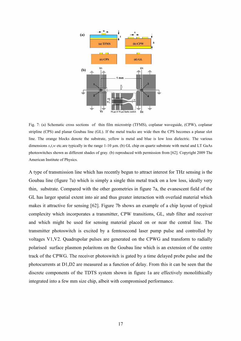
Fig. 7: (a) Schematic cross sections of thin film microstrip (TFMS), coplanar waveguide, (CPW), coplanar
stripline (CPS) and planar Goubau line (GL). If the metal tracks are wide then the CPS becomes a planar slot
line. The orange blocks denote the substrate, yellow is metal and blue is low loss dielectric. The various
dimensions s,t,w etc.are typically in the range 1-10 µm. (b) GL chip on quartz substrate with metal and LT GaAs
photoswitches shown as different shades of gray. (b) reproduced with permission from [62]. Copyright 2009 The
American Institute of Physics.
A type of transmission line which has recently begun to attract interest for THz sensing is the
Goubau line (figure 7a) which is simply a single thin metal track on a low loss, ideally very
thin, substrate. Compared with the other geometries in figure 7a, the evanescent field of the
GL has larger spatial extent into air and thus greater interaction with overlaid material which
makes it attractive for sensing [62]. Figure 7b shows an example of a chip layout of typical
complexity which incorporates a transmitter, CPW transitions, GL, stub filter and receiver
and which might be used for sensing material placed on or near the central line. The
transmitter photoswitch is excited by a femtosecond laser pump pulse and controlled by
voltages V1,V2. Quadrupolar pulses are generated on the CPWG and transform to radially
polarised surface plasmon polaritons on the Goubau line which is an extension of the centre
track of the CPWG. The receiver photoswitch is gated by a time delayed probe pulse and the
photocurrents at D1,D2 are measured as a function of delay. From this it can be seen that the
discrete components of the TDTS system shown in figure 1a are effectively monolithically
integrated into a few mm size chip, albeit with compromised performance.

18
5. Surface waveguiding and metamaterials
Coupling between light and the collective oscillations of the electron plasma at a conductor-
dielectric interface gives rise to hybrid, quasi-TEM propagating surface modes called surface
plasmon-polaritons (SPPs) [63]. The motion of the electronic system exhibits a phase lag with
respect to the driving electromagnetic field resulting in reduced phase and group velocities of
the SPP. This gives rise to strong field localization at the surface at frequencies which are an
appreciable fraction of the (uncoupled) surface plasmon frequency, which for metals
generally lies in the ultraviolet. At optical frequencies, SPPs have fields which decay
exponentially with distance from a metal-dielectric interface on length scales of order a few
10’s of nm in the metal and a fraction of the free space wavelength in the dielectric. Because
the fields are strongly enhanced and confined on a few hundred nm scale, such modes have
found applications in magneto-optic data storage, chemical sensing and near field microscopy
and spectroscopy [63].
Fig. 8 Calculated SPP dispersion curves for silver and n-type InSb surfaces in air. With increasing propagation
constant the SPP frequency asymptotically approaches the surface plasmon frequency, which for a metal is √2
times smaller than the bulk plasma frequency.
The SPP propagation constant is given by
kdm
m d [7]
where kd is the wavevector in the dielectric and m,and d are the complex dielectric
constants of the conductor and dielectric. An essential requirement for the existence of SPPs
is that the real parts of m and d are of opposite sign. Equation 7 is plotted in figure 8 for two
conductors with very different plasma frequencies, the metal Ag and the semiconductor InSb.

19
Surface waves have >kd where kd is the wavevector in the dielectric and thus have
dispersion curves below the light cone in figure 8. This indicates that coupling to free space
beams requires some method of phase matching. Furthermore, the SPP decay length into the
dielectric is equal to 1 / 2 kd2 so that strongly bound SPPs lie further below the light cone
than weakly bound ones. Figure 8 therefore shows that SPPs become increasingly delocalised
as the frequency is reduced below that of the surface plasmon. In the far infrared and
microwave regions, metals support electromagnetic surface waves, but when so far below the
surface plasmon resonance they resemble perfect conductors and the evanescent field
penetrates very little into the surface and extends a large distance (>>) into the dielectric.
Let us consider a copper surface as a specific example. Using experimental values for the real
and imaginary parts of the dielectric constant at 1 THz [37], the propagation length is found to
several hundred metres and the exponential field decay lengths into air and metal are ~20 cm
and 65 nm respectively. Such extended quasi-TEM surface modes are known as Zenneck
waves on flat surfaces and have been studied at THz frequencies where they resemble grazing
incidence light fields or surface currents more than SPPs in the visible [64,65].
The much lower carrier densities of doped semiconductors compared with metals gives rise to
intrinsic plasma frequencies in the THz range, with associated wavelength-scale decay lengths
into air, as indicated in figure 8. However, even high mobility materials such as InSb are
relatively lossy and engineering opportunities are limited. There is, however, an alternative
way of confining electromagnetic waves to surfaces at THz frequencies. Any sub-wavelength-
scale metal surface structure, such as holes or grooves, can enhance the binding of surface
waves, as discussed some time ago by Goubau [66] and Mills and Maradudin [67].
Physically, the enhanced binding arises because of greater penetration of the field into an
effective surface layer. From a microscopic rather than effective medium viewpoint, the
evanescent field is associated with ‘cavities’ in the surface that are below cut-off. More
recently, the concept was generalised by Pendry and co-workers [68], who introduced the idea
of plasmonic metamaterials with surface waves mimicking some of the properties of SPPs but
with effective plasma frequencies entirely determined by geometry. Indeed the metal could in
principle be a perfect conductor which does not support SPPs at all. For brevity we will refer
to what Pendry et al [68] called ‘spoof’ SPPs as S-SPPs.
Metamaterials are generally structured on a sub-wavelength scale, in contrast to photonic
crystals where the periodicity is on the scale of the wavelength. They are being intensively

20
explored for exotic applications such as imaging with resolution below the diffraction limit
[69], and electromagnetic cloaking [70] but here we will concern ourselves only with simpler
‘meta-surfaces’ relevant to S-SPP waveguiding and which provide a functionality
intermediate between that offered by the approaches described in sections 3 and 4.
Fig. 9: Schematic of copper meta-surface structure. a=66 µm, h=58 µm, d=100 µm. (b) S-SPP dispersion curve
for structure in (a) near the Brillouin zone boundary. Green curve shows light line, red shows modal expansion
calculation and blue points show FDTD calculation. Reproduced with permission from [72]. Copyright 2008
Nature.
Following an early CW investigation of THz guiding on a perforated metal sheet by Ulrich
and Tacke [71], S-SPPs on a metamaterial surface comprising an array of square blind holes
in a copper sheet was studied in detail by Williams et al using TDTS [72]. Typical dimensions
and corresponding theoretical dispersion curve are shown in figure 9. The experimental
geometry and electron micrographs of the structure of figure 9a are shown in figure 10a. This
type of structure can be made by photolithographic patterning of thick, epoxy-based
photoresists followed by conformal metal coating using techniques such as catalytically
assisted deposition from the liquid phase. In the experiment, diffraction at metal edges (h1
and h2 in Fig 10a) was used to facilitate phased matched coupling between the S-SPP and a
free space beam. Wavelength-scale out of plane confinement was observed over an octave
range below the Brillouin zone boundary. The degree of confinement was studied using an
adjustable height intermediate aperture (h3) in measurements such as those shown in figure
10b. For example, the amplitude decay length was found to be ~1.3 at 1.3 THz and ~3 at
0.4 THz. These values are hundreds of times smaller than expected for a flat, bare metal

21
surface. The propagation loss near the band edge was estimated to be 1-2 dB/cm, reflecting
the inverse relationship between Ohmic loss and confinement.
Fig. 10: (a) Electron micrograph of a copper meta-surface and schematic of experimental arrangement for
studying S-SPP propagation. (b) Detected signal spectra after propagation 29 mm between apertures 1 and 2
through an intermediate aperture of height h3. The vertical bar indicates the zone boundary cut-off. Reproduced
with permission from [72]. Copyright 2008 Nature. (colour online)
In the case of air filled holes, the cavity resonances in a periodic structure all lie above the
band edge and cannot be accessed experimentally. The periodicity then determines the cut-off
frequency at which S-SPPs form standing waves and above which they cannot propagate.
Whilst effective to a certain degree, this approach does not lend itself to guiding over a large
frequency range or give access to the deeper sub-wavelength-scale field confinement that is in
principle possible close to cavity cut-offs. One way of overcoming these problems is to lower
the cavity cut-off frequency below the band edge by filling the holes with a dielectric having a
refractive index significantly larger than (/a)0.5 where is the period and a is the lateral hole
dimension. A more versatile approach is to change the hole geometry, for example from
square or circular to rectangular or annular where now the hole depth rather than in-plane
dimension controls the cavity cut-off frequency. As an example of this, Williams et al [73]
studied guiding on a copper surface decorated with an array of annular grooves (figures 11a
and 11b) in the more efficient end-fire coupling configuration shown in figure 11c. The
dispersion curves in figures 11d and 11e show that there are two guided modes with the lower
frequency one having a cut-off determined by the dimensions of the annular cavity and the
higher one by the array periodicity. The spectra after THz pulse propagation by 40 mm are
shown in figure 12a and reveal dual band guiding over a broad frequency range. Both guided

22
modes are confined to within a wavelength of the surface, as shown by the near field
measurements in figures 12b and 12c. As is the case in most experiments of this type,
numerical simulations provide a good description of the experimentally observed behaviour.
as shown in figures 12a and 12c.
Fig. 11: (a) Electron micrograph of annular groove metamaterial. (b) Cross section of (a) showing vertical
sidewalls. (c) The experimental geometry for efficiently launching and detecting S-SPPs using hyper-hemi-
cylindrical silicon lenses. (d) Calculated dispersion curves. The insets show maps of the absolute electric field
strength 1 μm above the surface of a unit cell at the TEM (upper left) and TE11 (lower right) cut-off frequencies.
(e) Measured (from spectral phase) and calculated (modal expansion) deviation of dispersion curves from the
light line. Reproduced with permission from [73]. Copyright 2008 American Institute of Physics. (colour online)
Fig. 12: (a) Comparison of calculated (FDTD, solid curve) and measured (points) near field spectra for the
annular groove metamaterial waveguide at a point 100 µm above the surface and 40 µm beyond the output end.
b) Spectral amplitude versus z map in same x plane as (a). Blue is minimum and red is maximum amplitude.
The position of the sample surface is shown by the dashed line. (c) Measured (points, 0.9 THz) and calculated
(curves) field amplitude versus height above the surface at the same x value as (a). The computed field decay
into air is quite sensitive to frequency. Reproduced with permission from [21]. Copyright 2013 American
Institute of Physics. (colour online)

23
An advantage of the meta-surface concept yet to be fully explored is that further functionality
can be engineered. For example, tailoring the transverse guide structure by removing holes or
grading their size could be used to laterally confine radiation and construct components such
as splitters, waveguide transitions and filters [74, 75], as illustrated in figure 13. In this
context we note that strong localisation reduces loss from in-plane bends.
Fig. 13: Finite element electromagnetic simulation of zone boundary guiding on a patterned surface with a lateral
gradation in hole size showing vertical sub-wavelength confinement and horizontal wavelength scale
confinement to the centre. Reproduced with permission from [74]. Copyright 2006 American Institute of
Physics. (colour online)
The surface guiding metamaterials that we have discussed above are planar but the concept
can be extended to non-planar geometries. A smooth cylindrical wire supports SPPs known as
Sommerfeld waves, which have been closely studied at THz frequencies [76,18]. The
attenuation and dispersion of the dominant, azimuthally invariant TM01-like SPP mode is very
low, because the SPP is only weakly confined. A dielectric coating can be used to collapse the
guided wave [77] but this introduces considerable dispersion and material loss. An alternative
approach to increasing confinement of guided waves is to pattern the wire surface to create a
‘meta-wire’. This has been investigated experimentally and theoretically in both helical [78]
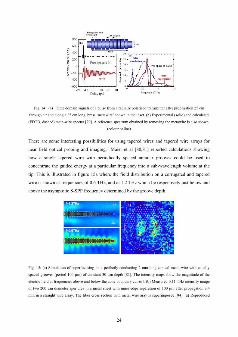
and annular groove geometries [79,80,81]. Figures 14a and 14b show time and frequency
domain experimental results for S-SPPs on a cylindrical wire with simple annular grooves
end-fire excited by quasi-radially polarised pulses [18,79]. The calculated asymptotic cut-off
for the lowest and highest order azimuthal modes are indicated by the vertical bars in figure
14b. The majority of the spectral weight is associated with higher order azimuthal modes in
both experiment and FDTD simulation for reasons not presently understood. The simulation
shows a cut-off near the lowest order, azimuthally independent mode that is not observed in
the experiment, posssibly because the simulation uses linearly polarised plane wave exitation.
24
Fig. 14 : (a) Time domain signals of a pulse from a radially polarised transmitter after propagation 25 cm
through air and along a 25 cm long, brass ‘metawire’ shown in the inset. (b) Experimental (solid) and calculated
(FDTD, dashed) meta-wire spectra [79]. A reference spectrum obtained by removing the metawire is also shown.
(colour online)
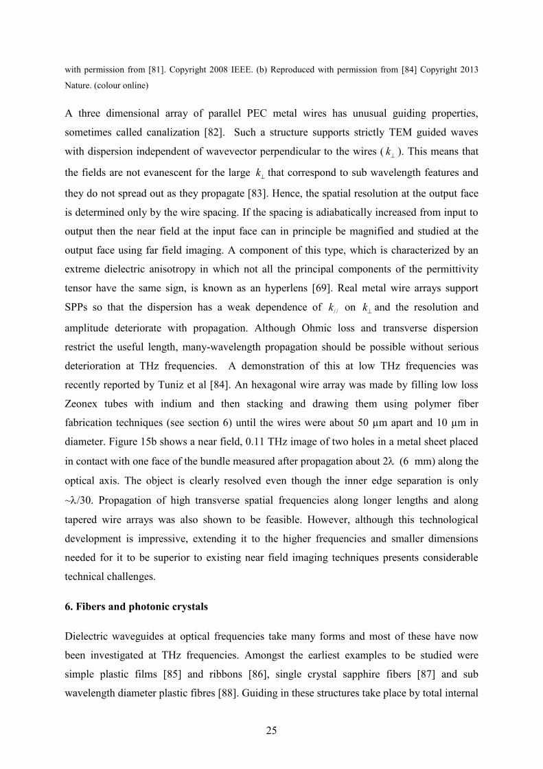
There are some interesting possibilities for using tapered wires and tapered wire arrays for
near field optical probing and imaging. Maier et al [80,81] reported calculations showing
how a single tapered wire with periodically spaced annular grooves could be used to
concentrate the guided energy at a particular frequency into a sub-wavelength volume at the
tip. This is illustrated in figure 15a where the field distribution on a corrugated and tapered
wire is shown at frequencies of 0.6 THz, and at 1.2 THz which lie respectively just below and
above the asymptotic S-SPP frequency determined by the groove depth.
Fig. 15: (a) Simulation of superfocusing on a perfectly conducting 2 mm long conical metal wire with equally
spaced grooves (period 100 µm) of constant 30 µm depth [81]. The intensity maps show the magnitude of the
electric field at frequencies above and below the zone boundary cut-off. (b) Measured 0.11 THz intensity image
of two 200 µm diameter apertures in a metal sheet with inner edge separation of 100 µm after propagation 3.4
mm in a straight wire array. The fiber cross section with metal wire aray is superimposed [84]. (a) Reproduced
25
with permission from [81]. Copyright 2008 IEEE. (b) Reproduced with permission from [84] Copyright 2013
Nature. (colour online)
A three dimensional array of parallel PEC metal wires has unusual guiding properties,
sometimes called canalization [82]. Such a structure supports strictly TEM guided waves
with dispersion independent of wavevector perpendicular to the wires ( k ). This means that
the fields are not evanescent for the large k that correspond to sub wavelength features and
they do not spread out as they propagate [83]. Hence, the spatial resolution at the output face
is determined only by the wire spacing. If the spacing is adiabatically increased from input to
output then the near field at the input face can in principle be magnified and studied at the
output face using far field imaging. A component of this type, which is characterized by an
extreme dielectric anisotropy in which not all the principal components of the permittivity
tensor have the same sign, is known as an hyperlens [69]. Real metal wire arrays support
SPPs so that the dispersion has a weak dependence of k/ / on k and the resolution and
amplitude deteriorate with propagation. Although Ohmic loss and transverse dispersion
restrict the useful length, many-wavelength propagation should be possible without serious
deterioration at THz frequencies. A demonstration of this at low THz frequencies was
recently reported by Tuniz et al [84]. An hexagonal wire array was made by filling low loss
Zeonex tubes with indium and then stacking and drawing them using polymer fiber
fabrication techniques (see section 6) until the wires were about 50 µm apart and 10 µm in
diameter. Figure 15b shows a near field, 0.11 THz image of two holes in a metal sheet placed
in contact with one face of the bundle measured after propagation about 2 mm) along the
optical axis. The object is clearly resolved even though the inner edge separation is only
~/30. Propagation of high transverse spatial frequencies along longer lengths and along
tapered wire arrays was also shown to be feasible. However, although this technological
development is impressive, extending it to the higher frequencies and smaller dimensions
needed for it to be superior to existing near field imaging techniques presents considerable
technical challenges.
6. Fibers and photonic crystals
Dielectric waveguides at optical frequencies take many forms and most of these have now
been investigated at THz frequencies. Amongst the earliest examples to be studied were
simple plastic films [85] and ribbons [86], single crystal sapphire fibers [87] and sub
wavelength diameter plastic fibres [88]. Guiding in these structures take place by total internal

26
reflection (TIR) at the core-air boundary with a significant fraction of the wave extending in
to the air. A large air fraction and thus low attenuation and dispersion can be arranged by
reducing the thickness or diameter but at the expense of poor confinement and consequent
loss due to imperfections, bends and scattering by nearby objects. As an example, Chen et al
[88] found an attenuation constant of order 0.4 dB/m in a 200 µm diameter HDPE fiber at 0.3
THz. The attenuation and dispersion strongly increase with increasing frequency due to a
diminishing air fraction.
Following this early work, attention switched to microstructured optical fibers (MOFs), also
called photonic crystal fibers (PCF). MOFs were first developed in silica for near infrared
applications and thanks to the excellent physical properties of silica, they can be produced
with a precision at the nanoscale in a wide variety of highly functional forms which have lead
to advances in nonlinear optics and the development of new optical sources and other devices
[89]. At THz frequencies, silica is very lossy but a variety of reasonably low loss polymers
amenable to fiber drawing can be substituted if only short propagation lengths are desired.
THz polymer MOFs are fabricated using a similar processes to that used for silica MOFs. In
the first manufacturing step, a many-cm-diameter version of the structure, called a preform, is
created by stacking tubes by hand, sometimes inside a jacket or sometimes the jacket is added
at a later stage. Alternatively, a preform is created by precision drilling of holes in a solid
cylinder or by extrusion. The preform is drawn down, extending its length and reducing its
diameter to ~ 5 mm or so, sometimes with pressure applied to the core and capillaries to
prevent tubes collapsing or to otherwise tailor the final internal shape. It should be noted that
MOFs of this diameter are not very flexible but that they can be bent, at least with the aid of
some heat softening. The choice of polymer is very important because dielectric loss at THz
frequencies is generally large. The lowest loss materials of choice are currently cyclic olefins,
such as those with the trade names Zeonex and Topas, which have absorption coefficents of
order 0.2 cm-1 (87 dB/m) at 1 THz [90,91]. Other choices, but with order of magnitude higher
absorption [92], are HDPE and PTFE.

27
Fig. 16: Examples of some possible fiber designs. The first row shows guides relying on TIR: (a) subwavelength
fiber, (b) suspended core, (c) low index discontinuity guide, (d) solid core fiber with low index photonic crystal
cladding (e) porous core fiber with sub-wavelength holes. White represents air and gray represents dielectric.
The second row shows air core fibers which do not guide by TIR: (f) thin wall tube guide (g,h) two additional
air core ARROW guide designs, (i) a kagome style fiber and (j) a photonic band gap fiber. The third row shows
some real polymer fibers designed for THz operation: (k) suspended core [90], (l) kagome type [108] and (m)
solid core with low index cladding. (k) reproduced with permission from [90]. Copyright 2011 Optical Society
of America. (l) reproduced with permission from [108]. Copyright 2011 Optical Society of America. (m)
reproduced from [91]. Copyright 2009 Optical Society of America
A large variety of fiber geometries have now been explored by various groups. These can be
broadly divided into three classes according to the guidance mechanism: (a) those relying on
TIR and which therefore support true guided modes, (b) those which guide by grazing
incidence reflection in hollow cores and therefore support only leaky modes and (c) those
which guide by means of a photonic bandgap. Figure 16 shows schematic examples of guides
of these different types which we now describe in more detail, starting with those based on
TIR.
In addition to the simple sub-wavelength diameter solid fiber mentioned earlier (figure 16a),
there are several other THz dielectric guide designs relying on TIR and these are shown in the
top row of figure 16. One simple variation [90] is to suspend a wavelength-scale solid core on
struts inside a jacket to allow handling with minimal effect on guidance (figures 16b and

28
16k). Another approach is to use a thick walled tube with a wavelength scale diameter hollow
core known as a low-index discontinuity guide [93] (figure 16c). Here, the bulk of the wave
resides in the core, thus reducing attenuation and dispersion, but TIR at the outer dielectric
boundary confines the guided mode.
A further variation is to take a solid core fibre and surround it by a porous, low index cladding
threaded by sub-wavelength diameter air holes (figure 16d). The guide in figure 16a can be
thought of as an extreme case of that in figure 16d. The porous cladding guide is similar to a
conventional step index fiber but with a much larger difference in effective refractive index
between core and cladding and has been intensively studied in near infrared MOFs [94].
Single mode operation is made easier by the larger step in effective index and can be ensured
by approriate choice of the ratio of hole diameter to pitch. The first example of this type of
structure at THz frequencies was described by Han et al [95]. A more refined version was
later reported by Nielsen et al [91] (figure 16m). The latter authors reported less than 10 dB/m
loss at 0.6 THz in single mode Topas fibers, which is 5 times smaller than the bulk material
loss at the same frequency. Some reduction in loss is expected because a fraction of the
guided mode resides in air although the reason why the loss was so much lower was not clear.
Fig. 17 (a),(b) Calculated guided mode structure at 1 THz for a large and small mode area fibers (LMA, SMA)
having different hole pitches. (c),(d) Time domain signals and intensity maps showing spectral amplitude versus
time after propagation along a 29 mm length of LMA and a 26 mm length of SMA fiber. The bottom panels
show the calculated GVD. The larger GVD below 0.5 THz for the SMA gives rise to larger pulse broadening
and chirp. Reproduced with permission from [91]. Copyright 2009 Optical Society of America. (colour online)

29
Varing the cladding porosity by changing the hole spacing gives control of the mode area and
waveguide dispersion, as shown in figure 17. The GVD values shown in figure 17c are
similar to those obtained in the suspended core design of Anthony et al [90] which has a
comparable mode area. At long wavelengths the behaviour of porous cladding structures
tends to that of porous fibers in which there is no distinction between core and cladding
(figure 16e) and which provide yet another TIR approach [96,97]. For the same attenuation,
porous fibres provide stronger confinement (smaller mode area) than solid core fibers [97] but
weaker confinement than low index cladding structures.
The air core fibers shown in figures 16f to 16i support only leaky core modes which couple to
transverse radiation modes via leaky modes in the cladding. Guidance relies on the high
reflectivity at an air-dielectric boundary for grazing incidence light. The incident angle range
is of order a where a is the core radius and the core diameter must be larger than 1 or 2
mm at 1 THz for reasonably high reflectivity. The simplest example of a leaky guide is the
thin wall tube (figure 16f). This was theoretically discussed as a THz guide by Miyagi and
Nishida as long ago as 1980 [98] and later explored experimentally in commercially available
PTFE tubes by Lai et al [99]. The latter authors reported an attenuation as low as 0.4 dB/m for
a 9 mm diameter, 0.5 mm wall thickness tube near 0.4 THz. The minimum attenuation is
proportional to /a3 if the walls thickness and material absorption are sufficiently large and
to 3/a4 in the opposite limit relevant to their work [100]. Scaling the result to a more practical
diameter of 2 mm thus gives a much higher attenuation of ~26 dB/m. Dielectric tube guides
are fundamentally multimode but leakage loss increases strongly with mode order so that
propagation of just the fundamental HE11 mode can be arranged by suitable choice of
diameter and length, and the dispersion is relatively low because of the large air fraction. The
guiding mechanism in this type of leaky guide is known as anti-resonant reflection optical
waveguiding (ARROW) [101] because it also depends on avoiding resonant transmission
through the core walls which can be considered as Fabry-Perot cavities. The Fabry-Perot
resonances thus define high loss bands, between which anti-resonant guiding takes place. The
mth resonant frequency is given by
fm mc
2t nclad2 ncore
2 [8]
where t is the wall thickness. To achieve a large bandwidth for transmission, thin walls are
preferable but the thickness cannot be so small that the desired frequency range is

30
significantly below f1 because guiding eventually fails with diminishing frequency as the
grazing incidence approximation breaks down and the reflectivity becomes small.
Other possible ARROW designs, which facilitate fabrication of thinner core walls whilst
maintaining fiber robustness, are shown in figures 16g and 16h. In these structures the core is
separated from the outer jacket by a single ring of struts or tubes which we call the ‘cladding’.
Interference between reflections at the inner and outer cladding boundaries leads to a
requirement that the cladding thickness is approximately equal to 0.65a for minimum leakage
[102]. Adding a second ring of tubes can reduce leakage a little more but adding even more
rings has negligible effect. The design in figure 16g is being developed for the medium wave
infrared [103] and has intrinsically higher attenuation than those based on TIR or bandgap
guiding if material loss is neglected. However, when material loss is large, such as is the case
at mid infrared and THz frequencies, then the ARROW type might be competitive. For
example, calculations for a structure similar to that in figure 16h and consisting of a ring of
twelve 1.4 mm diameter PTFE tubes with 44 µm thick walls encircling a 4.2 mm diameter
core suggest that a loss as low as 0.1 dB/m in the fundamental HE11-like mode should be
possible over a 1 THz range around 2 THz [104]. This is promisingly better than so far
obtained using dielectric coated metal tubes or TIR guiding in MOFs when scaled to similar
mode area but more work is needed on this type of guide to confirm its potential. There are
also some subtleties which might be exploited to increase performance further. For example,
the role of curvature of the core walls appears to be important; folding of the core boundary
compresses the mode area and reduces , thus weakening core-cladding coupling [105].
The air core structure in figure 16g was originally introduced in the near infrared as a simpler
version of the kagome (‘basket weave’) fibre [106] sketched in figure 16i, where all but a
single ring of tubes around the core are removed. The first silica kagome fiber [106] had a
cladding lattice formed by a large number of rings of thin walled hexagonal tubes. The precise
cladding structure and periodicity are effectively unrelated to the guiding mechanism in the
sense that there is no photonic bandgap at the guiding frequencies. Guidance is dependent on
the ARROW mechanism, with coupling of the core mode to modes in the cladding inhibited
by a large phase mismatch and a low density of cladding states [106]. Experiements on THz
versions of the kagome fiber with the hexagonal tubes replaced by circular ones were reported
by Lu et al [107] and Anthony et al [108] ( Figure 16l). In Lu et al’s structure, which had a 5
mm diameter core, the attenuation was ~ 1 dB/m at 0.5 THz whilst in Anthony et al’s work,

31
the core diameter was 2.2 mm and the measured and calculated attenuation was much higher
with a value of ~ 80 dB/m near 1 THz. It is important to understand whether the large
difference simply reflect the different structural parameters such as core diameter and tube
wall thickness and therefore to what extent low attenuation can be engineered.
Except near wall resonances (equation 8), the waveguide dispersion of the kagome fiber
[109] and other ARROW type structures can be described by a similar expression to that for a
thick walled air filled tube given by [110]
2
1
1
2
u11
2a
2
. [9]
Equation 9 looks like the ka>>1 limit of equation 1, except one has to be aware that leaky
modes have no cut-offs. The GVD in hollow dielectric MOFs is therefore similar to that of
dielectric lined metal tubes of the same diameter. For a=1 mm equation 9 predicts a GVD of -
0.07 ps/THz/cm which is consistent with measurements by Anthony et al [108] and similar to
that calculated for the solid core MOF in figure 17 [92].
Finally, to end this section, we point out that true guided modes can be engineered in hollow
core MOFs by constructing the cladding as a Bragg mirror of alternating high and low index
regions to form what are known as bandgap guiding fibers (figure 16j). Low loss photonic
bandgap guiding is extremely effective in silica fibers made for the near infrared but at THz
frequencies the bandwidth is limited compared with some other designs and material loss is
relatively large. For example, Ponseca et al [111] constructed a 5 ring bandgap guiding MOF
in PMMA and obtained a minimum loss of ~ 90 dB/m for a core diameter of 0.67 mm which
is rather close to the expected material loss, perhaps suggesting that the bandgap guidance is
weak with so few rings.
7. Conclusions and outlook
There is now a large body of work exploring waveguide concepts at THz frequencies with
potential applications ranging from power delivery to sensing and near field imaging. Some
of these already exhibit acceptable enough properties for immediate exploitation. Ones that
stands out in this respect are the very low loss metal-dielectric lined tube which is being
actively explored for delivery of narrow band QCL radiation and the latest generation of
planar transmission lines which have bandwidths and frequency selectivity suitable for
32
biosensing. Metamaterial concepts might also prove useful in the latter application. Polymer
microstructured fibers have similar potential to the dielectric lined tube. In particular, the
solid core fiber with porous cladding offers single mode operation with small mode size
whilst the large mode area, hollow core fiber should in principle be capable of competitively
low loss.
Thinking further into the future, a technology that it would be useful to develop is that needed
to construct high index contrast, multilayer THz mirrors with high reflectivity for all incident
angles and polarizations [112]. Such mirrors could be used for the construction of omniguides
[113] which could have advantages over the guides reviewed above in narrowband
applications. From a more fundamental perspective, it is possible that further development of
guiding concepts such as adiabatic tapering and canalization, together with improvements in
THz source intensities and detector sensitivities, might one day allow the efficient
concentration and detection of THz radiation on sub-micron length scales and thus open up a
new era of nanoscale terahertz science. Such developments might well be facilitated by new
3D metamaterials such as the recently reported polymer-metal composite fibers with
plasmonic and magnetic response [114,115] and graphene-dielectric stacks [116]. The rather
extreme bandwidth and low dispersion required for guidance of the broadband THz radiation
used in time domain THz spectroscopy remains elusive in all but the parallel plate waveguide
and its variants, but new concepts or technologies might appear that could address this issue
or at least render it less important. For example, the development of widely tunable cascade or
other types of THz laser could displace the time domain technique in some applications.
Whatever the future holds, it is clear that the subject of terahertz guiding will continue to
throw up challenges and solutions and reveal new insights into our ability to manipulate light.
Acknowledgements
It is a pleasure to acknowledge fruitful collaborations on THz waveguiding with Chris
Williams, Antonio Fernandez-Dominguez, Mukul Misra, Yi Pan, Stefan Maier, Francisco
Garcia-Vidal and Luis Martin-Moreno. The author would like to acknowledge financial
support by the Engineering and Physical Science Research Council (Grant number
EPJ007595/1/] during the writing of this review.

33
References
[1] M. Tonouchi, ‘Cutting edge terahertz technology’, Nature Photonics 1, 97 (2007)
[2] D. Grischkowsky, S.Keiding. M. van Exter and Ch. Fattinger, ‘Far-infrared time-domain
spectroscopy with terahertz beams of dielectrics and semiconductors’, J. Opt. Soc. Am. B 7,
2006 (1990)
[3] J. Shah, ‘Ultrafast spectroscopy of semiconductors and semiconductor nanostructures’,
Springer, New Yoprk (1996)
[4] R. M. Woodward, V. P. Wallace, D. D. Arnone, E. H. Linfield and M. Pepper,
‘Terahertz pulsed imaging of skin cancer in the time and frequency domain‘, J. Biol. Phys.
29, 257 (2003)
[5] C. J. Strachan, P. F. Taday, D.A. Newnham, K. C. Gordon, J. A. Zeitler, M.Pepper and T.
Rades, ‘Using terahertz pulsed spectroscopy to quantify pharmaceutical polymorphism and
crystallinity’, J. Pharmaceutical Sciences 94, 837 (2005)
[6] R. Piesiewicz, T. Kleine-Ostmann, N. Krumbholz, D. Mittleman, M. Koch, J. Schoebel
and T. Koerner, ‘Short-range ultra-broadband terahertz communications: concepts and
perspectives’, IEEE Antennas Propag. Mag. 49, 24-39 (2007).
[7] K. Yamamoto, M. Yamaguchi, F. Miyamaru, M. Tani, M. Hangyo, T. Ikeda, A.
Matsushita, K. Koide, M. Tatsuno and Y. Minami, ‘Non-invasive inspection of C-4 explosive
in mails by terahertz time-domain spectroscopy’, Japanese Journal of Applied Physics Part 2 -
Letters 43, L414 (2004).
[8] M. Nagel, P. Haring Bolivar, M. Brucherseifer and H. Kurz, ‘Integrated THz technology
for label-free genetic diagnostics‘, Appl. Phys. Letts. 80, 154 (2002).
[9] X.-C. Zhang and J. Xu, ‘Introduction to THz wave photonics’, Springer, New York (2010)
[10] R. Köhler, A. Tredicucci, F. Beltram, H. E. Beere, E. H. Linfield, A. G. Davies, D. A.
Ritchie, R. C. Iotti and F. Rossi, ‘Terahertz semiconductor-hetersostructure laser’, Nature
417, 156 (2002)

34
[11] C. Sirtori, S. Barbieri and R. Colombelli, ‘Wave engineering with THz quantum cascade
lasers’, Nature Photonics 7, 691 (2013)
[12] H. Ito, F. Nakajima, T. Furuta and T. Ishibashi, ‘Continuous THz-wave generation using
antenna-integrated uni-travelling-carrier photodiodes’, Semiconductor Science and
Technology 20, S191 (2005)
[13] D. Molter, A. Wagner, S. Weber, J. Jonuscheit and R. Beigang, ‘Combless broadband
terahertz generation with conventional laser diodes’, Optics Express 19, 5290 (2011)
[14] Z. Mihoubi, K. G. Wilcox, S. Elsmere, A. Quarterman, R. Rungsawang, I. Farrer, H. E.
Beere, D. A. Ritchie, A. Tropper and V. Apostolopoulos, ‘All-semiconductor room=-
temperature terahertz time domain spectrometer’, Optics Lett. 33, 2125 (2008)
[15] H. Dai, J. Zhang, W. Zhang and D. Grischkowsky, ‘Terahertz time-domain spectroscopy
characterization of the far-infrared absorption and index of refraction of high-resistivity float-
zone silicon’, JOSA B, 21, 1379 (2004)
[16] O. Mitrofanov, T. Tan, P. R. Mark, B. Bowden and J. A. Harrington, ‘Waveguide mode
imaging and dispersion analysis with terahertz near-field microscopy’, Appl. Phys. Lett. 94,
171104 (2009)
[17] M. Wächter, M. Nagel and H. Kurz, “Metallic slit waveguide for dispersion-free low-loss
terahertz signal transmission”, Appl. Phys. Lett. 90, 061111 (2007)
[18] T.-I. Jeon, J. Zhang and D. Grischkowsky, ‘THz Sommerfeld wave propagation on a
single metal wire’, Appl. Phys. Lett. 86, 161904 (2005)
[19] J. R. Knab, A. J. L. Adam, M. Nagel, E. Shaner, M. A. Seo, D. S. Kim and P. C. M.
Planken, ‘Terahertz near-field vectorial imaging of subwavelength apertures and aperture
arrays’, Optics Express 17, 15072 (2009)
[20] M. Wächter, M. Nagel and H. Kurz, ‘Tapered photoconductive terahertz field probe tip
with subwavelength spatial resolution’, Appl. Phys. Lett. 95, 041112 (2009)
[21] M. Misra, Y. Pan, C. R. Williams, S. A. Maier and S. R. Andrews, ’Characterization of a
hollow core fiber-coupled near field terahertz probe’, J. Appl. Phys. 113, 193104 (2013)

35
[22] V. Astley, R. Mendis and D. M. Mittleman, ‘Characterization of terahertz field
confinement at the end of a tapered metal wire waveguide’, Appl. Phys. Lett. 95, 031104
(2009)
[23] A. Taflove, ‘Computational Electrodynamics: the finite difference time domain method’,
2nd edition, (Norwood, MA, Artech House, 2000)
[24] D. R. Grishkowsky, ‘Optoelectronic characterization of transmission lines and
waveguides by terahertz time-domain spectroscopy‘, IEEE J, Sel. Topics in Quant. Electron.
6, 1122 (2000)
[25] S. Atakaramians, S. Afshar V., T. M. Monro and D. Abbott, ‘Terahertz dielectric
waveguides’, Advances in Optics and Photonics 5, 169 (2013)
[26] R. W. McGowan , G. Gallot and D. Grischkowsky, ‘Propagation of ultra-wide band,
short pulses of THz radiation through sub-mm diameter circular waveguides’, Opt. Lett. 24,
1431-1433 (1999)
[27] G. Gallot, S. P. Jamison, R. W. McGowan and D. Grischkowsky, ‘Terahertz
waveguides’, J. Opt. Soc. Am. B 17, 851-863 (2000)
[28] N. Marcuwitz, ‘Waveguide handbook’. Peter Peregrinus, London (1993)
[29] Y. Kato and M. Miyagi:, ‘Modes and Attenuation Constants in Circular Hollow
Waveguides with Small Core Diameters for the Infrared’, IEEE Trans, MTT 40, 679 (1992)
[30] E. A. J. Marcatili and R. A. Schmeltzer, ‘Hollow metallic and dielectric waveguides for
long distance optical transmission and lasers’, Bell System Technical Journal 43, 1783-1809
(1964).
[31] C. Dragone, ‘Attenuation and radiation characteristics of the HE11-mode’, IEEE Trans,
on Microwave Theory and Techniques, 28, 704 (1980)
[32] E. A. Nanni, D. K. Jawla, M. A. Shapiro, P. P. Woskov and R. J. Temkin, ‘Low-loss
Transmission Lines for High-Power Terahertz Radiation’, J. Int. Millim. Terahertz Waves,
33, 695 (2012)

36
[33] E. de Rijk, A. Macor, J-Ph. Hogge, S. Alberti and J-Ph. Ansermet ‘Note: Stacked rings
for teraahertz wave-guiding’, Rev. Sci. Instrum., 82, 066102 (2011)
[34] B. Bowden, J. A. Harrington and O. Mitrofanov, ‘Silver/polystyrene-coated hollow glass
waveguides for the transmission of terahertz radiation’, Optics Letts. 32, 2945 (2007)
[35] J. R. Birch, J. D. Dromey and J. Lesurf, ‘The optical constants of some common low-loss
polymers between 4 and 40 cm-1’, Infrared Phys. 21, 225 (1981)
[36] M. Miyagi and S. Kawaklami, ‘Design Theory of Dielectric-Coated Circular Metallic
Waveguides for Infrared Transmission’, J. Lightwave Technol. 2, 116 (1984)
[37] M. A. Ordal, R. J. Bell, R. W. Alexander, L. L. Long and M. R. Querry, ‘Optical
properties of fourteen metals in the infrared and far infrared:Al, Co, Cu, Au, Fe, Pb, Mo, Ni,
Pd, Pt, Ag, Ti, V and W’, Applied Optics 24, 4493 (1985)
[38] J. A. Harrington, R. George, P. Pedersen and E. Mueller, ‘Hollow polycarbonate
waveguides with inner Cu coatings for delivery of terahertz radiation’, Opt. Express 12, 5263
(2004)
[39] Y-I Jeon and D. Grischkowsky, Direct optoelectronic generation and detection of sub-ps-
electrical pulses on sub-mm-coaxial transmission lines’, Appl. Phys. Lett. 85, 6092 (2004)
[40] R. Mendis and D. Grischkowsky, ‘Undistorted guided-wave propagation of
subpicosecond terahertz pulses’, Optics Letts., 26, 846 (2001)
[41] N. Laman and D. Grischkowsky, ‘Terahertz conductivity of thin metal films‘, Appl.
Phys. Lett. 93, 051105 (2008)
[42] J. Zhang and D. Grischkowsky, Waveguide terahertz time-domain spectroscopy of
nanometer water layers’, Optics Lett. 29, 1617 (2004)
[43] R. Mendis and D. Grischkowsky, ‘THz interconnect with low-loss and low-group
velocity dispersion’, IEEE Microwave and Wireless Components Lett. 11, 444 (2001)
[44] S. Atakaramians, S. Afshar V, M. Nagel, H. K. Ramussen, O. Bang, T. Monro and D.
Abbott, ‘Direct probing of evanescent field for characterization of porous terahertz fibers’,
Appl. Phys. Lett. 98, 121104 (2011)

37
[45] M. Nagel, M. Först and H. Kurz, ‘THz biosensing devices: fundamentals and
technology’, J. Phys. Condens. Matter 18, S601-S618 (2006)
[46] P. A.George, C. Manolatou, F. Rana, A. L. Bingham and D. R. Grischkowsky ‘Integrated
waveguide-coupled terahertz microcavity resonators’, Appl. Phys. Lett. 91, 191122 (2007)
[47] A. L. Bingham and D. Grischkowsky, ‘Terahertz two-dimensional high-Q photonic
crystal waveguide cavities’, Optics lett. 33, 348 (2008)
[48] H. Zhan, R. Mendis and D. M. Mittleman, ‘Superfocusing terahertz waves below λ/250
using plasmonic parallel-plate waveguides’, Optics Express 18 ,9643–9650 (2010).
[49] A. Rusina, M. Durach, K. A. Nelson and M. Durach, M. I. Stockman,
‘Nanoconcentration of terahertz radiation in plasmonic waveguides’, Optics Express 16,
18576-18589 (2008)
[50] R. Mendis and D. M. Mittleman, ‘Comparison of the lowest-order transverse-electric
(TE1) and tranverse-magnetic (TEM) modes of the parallel-plate waveguide for terahertz
pulse applications’, Optics Express 17, 14839 (2009)
[51] R. Mendis and D. M. Mittleman, ‘Multifaceted terahertz applications of parallel-plate
waveguide TE1 mode’, Electronics Lett. Special Supplement: Terahertz Technology, S40
(2010)
[52] T. Ohkubo, M. Onuma, J. Kitaghawa and Y. Kadoya, ‘Micro-strip-line-based sensing
chips for charcterization of polar liquids in terahertz regime’, Appl. Phys. Lett. 88, 212511
(2006)
[53] M. Nagel, P. Haring Bolivar, M. Brucherseifer and H. Kurz ‘Integrated THz technology
for label-free genetic diagnostics’, Appl. Phys. Lett. 80, 154-156 (2002)
[54] L. Cao, A-S Grimault, N. Zerounin and F. Aniel, ‘Design and VNA-measurement of
coplanar waveguide (CPW) on benzocyclobutene (BCB) at THz frequencies‘, Infared Physics
and Tech. 63, 157 (2014)
[55] R. W. McGowan, D. Grischkowsky and J. A. Misewich, ‘Demonstrated low radiative
loss of a quadrupole ultrashort electrical pulse propagated on a three strip coplanr
transmission line’, Appl. Phys. Lett. 71, 2842 (1997)

38
[56] Y. Kadoya, M. Onuma, S. Yanagi, T. Ohkubo, N. Sato and J. Kitagawa, ‘THz wave
propagation on strip lines: devices, properties and applications’, Radioengineering 17, 48
(2008)
[57] F. Schneider and W. Heinrich, ‘Thin-film microstrip lines and coplanar waveguides on
semiconductor substrates for sub-mm wave frequencies’, Frequenz 59, 5 (2006)
[58] M. Y. Frankel, S. Gupta, J. A. Valdmanis and G. A. Morou, ‘Terahertz attenuation and
dispersion characteristics of coplanar transmission lines’, IEEE Trans. MTT 39, 910 (1991)
[59] D. Grischkowsky, I. N. Duling, J. C. Chen and C.-C. Chi, ‘Electromagnetic shock waves
from transmission lines’, Phys. Rev. Lett. 59, 1663 (1987)
[60] H. -M. Heiliger, M. Nagel, H. G. Roskos, H. Kurz, F. Schneider, W. Heinrich, R. Hey
and K. Ploog, ‘Low-dispersion thin-film microstrip lines with cyclotene (benzocyclobutene)
as dielectric medium’, Appl. Phys. Lett.70, 2233 (1997)
[61] J. Cunningham, C. Wood, A. G. Davies, C. K. Tiang, P. Tosch, D. A. Evans, E. H.
Linfield, I. C. Hunter and M. Missous, ‘Multiple-frequency terahertz pulsed sensing of
dielectric films’, Appl. Phys. Lett. 88, 071112 (2006)
[62] L. Dazhang, J. Cunningham, M. B. Byrne, S. Khanna, C. D. Wood, A. D. Burnett, S. M.
Ershad, E. H. Linfield and A. G. Davies, ‘On-chip terahertz Goubau-line waveguides with
integrated photoconductive emitters and mode-discriminating detectors’, Appl. Phys. Lett. 95,
092903 (2009)
[63] S. A. Maier, ‘Plasmonics-Fundamentals and Applications’, Springer, New York (2007)
[64] J. Saxler, J. Gomez-Rivas, C. Janke, H. P. Pellemans, P. Haring Bolivar and H. Kurz,
’Time-domain measurements of surface plasmon polaritons in the terahertz frequency range’,
Phys. Rev. B 69, 155427 (2004).
[65] T.–I. Jeon and D. Grischkowsky, ‘THz Zenneck surface wave propagation on a metal
sheet’, Appl. Phys. Lett. 88, 061113 (2006)
[66] G. Goubau, ‘Surface Waves and Their Application to Transmission Lines’, J. Appl.
Phys. 21, 1119 (1950)

39
[67] D. L. Mills and A. A. Maradudin, ‘Surface corrugation and surface-polariton binding in
the infrared frequency range’, Phys. Rev. B 39, 1569 (1989)
[68] J. B. Pendry, L. Martín-Moreno and F. J. García-Vidal, ‘Mimicking surface plasmons
with structured surfaces’, Science 305, 847–848 (2004).
[69] Z. Liu, H. Lee, Y. Xiong, C. Sun and X. Zhang, ‘Far-field optical hyperlens magnifying
sub-diffraction-limited objects’, Science 315, 1686 (2007)
[70] D. Shurig, J. J. Mock, B. J. Justice, S. A. Cummer, J. B. Pendry, A. F. Starr and D. R.
Smith, ‘Metamaterial electromagnetic cloak at microwave frequencies’, Science 314, 977
(2006)
[71] R. Ulrich and M. Tacke, ‘Submillimeter waveguiding on periodic metal structure’, Appl.
Phys. Lett. 22, 251 (1973)
[72] C. R. Williams, S. R. Andrews , S. A. Maier, A. I. Fernandez-Dominguez, L. Martin-
Moreno and F. J. Garcia-Vidal, 'Highly confined guiding of terahertz surface plasmon
polaritons on structured metal surfaces', Nature Photonics 2, 175-179 (2008)
[73] C. R. Williams, M. Misra, S. R. Andrews, S. Carretero Palacios, L. Martin-Moreno, F. J.
Garcia Vidal and S. A. Maier, ‘Dual band THz waveguiding on a planar metal surface
patterned with annular grooves’, Appl. Phys. Lett. 96, 11101 (2010)
[74] S. A. Maier and S. R. Andrews, ‘Terahertz pulse propagation using plasmon-polariton-
like surface modes on structured conductive surfaces’, Appl. Phys. Lett. 88, 251120 (2006)
[75] W. Zhu, A. Agrawal and A. Nahata, ‘Planar plasmonic terahertz guided-wave devices’,
Optics Express 16, 6216 (2008)
[76] K. Wang and D. M. Mittleman, ‘Metal wires for terahertz wave guiding’, Nature 432,
376-379 (2004)
[77] N. C. J. van der Valk and P. C. M. Planken, ‘Effect of a dielectric coating on terahertz
surface plasmon polaritons on metal wires’, Appl. Phys. Lett. 87, 071106 (2005) .
40
[78] A.I. Fernandez-Dominguez, C. R. Williams, F. J. Garcia-Vidal, L. Martin-Moreno, S. R.
Andrews and S. A. Maier,' Terahertz surface plasmon polaritons on a helically grooved wire,
Appl. Phys. Lett. 93, 141109 (2008)
[79] C. R. Williams, ‘Terahertz waveguiding on metamaterials’, PhD thesis, University of
Bath (2009)
[80] S. A. Maier, S. R. Andrews, L. Martin-Moreno and F. J. Garcia-Vidal, ‘Terahertz
surface plasmon-polariton propagation and focusing on periodically corrugated metal wires’,
Phys. Rev. Lett. 97, 176805 (2006)
[81] A. Fernandez-Dominguez, L. Martin-Moreno, F. J. Garcia-Vidal, S. R. Andrews and S.
A. Maier, ‘Spoof surface plasmon polariton modes propagating along periodically corrugated
wires’, IEEE Sel. Topics Quant. Electron. 14, 1515 (2008)
[82] P.A. Belov, C. R. Simovski and P. Ikonen, ‘Canalization of subwavelength images by
electromagnetic crystals‘, Phys. Rev. B 71, 193105 (2005)
[83] G. Shvets, S. Trenafilov, J. B. Pendry and A. Sarychev, ‘Guiding, focusing, and sensing
on the subwavelength scale uisng metallic wire arrays’, Phys. Rev. Lett. 99, 053903 (2007)
[84] A. Tuniz, K. J. Kaltenecker, B. M. Fischer, M. Walther, S. C. Fleming, A. Argyros and
B. T. Kuhlmey, ‘Metamaterial fibres for subdiffraction imaging and focusing at terahrtz
frequencies over optically long distances’, Nature Communications 4, 2706 (2013)
[85] M. Tacke and R. Ulrich, ‘Submillimeter wave-guiding on thin dielectric films’, Optics
Communications 8, 234-238 (1973)
[86] R. Mendis and D. Grischkowsky, ‘Plastic ribbon THz waveguides’, J. Appl. Phys. 88,
4449-4451 (2000).
[87] S. P. Jamison, R. W. McGowan and D.Grischkowsky, ‘Single-mode waveguide
propagation and reshaping of sub-ps terahertz pulses in sapphire fibers’, Appl. Phys. Lett. 76,
1987 (2000)
[88] L. J. Chen, H. W. Chen, T. F. Kao, J. Y. Lu, and C. K. Sun, ‘Low-loss subwavelength
plastic fiber for terahertz waveguiding’, Optics Letters 31, 308-310 (2006)

41
[89] P. S. J. Russell, ‘Photonic-crystal fibers’, Journal of Lightwave Technology 24, 4729-
4749 (2006)
[90] J. Anthony, R. Leonhardt, A. Argyros and M. C. J. Large, ‘Characterization of a
microstructured Zeonex terahertz fiber’, JOSA B 28, 1013 (2011)
[91] K. Nielsen, H. K. Rasmussen, A. J. L. Adam, P. C. M. Planken, O. Bang and P. Uhd
Jepsen, ‘Bendable, low-loss Topas fibers for the terahertz frequency range’, Optics Express
17, 8592 (2009)
[92] Y-S. Jin, G-J Kim and S-G Jeon, ‘Terahertz dielectric properties of polymers’, J. Korean
Phys. Soc. 49, 513 (2006)
[93] M. Nagel, A. Marchewka and H. Kurz, ‘Low index discontinuity terahertz waveguides’,
Optics Express 14, 9944-9954
[94] T. A. Birks, J. C. Knight and P. St. J. Russell, ‘Endlessly single-mode photonic crystal
fiber’, Opt. Lett. 22, 961 (1997)
[95] H. Han, H. Park and J. Kim, ‘Terahertz pulse propagation in a plastic photonic crystal
fiber’, Appl. Phys. Lett. 80, 2634 (2002)
[96] A. Hassani, A. Dupuis and M. Skorobogatiy, ‘Low loss porous terahertz fibers
containing multiple subwavelenmgth holes’, Appl. Phys. Lett. 92, 071101 (2008)
[97] S. Atakaramians, S. Afshar V, B. M. Fischer, D. Abbott and T. M. Monro, ‘Porous
fibers: a novel approach to low loss THz waveguides’, Opt. Express 16, 8845 (2008)
[98] M. Miyagi and S. Nishida, ‘A proposal of low-loss leaky waveguide for submillimeter
waves transmission’, IEEE Trans. MTT 28, 398 (1980)
[99] C.-H. Lai, Y.-C. Hsueh, H.-W. Chen, Y.-J. Huang, H.-C. Chang, and C.-K. Sun, ‘Low-
index terahertz pipe waveguides’,Optics Letters 34, 3457-3459 (2009)
[100] M. Miyagi, ‘Bending losses in hollow and dielectric tube leaky waveguides’, Applied
Optics 20, 1221 (1981)
[101] M. A. Duguay, Y. Kokubun, T. L. Koch and L. Pfeiffer, ‘Antiresonant reflecting optical
waveguides in SiO2-Si multilayer structures’, Appl. Phys. Lett. 49, 13 (1986)

42
[102] F. Poletti, J. R. Hayes, and D. Richardson, ‘Optimising the Performances of Hollow
Antiresonant Fibres’, in OSA Technical Digest (CD) (Optical Society of America, 2011)
[103] F. Yu and J. C. Knight, ‘Spectral attenuation limits of silica hollow core negative
curvature fiber’, Opt. Express 21, 21466 (2013)
[104] L. Vincetti, ‘Numerical analysis of plastic hollow core microstructured fiber for
terahertz applications’, Optical Fiber Tech., 15, 398 (2009)
[105] A. N. Kolyadin, A. F. Kosolapov, A. D. Pryamikov, A. S. Biriukov, V. G. Plotnichenko
and E. M. Dianov, ‘Light transmission in negative curvature hollow core fiber in extremely
high material loss region’, Optics Express 21, 9514 (2013)
[106] F. Couny, F. Benabid, P. J. Roberts, P. S. Light and M. G. Raymer, ‘Generation and
photonic guidance in of multi-octave optical-frequency combs’, Science 318, 1118 (2007)
[107] J.-Y. Lu, C.-P. Yu, H.-C. Chang, H.-W. Chen, Y.-T. Li, C.-L. Pan, and C.-K. Sun,
‘Terahertz air-core microstructure fiber’, Applied Physics Letters 92, 064105 (2008).
[108] J. Anthony, R. Leonhardt, S. G. Leon-Saval and A. Argyros, ‘THz propagation in
kagome hollow-core microstructured fibers’, Optics Express 19, 18470 (2011)
[109] S-J. Im, A. Husakou and J. Herrmann, ‘Guiding properties and dispersion control of
kagome lattice hollow-core photonic crystal fibers’, Opt. Express 17, 13050 (2009)
[110] E. A. J. Marcatili and R. A. Scmeltzer, ‘Hollow metallic and Dielectric Waveguides for
Long Distance Optical Transmission and Lasers’, Bell Syst. Tech. J. 43, 1783-1809 (1964)
[111] C. S. Ponseca, Jr, R. Pobre, E. Estacio, N. Sarukura, A. Argros, M. C. J. Large and M.
A. van Eijkelenborg, ‘Transmission of terahertz radiation using a microstructured polymer
optical fiber’, Optics Lett. 33, 902 (2008)
[112] N. Krumbholz, K. Gerlach, M. Koch, R. Piesiewicz, T. Kürner and D. Mittleman,
‘Omnidirectional terahertz mirrors: a key element for future terahertz communication
systems’, Appl. Phys. Lett. 88, 202905 (2006)
[113] Y. Fink, J. N. Winn, S. Fan, C. Chen, J. Michael, J. Joannopoulos and E. Thomas, ‘A
dielectric omnidirectional reflector’, Science 282, 1679-1682 (1998)

43
[114] A. Tuniz, B. T. Kuhlmey, R. Lwin, A. Wang, J. Anthony, R. Leonhardt and S. C.
Fleming, ‘Drawn metamaterials with plasmonic response at terahertz frequencies’, Appl.
Phys. Lett. 96, 191101 (2010)
[115] A. Tuniz, R. Lwin, A. Argyros, S. C. Fleming, E. M. Pogson, E. Constable, R. A. Lewis
and B. T. Kuhlmey, ‘Stacked-and-drawn metamaterials with magnetic resonances in the
terahertz range’, Opt. Express 19, 16480 (2011)
[116] I. V. Iorsh, I. S. Mukhin, I. V. Shadrirov, P. A. Belov, and Y. S. Kivshar, ‘Hyperbolic
metamaterials based on multilayer graphene structures’, Phys. Rev. B 87, 075416 (2013)