microstructure versus flaw: mechanisms of failure and strength in nanostructures
TRANSCRIPT

Microstructure versus Flaw: Mechanisms of Failure and Strength inNanostructuresX. Wendy Gu,† Zhaoxuan Wu,§ Yong-Wei Zhang,§ David J. Srolovitz,∥ and Julia R. Greer*,‡
†Division of Chemistry and Chemical Engineering, and ‡Division of Engineering and Applied Science, California Institute ofTechnology, 1200 E. California Blvd., Pasadena, California 91125, United States§Institute of High Performance Computing, 1 Fusionopolis Way, #16-16 Connexis, Singapore 138632, Singapore∥Departments of Materials Science and Engineering & Mechanical Engineering and Applied Mechanics, University of Pennsylvania,Philadelphia, Pennsylvania 19104, United States
*S Supporting Information
ABSTRACT: Understanding failure in nanomaterials is critical for the design ofreliable structural materials and small-scale devices with nanoscale components.No consensus exists on the effect of flaws on fracture at the nanoscale, butproposed theories include nanoscale flaw tolerance and maintaining macroscopicfracture relationships at the nanoscale with scarce experimental support. Weexplore fracture in nanomaterials using nanocrystalline Pt nanocylinders withprefabricated surface notches created using a “paused” electroplating method. Insitu scanning electron microscopy (SEM) tension tests demonstrate that themajority of these samples failed at the notches, but that tensile failure strength isindependent of whether failure occurred at or away from the flaw. Moleculardynamics simulations verify these findings and show that local plasticity is able toreduce stress concentration ahead of the notch to levels comparable with thestrengths of microstructural features (e.g., grain boundaries). Thus, failure occursat the stress concentration with the highest local stress whether this is at the notch or a microstructural feature.
KEYWORDS: Size effect, nanocrystalline, mechanical properties, fracture, molecular dynamics
Hard biomaterials such as shell, bone, and exoskeletonshave an exceedingly high strength and fracture toughness
that are on par with the best manmade structural materials.1,2
These biomaterials have a unifying feature; their internalstructures are hierarchically arranged, with distinct features onlength scales extending from the nano to the macro.Nanofabrication techniques have advanced to the point whereit is now possible to emulate these hierarchical structures, forexample, using ultrahigh strength nanoscale building blocksmade of carbon and inorganic nanotubes (1D) and platelets(2D), and metals with nanoscale interfaces (3D) as the load-bearing components.3−8 The high intrinsic strength of thesenanomaterials is often difficult to maintain in large-scalecomposites because a macroscopic ensemble of these structuresroutinely contain structural and/or chemical features withinindividual constituents or at the interfaces, which are sources offailure initiation.9,10 Classical fracture mechanics dictates thatsusceptibility to fracture depends on sample and/or externalflaw length scales. This implies that different behavior mayoccur at small sample sizes and that new fracture relations maybe necessary to describe the failure of nanoscale materials.11,12
Several theoretical and computational studies have beenperformed on fracture in preflawed nanoscale samples, oftenleading to conflicting interpretations. In the theoretical work ofGao et al., scaling arguments based on linear elastic fracturemechanics (LEFM) were used to define a critical length, 0.2−
400 nm for typical brittle materials, below which the strength ofa hard platelet becomes comparable to the theoretical strengthof the material regardless of the presence of structural flaws.13
These results were also supported by atomistic simulations onsimilar preflawed structures.14 This nanoscale flaw tolerance, orflaw insensitivity, has been proposed as an explanation for theextraordinary toughness found in experiments on nano-structured biomaterials like nacre and spider silk13,15 and inatomistic simulations of nanocrystalline aluminum thin filmsand polycrystalline graphene sheets, which showed failureoccurring away from the prefabricated hole.16,17 Other studiesreported a strong dependence of failure on the presence offlawsfor example, in graphene and carbon nanotubes, whereintentionally introduced holes led to strengths that are wellbelow theoretical predictions, but in good agreement withpredictions based upon classical fracture mechanics.18 Evenvery small holes in carbon nanotube sidewalls consisting of 1−6missing atoms were shown to reduce the nanotube strength by26−33%.19Few well-controlled experimental fracture tests have been
attempted at the nanoscale. An in situ transmission electron
Received: September 16, 2013Revised: October 17, 2013Published: October 29, 2013
Letter
pubs.acs.org/NanoLett
© 2013 American Chemical Society 5703 dx.doi.org/10.1021/nl403453h | Nano Lett. 2013, 13, 5703−5709
microscopy (TEM) study of tensile-loaded nanocrystallinealuminum thin films, which contained focus ion beam (FIB)milled edge notches with a radius of ∼50 nm, showed thatfailure occurred far from the notch.20 In other studies,traditional fracture testing methodologies were extended tomicron-scale using FIB milled cantilever coupons (1−10 μm insize) to investigate failure in single and bicrystalline metals andalloys.21−23 Results demonstrate that these micron-sized metalsfractured as predicted by LEFM, with fracture strength andlocation controlled by the FIB-milled structural flaw.These studies prompt several important questions about
fracture at the nanoscale, including (1) does fracture strengthdepend on the presence of flaws and on sample/flaw geometry?and (2) can the initiation point of the crack that leads to failurebe predicted based upon the location of the flaw? We addressthese questions by conducting tensile fracture experiments andmolecular dynamics (MD) simulations on similar nanosizedsamples with introduced surface flaws of known geometries. Inthis work, the term “flaw” refers to the external notches only.Nanocrystalline Pt, referred to as nc-Pt hereafter, nanocylinderswith surface notches were fabricated through pulsed electro-plating into poly(methyl methacrylate) (PMMA) templates anddo not suffer from FIB-induced damage common to manynanomechanical experiments. Typical Pt samples were ∼120nm in diameter with an ∼6 nm grain size. Tensile experimentson unnotched nc-Pt nanocylinders revealed brittle failure,rendering this to be an appropriate material model system fortesting fracture mechanics theories that assume limitedplasticity. Sizes of surface notches in these nanostructureswere of the same order of magnitude as internal microstructuralfeatures, that is, grain size. We examine the competitionbetween such prefabricated flaws and intrinsic microstructuralfeatures as preferred sites for crack initiation and discuss thesefindings using concepts from LEFM and atomistic simulations.Nanocrystalline platinum cylinders with diameters of 117 ± 3
nm and lengths of 750 ± 40 nm were fabricated with one ormore surface flaws using a template-assisted electroplatingmethod described in Gu et al.24 Cylinders were electroplatedinto nanoscale pores in PMMA on top of a conductive goldsurface. The PMMA layer was subsequently removed to leavefreestanding cylinders. Nanoscale structural flaws were formedon the outer surface of the cylinder by ramping voltage from 0to 0.6 V at 85 mV/s, pausing the electroplating process for
approximately five minutes, replacing the electroplating bath,and then applying two more pulses at the same voltage andplating rate. Applying three electroplating pulses wasappropriate for filling the PMMA pore and forming ahemispherical “head” above the PMMA layer that cansubsequently be used as a grip during tension testing. Wepostulate that this fabrication technique leads to surface flawsbecause the first electroplating pulse leads to the formation of acolumnar cylinder with several grains exposed on the topsurface of the cylinder. The second set of pulses leads to thenucleation of new grains at some but not all of the exposedgrains on the top surface of some of the cylinders. The flaw isformed where nucleation fails to occur between sets ofelectroplating pulses.The surface flaws had the shape of a rounded notch with
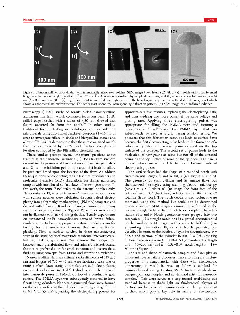
circumferential length, b, and height, h (see Figure 1a and b).The geometry of each cylinder and its surface flaws wascharacterized thoroughly using scanning electron microscopy(SEM) at a 52° tilt at 0° (to image the front face of thecylinder) and 180° (back face) rotation and at 86° tilt at 0°rotation (front face). The notch depth, a, and radius, r, wereestimated using this method but could not be determinedprecisely because SEM imaging cannot be performed at thenecessary angles relative to the notch for complete character-ization of a and r. Notch geometries were grouped into twocategories: (1) a straight notch or (2) a partial circumferentialnotch based on SEM images, with r equal to half of h (seeSupporting Information, Figure S1). Notch geometry wasdescribed in terms of the fraction of cylinder circumference, b ̅ =b/πD, and fraction of the cylinder height, h̅ = h/l. Resultingunitless dimensions were b ̅ = 0.10−0.50 (circumferential lengthof b = 40−200 nm) and h̅ = 0.02−0.07 (notch height h = 15−50 nm) (Figure 1).The size and shape of nanoscale samples and flaws play an
important role in failure processes; hence to compare fractureproperties in a nanomaterial with those with macroscopicdimensions, it would be wise to follow a standard fornanomechanical testing. Existing ASTM fracture standards aredesigned for large samples, and no standard exists for nanoscalesamples.25 This work serves as a step toward establishing thisstandard because it sheds light on fundamental physics offracture mechanisms in nanomaterials in the presence ofnotches, which play a key role in failure of macroscopic
Figure 1. Nanocrystalline nanocylinders with intentionally introduced notches. SEM images taken from a 52° tilt of (a) a notch with circumferentiallength b = 84 nm and height h = 47 nm (b ̅ = 0.23 and h ̅ = 0.06 when normalized by sample dimensions) and (b) a notch of b = 161 nm and h = 24nm (b ̅ = 0.54 and h̅ = 0.03). (c) Bright-field TEM image of plucked cylinder, with the boxed region represented in the dark-field image inset whichshows a nanocrystalline microstructure. The other inset shows the corresponding diffraction pattern. (d) SEM image of an unflawed cylinder.
Nano Letters Letter
dx.doi.org/10.1021/nl403453h | Nano Lett. 2013, 13, 5703−57095704

samples. The sample geometry in this work is appropriate fornanofracture testing because the surface flaws represent a majorstress concentrator at which failure initiation would be expectedin a typical macroscopic sample. The nc-Pt samples failed at∼3% strain and approximately 1% plastic strain with noobservable bending at the flaw.Sample preparation for TEM was performed by “plucking” a
tension sample with the InSEM (Nanomechanics, Inc.), an insitu SEM with an attached nanoindenter.26 To do this, thetension sample was fed into a custom-milled tungsten tensiongrip used as the nanoindenter tip, which is used to lift thesample off the growth substrate. The grips were in contact withthe sample on the underside of the tension head. The samplewas then gently lowered onto a TEM grid using the tensiongrips, and then the tension grip was detached from the tensionhead. Carbon is applied to the base of the sample using e-beamdeposition to glue the sample to the TEM grid. TEM revealedthe grain size to be 6 ± 3 nm with no significant variationacross sample volumes.Tension tests were performed in the InSEM using a custom-
milled diamond tension grip.27 Electroplated Pt cylinders showpoor adhesion to the underlying Au substrate, so a smallamount of W glue was applied to the base of the cylinder usingthe FEI Nova 200 dual beam system. Tension tests wereconducted at a constant strain rate of 0.01 s−1. SEM video wastaken during tension testing, and instrument compliances,changes in sample dimensions, and fracture locations weredetermined from the video. Measured load−displacement datawas converted to true stress−strain curves, after accounting forinstrument compliance. During in situ SEM mechanical teststhe samples were oriented such that the surface flaw was on theside, rather than the front or back faces, of the sample relativeto the imaging electron beam to observe the initiation of failure(see Figure 2). We found that 8 of 12 samples broke at thesurface flaw, and the remaining 4 broke away from the flaw (seeSI for in situ SEM movies). Stress−strain data for eachexperiment suggested brittle failure, with limited plasticdeformation and no noticeable necking (Figure 2a,d). Thedata showed no significant difference in ultimate tensilestrengths (UTS) of samples that broke at the flaw (UTS of1.8 ± 0.1 GPa), ones that broke away from the flaw (UTS of1.8 ± 0.2 GPa), and the unnotched samples. This strength is50% higher than that of similarly fabricated Pt nanopillarstested in compression, which is likely due to the higherdeformation strain rate (0.001 s−1 for compression vs 0.01 s−1
here) and the tension−compression asymmetry common to
nanocrystalline metals.24,28 Sample size-dependent weakeningappears in nanocrystalline Pt nanostructure when the samplesize to grain size ratio, D/d, falls below ∼5.24 Samples in thisstudy have a D/d of ∼20; hence, the measured strengths areindependent of sample size.Finite element modeling (FEM) was used to estimate the
stress concentration due to the external flaw on 11 of the 12experimentally tested nanocylinders to evaluate whether failurelocation and strength correlate with stress concentration at thenotch. The calculations showed that the stress concentrations atthe notches in the cylinders that broke at the notch to be higherthan those for notched samples that broke elsewhere for all butone sample. FEM simulations also revealed that elasticity-basedstress concentrations were not correlated with the experimentalUTS (see SI text, Figures S2−S4).SEM images revealed features with dimensions on the order
of grain size that populated the fracture surfaces, reminiscent oftypical dimpled fracture morphology of bulk nanocrystallinemetals29,30 (see SI text, Figure S5). This suggests theoccurrence of localized plasticity despite no evidence of globalnecking. The angle between the fracture surface relative to theloading axis and the curvature of the fracture surface across thewidth of the broken cylinder varied among the samples.The finding that 2/3 of the samples broke at the notch
suggests sensitivity of failure initiation to flaws. Both sets ofcylindersones that failed at the flaw and those that failedaway from itexhibited nearly identical fracture strengths,which implies flaw insensitivity in strength. To resolve thisapparent contradiction, we performed molecular dynamicssimulations of nc-Pt samples with notch and sample geometriessimilar to those in the experiments to reveal the mechanisticorigin of the experimentally observed deformation and failure.A periodic simulation cell (64 × 206 × 64 nm) was created
in which 648 “seeds” were randomly placed, and upon whichVoronoi tessellations are performed. The resulting Voronoipolyhedra were then filled with atoms in a perfect face-centeredcubic Pt crystal of random orientation to produce ananocrystalline structure with an average grain size of ∼14nm. Nanocrystalline Pt nanocylinders of diameter ∼43 nm anda film of thickness ∼20 nm were carved from this periodic bulknanostructure. MD simulations were performed using theLarge-scale Atomic/Molecular Massively Parallel Simulator(LAMMPS), where interactions between Pt atoms weredescribed using the Embedded Atom Method (EAM) potentialparametrized by Sheng et al.31−33 Periodic boundary conditionswere imposed along the nanocylinder axes and lengthwise along
Figure 2. Samples that broke at the flaw: (a) representative true stress−true strain plots from uniaxial tension tests, (b) SEM image of a preflawedsample, and (c) SEM image of the same sample after fracturing at the flaw. Samples that broke away from the flaw: (d) representative true stress−true strain plots from uniaxial tensile tests, (e) SEM image of a preflawed sample, and (f) SEM image of the same sample after fracturing away fromthe flaw.
Nano Letters Letter
dx.doi.org/10.1021/nl403453h | Nano Lett. 2013, 13, 5703−57095705

the film, while other surfaces were free. All of the structureswere equilibrated at 300 K before tensile loading was applied.34
Uniaxial tensile loading was applied at a constant true strainrate of 0.1 ns−1. During tensile loading, constant temperaturewas maintained using a Nose−́Hoover thermostat.35−38 Theatomic stresses were calculated based on the atomic virial stressin which the atomic volume was set to the Voronoi volumeassociated with each atom.A notch-free nanocylinder (Figure 3a) was created and used
as the starting structure for four nanocylinder samples with
notches of very different geometries. Two samples had roundednotches (b ̅ = 0.16 and h̅ = 0.03, Figure 3b; b ̅ = 0.2 and h ̅ = 0.03,Figure 3c), and two samples contained sharp notches (b ̅ = 0.23and h ̅ = 0.006, Figure 3d; b ̅ = 0.33 and h ̅ = 0.006, Figure 3e).Following equilibration at room temperature, the nanocylinderswere uniaxially stretched to failure.34 Before creating the notch,we first identified the fracture location in the notch-freenanocylinder and always placed the notches far away from thislocation.Figure 3 shows the stress−strain data for all five nano-
cylinders (a−e) and post-deformation samples that break awayfrom (f) and at (g) the notch. Simulations revealed that thesamples shown in Figure 3b and d broke away from the notch,in contrast to those in Figure 3c and e, which failed at thenotch. Regardless of the location of failure initiation, all stress−strain curves were remarkably similar, reaching a UTS of ∼3GPa, and then undergoing rapid strain softening even in themost extreme case in which the notch extended 1/3 across thesample diameter (Figure 3e). The nearly identical UTS in allfive samples demonstrates that the UTS was insensitive to thepresence of notches, and the occurrence of failure both at andaway from the notches suggests sensitivity of failure initiation toflaws, which corroborates the experiments.These experimental and computational results present
compelling evidence that the effects of flaws on deformationand failure of nanomaterials are significantly different fromthose in their coarse-grained and macroscopic counterparts. Togain further insight into what makes failure of nanomaterials
different in response to external notches, we examined theseprocesses at the atomic level. Figure 4 shows the spatial
distribution of atomic-level (virial) tensile stresses (σyy) near arounded notch (b ̅ = 0.2 and h ̅ = 0.03) and near a sharp notch(b ̅ = 0.23 and h ̅ = 0.006) at a 2.5% applied strain. The stressdistribution near both type of notches showed the presence of astrong stress concentration at the tip of the notch, which is ∼5times the average stress (a2−b2), and is sufficiently large totrigger highly localized plasticity at the notch. Partialdislocations were nucleated at the rounded notch root andpropagated across the grain, leaving stacking faults in their wake(Figure 4a3). Grain boundary sliding occurred in response tothe local stress at the sharper notch, which led to surface offsetswhere grain boundaries intersected the outer surface (Figure4b3, see SI for movies of stress evolution during fracture). Thecombination of grain boundary sliding and partial dislocationnucleation and propagation represents the intrinsic deformationmechanism of nanocrystalline Pt nanostructures.24 Grainboundary sliding generally occurs at a lower applied stressthan does dislocation nucleation but also depends on otherfactors such as the presence of neighboring grains withfavorable orientations and proximity to free surfaces. Thus,the specific plasticity mechanism active at the notch cannot bepredicted from notch geometry alone, although notch geometryinfluences the local stress.Surprisingly, the plastic activity near the notches was found
to be sufficient to reduce the local stress almost to thebackground stress level as shown in Figure 4a4−b4. Thesenotches no longer served as “hot spots” with regard to elevatedlocal stress. The notch roots became blunted, thereby shielding
Figure 3. Stress−strain curves of 5 simulation samples for (a) notch-free and notched samples with notch geometry with normalizedcircumferential width and height (b) b ̅ = 0.16 and h̅ = 0.03 (b = 21 nmand h = 5 nm), (c) b ̅ = 0.2 and h̅ = 0.03 (b = 30 nm and h = 5 nm),(d) b ̅ = 0.23 and h̅ = 0.006 (b = 31 nm and h = 1 nm), and (e) b ̅ =0.33 and h̅ = 0.006 (b = 44 nm and h = 1 nm). In the stress−straincurves, the orange circles mark the 2.5% and 8% strains at which theatomic stresses in Figure 2 were measured. The insets in a−e showmagnified views near the notches, and the blue lines indicate the notchdepths. (f−g) Examples of pillar fracture away from the notch (b ̅ =0.23; h ̅ = 0.006) and at the notch (b ̅ = 0.33 and h̅ = 0.006),respectively.
Figure 4. (a1−a2) Cross-sectional view of tensile stress (σyy) at 2.5%applied strain in simulated samples with rounded notch geometry (b ̅ =0.2 and h̅ = 0.03), and sharper notch geometry (b ̅ = 0.23 and h̅ =0.006). (a2−b2) Magnification at notch showing stress concentrationat notch tip. (a3−b3) Notch blunting by dislocation and grainboundary plasticity at 6.5% applied strain. (a4−b4) Stress contoursshow absence of stress concentrations near notches at 8% strainbecause of previously active plasticity mechanisms. In a3−b3, atomsare shown only if their central symmetry parameters differ from that ofthe perfect FCC crystal; the colors indicate the local symmetry.39
Atoms on twin boundaries, dislocations, and intrinsic and extrinsicstacking faults are shown in light blue, dark blue or green (dependingon dislocation type), orange, and light blue, respectively.
Nano Letters Letter
dx.doi.org/10.1021/nl403453h | Nano Lett. 2013, 13, 5703−57095706

the material near the notch from further stress increase.Subsequent localized plasticity in the samples occurred at otherstress concentrators in the sample, such as grain boundary triplejunctions. This analysis shows that even a severe notch with astrong initial stress concentration may not dominate failure in asample because plasticity mechanisms inherent to the nano-crystalline material can render the notch ineffective as a stressconcentration at later stages of deformation.Figure 5 presents a compelling example of localized plasticity
at the notch, which reduces the stress concentration by blunting
and exposes the intrinsic failure mechanism. Figure 5a1 showsan undeformed nanocrystalline slab geometry sample. Figure5a2 shows the same sample under an applied load, in which theemission of dislocations and grain boundary sliding led to largelocalized deformation at the notch and significant blunting. InFigure 5a3, a crack formed along a grain boundary at the notchroot and propagated unstably, which ultimately led to failure.Schematic illustrations (Figure 5b1−b3) of the change in notchgeometry during the deformation process show the process ofan initial, rounded notch elongating and blunting under tensionand finally fracturing along a grain boundary by the formationof a crack-like defect with characteristic size equal to the grainsize, d. The same failure mechanism can also lead to failureaway from the notch and applies to the deformation and failurein the unnotched samples. This is because a crack-like defectcan also form at an internal grain boundary (where the stresscannot be further relaxed due to the small crack size), whichcauses the adjacent grains to pull apart under tension (see SItext, Figure S6). The intrinsic failure strength of such a crack-like defect can be estimated using the Griffith equation, σf =√Eγρ/4ar0, in which E, γ, ρ, a, and r0 are the elastic modulus,surface energy, crack radius, crack length, and interatomicspacing, respectively. We assume that ρ = r0 for a sharp crackand a ≈ d, where d is the grain size. Using E = 160 GPa and γ =2 J/m2, we estimate the Griffith fracture strength to be 3 GPa.33
This is within a factor of 2 of the measured fracture strengthfrom experiments and simulations with no adjustableparameters. While Griffith theory applies only to brittlematerials, it is reasonable to use in the nanocrystalline samplesstudied here because no dislocations are generated near thegrain-sized crack (which is much smaller than the externalnotch) to plastically relax the crack stress field and dissipateenergy.The fundamental picture of failure in nanocrystalline
nanostructures with surface flaws that emerges from experi-ments and simulations is that the competition between stressconcentrators due to external flaws and intrinsic microstructuralfeatures governs failure strength and location. The samplesstudied here contain a statistical distribution of internal stressconcentrators associated with the microstructure, as well as anexternal stress concentration in the form of the notch. Thedominant internal stress concentrators in these nanocrystallinesamples are grain boundary triple junctions. Such features areubiquitous within nanocrystalline samples with the samplediameter large compared to the grain size. The strength oftriple junctions as stress concentrators depends on theorientation of the sliding grain boundaries relative to the loadas well as on the orientation of the slip systems within thegrains for dislocation nucleation. This gives rise to a statisticaldistribution of stress concentrators associated with micro-structural features. As the sample is loaded in tension, theinternal or external feature with the highest stress concentrationis activated and reaches a local stress at which it either relaxesplastically or breaks. If relaxation occurs at this site, thissequence of events repeats at the site of the next highest stressconcentration. This process continues to cascade until theactive site cannot relax, and fracture ensues.Samples tend to fail at the external flaw because the surface
notch is generally the site with either the highest or one of thehighest initial stress concentrations. In samples where failureoccurred at the flaw, the failure criteria was first met at theexternal notch, prior to any plasticity mechanism reducing thelocal stress at the external flaw to the level of the next weakestsite. Grain boundary sliding occurs more easily at the flawbecause of the initially high local stress at this location, whichmeans that the intrinsic failure mechanism is more likely tooperate at this location rather than elsewhere in the sample.A direct consequence of such a failure mechanism is flaw
insensitivity in strength because the same intrinsic failuremechanism leads to failure, regardless of whether failure occursat or away from the notch. Since the fundamental failuremechanisms are the same in the presence or absence ofnotches, the UTS is insensitive to exactly where the failureprocess starts. The cascade of stress relaxation at stressconcentrators via localized plastic deformation dictates thatthe stress concentration at these locations reaches similar levels,which gives rise to the narrow range of UTS measured inexperiment and simulation. This phenomenon is unique tonanocrystalline, nanoscale solids because large stress concen-trations can be plastically relaxed (via localized deformation),but those associated with the nanoscale microstructure featurescannot be relaxed because they are too small for dislocationnucleation (and localized plasticity). In a macroscale nano-crystalline system, the UTS can be modulated by introductionof very large, sharp flaws that create plastic zones that are toolarge to be relaxed by local plastic deformation. In such cases,the ultimate failure mode is likely to be more ductile than in ourexperiments on nanosamples, which show brittle fracture.
Figure 5. Cross-sectional view of intergranular fracture at the notch tipin a Pt polycrystalline film. (a1) Notch at 0% strain, (a2) at 7% strainwhere the notch is blunted by local plasticity emanates from the notchtip, and (a3) 11% strain where intergranular fracture initiates at thenotch. Atoms are colored based on their structural type as determinedby common neighbor analysis: blue for atoms at lattice positions,green for atoms at stacking faults, and yellow for atoms at grainboundaries.40 (b1−b3) The corresponding schematics showing theundeformed notch geometry, notch blunting, and widening andintergranular fracture occurring at a grain boundary with characteristicsize d.
Nano Letters Letter
dx.doi.org/10.1021/nl403453h | Nano Lett. 2013, 13, 5703−57095707

Although the MD simulations demonstrate excellentqualitative agreements with experimental results, quantitativedifferences exist. MD simulations show a moderately ductilefracture on the scale of the grain size, while the experimentssuggest a “brittle” fracture process. This discrepancy could beattributed to the differences in grain sizes (6 nm in experimentsvs 14 nm in simulations), the number and orientation of thegrains across the cylinder diameter and ahead of notches, andfrom the much higher strain rates in the simulations.Nevertheless, the experiments and simulations unambiguouslydemonstrate that failure initiation in nanomaterials isdetermined by intrinsic microstructural failure mechanismsand that the UTS is insensitive to the presence of notches.The results presented here can be summarized as: (1) flaw
insensitivity in strength: strength does not depend on whetherfailure initiates at an external flaw or within the microstructure,and (2) flaw sensitivity in fracture location: most nc-Ptnanocylinders broke at the prefabricated flaws regardless offracture strength as long as the flaw was sufficiently large/sharp.These observations can be explained through competitionbetween internal microstructural features and the external flaw.Brittle failure occurs at a constant stress, independent of thenotch provided that the stress-field at the notch is small enoughthat ductile fracture does not occur and that the microstructuralfeatures (crack nucleation sites) are too small to emitdislocations (plastically relax). In classes of materials whereplastic deformation cannot occur easily (e.g., ceramics), localplastic relaxation at the notch tip may not be possible, andhence such nanomaterials may still fail at a notch-dependentultimate stress. In the case of nanocrystalline Pt nanostructures,nucleating dislocations is fairly easy; in other nanomaterials, it ispossible that non-dislocation plasticity could play a similarrolefor example, polymer flow between ceramic units, as inmany strong and tough biological materials.The competition between stress concentrations within the
sample naturally leads to flaw sensitivity in failure initiationlocation, because incipient deformation and subsequent failureoccur at the position of the stress concentration which firstsatisfies the failure criteria. The localized plasticity in thevicinity of stress concentrators, that is, triple junctions or flaws,tends to reduce the initially present stress concentrations,which leads to a more effective competition of the multiplestress concentrators throughout the sample volume. Thisprocess results in similar fracture strengths for a wide rangeof flaw shapes and sizes, which is manifested as flaw insensitivityin strength.Major external flaws do not necessarily reduce the strength of
nanoscale and nanostructured materials yet may still serve assites of failure initiation if the intrinsic failure criterion isreached because of the high local stress compared to stresses atinternal, microstructural features. The high strength intrinsic tomany nanostructures can be maintained while increasingfracture toughness, or resistance to failure at flaws, throughmicrostructural toughening mechanisms. These findings shedlight on failure processes in nanomaterials, which commonlyshow significant deviations from mechanical behavior expectedfrom classical continuum theory. Microstructure and externalsize information must also be included when predicting failurein nanomaterials. The present results suggest that futurenanofracture testing be performed with careful consideration ofmicrostructural effects as well as well-defined and characterizedsample and notch geometries. Sample and notch geometriesappropriate for application of classical continuum theories may
not be accessible in nanostructures where internal, micro-structural features also have an important influence on failure.
■ ASSOCIATED CONTENT*S Supporting InformationModeling of notch geometry, finite element modeling ofnotched cylinders, fracture surface morphology, and crackformation at internal grain boundary, plus molecular dynamicsand in situ SEM movies. This material is available free of chargevia the Internet at http://pubs.acs.org.
■ AUTHOR INFORMATIONCorresponding Author*Phone: 626-395-4127; e-mail: [email protected] authors declare no competing financial interest.
■ ACKNOWLEDGMENTSX.W.G. is grateful for financial support from the NationalDefense Science and Engineering Graduate (NDSEG) Fellow-ship, 32 CFR 168a. J.R.G. acknowledges the financial support ofthe National Science Foundation (DMR-1204864). X.W.G. andJ.R.G. thank the Kavli Nanoscience Institute at Caltech for theavailability of critical cleanroom facilities. We thank V.Deshpande and D. Jang for helpful discussion and D. Jangand C. Garland for TEM assistance. The authors gratefullyacknowledge the financial support from the Agency for Science,Technology and Research (A*STAR), Singapore and the use ofcomputing resources at the A*STAR Computational ResourceCentre, Singapore.
■ REFERENCES(1) Currey, J. D. Mechanical-Properties of Mother of Pearl inTension. Proc. R. Soc. B: Biol. Sci. 1977, 196, 443−463.(2) Fratzl, P.; Weinkamer, R. Nature’s hierarchical materials. Prog.Mater. Sci. 2007, 52, 1263−1334.(3) Yu, M. F.; Lourie, O.; Dyer, M. J.; Moloni, K.; Kelly, T. F.; Ruoff,R. S. Strength and breaking mechanism of multiwalled carbonnanotubes under tensile load. Science 2000, 287, 637−640.(4) Lee, C.; Wei, X. D.; Kysar, J. W.; Hone, J. Measurement of theelastic properties and intrinsic strength of monolayer graphene. Science2008, 321, 385−388.(5) Garel, J.; Leven, I.; Zhi, C. Y.; Nagapriya, K. S.; Popovitz-Biro, R.;Golberg, D.; Bando, Y.; Hod, O.; Joselevich, E. Ultrahigh TorsionalStiffness and Strength of Boron Nitride Nanotubes. Nano Lett. 2012,12, 6347−6352.(6) Bertolazzi, S.; Brivio, J.; Kis, A. Stretching and Breaking ofUltrathin MoS2. ACS Nano 2011, 5, 9703−9709.(7) Lu, L.; Chen, X.; Huang, X.; Lu, K. Revealing the MaximumStrength in Nanotwinned Copper. Science 2009, 323, 607−610.(8) Uchic, M. D.; Dimiduk, D. M.; Florando, J. N.; Nix, W. D.Sample dimensions influence strength and crystal plasticity. Science2004, 305, 986−989.(9) Vigolo, B.; et al. Macroscopic fibers and ribbons of orientedcarbon nanotubes. Science 2000, 290, 1331−1334.(10) Hao, S.; et al. A transforming metal nanocomposite with largeelastic strain, low modulus, and high strength. Science (New York, N.Y.)2013, 339, 1191−1194.(11) Dugdale, D. S. Yielding of Steel Sheets Containing Slits. J. Mech.Phys. Solids 1960, 8, 100−104.(12) Hertzberg, R. W. Deformation and Fracture Mechanics ofEngineering Materials; Wiley: New York, 1995.(13) Gao, H. J.; Ji, B. H.; Jager, I. L.; Arzt, E.; Fratzl, P. Materialsbecome insensitive to flaws at nanoscale: Lessons from nature. Proc.Natl. Acad. Sci. U.S.A. 2003, 100, 5597−5600.
Nano Letters Letter
dx.doi.org/10.1021/nl403453h | Nano Lett. 2013, 13, 5703−57095708

(14) Buehler, M. J.; Yao, H. M.; Gao, H. J.; Ji, B. H. Cracking andadhesion at small scales: atomistic and continuum studies of flawtolerant nanostructures. Modell. Simul. Mater. Sci. Eng. 2006, 14, 799−816.(15) Giesa, T.; Pugno, N. M.; Buehler, M. J. Natural stiffeningincreases flaw tolerance of biological fibers. Phys. Rev. E 2012, 86,041902.(16) Kumar, S.; Li, X. Y.; Haque, A.; Gao, H. J. Is StressConcentration Relevant for Nanocrystalline Metals? Nano Lett.2011, 11, 2510−2516.(17) Zhang, T.; Li, X. Y.; Kadkhodaei, S.; Gao, H. J. Flaw InsensitiveFracture in Nanocrystalline Graphene. Nano Lett. 2012, 12, 4605−4610.(18) Khare, R. M.; Mielke, S. L.; Paci, J. T.; Zhang, S. L.; Ballarini, R.;Schatz, G. C.; Belytschko, T. Coupled quantum mechanical/molecularmechanical modeling of the fracture of defective carbon nanotubes andgraphene sheets. Phys. Rev. B 2007, 75, 075412.(19) Mielke, S. L.; et al. The role of vacancy defects and holes in thefracture of carbon nanotubes. Chem. Phys. Lett. 2004, 390, 413−420.(20) Kumar, S.; Haque, M. A.; Gao, H. Notch insensitive fracture innanoscale thin films. Appl. Phys. Lett. 2009, 94, 253104.(21) Wurster, S.; Motz, C.; Pippan, R. Characterization of thefracture toughness of micro-sized tungsten single crystal notchedspecimens. Philos. Mag. 2012, 92, 1803−1825.(22) Iqbal, F.; Ast, J.; Goken, M.; Durst, K. In situ micro-cantilevertests to study fracture properties of NiAl single crystals. Acta Mater.2012, 60, 1193−1200.(23) Kupka, D.; Lilleodden, E. T. Mechanical Testing of Solid-SolidInterfaces at the Microscale. Exp. Mechanics 2012, 52, 649−658.(24) Gu, X. W.; Loynachan, C. N.; Wu, Z. X.; Zhang, Y. W.;Srolovitz, D. J.; Greer, J. R. Size-Dependent Deformation ofNanocrystalline Pt Nanopillars. Nano Lett. 2012, 12, 6385−6392.(25) Wilson, C. D.; Landes, J. D. Fracture toughness testing withnotched round bars; ASTM STP 1360; ASTM: West Conshohocken,PA, 2000; Vol. 30, ID STP13396S.(26) Jang, D.; Li, X.; Gao, H.; Greer, J. R. Deformation mechanismsin nanotwinned metal nanopillars. Nat. Nanotechnol. 2012, 7, 594−601.(27) Kim, J. Y.; Jang, D. C.; Greer, J. R. Insight into the deformationbehavior of niobium single crystals under uniaxial compression andtension at the nanoscale. Scr. Mater. 2009, 61, 300−303.(28) Jang, D. C.; Greer, J. R. Size-induced weakening and grainboundary-assisted deformation in 60 nm grained Ni nanopillars. Scr.Mater. 2011, 64, 77−80.(29) Dalla Torre, F.; Van Swygenhoven, H.; Victoria, M. Nano-crystalline electrodeposited Ni: microstructure and tensile properties.Acta Mater. 2002, 50, 3957−3970.(30) Hasnaoui, A.; Van Swygenhoven, H.; Derlet, P. M. Dimples onnanocrystalline fracture surfaces as evidence for shear plane formation.Science 2003, 300, 1550−1552.(31) Plimpton, S. Fast Parallel Algorithms for Short-RangeMolecular-Dynamics. J. Comput. Phys. 1995, 117, 1−19.(32) Daw, M. S.; Baskes, M. I. Embedded-Atom Method - Derivationand Application to Impurities, Surfaces, and Other Defects in Metals.Phys. Rev. B 1984, 29, 6443−6453.(33) Sheng, H. W.; Kramer, M. J.; Cadien, A.; Fujita, T.; Chen, M. W.Highly optimized embedded-atom-method potentials for fourteen fccmetals. Phys. Rev. B 2011, 83, 134118.(34) Wu, Z. X.; Zhang, Y. W.; Jhon, M. H.; Gao, H. J.; Srolovitz, D. J.Nanowire Failure: Long = Brittle and Short = Ductile. Nano Lett.2012, 12, 910−914.(35) Nose, S. A Unified Formulation of the Constant TemperatureMolecular-Dynamics Methods. J. Chem. Phys. 1984, 81, 511−519.(36) Nose, S. A Molecular-Dynamics Method for Simulations in theCanonical Ensemble. Mol. Phys. 1984, 52, 255−268.(37) Hoover, W. G. Constant-Pressure Equations of Motion. Phys.Rev. A 1986, 34, 2499−2500.
(38) Melchionna, S.; Ciccotti, G.; Holian, B. L. Hoover NPTDynamics for Systems Varying in Shape and Size. Mol. Phys. 1993, 78,533−544.(39) Kelchner, C. L.; Plimpton, S. J.; Hamilton, J. C. Dislocationnucleation and defect structure during surface indentation. Phys. Rev. B1998, 58, 11085−11088.(40) Faken, D.; Jonsson, H. Systematic analysis of local atomicstructure combined with 3D computer graphics. Comput. Mater. Sci.1994, 2, 279−286.
Nano Letters Letter
dx.doi.org/10.1021/nl403453h | Nano Lett. 2013, 13, 5703−57095709