microstructure and device performance of thin film light ... · microstructure and device...
TRANSCRIPT

007) 3787–3796www.elsevier.com/locate/tsf
Thin Solid Films 515 (2
Microstructure and device performance of thin film light emitting polymers
Piyachat Yimsiri b,⁎, Malcolm R. Mackley a
a Department of Chemical Engineering, University of Cambridge, Pembroke Street, Cambridge CB2 3RA, UKb Department of Chemical Engineering, Faculty of Engineering, Burapha University, Saensook, Maung, Chonburi 20131, Thailand
Received 8 August 2005; received in revised form 27 September 2006; accepted 27 September 2006Available online 24 October 2006
Abstract
In this paper, the performance of polymer light emitting diodes (PLEDs) was investigated and related to their thin film morphology. Twomethods were used to cast the thin film, i.e. spin coating and dip coating. The film morphology was controlled by different film formationconditions, e.g. spin speed and withdrawal speed, as well as different solution properties, e.g. polymer molecular weight and solvent. Phaseseparation was inspected using both optical microscopy and an atomic force microscopy. The device performances of interest were characterisedby measuring optical response, the Commission Internationale de l'Eclairage Chromaticity, electrical characteristics, and device lifetime. Thestudy has established that a high efficiency PLED can be achieved by using a blend of electron transporting emitter and a hole transportingpolymer. The device prepared from the blend shows a low turn-on voltage, a large current density, a high efficiency, and an acceptable lifetime.The result shows that light emitting polymer film morphology is crucial in determining the device performance. As solvent evaporation rateincreases, phase separation reduces to a fine-scale. The device efficiency decreases with a reduction of degree of phase separation while thelifetime enhances. It is likely that there is an optimum degree of phase separation for device optimisation (high efficiency and long lifetime). Inaddition, it was established that both dip and spin coating were effective fabrication processes.© 2006 Elsevier B.V. All rights reserved.
Keywords: Polymer light emitting diode; Atomic force microscopy; Surface structure; Electroluminescence efficiency
1. Introduction
Polymer light emitting diodes (PLEDs) are making atransition from a laboratory scale to an industrial level and anunderstanding of the effect of processing on device performanceis now paramount. The device performance is mainly concernedwith four factors, namely, (i) device efficiency and brightness,(ii) power consumption, (iii) device lifetime, and (iv) colourcontrol [1]. The structure of the PLEDs shown in Fig. 1 consistsof several elements, i.e. an emissive component (light emittingpolymer, LEP), a hole transporting layer (poly(3,4-ethylenediox-ythiophene) dopedwith polystyrene sulphonic acid, PEDOT:PSS),and two electrodes (indium–tin oxide anode and metal cathode);therefore, achieving good device performance depends on severalissues, such as electrode characteristics, polymer/electrode inter-facial effect, and LEPmorphological and optoelectronic properties.
⁎ Corresponding author. Tel.: +66 3874 5900x3351; fax: +66 38745900x3350.
E-mail address: [email protected] (P. Yimsiri).
0040-6090/$ - see front matter © 2006 Elsevier B.V. All rights reserved.doi:10.1016/j.tsf.2006.09.043
Accomplishing balanced electron-hole injection and perfectrecombination of the charge carriers would ensure the optimumperformance of PLEDs. Various approaches have been intro-duced to control charge injection and charge balance, such asappropriate selection of anode and cathode, surface modificationof the electrodes, insertion of hole-injection layers, and use ofheterostructure or polymer blends. For an effective holeinjection, the anode should have a relatively large work functionmatching the highest occupied molecular orbital (HOMO) levelof the LEP, whereas the cathode should have a lowwork functionto ensure effective electron injection into the lowest unoccupiedmolecular orbital (LUMO) level of the LEP. Indium–tin oxide(ITO) has proved to be a suitable anode [2–4]. However, Scottet al. [5] found that ITO acts as a source of oxygen which leads tooxidation causing device aging; therefore, the insertion of thehole-injection-transporting layer is necessary to avoid the directcontact between the emissive LEP layer and ITO as well as toenhance the balanced charge injection [6–9]. Lowwork functionmetals (e.g. calcium andmagnesium) are suitable for the electroninjection electrode (cathode). However, these materials, in

Fig. 1. Basic structure of PLEDs.
3788 P. Yimsiri, M.R. Mackley / Thin Solid Films 515 (2007) 3787–3796
particular calcium, are highly reactive and therefore verysusceptible to oxidation, causing the device instability [10]. Inorder to improve the device stability, the cathode is often cappedwith atmospherically stable metals, e.g. aluminium and silver[11–14].
This particular study focuses on the processing andmorphology of the LEP layer. Other parameters of the deviceconstruction have been kept strictly identical in order to facilitatecomparison.
Polymer blends can broaden emission spectra, alter theelectronic properties, and improve the device performance[15,16]. Such aspects are an outcome of changes in the structureof the thin films. Consequently, an understanding of the mecha-nism that affects the morphology of the LEP film is crucial andbeneficial to PLED manufacture. Phase separation often occurswhen using blends of LEPs containing monomers of signifi-cantly different chemical structures. Various techniques havebeen used to study the morphology of the LEP film [17–19].However, very little information about the relationship betweenthe morphology of the emissive LEP film and the deviceperformance is available. Cina studied the PLED performanceprepared from blends of hole-transporting polyfluorene (poly(9,9-dioctylfluorene-co-N-(4-butylphenyl)diphenylamine),TFB) and poly(9,9-dioctylfluorene-co-benzothiadiazole)(F8BT) and found that increasing the polymer molecularweight results in large-scale phase separation, however thedevice efficiency also increases. The polymer blends used inthis paper are similar to those studied by Cina, Morgado [17],and Kim et al. [20] where TFB or poly(9,9-dioctylfluorene) isreplaced byHost 1 (a poly(9,9-dioctylfluorene)–TFBcopolymer).
2. Materials and device fabrication
Three LEP solutions used were blends of two different LEPsystems, which are poly(9,9-dioctylfluorene-co-benzothiadia-zole) (F8BT) and poly(9,9-dioctylfluorene-co-TFB (Host 1),with a weight ratio of approximately 5:95.Mixed isomers xylene
Table 1Details of LEP solutions
Solution Host 1 (DP) F8BT (DP) Concentration (% w/v) Solvent
1 52 108 1.6 Xylene2 52 295 1.6 Xylene3 163 295 1.6 Xylene4⁎ – – 1.2 Toluene
⁎Solution 4 is a reference solution.
was used as a solvent and the blends were made at theconcentration of 1.6% w/v (1.6 grams of polymer dissolved in100 ml of solvent). Details of the solutions with a degree ofpolymerisation (DP) of the LEPs are summarised in Table 1. Areference solution (solution 4), which was used at the CambridgeDisplay Technology, was prepared from the blend of Host 1 andF8BT at the concentration of 1.2% w/v using toluene as asolvent. Due to confidentiality, DPs of the polymer systemcannot be revealed.
A 25×25 mm2 commercial patterned ITO-coated glass wasused as a substrate. The substrate was patterned to form 8 pixelswith the area of each pixel of 2×12 mm2. Prior to the fabricationprocess, the substrates were cleaned by oxygen plasma. The50 nm thick hole-injection-transporting layer of PEDOT:PSS wasprepared using a spin coating process [21]. After the coatingprocess, the substrate was baked on a hot plate for 10 min to drythe PEDOT:PSS layer. A uniform LEP film of approximately70 nm thick was coated on top of the PEDOT:PSS layerimmediately by a spin or dip coating process. For the spin coatingprocess, a spin coater usedwas a Karl Suss RC 8GYRSET, whichcan operate with a rotating cover called a GYRSET. TheGYRSET system is a closed chamber that creates a solvent-richenvironment above the substrate. The evaporation rate of thepolymer solution can thus be controlled by the use of theGYRSET. The spinning with GYRSET is henceforth referred toas ‘slow evaporation’ whereas the spinning without GYRSET isreferred to as ‘fast evaporation’. For the dip coating process, aStable Microsystems Texture Analyser (TA-XT2) was used in theexperiment for the dip coating process and two drying methodswere applied to the polymer films, i.e. ambient drying and hot-airdrying, in order to investigate the effect of solvent evaporation.For ambient drying, the substrate was left in a vertical orientationin a fume cupboard for 60 min to dry. For hot-air drying, hot airfrom a hair dryer was blown onto the substrate during thewithdrawal process. A diffuser was attached to the head of the hairdryer to achieve uniform distribution of the hot air. The hot air hada temperature of around 50–60 °C and the blowing speed wasapproximately 6 m/s. The aim of hot-air drying is to minimise theoverlap between the liquid draining and film drying stages, whichcan cause a non-uniform film thickness. In the followingdiscussion, the ambient drying and hot-air drying are referred toas slow and fast drying, respectively. The spin and withdrawalspeeds were adjusted accordingly in order to obtain the filmthickness of approximately 70 nm. Details in relation to therelationship between film thickness and spin and withdrawalspeeds as well as the film thickness measurement can be foundfrom Yimsiri and Mackley [21].

Fig. 3. Film microstructure: (a) an optical microscopic image under excitation at488 nm and (b) threshold image obtained from Scion.
3789P. Yimsiri, M.R. Mackley / Thin Solid Films 515 (2007) 3787–3796
After the deposition of the emissive film, the substrate waskept in an opaque box immediately prior to subsequent cathodeevaporation to prevent exposure to light, humidity, and contami-nation by dust. Calcium was used as a cathode because it has alow work function to match the LUMO level of the polymer.The deposition of the cathode was done by a thermal evapo-ration at 10−4 Pa to achieve the thickness of 50 nm. A protectinglayer of aluminium of at least 500 nm thick was capped on thecalcium layer using the same method. Finally, metal legs wereassembled and the device was encapsulated using a glass coverslide with the same size of 25×25 mm2 and epoxy resin. Afterthe encapsulation, the device was kept in a glove box for at least12 h to allow the epoxy glue to set before performing any tests.Both metal leg assembling and encapsulation processes must becarried out under a dry nitrogen atmosphere in the glove box. Atleast ten devices were made from the same material andfabrication process to ensure the reproducibility.
3. Morphological characterisation
Phase separation was investigated using an Olympus BX60optical microscope as well as a Digital Instruments atomic forcemicroscope (AFM). In order to achieve the best possible contrastbetween phaseswith the opticalmicroscope, a 488 nmwavelengthlight source was used to excite the thin films. This wavelength canbe absorbed by F8BT, but not by Host 1 (see absorption spectra inFig. 2). Therefore, the wavelength can selectively excite F8BT,leading to the appearance of bright and dark areas according totheir enrichment in F8BTas show in Fig. 3(a). A Charge-CoupledDevice (CCD) camera was attached to the microscope to obtaindigital images. Several images were taken from different areas ofthe film and the images were analysed using a Scion Imagesoftware. The Scion Image is a PC version of the NIH-imagesoftware, which is a public domain image processing and analysisprogramme developed by the U.S. National Institutes of Health.This software uses the grey-scale to distinguish the area of interestfrom the background as shown in Fig. 3(b) and it can be used tomeasure area, diameter, perimeter, length, ellipse major axis, andellipse minor axis of user defined regions. The degree of F8BT-rich phase was of interest and used to quantify the level of phaseseparation. As a result, the area ratio of the bright phase to the total
Fig. 2. Absorption spectra of Host 1 and F8BT.
area was determined using the software. An average value of thearea ratios from several images was used to represent the phaseratio of an individual film. A higher F8BT-rich phase ratio indi-cates a higher degree of phase separation.
The analysis using the AFM was also carried out on somesamples to verify the results of the optical microscopy at ahigher resolution. The AFM used is a Dimension 3100 linked toa NanoScope III controller from Digital Instrument (VeecoInstruments). For each film, the areas of 1×1 and 10×10 μm2
were scanned using the tapping™ mode at an engagement setpoint of 2 Volts to minimise damage to the samples [22]. Singlecrystal silicon tip with a spring constant of 60 N m−1 was used.In these experiments, the scan rate and number of samples usedwere 0.5 Hz and 512, respectively for 1×1 μm2 scans and 1 Hzand 512, respectively, for 10×10 μm2 scans. The RMSroughness is the standard deviation of the height of the surface,which is given by:
RMS ¼
ffiffiffiffiffiffiffiffiffiffiffiffiffiffiffiffiffiffiffiffiffiffiffiffiffiffiffiffiffiXNi¼1
ðZi−ZavgÞ2
N
vuuuut ð1Þ
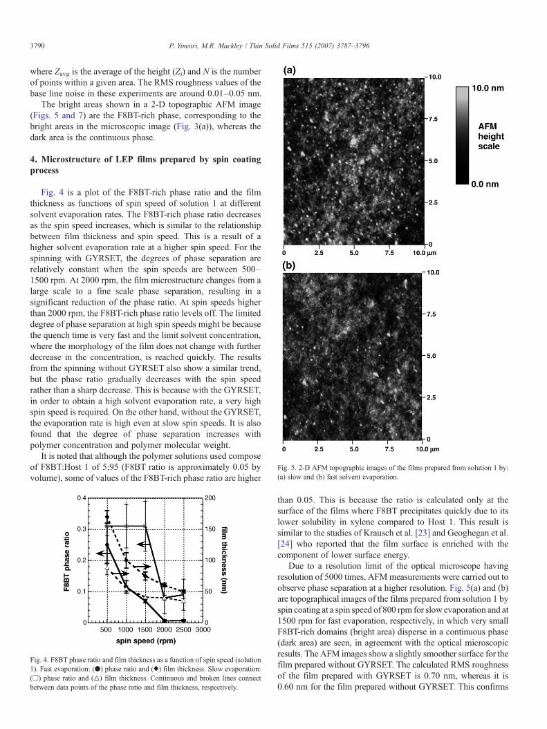
Fig. 5. 2-D AFM topographic images of the films prepared from solution 1 by:(a) slow and (b) fast solvent evaporation.
3790 P. Yimsiri, M.R. Mackley / Thin Solid Films 515 (2007) 3787–3796
where Zavg is the average of the height (Zi) and N is the numberof points within a given area. The RMS roughness values of thebase line noise in these experiments are around 0.01–0.05 nm.
The bright areas shown in a 2-D topographic AFM image(Figs. 5 and 7) are the F8BT-rich phase, corresponding to thebright areas in the microscopic image (Fig. 3(a)), whereas thedark area is the continuous phase.
4. Microstructure of LEP films prepared by spin coatingprocess
Fig. 4 is a plot of the F8BT-rich phase ratio and the filmthickness as functions of spin speed of solution 1 at differentsolvent evaporation rates. The F8BT-rich phase ratio decreasesas the spin speed increases, which is similar to the relationshipbetween film thickness and spin speed. This is a result of ahigher solvent evaporation rate at a higher spin speed. For thespinning with GYRSET, the degrees of phase separation arerelatively constant when the spin speeds are between 500–1500 rpm. At 2000 rpm, the film microstructure changes from alarge scale to a fine scale phase separation, resulting in asignificant reduction of the phase ratio. At spin speeds higherthan 2000 rpm, the F8BT-rich phase ratio levels off. The limiteddegree of phase separation at high spin speeds might be becausethe quench time is very fast and the limit solvent concentration,where the morphology of the film does not change with furtherdecrease in the concentration, is reached quickly. The resultsfrom the spinning without GYRSET also show a similar trend,but the phase ratio gradually decreases with the spin speedrather than a sharp decrease. This is because with the GYRSET,in order to obtain a high solvent evaporation rate, a very highspin speed is required. On the other hand, without the GYRSET,the evaporation rate is high even at slow spin speeds. It is alsofound that the degree of phase separation increases withpolymer concentration and polymer molecular weight.
It is noted that although the polymer solutions used composeof F8BT:Host 1 of 5:95 (F8BT ratio is approximately 0.05 byvolume), some of values of the F8BT-rich phase ratio are higher
Fig. 4. F8BT phase ratio and film thickness as a function of spin speed (solution1). Fast evaporation: (●) phase ratio and (♦) film thickness. Slow evaporation:(□) phase ratio and (▵) film thickness. Continuous and broken lines connectbetween data points of the phase ratio and film thickness, respectively.
than 0.05. This is because the ratio is calculated only at thesurface of the films where F8BT precipitates quickly due to itslower solubility in xylene compared to Host 1. This result issimilar to the studies of Krausch et al. [23] and Geoghegan et al.[24] who reported that the film surface is enriched with thecomponent of lower surface energy.
Due to a resolution limit of the optical microscope havingresolution of 5000 times, AFMmeasurements were carried out toobserve phase separation at a higher resolution. Fig. 5(a) and (b)are topographical images of the films prepared from solution 1 byspin coating at a spin speed of 800 rpm for slow evaporation and at1500 rpm for fast evaporation, respectively, in which very smallF8BT-rich domains (bright area) disperse in a continuous phase(dark area) are seen, in agreement with the optical microscopicresults. The AFM images show a slightly smoother surface for thefilm prepared without GYRSET. The calculated RMS roughnessof the film prepared with GYRSET is 0.70 nm, whereas it is0.60 nm for the film prepared without GYRSET. This confirms

Fig. 7. 2-D AFM topographic images of the films prepared from solution 2 by:(a) slow and (b) fast solvent evaporation.
3791P. Yimsiri, M.R. Mackley / Thin Solid Films 515 (2007) 3787–3796
that less degree of phase separation occurs when the solventevaporation increases.
5. Microstructure of LEP Films prepared by dip coatingprocess
Fig. 6 is a plot of the phase separation and film thickness asfunctions of withdrawal speed at different solvent evaporationrates. For ambient drying, the F8BT-rich phase ratio increaseswith the withdrawal speed, similar to the relationship betweenfilm thickness and withdrawal speed. The F8BT-rich rationotably increases when the withdrawal speed increases from 0.1to 0.3 mm/s and becomes relatively constant at higher speeds. Incontrast, the higher withdrawal speed results in the lower degreeof phase separation for hot-air drying. This is because at higherspeed, the onset of drying occurs more rapidly. It was also foundthat the phase separation increase with an increase in solutionconcentration and polymer molecular weight, similar to theresults obtained from the spin coating process.
The results obtained from AFM measurements confirm thesignificant effects of solvent evaporation rates. Fig. 7(a) and (b)show the topographic images of the films prepared fromsolution 2 by the dip coating process at the withdrawal speed of0.1 mm/s with ambient and hot-air drying, respectively. TheRMS roughness of the film prepared with ambient drying is2.54 nm whereas it is 0.66 nm for the hot-air drying.
6. Device characterisation
6.1. Optical characteristics
The optical characterisation involved photoluminescence(PL) spectra and refractive index measurement. The PL spectrawere collected using an Oriel charge coupled device (CCD)matrix spectrograph. The film was excited by a laser with thewavelength of 325 nm. The PL efficiency was calculated by acomparison between the absorbed number of photons with theemitted number of photons using an integrating sphere which is
Fig. 6. F8BT phase ratio and film thickness as a function of withdrawal speed(solution 2). Fast drying: (●) phase ratio and (♦) film thickness. Slow drying:(□) phase ratio and (▵) film thickness. Continuous and broken lines connectbetween data points of the phase ratio and film thickness, respectively.
purged with nitrogen to avoid photooxidation. Further details ofthe PL quantum efficiency measurement can be found inGreenham et al. [25] and de Mello et al. [26].
The refractive index of the film was measured using a J. A.Woollam M-2000™ diode-array rotating-compensator
Table 2PL efficiency (325 nm) and refractive index (632 nm) of films prepared bydifferent techniques
Fabricationprocess
Avg. PLefficiency
PLefficiencyS.D.
Avg.refractiveindex
Refractiveindex S.D.
Spin coating(w/o GYRSET)
55 2 1.601 0.001
Dip coating(ambientduring)
52 3 1.599 0.007
Dip coating (hot-air drying)
51 3 1.600 0.001

Fig. 8. (a) CIE chromaticity diagram and (b) insert of Fig. 8(a).
Fig. 9. I–V–L characte
3792 P. Yimsiri, M.R. Mackley / Thin Solid Films 515 (2007) 3787–3796
ellipsometer with a xenon lamp source. Ellipsometry is atechnique that measures the change of polarisation of light as afunction of incident angle and wavelength. The ratio ofreflection coefficients for p-(in the plane of incidence) and s-(perpendicular to the plane of incidence) polarised light wererecorded. Together with incidence transmission measurements,a non-linear regression analysis was performed by the WVASE32 software to determine the refractive index. More details ofthe ellipsometric determination can be found in Woollam et al.[27] and Ramsdale and Greenham [28].
The measured PL efficiency and refractive indices aresummarised in Table 2. The films prepared by the dip coatingwith the two drying methods show similar PL efficiencies (51–52%) which is slightly less than that of the film prepared by spincoating process (55%). The refractive indices at 632 nm of thethree films have similar value of around 1.6. Therefore, it can beconcluded that the optical properties of the films prepared byspin and dip coating techniques are generally very similar.
6.2. The Commission Internationale de l'Eclairage Chromaticity
Electroluminescence (EL) spectra were measured using anOcean Optics spectrometer and similarly to the PL spectra, thefilms prepared by the spin and dip coating processes havesimilar EL spectra. The Commission Internationale de l'Eclai-rage Chromaticity (CIE) co-ordinates of the devices are rela-tively similar with x ranging from 0.38 to 0.43 and y rangingfrom 0.55 to 0.59 as shown in Fig. 8. The slight differences of
ristics of devices.

3793P. Yimsiri, M.R. Mackley / Thin Solid Films 515 (2007) 3787–3796
the results are probably due to the differences in film micro-structure. The chromaticity diagram shows that the green lightemitted from these devices lies outside the PAL (Phase Alter-nate Line) television colour region. Nevertheless, this does notforbid its use in Red Green Blue (RGB) displays.
6.3. Current–Voltage–Luminescence (I–V–L) Characteristics
The current–voltage (I–V) characteristics were measuredusing a Keithley 2000 Digital Multimeter and a Keithley 2400Digital SourceMeter®, which were controlled by a Keithley 7001Channel Switch System. The luminance (L) was simultaneouslydetermined by a calibrated photodiode. The forward I–V curve(Fig. 9(a)) shows two regimes: (i) a low current regime with aweaker voltage dependency (Vb2.5 V) and (ii) a high currentregime with an exponential increase of the current with voltage(VN2.5 V). The forward bias low current regime is referred to as a‘leakage’ [3]. Light emission is observed only in the high currentregime (Fig. 9(b)) where the voltage at the brightness of 0.1 cd/m2
is called ‘turn-on voltage’. Both the current density and brightnessincrease significantly with a slight increase in the voltage from2.5to 3.5 V. In this range, the luminous efficiency and EL efficiencyalso increase (Fig. 9(c) and (d)). At the voltage beyond 3.5 V, theincrease rates of the current density and luminance graduallydecrease with the voltage rise and hence, the luminous efficiencyand EL efficiency decline. The observation that the luminousefficiency (related to the power efficiency) decreases at a fasterrate than the EL efficiency (related to the quantum efficiency)indicates the device degradation by a deterioration of the transport
Table 3Summary of device performance of lifetime and ILV characteristics of films prepare
Solution LEPprocesses
Lifetime(h)
Turn-onvoltage(V)
Voltage at100 cd/m2
(V)
Current densityat 100 cd/m2
(mA/cm2)
Luat(lm
Solution 1 Spin (w/oGYRSET)
50 (14)$ 2.4 (0.01) 3.0 (0.1) 1.9 (0.6) 5.
Dip(ambient)
40 (20) 2.5 (0.2) 3.1 (0.2) 2.3 (2.1) 5.
Dip (hotair)
80 (24) 2.4 (0.01) 3.3 (0.2) 2.1 (1.6) 2.
Solution 2 Spin (w/oGYRSET)
8 (3) 2.4 (0.05) 3.5 (1.4) 2.0 (0.9) 5.
Dip(ambient)
22 (29) 2.5 (0.2) 3.2 (0.3) 2.1 (0.5) 4.
Dip (hotair)
240 (100) 2.5 (0.2) 3.2 (0.5) 3.0 (1.1) 3.
Solution 3 Spin (w/oGYRSET)
100 (25) 2.5 (0.07) 3.6 (0.1) 1.6 (1.3) 6.
Dip(ambient)
320 (90) 2.4 (0.2) 3.3 (0.1) 2.2 (2.3) 5.
Dip (hotair)
430 (50) 2.7 (0.2) 4.6 (0.8) 2.0 (0.5) 3.
Solution 4 Spin (w/oGYRSET)
120 (35) 2.3 (0.08) 2.8 (0.07) 2.0 (0.3) 5.
Dip(ambient)
30 (20) 2.3 (0.1) 2.8 (0.1) 2.8 (0.3) 3.
Dip (hotair)
75 (70) 2.6 (0.3) 3.6 (0.7) 5.0 (3.9) 2.
$The value shown is an average whereas the value in the blanket is standard deviati⁎From AFM measurement.
properties of the diode rather than by a deterioration of the opticalproperties of the emissive layer [4].
The luminance reaches 100 cd/m2 (equivalent to Cathode RayTube (CRT) andmost applications) at a voltage of around 3.5Vandat a current density of 2.0 mA/cm2, indicating a low powerconsumption compared to other display technologies. Theluminance as high as 5000 cd/m2 can be obtained with the drivingvoltage of only 6 V. In addition, the device can sustain the highcurrent density of 100mA/cm2. Themaximum luminous efficiencyof 6–8 lm/W and the maximum EL efficiency of 8–10 cd/Aobtained at 3.5–4 V are considerable higher than those of CRT(1 lm/W) and Active Matrix Liquid Crystal Display (1–3 lm/W).The efficiency of green-emitting PLEDs has been reported to be ashigh as 21 lm/W,which is comparable to that of incandescent lamps[29].
The I–V–L characteristics of the devices prepared by spinand dip coating processes are comparable. The turn-on voltageis about the same for all devices (see Table 3). EL efficiencies ofthe spin-coated devices are consistently higher than those of thedip-coated devices as the current density of the spin-coateddevices is always lower.
6.4. Lifetime characteristics
The lifetime measurement was performed by applying aconstant dc current density to obtain an initial luminance ofapproximately 400 cd/m2 and monitoring luminance, ELefficiency, and voltage until the luminance decreased by half(50% luminance). The condition of the end of device life at 50%
d from different solutions and processes
minous eff.100 cd/m2
/W)
EL eff. at100 cd/m2
(cd/A)
Max. luminouseff. (lm/W)
Max.EL eff.(cd/A)
Voltage atmax. eff.(V)
RMS filmroughness(nm)⁎
8 (1.6) 5.5 (1.4) 6.4 (0.6) 7.3 (0.4) 3.4 (0.3) 0.61
8 (2.2) 5.7 (2.1) 6.2 (0.9) 6.7 (1.1) 3.5 (0.6) 0.67
3 (1.4) 5.5 (1.3) 6.4 (0.6) 8.6 (0.3) 4.1 (0.5) 0.62
0 (1.5) 5.5 (1.5) 5.3 (1.2) 6.1 (1.2) 3.5 (0.2) 2.78
6 (1.2) 4.7 (1.2) 5.5 (0.9) 6.2 (1.0) 3.6 (0.5) 2.54
3 (1.4) 3.3 (1.4) 6.4 (0.7) 9.3 (0.7) 4.2 (0.7) 0.66
0 (0.9) 6.8 (0.9) 6.7 (0.7) 8.5 (0.5) 3.9 (0.2) 1.99
1 (1.0) 5.4 (0.9) 6.7 (0.6) 8.4 (0.5) 3.7 (0.7) 1.20
3 (1.3) 4.8 (2.2) 4.5 (0.5) 8.2 (0.7) 5.5 (0.6) 0.87
3 (1.6) 7.8 (1.3) 8.1 (0.5) 9.8 (0.5) 3.6 (0.3) 0.63
6 (1.3) 3.1 (1.1) 5.1 (0.6) 5.7 (0.7) 3.3 (0.5) 0.67
3 (1.7) 2.0 (1.4) 3.2 (1.2) 5.3 (2.6) 4.6 (1.2) 0.58
on.

3794 P. Yimsiri, M.R. Mackley / Thin Solid Films 515 (2007) 3787–3796
drop in light output is common for light emitting diodes. In orderto shorten the studying time, the lifetime test was accelerated bycarrying out in an oven at an elevated temperature of 80 °C.
Fig. 10(a) shows that a driving current of around 4.5–7.5 mA/cm2 was required to obtain an initial luminance of400 cd/m2. As the device operated, the emission brightness(Fig. 10(b)) and the luminous efficiency (Fig. 10(c)) decreased;however, the driving voltage necessary to maintain a constantcurrent increased (Fig. 10(d)). There is a ‘settling period’ whichis the initial period that the voltage increase rapidly in a shorttime (around 10 h after the beginning of the test) and after whichthe voltage increases approximately linearly with time. Parkeret al. [30] suggested that the ‘settling period’ is a result of aninstantaneous morphological change of the emissive LEP layerduring which the loss in luminance also occurs at a very fastrate. After the settling period, the voltage increases linearlywhile the luminance gradually decreases with elapsed time.
The linear voltage increase rates at different testing tempera-tures can be used for extrapolation of the device lifetime at roomtemperature [30]. At the elevated temperature of 80 °C, thevoltage increases at around 80 times faster than the increase rateat room temperature. As a result, the lifetime of these devicescan be roughly extrapolated to 1000–40,000 h when operatingat room temperature at 100 cd/m2. This range of lifetimes isacceptable since the operating lifetime of 10,000 h is generallysatisfactory for most applications although some appliancessuch as a television and a computer monitor are expected to lastfor a longer time [31].
In comparison between devices prepared from differentprocesses, although the dip-coated with hot-air drying devices
Fig. 10. Lifetime charac
required a higher current density, their lifetimes are the longest.In addition, the lifetime behaviour of the dip-coated with hot-airdrying devices is different from that of the spin-coated and dip-coated with ambient drying devices (Fig. 10(b)). In general,luminance drops monotonically over the operating time.However, for the dip-coated with hot-air drying devices, ini-tially the brightness decreases rapidly until a certain time afterwhich there is a slight increase, followed by a decrease again.This behaviour and the fact that the hot air prolongs the devicelifetime are reproducible in other solutions.
7. Device performance in relation to LEP film morphology
Table 3 shows a summary of the device performance inrelation to the LEP film morphology. The values shown in thetable are average data whereas the values in the brackets arestandard deviation of the results. The degree of surface roughnessof solution 1 and reference solution is similar due to relativelysimilar molecular weights of the polymers and concentrations.Although solution 1 contains xylene and reference solutioncontains toluene, the vapour pressure, which is a factor controllingsolvent evaporation rate, of the two solvents is not significantlydifferent. However, although the polymer molecular weight ofsolution 2 is lower than that of solution 3, the phase separation ofthe films produced from solution 2 is higher. This is due to aslower spin speed and a higherwithdrawal speed used for solution2 in order to obtain the same film thickness.
Overall, the characteristics of the devices prepared from thefour solutions are similar. The differences in results areconsidered insignificant, except the lifetime data. The lifetime
teristics of devices.

Fig. 11. (a) Device EL efficiency vs film roughness and (b) device lifetime vsfilm roughness (data points with trend lines).
3795P. Yimsiri, M.R. Mackley / Thin Solid Films 515 (2007) 3787–3796
of the devices prepared from solution 3 is considerably highwhile that of the devices prepared from solution 2 is quite low.The differences in the performance between devices preparedfrom different solutions are possibly due to different polymerchain lengths as well as different film microstructures.
Fig. 11(a) and (b) show a plot of, respectively, deviceefficiency and lifetime as a function of LEP film roughness.Results from the four solutions show a similar trend that foreach solution, the device efficiency depreciates while thelifetime increases with a decrease in film roughness (phaseseparation). The results of EL characteristics agree with thosepresented by Cina in which an increase in luminous efficiencywas found with a large-scale phase separation. This suggeststhat lifetime-efficiency correlation is partial and only valid forcertain cases. Similar conclusion is reported by Kim et al. [4].An optimum device performance (high efficiency and longlifetime) might be achieved with an optimum film roughness(phase separation).
8. Conclusion
This paper has shown that both process conditions andsolution properties of the spin and dip coating processes affectthe film morphology in a similar way. As solvent evaporationrate increases, phase separation reduces to a fine-scale. This isbecause fast evaporation decreases the solvent quench time andfreezes the film into a non-equilibrium phase separationmorphology. In terms of process condition, the rate of solvent
evaporation can be controlled by spin speed and the use ofGYRSET for the spin coating process, and withdrawal speedand the use of hot-air drying for the dip coating process. Thesolution properties also have an effect on the film morphology.Phase separation increases with an increase in polymerconcentration and polymer molecular weight because botheffects increase the drive for demixing.
The work has established that a high efficiency PLED can beachieved by using a blend of electron transporting emitter(F8BT) and a hole transporting polymer (Host 1). The deviceprepared from the blend shows a low turn-on voltage, a largecurrent density, a high efficiency, and an acceptable lifetime.The correlation between the LEP film morphology and deviceperformance has been investigated for the film prepared byvarious process conditions and solution properties. The keyresult shows that LEP film morphology is important indetermining the device performance. The dip coating techniquewith hot-air drying reduces the degree of phase separation andthe device efficiency; however, it extends the lifetime of thedevices, especially for the devices prepared from highmolecular weight polymers. As a result, in order to obtain anoptimum device performance of a blend system, it is clear thatthe film morphology must be closely monitored and controlled.
This paper also shows that the dip coating technique showspotential as a coating technique to produce a uniform thin LEPfilm and similar optical and electrical properties for PLEDs.
Acknowledgement
Work reported in this paper was financially supported by theCambridge Display Technology (CDT). The authors would liketo thank Dr.Illaria Grizzi and Dr.Carl Towns for theirsuggestions and guidance and to Dr.Craig Murphy for carryingout the AFM measurements.
References
[1] D. Braun, Mater. Today 5 (2002) 32.[2] D. Braun, A.J. Heeger, Appl. Phys. Lett. 58 (1991) 1982.[3] C.C. Wu, C.I. Wu, J.C. Sturm, A. Kahm, Appl. Phys. Lett. 70 (1997) 1348.[4] J.S. Kim, R.H. Friend, F. Cacialli, Appl. Phys. Lett. 74 (1999) 3084.[5] J.C. Scott, J.H. Kaufman, P.J. Brock, R. DiPietro, J. Salem, J.A. Goitia,
J. Appl. Phys. 79 (1996) 2745.[6] S.A. Carter, M. Angelopoulos, S. Karg, J. Brock, J.C. Scott, Appl. Phys.
Lett. 70 (1997) 2067.[7] Y. Yang, A.J. Heeger, Appl. Phys. Lett. 64 (1994) 1245.[8] J.R. Sheats, H. Antoniadis, M. Hueschen, W. Leonard, J. Miller, R. Moon,
D. Roitman, A. Stocking, Science 273 (1996) 884.[9] P.K.H. Ho, J.S. Kim, J.H. Burroughes, H. Becker, S.F.Y. Li, T.M. Brown,
F. Cacialli, R.H. Friend, Nature 404 (2000) 481.[10] Y. Cao, G. Yu, A.J. Heeger, Adv. Mater. 10 (1998) 917.[11] T.M. Brown, R.H. Friend, I.S. Millard, D.J. Lacey, J.H. Burroughes, F.
Cacialli, Appl. Phys. Lett. 79 (2001) 174.[12] L.S. Hung, C.W. Tang, M.G. Mason, Appl. Phys. Lett. 70 (1997) 152.[13] Y. Cao, Y. Gang, I.D. Parker, A.J. Heeger, J. Appl. Phys. 88 (2000) 3618.[14] J.C. Carter, I. Grizzi, S.K. Heeks, D.J. Lacey, S.G. Latham, P.G. May, O.R.
del los Paños, K. Pichler, C.R. Towns, H.F. Wittmann, Appl. Phys. Lett. 71(1997) 34.
[15] M. Granström, O. Inganäs, Appl. Phys. Lett. 68 (1996) 147.[16] L. Ding, F.E. Karasz, Z. Lin, M. Zheng, L. Liao, Y. Pang, Macromolecules
24 (2001) 9183.

3796 P. Yimsiri, M.R. Mackley / Thin Solid Films 515 (2007) 3787–3796
[17] J. Morgado, E. Moons, R.H. Friend, F. Cacialli, Synth. Met. 124 (2001) 63.[18] R. Stevenson, M. Granström, D. Richards, Appl. Phys. Lett. 75 (1999)
1574.[19] R. Stevenson, R.G. Milner, D. Richards, A.C. Arias, J.D. MacKenzie, J.J.M.
Halls, R.H. Friend, D.J. Kang, M. Blamire, J. Microsc. 202 (2001) 433.[20] J.S. Kim, P.K.H. Ho, C.E. Murphy, N. Baynes, R.H. Friend, Adv. Mater.
14 (2002) 206.[21] P. Yimsiri, M.R. Mackley, Chem. Eng. Sci. 61 (2006) 3496.[22] R. Höper, T. Gesang, W. Possart, O.-D. Hennemann, S. Boseck,
Ultramicroscopy 60 (1995) 17.[23] G. Krausch, C.A. Dai, E.J. Kramer, J.F. Marko, F.S. Bates, Macro-
molecules 26 (1993) 5566.[24] M. Geoghegan, R.A. Jones, R.S. Paynes, P. Sakellariou, A.S. Clough, J.
Penfold, Polymer 35 (1994) 2019.
[25] N.C. Greenham, I.D.W. Samuel, G.R. Hayes, R.T. Phillips, Y.A.R.R.Kessener, S.C. Moratti, A.B. Holmes, R.H. Friend, Chem. Phys. Lett. 241(1995) 89.
[26] J.C. de Mello, H.F. Wittmann, R.H. Friend, Adv. Mater. 9 (1997) 230.[27] E. Frank, M. Schubert, C.L. Trimble, M.J. DeVries, J.A. Woollam, Thin
Solid Films 388 (2001) 283.[28] C.M. Ramsdale, N.C. Greenham, Adv. Mater. 14 (2000) 212.[29] S.K. Heeks, J.H. Burroughes, C. Towns, S. Cina, N. Baynes, N.
Athanassopoulou, J.C. Carter, SID SymposiumDigest, vol. 32, 2001, p. 518.[30] I.D. Parker, Y. Cao, C.Y. Yang, J. Appl. Phys. 85 (1999) 2441.[31] R.H. Friend, R.W. Gymer, A.B. Holmes, J.H. Burroughes, R.N. Marks, G.
Taliani, D.D.C. Bradley, D.A. Dos Santos, J.L. Brédas, M. Lögdlund, W.R.Salaneck, Nature 397 (1999) 121.