microelectronic device fabrication i - portland state …web.pdx.edu/~davide/slides.pdfa = helmholtz...
TRANSCRIPT
Microelectronic Device Fabrication I (Basic Chemistry and Physics of
Semiconductor Device Fabrication)
Physics 445/545
David R. Evans

Atomic Orbitals
s-orbitalsp-orbitals
d-orbitals
BE
*
s,p,d,etc. s,p,d,etc.
BE
*
s,p,d,etc. s,p,d,etc.
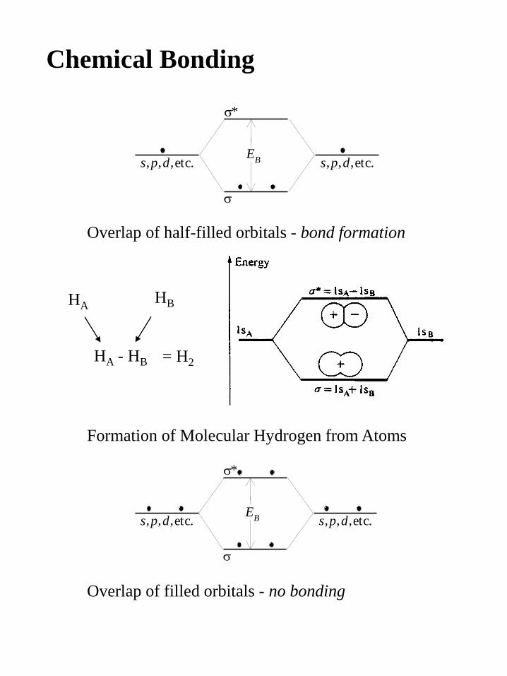
Chemical Bonding
Overlap of half-filled orbitals - bond formation
Overlap of filled orbitals - no bonding
HAHB
HA - HB = H2
Formation of Molecular Hydrogen from Atoms

Periodic Chart

Conduction Band
Valence Band
Egs3
p3
sp3
Si(separated atoms)
EV
EC
Si(atoms interact to form
tetrahedral bonding geometry )Si crystal
Crystal Bonding
sp3 bonding orbitals
sp3 antibonding orbitals
Silicon Crystal Bonding

Semiconductor Band Structures
Silicon
Germanium
Gallium Arsenide
Eg
NE
EN
V
V
C
C
EF
Conduction Band
Valence Band
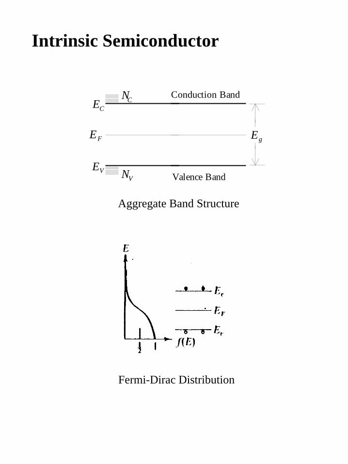
Intrinsic Semiconductor
Aggregate Band Structure
Fermi-Dirac Distribution

n-type Semiconductor
Aggregate Band Structure
Fermi-Dirac Distribution
Eg
NE
EN
V
V
C
C
Ei
EF
Conduction Band
Valence Band
Shallow Donor States
Donor Ionization

p-type Semiconductor
Aggregate Band Structure
Fermi-Dirac Distribution
Eg
NE
EN
V
V
C
C
Ei
EF
Conduction Band
Valence Band
Shallow Acceptor States
Acceptor Ionization
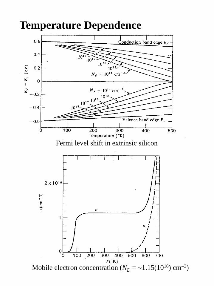
Temperature Dependence
Fermi level shift in extrinsic silicon
Mobile electron concentration (ND = 1.15(1016) cm3)

Carrier Mobility
Carrier drift velocity vs applied field in intrinsic silicon
No Field Field Present
Pictorial representation of carrier trajectory

Effect of Dopant Impurities
Effect of total dopant concentration on carrier mobility
Resistivity of bulk silicon as a function of net dopant concentration

The Seven Crystal Systems

Bravais Lattices

Diamond Cubic Lattice
a = lattice parameter; length of cubic unit cell edge
Silicon atoms have tetrahedral coordination in a
FCC (face centered cubic) Bravais lattice
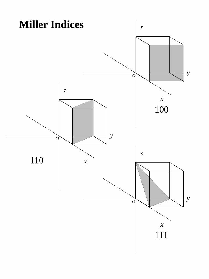
Miller Indices
O
z
y
x
O
z
y
x
O
z
y
x
100
110
111

Diamond Cubic Model
100
110
111
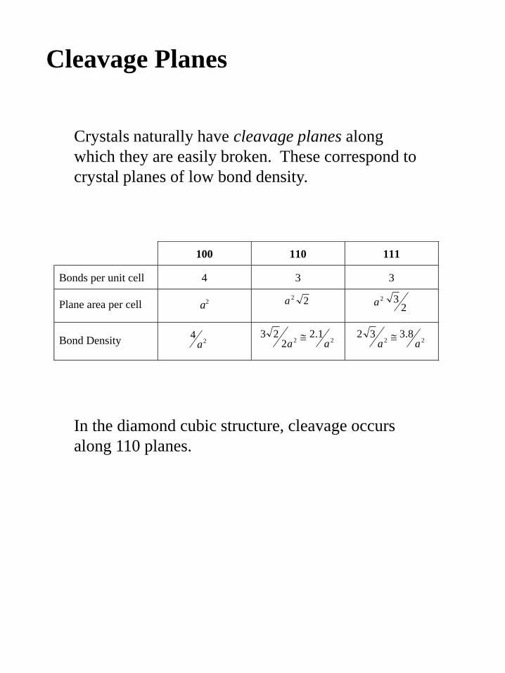
Cleavage Planes
Crystals naturally have cleavage planes along
which they are easily broken. These correspond to
crystal planes of low bond density.
100 110 111
Bonds per unit cell 4 3 3
Plane area per cell a2 22a2
32a
Bond Density 24
a22
1.22
23aa
228.332
aa
In the diamond cubic structure, cleavage occurs
along 110 planes.

[100] Orientation

[110] Orientation

[111] Orientation
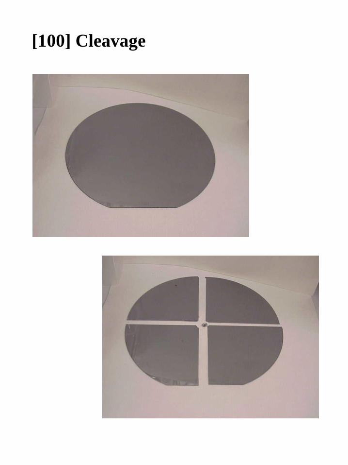
[100] Cleavage
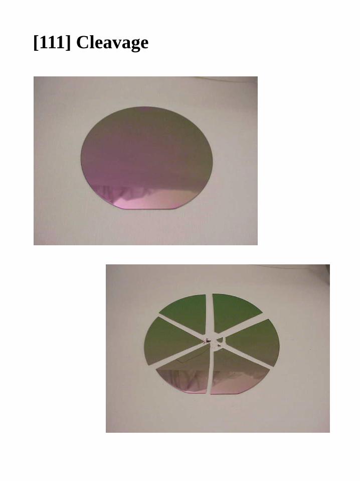
[111] Cleavage
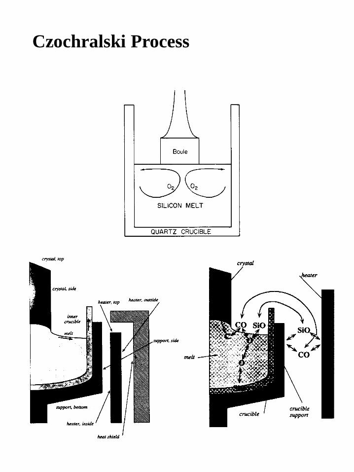
Czochralski Process
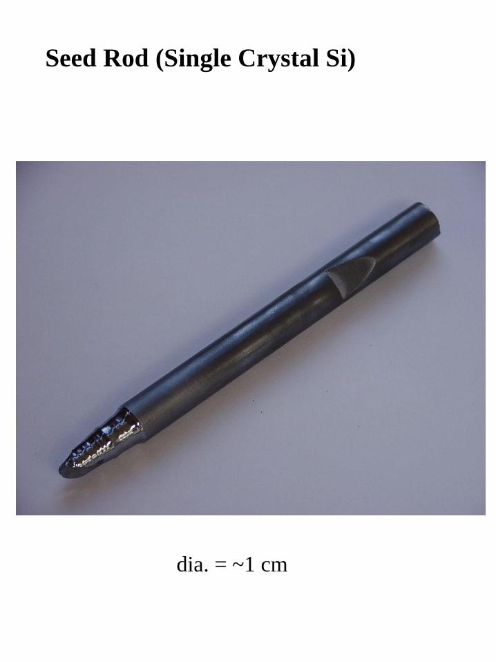
Seed Rod (Single Crystal Si)
dia. = ~1 cm
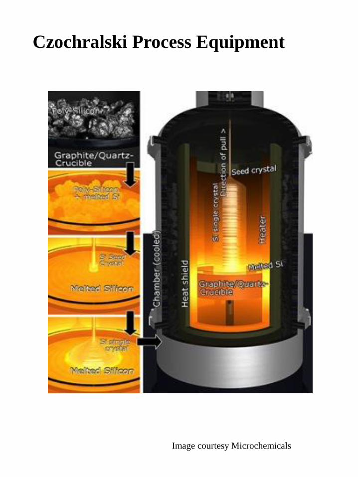
Czochralski Process Equipment
Image courtesy Microchemicals

Czochralski Factory and Boules

CZ Growth under Rapid Stirring
x=0
dxCs
Cl
Dopant K
B 0.72
P 0.32
As 0.27
Sb 0.020
Ga 0.0072
Al 0.0018
In 0.00036
Distribution Coefficients
0 .01
0 .1
1
10
0 0 .2 0 .4 0 .6 0 .8 1
Le ngth Fractio n
Do
pa
nt
Co
nce
ntr
ati
on
Ra
tio
0.5
0.9
0.3
0.2
0.1
0.050.01
CZ Dopant Profiles under Conditions of Rapid Stirring
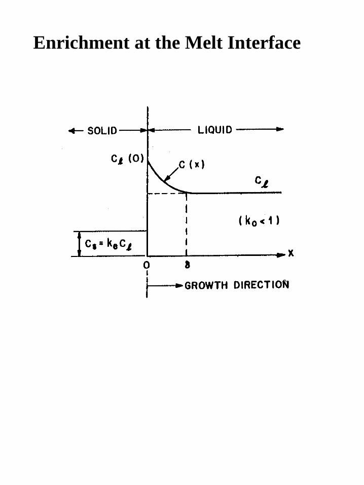
Enrichment at the Melt Interface

Si Ingot
Heater
Zone Refining
Ingot slowly passes through the needle’s eye heater so
that the molten zone is “swept” through the ingot from
one end to the other

Single Pass FZ Process
x=0 dx
L
x
C s C o
0.01
0.1
1
0 2 4 6 8 10
Zone Lengths
Do
pa
nt
Co
nce
ntr
ati
on R
ati
o
0.5
0.9
0.30.2
0.1
0.03
0.01

Multiple Pass FZ Process
0.01
0.1
1
0 2 4 6 8 10 12 14 16 18 20
Zone Lengths
Dopant
Co
nce
ntr
ati
on R
ati
o
0.50.9 0.3 0.2
0.1
0.03
0.01
Almost arbitrarily pure silicon
can be obtained by multiple
pass zone refining.

Vacancy (Schottky Defect)
“Dangling
Bonds”

Self-Interstital

Dislocations
Edge Dislocation
Screw Dislocation

Burgers Vector
Screw Dislocation
Edge Dislocation
Dislocations in Silicon
[100]
[111]

Stacking Faults
Intrinsic Stacking
Fault
Extrinsic Stacking
Fault
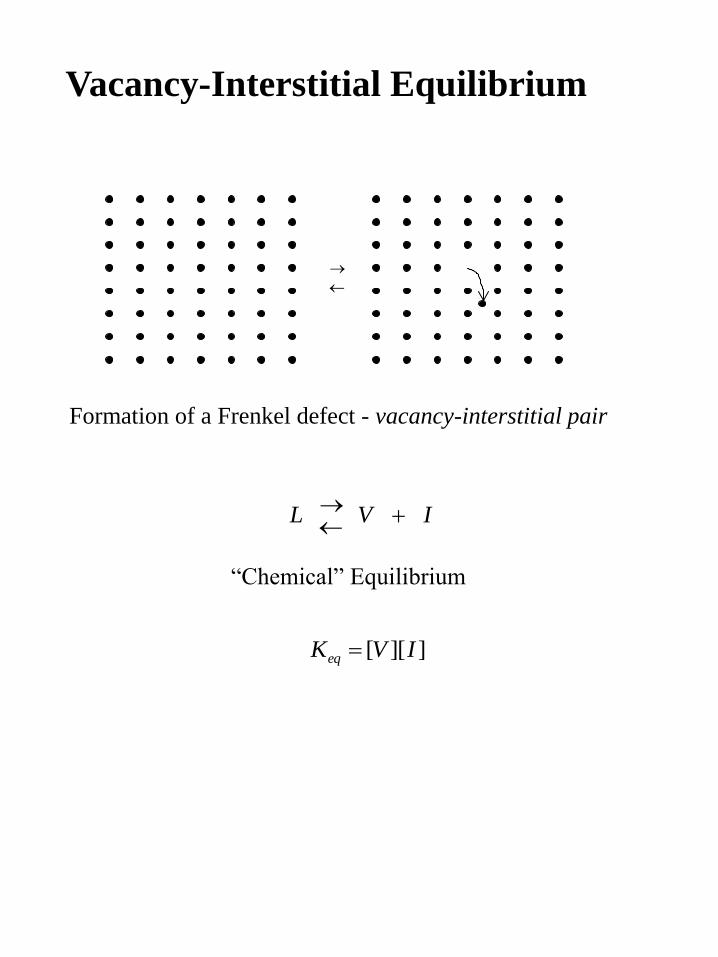
Vacancy-Interstitial Equilibrium
¬
®
Formation of a Frenkel defect - vacancy-interstitial pair
IVL +¨
“Chemical” Equilibrium
]][[ IVKeq =
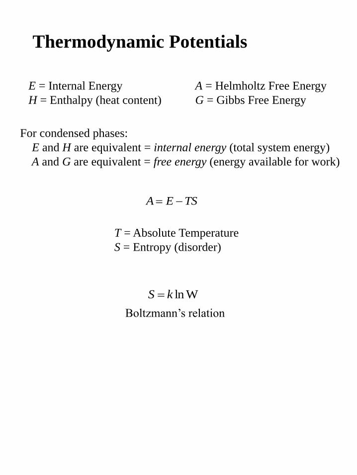
Thermodynamic Potentials
E = Internal Energy
H = Enthalpy (heat content)
A = Helmholtz Free Energy
G = Gibbs Free Energy
For condensed phases:
E and H are equivalent = internal energy (total system energy)
A and G are equivalent = free energy (energy available for work)
T = Absolute Temperature
S = Entropy (disorder)
A E TS=
WlnkS =
Boltzmann’s relation

Vacancy Formation
eV 3.2~ = vE
A M E T SMv v Mv=
MvMv kS Wln=
WMv
N
N M M=
!
( )! !
==
!)!(
!lnWln
MMN
NkkS MvMv
)ln()( MNkTMN
++= MMkTNNkTEMA vMv lnln

Additional Vacancy Formation
MA E kT M kT N MMv v = + ln ln( )
=
kT
ENM vexp
Vacancy “concentration”
Equilibrium Constant
Interstitial “concentration”
NN8
5=
=
=
kT
EN
kT
ENM ii exp
8
5exp
+=
kT
EENK iv
eq exp8
5 2
¬
®

Internal Gettering
OO
O
OO
O
OO
O
O
O
O
O2
O2O2
O2
O2denuded zone
Gettering removes harmful impurities from the
front side of the wafer rendering them electrically
innocuous.
oxygen nuclei
oxide precipitates(with dislocations and stacking faults)
High temperature anneal - denuded zone formation
Low temperature anneal - nucleation
Intermediate temperature anneal - precipitate growth
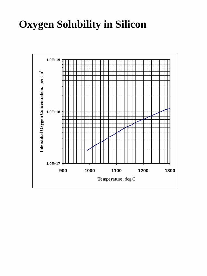
Oxygen Solubility in Silicon
1.0E+17
1.0E+18
1.0E+19
900 1000 1100 1200 1300
Temperature, deg C
Inte
rsti
tia
l O
xy
gen C
once
ntr
ati
on,
per
cm
3
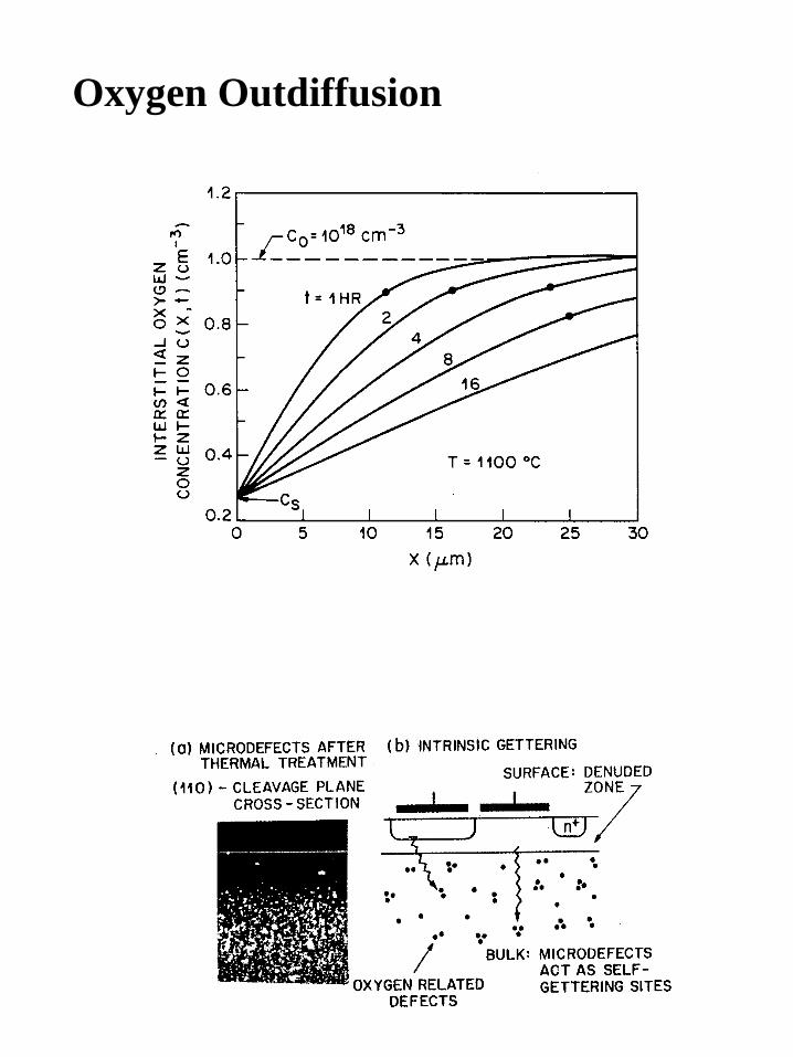
Oxygen Outdiffusion

Precipitate Free Energy
a) - Free energy of formation of a spherical precipitate as a function of
radius
b) - Saturated solid solution of B (e.g., interstitial oxygen) in A (e.g.,
silicon crystal)
c) - Nucleus formation
Ar
n E nT S g r= + +4
34
3
2
2 2
SiO SiO
++=
rgSnTEnrA
r84
22 SiOSiO
2

Critical Radius
a) – If critical radius exists, then a larger precipitate grows large
b) – If critical radius exists, then a smaller percipitate redissolves
gSnTEnrcrit
+
=
22 SiOSiO
2

Substrate Characterization by XRD
Constructive Interference Destructive Interference
Bragg pattern - [hk0], [h0l], or [0kl]

Wafer Finishing
Schematic of chemical mechanical polishing
Spindle
Pad
Table
Wafer Insert
Carrier
Capture Ring
Ingot slicing into raw wafers

Vapor-Liquid-Solid (VLS) Growth
substrate substrate
SiH4 SiH4
H2 H2 H2 H2
substrate
catalyst
Si nanowires grown by VLS (at IBM)
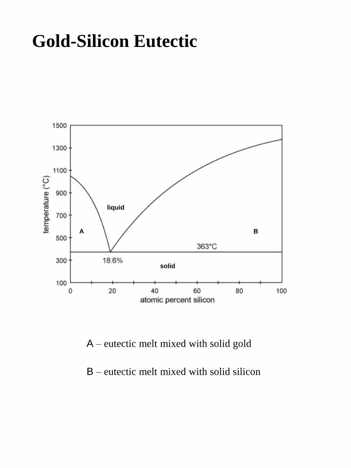
Gold-Silicon Eutectic
A B
liquid
solid
A – eutectic melt mixed with solid gold
B – eutectic melt mixed with solid silicon

Silicon Dioxide Network
Silanol
Non-bridging
oxygen
SiO4 tetrahedron
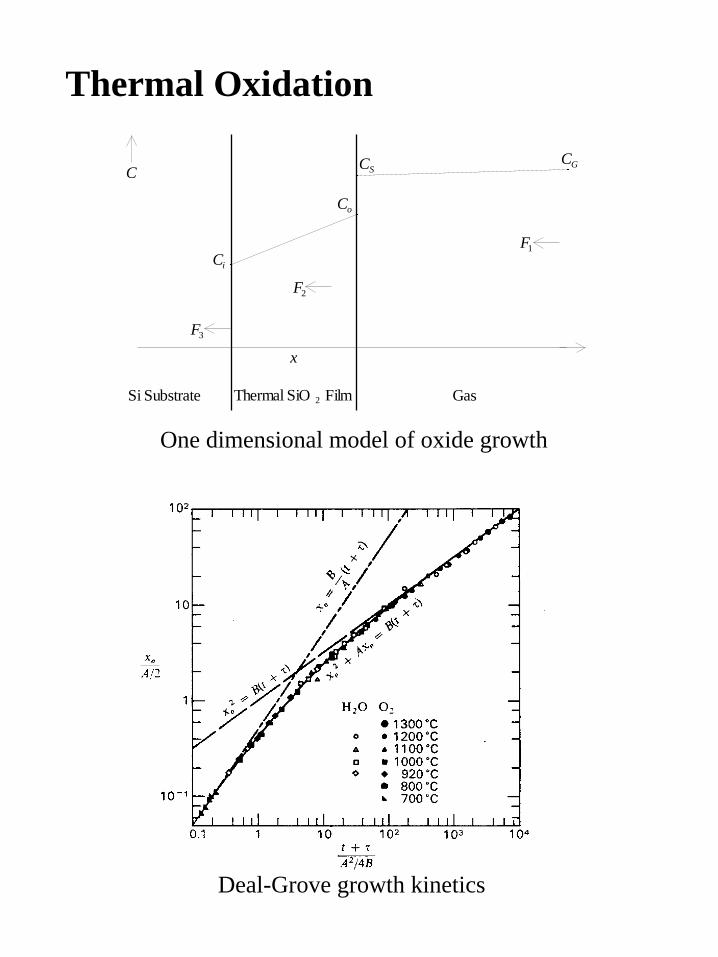
Thermal Oxidation
Thermal SiO 2 Film
F1
Si Substrate Gas
F2
F3
C
x
CGCS
Co
Ci
One dimensional model of oxide growth
Deal-Grove growth kinetics
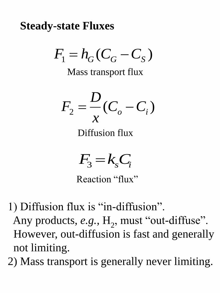
Steady-state Fluxes
)(1 SGG CChF =Mass transport flux
)(2 io CC
x
DF =
Diffusion flux
isCkF =3
Reaction “flux”
1) Diffusion flux is “in-diffusion”.
Any products, e.g., H2, must “out-diffuse”.
However, out-diffusion is fast and generally
not limiting.
2) Mass transport is generally never limiting.
S
o
C
CH =
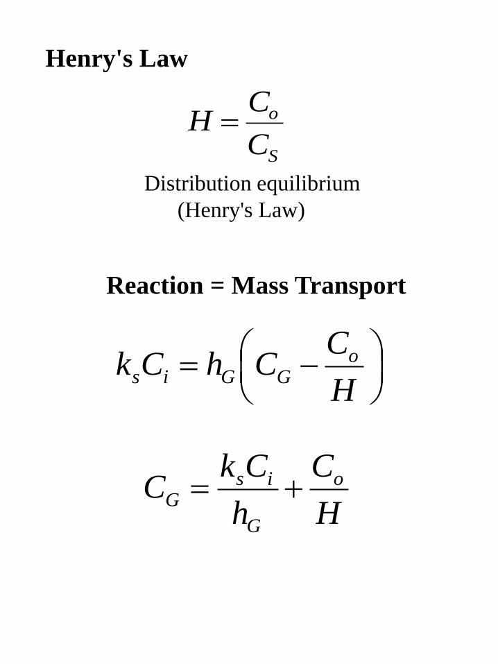
Henry's Law
Distribution equilibrium
(Henry's Law)
Reaction = Mass Transport
=
H
CChCk o
GGis
H
C
h
CkC o
G
isG +=
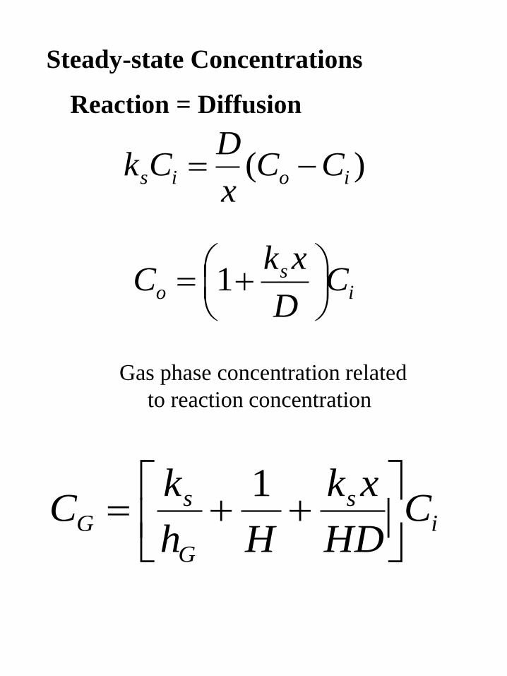
Steady-state Concentrations
Reaction = Diffusion
)( iois CC
x
DCk =
Gas phase concentration related
to reaction concentration
i
so C
D
xkC
+= 1
i
s
G
sG C
HD
xk
Hh
kC
++=
1

Deal-Grove Model
Relationship between thickness
and time:
+++
+=
Gs
G
Gs h
H
ktt
ND
HC
h
H
kDx
1)(
210
2
What if an oxide of thickenss, x0, is
already on the wafer?
Must calculate equivalent growth time
under desired conditions
1
3 1
++==
D
xk
h
HkHCk
dt
dxNF s
G
sGs
++= 0
2
00
12
2x
h
H
kDx
DHC
Nt
GsG

Deal-Grove Rate Constants
B/A => Linear Rate Constant
B => Parabolic Rate Constant
+=
Gs h
H
kDA
12
N
DHCB G2=
+
=
Gs
G
hHkN
C
A
B
11

Oxidation Kinetics
Reactant
Product
Transition
Ea
E
Energy‡
Process Coordinate
Process B/A for [100] B/A for [111] B
Dry Oxidation 1.03(103) kTe
00.2
1.73(103) kTe
00.2
0.214 kTe
23.1
Steam Oxidation 2.70(104) kTe
05.2
4.53(104) kTe
05.2
0.107 kTe
79.0
Note: Activation energies are in eV’s, B/A is in m/sec, B is in m2/sec
Rate constants for wet and dry oxidation on [100] and [111]
surfaces

Linear Rate Constant
Orientation dependence for [100] and [111] surfaces affects
only the “pre-exponential” factor and not the activation
energy
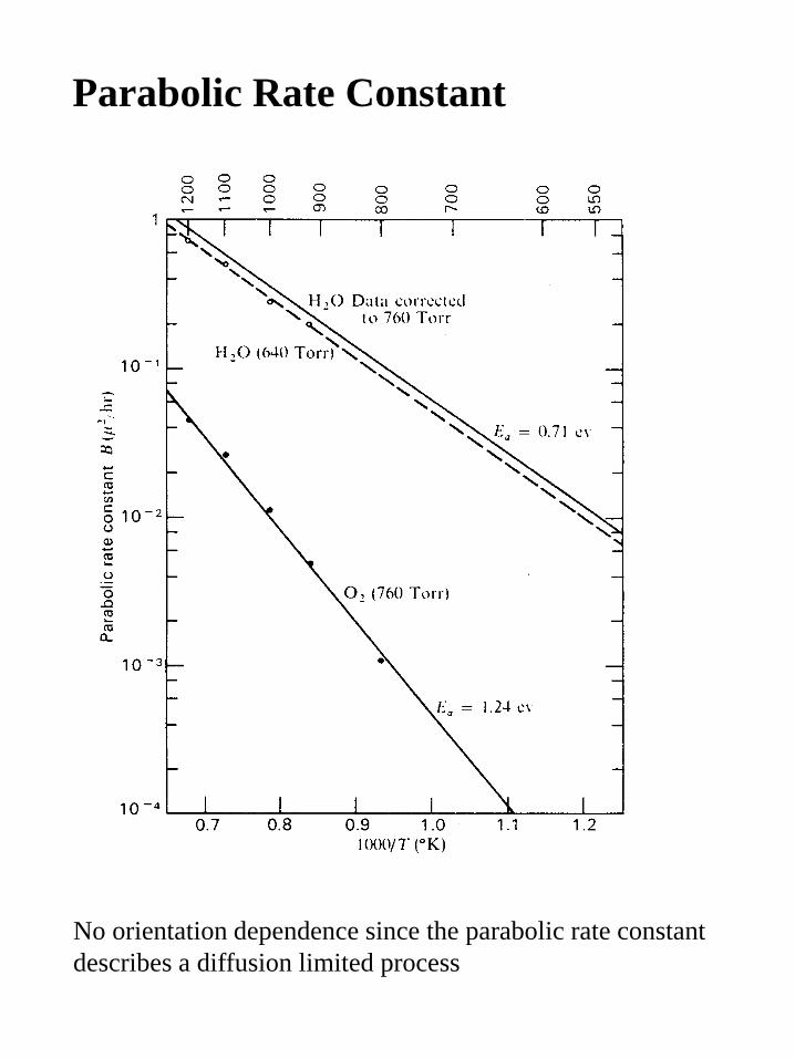
Parabolic Rate Constant
No orientation dependence since the parabolic rate constant
describes a diffusion limited process

Pressure Dependence
Oxidation rates scale linearly with oxidant pressure or partial
pressure
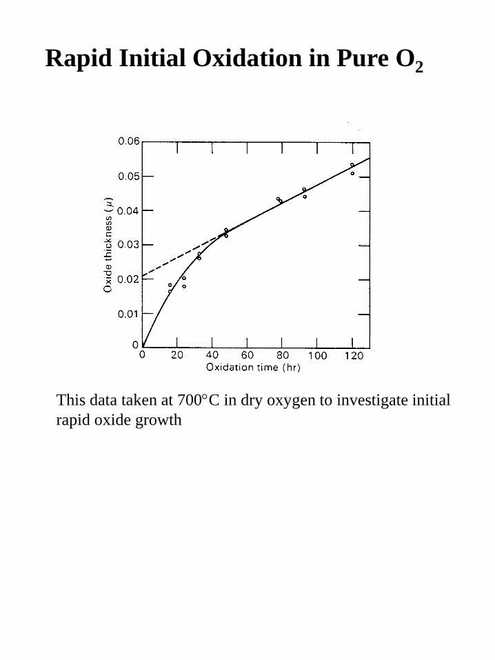
Rapid Initial Oxidation in Pure O2
This data taken at 700C in dry oxygen to investigate initial
rapid oxide growth
f1
f2
+
++
++
f2 f1
EF1
EF2
EF
Evac
y =
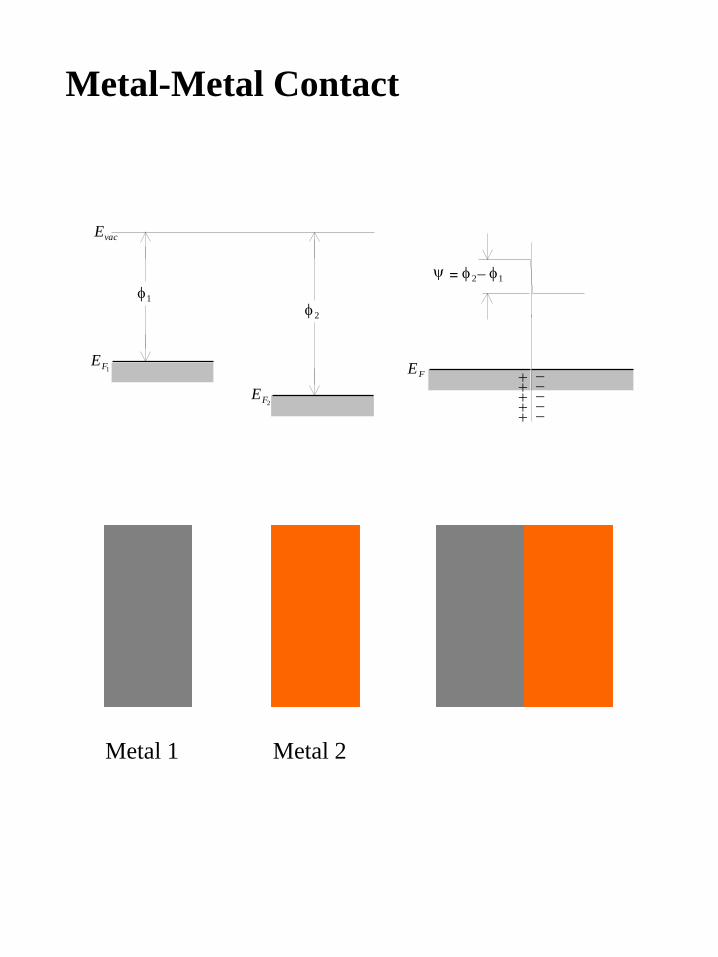
Metal-Metal Contact
Metal 1 Metal 2

Metal-Silicon Contact
EFSi
fM
+
++
++
EF
Evac
EFM
Ec
Ev
fSi
fMfSi
Metal Silicon

Effect of a Metal Contact on Silicon
Ec
Ev
jF
EF +
++
++
Ei
Ec
Ev
jF
EF +
++
++
Ei
Depletion (p-type) Inversion (p-type)
Ec
Ev
jF
EF +
++
++
Ei
Ec
Ev
jF
EF
Ei
Accumulation (n-type) Flat Band (n-type)
+
++
++
Ec
Ev
jF
Ei
EF
Depletion (n-type)

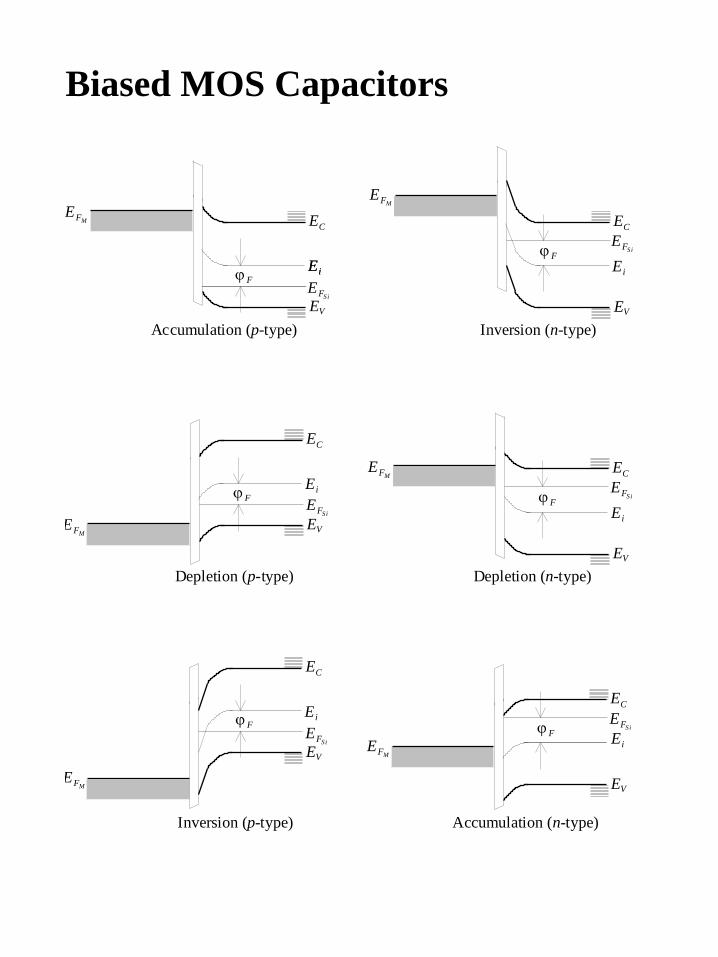
Metal-Oxide-Silicon Capacitor
EV
EC
EFSi
fM
+
++
EF
Evac
EFM
fSi
fMfSi
SiO2
f
Metal SiliconSilicon
Dioxide

MOS Capacitor on Doped Silicon
EV
EC
EFM
EijFEFSi
+
++
EV
EC
EFM
Ei
jF
EFSi
+
++
Depletion (p-type) Accumulation (n-type)
Vg
0 v
Schematic of biased MOS capacitor
EV
EC
jF
EiEi
EFSi
EFM
EV
EC
EFM
jF
Ei
EFSi
Accumulation (p-type) Inversion (n-type)
EV
EC
EFM
EijFEFSi
EV
ECEFM
jF
Ei
EFSi
Depletion (p-type) Depletion (n-type)
EV
EC
EFM
EijFEFSi
EV
EC
EFM
jFEi
EFSi
Inversion (p-type) Accumulation (n-type)
Biased MOS Capacitors

CV Response
n-type substrate
p-type substrate
0
1
2
3
4
5
6
7
8
9
10
-100 -50 0 50 100
Bias Voltage
Ca
pa
cit
an
ce
quasistatic
high frequency
depletion
approximation
0
1
2
3
4
5
6
7
8
9
10
-50 -40 -30 -20 -10 0 10 20 30 40 50
Bias Voltage
Ca
pa
cit
an
ce
quasistatic
high frequency
depletion
approximation
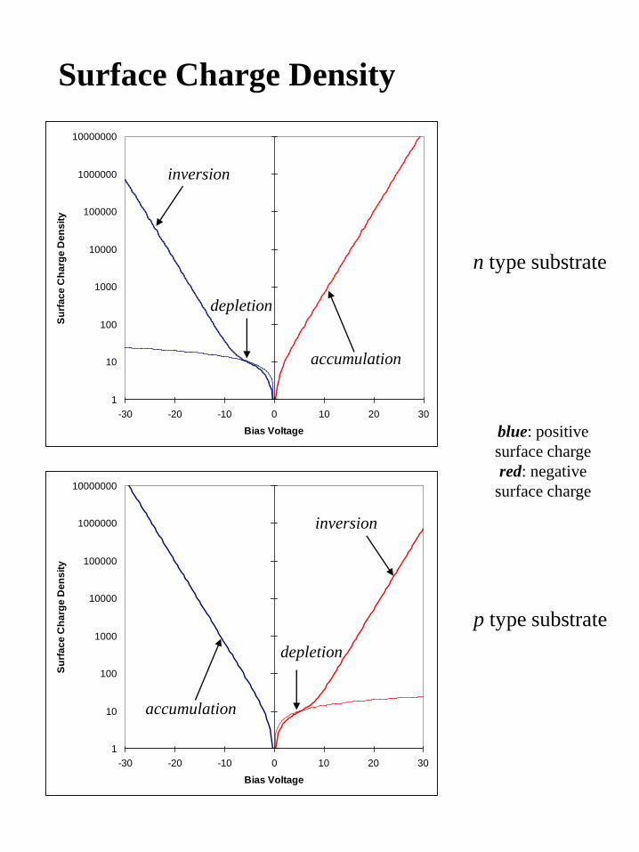
Surface Charge Density
1
10
100
1000
10000
100000
1000000
10000000
-30 -20 -10 0 10 20 30
Bias Voltage
Su
rfa
ce
Ch
arg
e D
en
sit
y
inversion
accumulation
depletion
1
10
100
1000
10000
100000
1000000
10000000
-30 -20 -10 0 10 20 30
Bias Voltage
Su
rfa
ce
Ch
arg
e D
en
sit
y
accumulation
depletion
inversion
n type substrate
p type substrate
blue: positive
surface charge
red: negative
surface charge
s
x
dx
d
=
j )(2
2
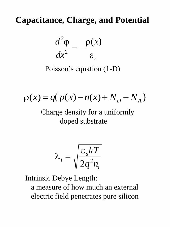
Capacitance, Charge, and Potential
Poisson’s equation (1-D)
Charge density for a uniformly
doped substrate
AD NNxnxpqx += )()()(
i
si
nq
kT22
=
Intrinsic Debye Length:
a measure of how much an external
electric field penetrates pure silicon

The Depletion Approximation
)()(
2
2
xNxNq
dx
dAD
s
=j
Carrier concentrations are negligible
in the depletion region
=
i
DA
DA
sd
n
NN
NNq
kTx ln
42
max
Maximum depletion width
DA
sD
NNq
kT
=
2
Extrinsic Debye Length:
a measure of how much an external
electric field penetrates doped silicon

CV vs Doping and Oxide Thickness
Substrate
Doping
Oxide
Thickness
p-type substrate0
1
2
3
4
5
6
7
8
9
10
-100 -50 0 50 100 150
Cap
acit
ance
(dim
ensi
on
less
lin
ear
scal
e)
0.1
1
10
100
1000
-150 -100 -50 0 50 100
Cap
acit
ance
(dim
ensi
on
less
logar
ithm
ic s
cale
)
Bias Voltage (dimensionless linear scale)
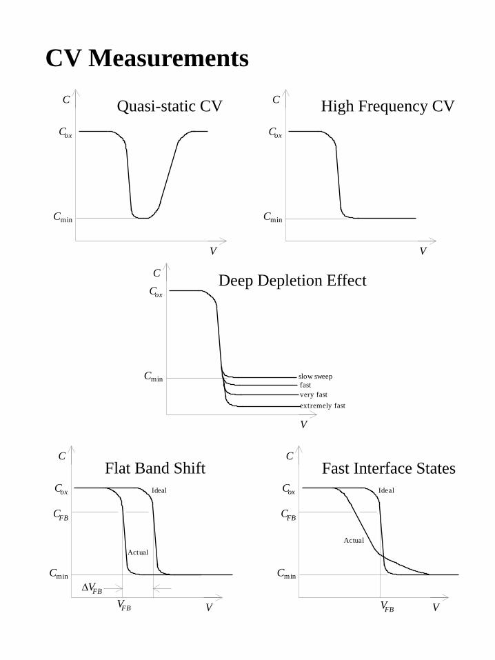
CV Measurements
V
C
Cmin
Cox
Quasi-static CV
V
C
Cmin
Cox
High Frequency CV
V
C
Cox
Cmin slow sweep
fast
very fast
extremely fast
Deep Depletion Effect
V
C
Cmin
Cox
FBC
VFB
VFB
Ideal
Actual
Flat Band Shift
V
C
Cmin
Cox
FBC
VFB
Ideal
Actual
Fast Interface States

Interface States
EV
EC
jF
EF
Ei
Interface states – caused by
broken symmetry at interface
Interface states – p-type depletion
Interface states – n-type depletion
EV
ECEFM
jF
Ei
EFSi
+++++
EV
EC
EFM
EijFEFSi

Interface State Density
Interface state density is always higher on [111] than [100]
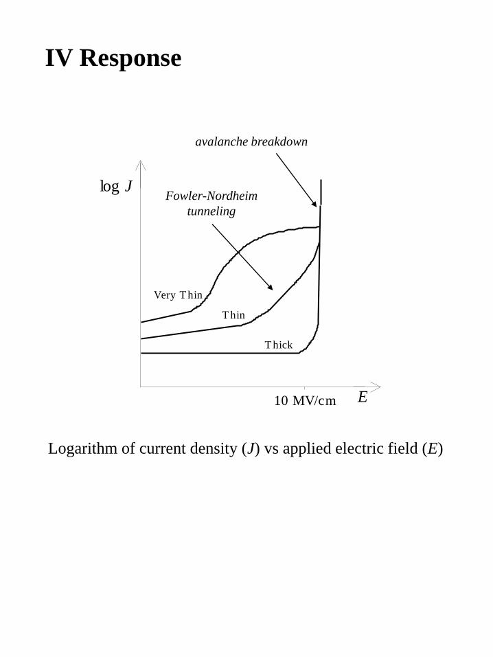
IV Response
log J
E10 MV/cm
T hick
T hin
Very T hin
Logarithm of current density (J) vs applied electric field (E)
Fowler-Nordheim
tunneling
avalanche breakdown

Conduction Mechanisms
=
E
EEAJ o
FN exp2 Fowler-Nordheim tunneling
f= kT
qEqEAJ
ox
BFP exp
Frenkel-Poole emission
f= kT
qEqTAJ
ox
B4
exp* 2
Schottky emission
kTEqEAJ aee = expOhmic (electronic)
conduction
kTEq
T
EAJ ai
i = exp Ionic conduction
3
2
8
9
o
ox
eox
x
VJ
=
Mobility limited breakdown
current
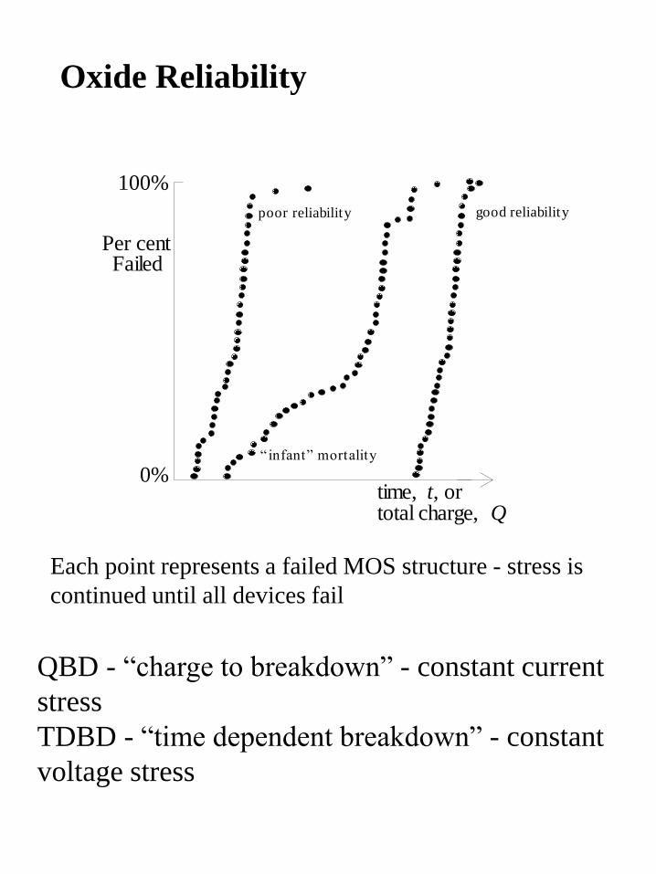
total charge, Qtime, t, or
100%
0%
FailedPer cent
good reliabilitypoor reliability
“ infant” mortality
Oxide Reliability
QBD - “charge to breakdown” - constant current
stress
TDBD - “time dependent breakdown” - constant
voltage stress
Each point represents a failed MOS structure - stress is
continued until all devices fail

Linear Transport Processes
Ohm’s Law of electrical conduction: j = E = E/
J = electric current
density, j
(units: A/cm2)
X = electric field,
E = V
(units: volt/cm)
V = electrical potential
L = conductivity,
= 1/
(units: mho/cm)
= resistivity ( cm)
Fourier’s Law of heat transport: q = T
J = heat flux, q
(units: W/cm2)
X = thermal force,
T
(units: K/cm)
T = temperature
L = thermal
conductivity,
(units: W/K cm)
Fick’s Law of diffusion: F = DC
J = material flux, F
(units: /sec cm2)
X = diffusion force,
C
(units: /cm4)
C = concentration
L = diffusivity, D
(units: cm2/sec)
Newton’s Law of viscous fluid flow: Fu = u
J = velocity flux, Fu
(units: /sec2 cm)
X = viscous force,
u
(units: /sec)
u = fluid velocity
L = viscosity,
(units: /sec cm)
J = LX
J = Flux, X = Force, L = Transport Coefficient

Diffusion
Diffusion in a rectangular bar of constant cross section
C
tD
C
x=
2
2
Fick’s Second Law
Dtxx
eDt
NtxC 4
20
2,
=
Instantaneous Source - Gaussian profile
Constant Source - error function profile
=
Dt
xxNtxC
2erfc
2, 00
A
x
x
F(x) xF(x )+

Instantaneous Source Profile
0
0.2
0.4
0.6
0.8
1
1.2
0 1 2 3 4 5
0.1
1.0
0 0.5 1 1.5 2
Linear scale
Log scale

Constant Source Profile
0
0.2
0.4
0.6
0.8
1
1.2
0 1 2 3 4 5
0.1
1.0
0 0.5 1 1.5 2
Linear scale
Log scale

Surface Probing
I
r
Substrate
Single probe injecting
current into a bulk
substrate
s ss
1 2 3 4
I I
Substrate
Four point probe
I
r
Substrate
T hin Film
xf
Single probe injecting
current into a
conductive thin film
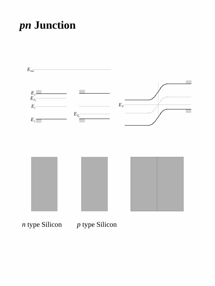
Ei
EFn
EFp
Evac
Ec
Ev
EF
pn Junction
n type Silicon p type Silicon

Junction Depth
0
0.2
0.4
0.6
0.8
1
1.2
0 1 2 3 4 5
0.01
0.10
1.00
0 0.5 1 1.5 2
xJ
xJ
red: background
doping
black: diffused
doping
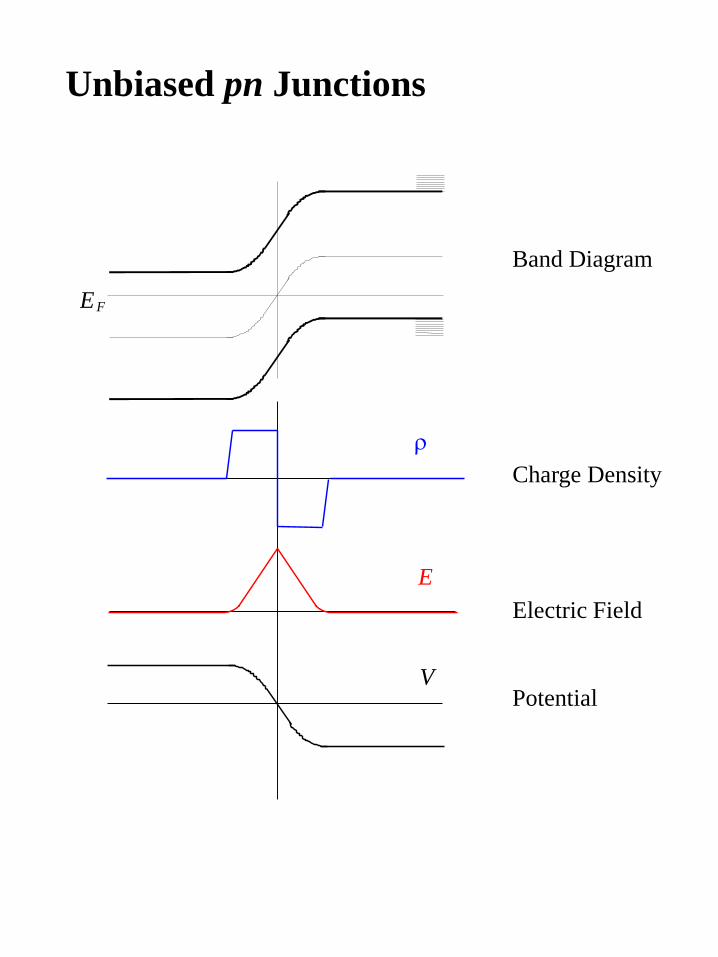
Unbiased pn Junctions
EF
E
V
Electric Field
Band Diagram
Charge Density
Potential

Biased pn Junctions
IV Characteristics
V
I
I0
V
2
1
C
Vpn
CV Characteristics
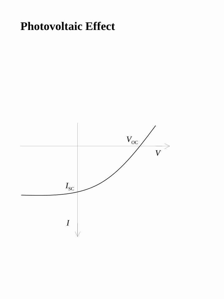
Photovoltaic Effect
V
I
ISC
VOC

Solar Cell
typical cross section
equivalent circuit
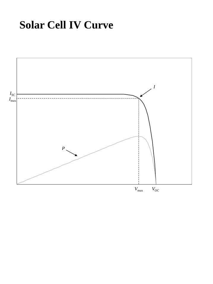
Solar Cell IV Curve
ISC
VOC
I
P
Vmax
Imax

Effect of Parasitics, Temperature, etc.
effect of RS effect of RSH
effect of I0 effect of n
effect of T
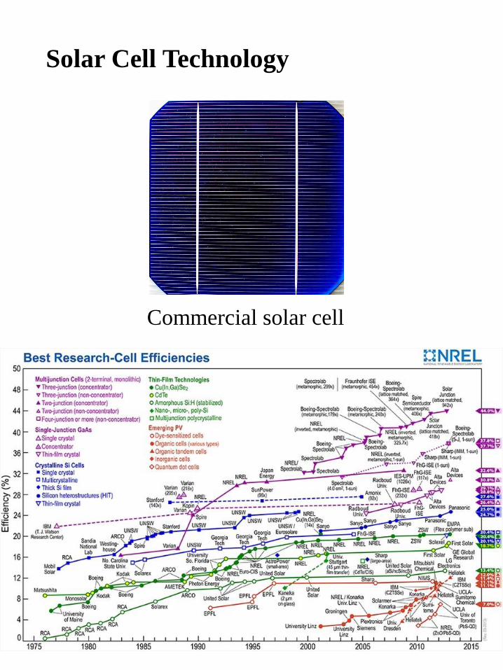
Solar Cell Technology
Commercial solar cell

LED IV Characteristics
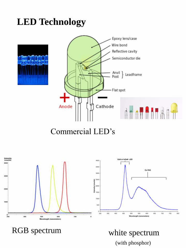
LED Technology
RGB spectrum
Commercial LED’s
white spectrum(with phosphor)
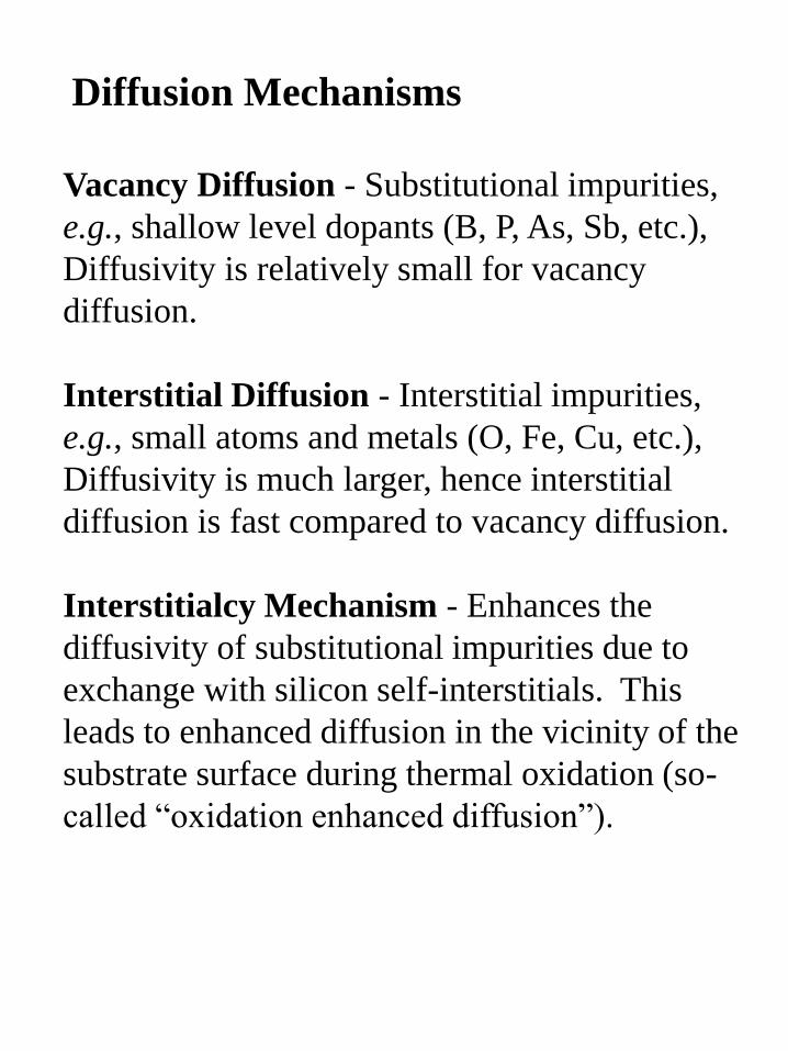
Diffusion Mechanisms
Vacancy Diffusion - Substitutional impurities,
e.g., shallow level dopants (B, P, As, Sb, etc.),
Diffusivity is relatively small for vacancy
diffusion.
Interstitial Diffusion - Interstitial impurities,
e.g., small atoms and metals (O, Fe, Cu, etc.),
Diffusivity is much larger, hence interstitial
diffusion is fast compared to vacancy diffusion.
Interstitialcy Mechanism - Enhances the
diffusivity of substitutional impurities due to
exchange with silicon self-interstitials. This
leads to enhanced diffusion in the vicinity of the
substrate surface during thermal oxidation (so-
called “oxidation enhanced diffusion”).

Defect-Carrier Equilibria
Vacancies interact with mobile carriers and
become charged. In this case, the concentrations
are governed by classical mass action equilibria.
V V h KV
Vpx
V x
®
¬
+
+ =
V V h KV
VpV
= + =
=
®
¬+ =
V V e KV
Vnx
V x
®
¬
+ +
+
+ =
V V e KV
VnV
+ ++ ++
++
+
®
¬+ =

Arrhenius Constants for Dopant Atoms
Atomic Species
I
Diffusion Mechanism rV
r
oID
(cm2/sec)
r
IQ
(eV)
Si xV
V
=V
+V
0.015
16
10
1180
3.89
4.54
5.1
5.09
As xV
V
0.066
12.0
3.44
4.05
B xV
+V
0.037
0.76
3.46
3.46
Ga xV
+V
0.374
28.5
3.39
3.92
P xV
V
=V
3.85
4.44
44.2
3.66
4.00
4.37
Sb xV
V
0.214
15.0
3.65
4.08
N xV 0.05 3.65
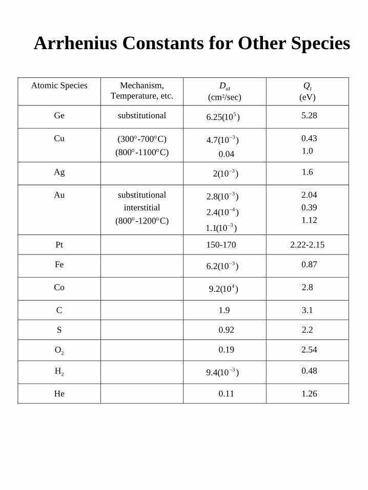
Arrhenius Constants for Other Species
Atomic Species Mechanism,
Temperature, etc.
DoI
(cm2/sec)
QI
(eV)
Ge substitutional )10(25.6 5 5.28
Cu (300-700C)
(800-1100C)
)10(7.4 3
0.04
0.43
1.0
Ag )10(2 3 1.6
Au substitutional
interstitial
(800-1200C)
)10(8.2 3
)10(4.2 4
)10(1.1 3
2.04
0.39
1.12
Pt 150-170 2.22-2.15
Fe )10(2.6 3 0.87
Co )10(2.9 4 2.8
C 1.9 3.1
S 0.92 2.2
O2 0.19 2.54
H2 )10(4.9 3 0.48
He 0.11 1.26

Solid Solubilities

Ion Implantation
Dopant species are ionized and accelerated by a
very high electric field. The ions then strike the
substrate at energies from 10 to 500 keV and
penetrate a short distance below the surface.
b
iv
|| v̂
^v̂
iv
i
s
q
sv
k̂ q
c
tangent plane(edge on)
Elementary “hard sphere” collision

Co-linear or “Centered” Collision
i
iv|| v̂
^v̂
iv
s
sv
k̂
tangent plane(edge on)b=0
c=
q=0
i
si
isi
si
sii v
mm
mvv
mm
mmv
+=
+
=
2 ;
Clearly, if mi<ms, then iv is negative. This means that light implanted ions tend to be
scattered back toward the surface. Conversely, if mi>ms, then iv is positive and heavy
ions tend to be scattered forward into the bulk. Obviously, if mi equals ms, then 0|| v̂v i
vanishes. In any case, recoiling silicon atoms are scattered deeper into the substrate.

Stopping Mechanisms
Nuclear Stopping - Direct interaction between
atomic nuclei; resembles an elementary two
body collision and causes most implant damage.
Electronic Stopping - Interaction between
atomic electron clouds; sort of a “viscous drag”
as in a liquid medium. Causes little damage.
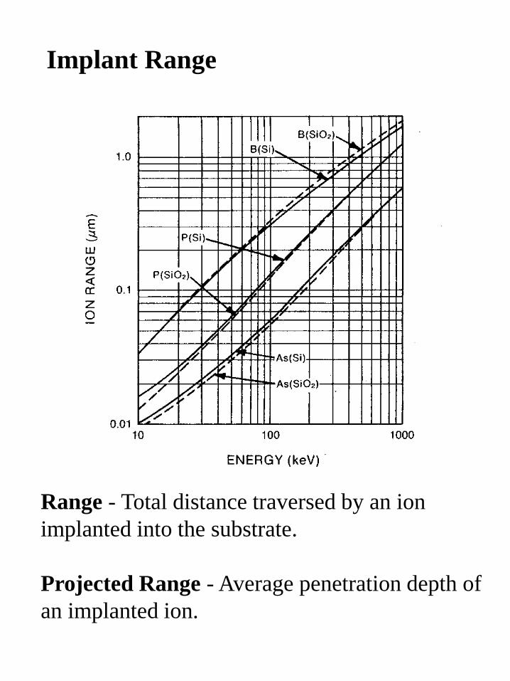
Implant Range
Range - Total distance traversed by an ion
implanted into the substrate.
Projected Range - Average penetration depth of
an implanted ion.

Implant Straggle
Projected Straggle - Variation in penetration
depth. (Corresponds to standard deviation if the
implanted profile is Gaussian.)

Channeling
Channeling is due to the crystal structure of the
substrate.

Implantation Process
For a light dose, damage is isolated. As dose is
increased, damage sites become more dense and
eventually merge to form an amorphous layer.
For high dose implants, the amorphous region
can reach all the way to the substrate surface.

Point-Contact Transistor

Bipolar Junction Transistor
n
n p
C B E

Junction FET
n
n p
S D G

MOSFET
p
n n
S D G
enhancement mode
p
n n
S D G
depletion mode

7 V
6 V
5 V
4 V
Enhancement Mode FET