microblaze debug module (mdm) v2.10 - xilinx
TRANSCRIPT

MicroBlaze Debug Module (MDM) v2.10.aProduct Guide
PG062 July 25, 2012

MicroBlaze Debug Module v2.10.a www.xilinx.com 2PG062 July 25, 2012
Table of Contents
SECTION I: SUMMARY
IP Facts
Chapter 1: OverviewFeature Summary. . . . . . . . . . . . . . . . . . . . . . . . . . . . . . . . . . . . . . . . . . . . . . . . . . . . . . . . . . . . . . . . . . 6Licensing and Ordering Information . . . . . . . . . . . . . . . . . . . . . . . . . . . . . . . . . . . . . . . . . . . . . . . . . . . 7
Chapter 2: Product SpecificationStandards Compliance . . . . . . . . . . . . . . . . . . . . . . . . . . . . . . . . . . . . . . . . . . . . . . . . . . . . . . . . . . . . . . 8Performance. . . . . . . . . . . . . . . . . . . . . . . . . . . . . . . . . . . . . . . . . . . . . . . . . . . . . . . . . . . . . . . . . . . . . . 8Resource Utilization. . . . . . . . . . . . . . . . . . . . . . . . . . . . . . . . . . . . . . . . . . . . . . . . . . . . . . . . . . . . . . . . 8Port Descriptions . . . . . . . . . . . . . . . . . . . . . . . . . . . . . . . . . . . . . . . . . . . . . . . . . . . . . . . . . . . . . . . . . . 9Register Space . . . . . . . . . . . . . . . . . . . . . . . . . . . . . . . . . . . . . . . . . . . . . . . . . . . . . . . . . . . . . . . . . . . 13
Chapter 3: Designing with the CoreGeneral Design Guidelines . . . . . . . . . . . . . . . . . . . . . . . . . . . . . . . . . . . . . . . . . . . . . . . . . . . . . . . . . 14Clocking. . . . . . . . . . . . . . . . . . . . . . . . . . . . . . . . . . . . . . . . . . . . . . . . . . . . . . . . . . . . . . . . . . . . . . . . . 14Resets . . . . . . . . . . . . . . . . . . . . . . . . . . . . . . . . . . . . . . . . . . . . . . . . . . . . . . . . . . . . . . . . . . . . . . . . . . 15Protocol Description . . . . . . . . . . . . . . . . . . . . . . . . . . . . . . . . . . . . . . . . . . . . . . . . . . . . . . . . . . . . . . 15
SECTION II: VIVADO DESIGN SUITE
Chapter 4: Customizing and Generating the CoreGUI . . . . . . . . . . . . . . . . . . . . . . . . . . . . . . . . . . . . . . . . . . . . . . . . . . . . . . . . . . . . . . . . . . . . . . . . . . . . 17Parameter Values. . . . . . . . . . . . . . . . . . . . . . . . . . . . . . . . . . . . . . . . . . . . . . . . . . . . . . . . . . . . . . . . . 18Output Generation. . . . . . . . . . . . . . . . . . . . . . . . . . . . . . . . . . . . . . . . . . . . . . . . . . . . . . . . . . . . . . . . 19
Chapter 5: Constraining the CoreRequired Constraints . . . . . . . . . . . . . . . . . . . . . . . . . . . . . . . . . . . . . . . . . . . . . . . . . . . . . . . . . . . . . . 20Device, Package, and Speed Grade Selections. . . . . . . . . . . . . . . . . . . . . . . . . . . . . . . . . . . . . . . . . . 20

MicroBlaze Debug Module v2.10.a www.xilinx.com 3PG062 July 25, 2012
Clock Frequencies . . . . . . . . . . . . . . . . . . . . . . . . . . . . . . . . . . . . . . . . . . . . . . . . . . . . . . . . . . . . . . . . 20Clock Management . . . . . . . . . . . . . . . . . . . . . . . . . . . . . . . . . . . . . . . . . . . . . . . . . . . . . . . . . . . . . . . 20Clock Placement. . . . . . . . . . . . . . . . . . . . . . . . . . . . . . . . . . . . . . . . . . . . . . . . . . . . . . . . . . . . . . . . . . 20Banking . . . . . . . . . . . . . . . . . . . . . . . . . . . . . . . . . . . . . . . . . . . . . . . . . . . . . . . . . . . . . . . . . . . . . . . . . 21Transceiver Placement . . . . . . . . . . . . . . . . . . . . . . . . . . . . . . . . . . . . . . . . . . . . . . . . . . . . . . . . . . . . 21I/O Standard and Placement. . . . . . . . . . . . . . . . . . . . . . . . . . . . . . . . . . . . . . . . . . . . . . . . . . . . . . . . 21
SECTION III: ISE DESIGN SUITE
Chapter 6: Customizing and Generating the CoreGUI . . . . . . . . . . . . . . . . . . . . . . . . . . . . . . . . . . . . . . . . . . . . . . . . . . . . . . . . . . . . . . . . . . . . . . . . . . . . 23Parameter Values. . . . . . . . . . . . . . . . . . . . . . . . . . . . . . . . . . . . . . . . . . . . . . . . . . . . . . . . . . . . . . . . . 24Parameter-Port Dependencies . . . . . . . . . . . . . . . . . . . . . . . . . . . . . . . . . . . . . . . . . . . . . . . . . . . . . . 26
Chapter 7: Constraining the Core
SECTION IV: APPENDICES
Appendix A: Application Software DevelopmentDevice Drivers . . . . . . . . . . . . . . . . . . . . . . . . . . . . . . . . . . . . . . . . . . . . . . . . . . . . . . . . . . . . . . . . . . . 29
Appendix B: Additional ResourcesXilinx Resources . . . . . . . . . . . . . . . . . . . . . . . . . . . . . . . . . . . . . . . . . . . . . . . . . . . . . . . . . . . . . . . . . . 30Solution Centers. . . . . . . . . . . . . . . . . . . . . . . . . . . . . . . . . . . . . . . . . . . . . . . . . . . . . . . . . . . . . . . . . . 30References . . . . . . . . . . . . . . . . . . . . . . . . . . . . . . . . . . . . . . . . . . . . . . . . . . . . . . . . . . . . . . . . . . . . . . 30Technical Support . . . . . . . . . . . . . . . . . . . . . . . . . . . . . . . . . . . . . . . . . . . . . . . . . . . . . . . . . . . . . . . . 31Revision History . . . . . . . . . . . . . . . . . . . . . . . . . . . . . . . . . . . . . . . . . . . . . . . . . . . . . . . . . . . . . . . . . . 31Notice of Disclaimer. . . . . . . . . . . . . . . . . . . . . . . . . . . . . . . . . . . . . . . . . . . . . . . . . . . . . . . . . . . . . . . 31
MicroBlaze Debug Module v2.10.a www.xilinx.com 4PG062 July 25, 2012
SECTION I: SUMMARY
IP Facts
Overview
Product Specification
Designing with the Core

MicroBlaze Debug Module v2.10.a www.xilinx.com 5PG062 July 25, 2012 Product Specification
IntroductionThis document provides the design specif ication for the MicroBlaze™ Debug Module (MDM) which enables JTAG-based debugging of one or more MicroBlaze processors.
Features• Support for JTAG-based software debug
tools
• Support for debugging up to 32 MicroBlaze processors (version 7 and higher)
• Support for synchronized control of multiple MicroBlaze processors
• Support for a JTAG-based UART with a configurable AXI4-Lite or PLBv46 interface
• Based on Boundary Scan (BSCAN) logic in Xilinx® FPGAs
• Supports connection to the ChipScope™ Pro ICON core through BSCAN signals for Spartan-3 FPGAs
IP Facts
LogiCORE IP Facts Table
Core Specifics
Supported Device Family(1)
Zynq™-7000(2), Virtex-7, Kintex™-7, Artix™-7,Virtex-6, Virtex-5, Spartan-6, Virtex®-4,
Spartan®-3
Supported User Interfaces AXI4-Lite(3), PLBv46
Resources See Table 2-1
Provided with Core
Design FilesISE: VHDL
Vivado: RTL
Example Design Not Provided
Test Bench Not Provided
Constraints File Not Provided
Simulation Model VHDL Behavioral
Supported S/W Driver(4) Standalone and Linux
Tested Design Tools(5)
Design Entry Tools
Xilinx Platform Studio (XPS)Vivado Design Suite(6)
Simulation Mentor Graphics Modelsim
Synthesis ToolsXilinx Synthesis Technology (XST)
Vivado Synthesis
SupportProvided by Xilinx @ www.xilinx.com/support
Notes: 1. For a complete list of supported derivative devices, see the
Embedded Edition Derivative Device Support.2. Supported in ISE Design Suite implementations only.3. The AXI4-Lite interface is not supported by Spartan-3,
Virtex-4, and Virtex-5.4. Standalone driver details can be found in the EDK or SDK
directory (<install_directory>/doc/usenglish/xilinx_drivers.htm). Linux OS and driver support information is available from //wiki.xilinx.com.
5. For the supported versions of the tools, see the Xilinx Design Tools: Release Notes Guide.
6. Supports only 7 series devices.

MicroBlaze Debug Module v2.10.a www.xilinx.com 6PG062 July 25, 2012
Chapter 1
OverviewThe block diagram of the MicroBlaze™ Debug Module is shown in Figure 1-1.
Feature SummaryThe MicroBlaze Debug Module (MDM):
• Enables JTAG-based debugging of one or more MicroBlaze processors.
• Instantiates one BSCAN primitive, or allows an external BSCAN to be used. In devices that contain more than one BSCAN primitive, MDM uses the USER2 BSCAN by default.
• Includes a UART with a configurable slave bus interface which can be configured for either an AXI4-Lite interconnect or a PLBv46 bus. The UART TX and RX signals are transmitted over the FPGA JTAG port to and from the Xilinx Microprocessor Debug (XMD) tool. The UART behaves in a manner similar to the LogiCORE™ IP AXI (UART) Lite core.
X-Ref Target - Figure 1-1
Figure 1-1: Microblaze Debug Module (MDM) Block Diagram
MDM
XILINXBSCAN
MDMControl/Status
MicroBlazeDebugControl
UARTControl
MicroBlazeTrace CoreInterface
MBDEBUG_0
MBDEBUG_31
...
S_AXI/SPLB
Interrupt
XMTCExternalBSCAN

MicroBlaze Debug Module v2.10.a www.xilinx.com 7PG062 July 25, 2012
Licensing and Ordering Information
Licensing and Ordering InformationThis Xilinx LogiCORE IP module is provided at no additional cost with the Xilinx Vivado™ Design Suite and ISE® Design Suite Embedded Edition tools under the terms of the Xilinx End User License.
Information about this and other Xilinx LogiCORE IP modules is available at the Xilinx Intellectual Property page. For information on pricing and availability of other Xilinx LogiCORE IP modules and tools, contact your local Xilinx sales representative.

MicroBlaze Debug Module v2.10.a www.xilinx.com 8PG062 July 25, 2012 Product Specification
Chapter 2
Product Specification
Standards ComplianceThe MDM adheres to the AMBA® AXI4 Interface standard (see ARM® AMBA AXI Protocol Specification, Version 2.0 ARM IHI 002C).
The MDM implements a Processor Local Bus slave interface (see IBM 128-Bit Processor Local Bus Architectural Specification (v4.6)).
PerformanceThe frequency and latency of the MicroBlaze™ Debug Module are optimized for use together with MicroBlaze. This means that the frequency targets are aligned to MicroBlaze targets.
Resource UtilizationBecause the MDM is a module that is used with other design elements in the FPGA, the utilization and timing numbers reported in this section are estimates, and the actual utilization of FPGA resources and timing of the MDM design can vary from the results reported in Table 2-1.
Table 2-1: Performance and Resource Utilization on Virtex®-6 (xc6vlx240t-ff1156-1)
Parameter Values (other parameters have default values) Device Resources
C_USE_UART C_MB_DBG_PORTS Flip-Flops LUTs
0 1 69 49
0 2 71 60
0 4 73 78
0 32 125 336
1 1 131 140

MicroBlaze Debug Module v2.10.a www.xilinx.com 9PG062 July 25, 2012 Product Specification
Port Descriptions
Port DescriptionsThe I/O signals for the MicroBlaze Debug Module (MDM) are listed and described in Table 2-2.
Table 2-2: MDM I/O Signals
Signal Name Interface I/O InitialState Description
System Signals
Interrupt O 0 Interrupt from UART
Debug_SYS_Rst O 0 Debug system reset
Ext_BRK O 0 External break
Ext_NM_BRK O 0 External non-maskable break
PLB Interface Signals
SPLB_Clk SPLB I - PLB clock
SPLB_Rst SPLB I - PLB reset
PLB_ABus[0:31] SPLB I - PLB address bus
PLB_UABus[0:31] SPLB I - PLB upper address bus
PLB_PAValid SPLB I - PLB primary address valid
PLB_SAValid SPLB I - PLB secondary address valid
PLB_rdPrim SPLB I - PLB secondary to primary read request indicator
PLB_wrPrim SPLB I - PLB secondary to primary write request indicator
PLB_MasterID[0:C_SPLB_MID_WIDTH-1] SPLB I - PLB current master identif ier
PLB_busLock SPLB I - PLB bus lock
PLB_abort SPLB I - PLB abort
PLB_RNW SPLB I - PLB read not write
PLB_BE[0:C_SPLB_DWIDTH/8 - 1] SPLB I - PLB byte enables
PLB_MSize[0:1] SPLB I - PLB data bus width indicator
PLB_size[0:3] SPLB I - PLB size of requested transfer
PLB_type[0"2] SPLB I - PLB transfer type
PLB_lockErr SPLB I - PLB lock error
PLB_wrDBus[0:C_SPLB_DWIDTH-1] SPLB I - PLB write data bus
PLB_wrBurst SPLB I - PLB burst write transfer
PLB_rdBurst SPLB I - PLB burst read transfer
PLB_wrPendReq SPLB I - PLB pending bus write request
PLB_rdPendReq SPLB I - PLB pending bus read request

MicroBlaze Debug Module v2.10.a www.xilinx.com 10PG062 July 25, 2012 Product Specification
Port Descriptions
PLB_wrPendPri[0:1] SPLB I - PLB pending write request priority
PLB_rdPendPri[0:1] SPLB I - PLB pending read request priority
PLB_reqPri[0:1] SPLB I - PLB current request priority
PLB_TAttribute[0:15] SPLB I - PLB transfer attribute
Sl_addrAck SPLB O - Slave address acknowledge
Sl_SSize[0:1] SPLB O - Slave data bus size
Sl_wait SPLB O - Slave wait
Sl_rearbitrate SPLB O - Slave bus re-arbitrate
Sl_wrDAck SPLB O - Slave write data acknowledge
Sl_wrComp SPLB O - Slave write transfer complete
Sl_wrBTerm SPLB O - Slave terminate write burst transfer
Sl_rdDBus[0:C_SPLB_DWIDTH -1] SPLB O - Slave read data bus
Sl_rdWdAddr[0:3] SPLB O - Slave read word address
Sl_rdAck SPLB O - Slave read data acknowledge
Sl_rdComp SPLB O - Slave read transfer complete
Sl_rdBTerm SPLB O - Slave terminate read burst transfer
Sl_MBusy [0:C_SPLB_NUM_MASTERS-1] SPLB O - Slave busy
Sl_MWrErr[0:C_SPLB_NUM_MASTERS-1] SPLB O - Slave write error
Sl_MrdErr[0:C_SPLB_NUM_MASTERS-1] SPLB O - Slave read error
Sl_MIRQ[0:C_SPLB_NUM_MASTERS-1]
SPLB O - Master interrupt request
Table 2-2: MDM I/O Signals (Cont’d)
Signal Name Interface I/O InitialState Description

MicroBlaze Debug Module v2.10.a www.xilinx.com 11PG062 July 25, 2012 Product Specification
Port Descriptions
AXI4-Lite Interface Signals
S_AXI_ACLK S_AXI I - AXI Clock
S_AXI_ARESETN S_AXI I - AXI Reset, active low
S_AXI_AWADDR[C_S_AXI_ADDR_WIDTH-1:0] S_AXI I - Write Address
S_AXI_AWVALID S_AXI I - Write Address Valid
S_AXI_AWREADY S_AXI O 0 Write Address Ready
S_AXI_AWDATA[C_S_AXI_DATA_WIDTH-1:0] S_AXI I - Write Data
S_AXI_AWSTB[C_S_AXI_DATA_WIDTH/8-1:0] S_AXI I - Write Strobes
S_AXI_WVALID S_AXI I - Write Valid
S_AXI_WREADY S_AXI O 0 Write Ready
S_AXI_BRESP[1:0] S_AXI O 0 Write Response
S_AXI_BVALID S_AXI O 0 Write Response Valid
S_AXI_BREADY S_AXI I - Write Response Ready
S_AXI_ARADDR[C_S_AXI_ADDR_WIDTH-1:0] S_AXI I - Read Address
S_AXI_ARVALID S_AXI I - Read Address Valid
S_AXI_ARREADY S_AXI O 0 Read Address Ready
S_AXI_RRESP[1:0] S_AXI O 0 Read Response
S_AXI_RVALID S_AXI O 0 Read Valid
S_AXI_RREADY S_AXI I - Read Ready
MicroBlaze Debug Interface Signals
Dbg_Clk_n MBDEBUG_n O 0 MicroBlaze Debug Clock
Dbg_TDI_n MBDEBUG_n O 0 MicroBlaze Debug TDI
Dbg_TDO_n MBDEBUG_n I - MicroBlaze Debug TDO
Dbg_Reg_En_n MBDEBUG_n O 0 MicroBlaze Debug Register Enable
Dbg_Capture_n MBDEBUG_n O 0 MicroBlaze Debug Capture
Dbg_Shift_n MBDEBUG_n O 0 MicroBlaze Debug Shift
Dbg_Update_n MBDEBUG_n O 0 MicroBlaze Debug Update
Dbg_Rst_n MBDEBUG_n O 0 MicroBlaze Debug Reset
MicroBlaze Trace Core Interface Signals
Ext_JTAG_DRCK XMTC O 0 Connection to MicroBlaze Trace Core
Ext_JTAG_RESET XMTC O 0 Connection to MicroBlaze Trace Core
Ext_JTAG_SEL XMTC O 0 Connection to MicroBlaze Trace Core
Table 2-2: MDM I/O Signals (Cont’d)
Signal Name Interface I/O InitialState Description

MicroBlaze Debug Module v2.10.a www.xilinx.com 12PG062 July 25, 2012 Product Specification
Port Descriptions
Ext_JTAG_CAPTURE XMTC O 0 Connection to MicroBlaze Trace Core
Ext_JTAG_SHIFT XMTC O 0 Connection to MicroBlaze Trace Core
Ext_JTAG_UPDATE XMTC O 0 Connection to MicroBlaze Trace Core
Ext_JTAG_TDI XMTC O 0 Connection to MicroBlaze Trace Core
Ext_JTAG_TDO XMTC I - Connection to MicroBlaze Trace Core
Chipscope ICON Interface Signals
bscan_tdi ICON O 0 Connection to Chipscope ICON core
bscan_reset ICON O 0 Connection to Chipscope ICON core
bscan_shift ICON O 0 Connection to Chipscope ICON core
bscan_update ICON O 0 Connection to Chipscope ICON core
bscan_capture ICON O 0 Connection to Chipscope ICON core
bscan_sel1 ICON O 0 Connection to Chipscope ICON core
bscan_drck1 ICON O 0 Connection to Chipscope ICON core
bscan_tdo1 ICON I - Connection to Chipscope ICON core
External BSCAN Interface Signals
bscan_tdi BSCAN I - Connection to external BSCAN
bscan_reset BSCAN I - Connection to external BSCAN
bscan_shift BSCAN I - Connection to external BSCAN
bscan_update BSCAN I - Connection to external BSCAN
bscan_capture BSCAN I - Connection to external BSCAN
bscan_sel BSCAN I - Connection to external BSCAN
bscan_drck BSCAN I - Connection to external BSCAN
bscan_tdo BSCAN O 0 Connection to external BSCAN
Table 2-2: MDM I/O Signals (Cont’d)
Signal Name Interface I/O InitialState Description
MicroBlaze Debug Module v2.10.a www.xilinx.com 13PG062 July 25, 2012 Product Specification
Register Space
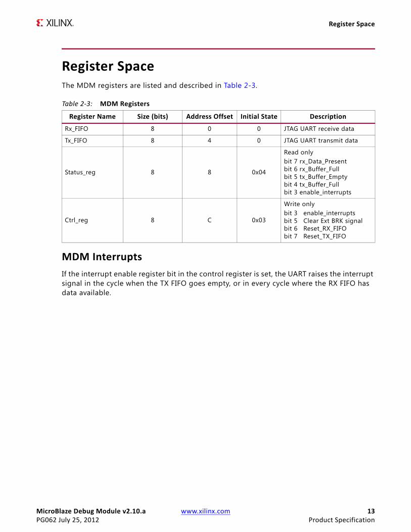
Register SpaceThe MDM registers are listed and described in Table 2-3.
MDM InterruptsIf the interrupt enable register bit in the control register is set, the UART raises the interrupt signal in the cycle when the TX FIFO goes empty, or in every cycle where the RX FIFO has data available.
Table 2-3: MDM Registers
Register Name Size (bits) Address Offset Initial State Description
Rx_FIFO 8 0 0 JTAG UART receive data
Tx_FIFO 8 4 0 JTAG UART transmit data
Status_reg 8 8 0x04
Read onlybit 7 rx_Data_Presentbit 6 rx_Buffer_Fullbit 5 tx_Buffer_Emptybit 4 tx_Buffer_Fullbit 3 enable_interrupts
Ctrl_reg 8 C 0x03
Write onlybit 3 enable_interruptsbit 5 Clear Ext BRK signalbit 6 Reset_RX_FIFObit 7 Reset_TX_FIFO

MicroBlaze Debug Module v2.10.a www.xilinx.com 14PG062 July 25, 2012
Chapter 3
Designing with the CoreThis chapter includes guidelines and additional information to facilitate designing with the core.
General Design GuidelinesThe MicroBlaze™ Debug Module supports multiple MicroBlaze cores, making it possible to use one MDM for multiprocessor systems with up to 32 processors.
The MDM outputs, Ext_BRK and Ext_NM_BRK, are not currently used, and need not be connected to MicroBlaze.
When using the JTAG-based UART, the MDM Interrupt output can be connected to an interrupt controller to provide interrupt-driven serial output. If this signal is not connected, only polled-mode serial output is available.
ClockingThe SPLB_Clk input is only used when the JTAG-based UART is enabled, and the PLBv46 bus is used. Then it should normally be set to the same clock as the bus.
The S_AXI_ACLK input is only used when the JTAG-based UART is enabled, and AXI4-Lite interconnect is used. Then it should normally be set to the same clock as the interconnect.
Apart from the JTAG-based UART, the MDM is clocked from the BSCAN, with a clock frequency determined by the JTAG connection.
When programming a System ACE™ device, the MDM clock must be at least twice as fast as the System ACE tool controller clock for the ELF file to load correctly.

MicroBlaze Debug Module v2.10.a www.xilinx.com 15PG062 July 25, 2012
Resets
ResetsThe Debug_SYS_Rst output can be used to reset the entire embedded system on the FPGA, including all processors and peripherals. Normally it is connected to a proc_sys_reset IP core. The Xilinx Microprocessor Debugger (XMD) command rst can be used to activate the signal.
The Debug bus connecting each individual MicroBlaze processor handled by the MDM, has the Dbg_Rst reset signal. This signal can be used to just reset an individual processor. The XMD command rst -processor can be used to activate the signal for the selected target processor.
The SPLB_Rst input is only used when the JTAG-based UART is enabled, and the PLBv46 bus is used. Then it should normally be set to the same reset as the bus.
The S_AXI_ARESETN input is only used when the JTAG-based UART is enabled, and AXI4-Lite interconnect is used. Then it should normally be set to the same reset as the interconnect.
Protocol DescriptionThe MDM Debug protocol is Xilinx internal, and not described in this document. All the details of the protocol are handled transparent to the user by the Xilinx® Microprocessor Debugger.
MicroBlaze Debug Module v2.10.a www.xilinx.com 16PG062 July 25, 2012
SECTION II: VIVADO DESIGN SUITE
Customizing and Generating the Core
Constraining the Core

MicroBlaze Debug Module v2.10.a www.xilinx.com 17PG062 July 25, 2012
Chapter 4
Customizing and Generating the CoreThis chapter includes information on using Xilinx tools to customize and generate the core in the Vivado™ Design Suite.
GUIThe MDM parameters are divided into three categories: Debug, UART and Advanced. When using Vivado IP Integrator, the address for the JTAG-based UART are auto-generated.
The configuration dialog is shown in Figure 4-1.
• Number of MicroBlaze debug ports - Sets the number of ports available to connect to MicroBlaze processors.
• Enable JTAG UART - Enables the JTAG UART and the AXI4-Lite interconnect to access the UART registers.
X-Ref Target - Figure 4-1
Figure 4-1: Configuration Dialog

MicroBlaze Debug Module v2.10.a www.xilinx.com 18PG062 July 25, 2012
Parameter Values
• Specify the JTAG user-defined register used - Select JTAG user-defined register. Can be set to USER1, USER2, USER3 or USER4. Should never need to be changed from USER2, unless there is a conflict with another IP core in the system.
• Select BSCAN location - Selects whether internal or external BSCAN is used. Should never need to be changed from INTERNAL in an embedded system.
Parameter ValuesTo allow the user to obtain an MDM that is uniquely tailored a specific system, certain features can be parameterized in the MDM design. This allows the user to configure a design that only utilizes the resources required by the system. The features that can be parameterized in MDM designs are shown in Table 4-1.
In addition to the parameters listed in this table, there are also parameters that are inferred for each AXI interface in the EDK tools. Through the design, these EDK-inferred parameters control the behavior of the AXI Interconnect. For a complete list of the interconnect settings related to the AXI interface, see the LogiCORE AXI Interconnect IP Data Sheet [Ref 2].
Allowable Parameter CombinationsThere are no restrictions on parameter combinations for this core.
Table 4-1: MDM Design Parameters
Feature / Description ParameterName Allowable Values Default
ValueVHDLType
System Parameters
Target FPGA family C_FAMILY See LogiCORE IP Facts Table virtex5 string
Debug Parameters
Number of MicroBlaze debug ports
C_MB_DBG_PORTS 0-32 1 integer
Position in the FPGAJTAG chain C_JTAG_CHAIN
1 = USER12 = USER23 = USER34 = USER4
2 integer
BSCAN selection C_USE_BSCAN0 = INTERNAL1 = ICON2 = EXTERNAL
0 integer
UART Parameters
Enables the UART interface C_USE_UART 0,1 1 integer

MicroBlaze Debug Module v2.10.a www.xilinx.com 19PG062 July 25, 2012
Output Generation
Output GenerationThe following files are generated by the IP in Vivado IP Integrator:
• Verilog/VHDL Template,
• VHDL source f iles,
• VHDL wrapper file in the library work.

MicroBlaze Debug Module v2.10.a www.xilinx.com 20PG062 July 25, 2012
Chapter 5
Constraining the Core
Required ConstraintsThere are no required constraints for this core.
Device, Package, and Speed Grade SelectionsThere are no Device, Package or Speed Grade requirements for this core.
Clock FrequenciesThere are no specific clock frequency requirements for this core.
Clock ManagementThe MDM Debug logic is fully synchronous with the BSCAN module. Internally BUFG primitives are instantiated to buffer the DRCK clock from the BSCAN module.
The MDM JTAG-based UART is fully synchronous to the bus interface clock, and isolated from the BSCAN clock region with FIFOs.
Clock PlacementThere are no specific Clock placement requirements for this core.

MicroBlaze Debug Module v2.10.a www.xilinx.com 21PG062 July 25, 2012
Banking
BankingThere are no specific Banking rules for this core.
Transceiver PlacementThere are no Transceiver Placement requirements for this core.
I/O Standard and PlacementThere are no specific I/O standards and placement requirements for this core.

MicroBlaze Debug Module v2.10.a www.xilinx.com 22PG062 July 25, 2012
SECTION III: ISE DESIGN SUITE
Customizing and Generating the Core
Constraining the Core
MicroBlaze Debug Module v2.10.a www.xilinx.com 23PG062 July 25, 2012
Chapter 6
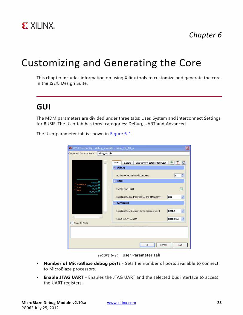
Customizing and Generating the CoreThis chapter includes information on using Xilinx tools to customize and generate the core in the ISE® Design Suite.
GUIThe MDM parameters are divided under three tabs: User, System and Interconnect Settings for BUSIF. The User tab has three categories: Debug, UART and Advanced.
The User parameter tab is shown in Figure 6-1.
• Number of MicroBlaze debug ports - Sets the number of ports available to connect to MicroBlaze processors.
• Enable JTAG UART - Enables the JTAG UART and the selected bus interface to access the UART registers.
X-Ref Target - Figure 6-1
Figure 6-1: User Parameter Tab

MicroBlaze Debug Module v2.10.a www.xilinx.com 24PG062 July 25, 2012
Parameter Values
• Specifies the Bus Interface for the JTAG UART - Selects AXI4-Lite interconnect or PLBv46 bus interface to access the UART registers.
• Specify the JTAG user-defined register used - Select JTAG user-defined register. Can be set to USER1, USER2, USER3 or USER4. Should never need to be changed from USER2, unless there is a conflict with another IP core in the system.
• Select BSCAN location - Selects whether internal or external BSCAN is used. Should never need to be changed from INTERNAL in an embedded system.
The System parameter tab is shown in Figure 6-2.
• Base Address - Base address of the JTAG-based UART. Only used if the UART is enabled.
• High Address - High address of the JTAG-based UART. Only used if the UART is enabled.
Parameter ValuesTo allow the user to obtain an MDM that is uniquely tailored a specific system, certain features can be parameterized in the MDM design. This allows the user to configure a design that only utilizes the resources required by the system. The specif ic features that can be parameterized in Xilinx MDM EDK designs are shown in Table 6-1. See SECTION II: VIVADO DESIGN SUITE, Chapter 4, Customizing and Generating the Core for additional parameters.
X-Ref Target - Figure 6-2
Figure 6-2: System Parameter Tab

MicroBlaze Debug Module v2.10.a www.xilinx.com 25PG062 July 25, 2012
Parameter Values
In addition to the parameters listed in this table, there are also parameters that are inferred for each AXI interface in the EDK tools. Through the design, these EDK-inferred parameters control the behavior of the AXI Interconnect. For a complete list of the interconnect settings related to the AXI interface, see the LogiCORE AXI Interconnect IP Data Sheet [Ref 2].
Allowable Parameter CombinationsThere are no restrictions on parameter combinations for this core.
Table 6-1: EDK MDM Design Parameters
Feature / Description Parameter Name Allowable Values DefaultValue VHDL Type
UART Parameters
Selects the bus interface for the UART C_INTERCONNECT 1 = PLBv46
2 = AXI 1 integer
UART Base Address C_BASEADDR Valid Address(1) None (1) std_logic_vector
UART High Address C_HIGHADDR Valid Address (1) None (1) std_logic_vector
PLB Parameters
PLB address width C_SPLB_AWIDTH 32 32 integer
PLB data width C_SPLB_DWIDTH 32 32 integer
Selects point-to-point or shared PLB topology
C_SPLB_P2P0 = Shared Bus Topology1 = Point-to-Point BusTopology
0 integer
PLB MAster ID Bus Width C_SPLB_MID_WIDTH log2 (C_SPLB_NUM_MASTERS)
with a minimum value of 1 1 integer
Number of PLB Masters C_SPLB_NUM_MASTERS 1-16 1 integer
Width of the Slave Data Bus C_SPLB_NATIVE_WIDTH 32 32 integer
Selects the transactions as being single beat or burst
C_SPLB_SUPPORT_BURSTS0 = Supports only singlebeat transactions 0 integer
AXI4-Lite Parameters
AXI Address Bus Width C_S_AXI_ADDR_WIDTH 32 32 integer
AXI Data Bus Width C_S_AXI_DATA_WIDTH 32 32 integer1. The range specif ied by C_BASESADDR and C_HIGHADDR must be sized and aligned to some power of 2, 2n. Then, the least
n signif icant bits of C_BASEADDR are zero. This range needs to encompass the addresses needed by the MDM UART registers
MicroBlaze Debug Module v2.10.a www.xilinx.com 26PG062 July 25, 2012
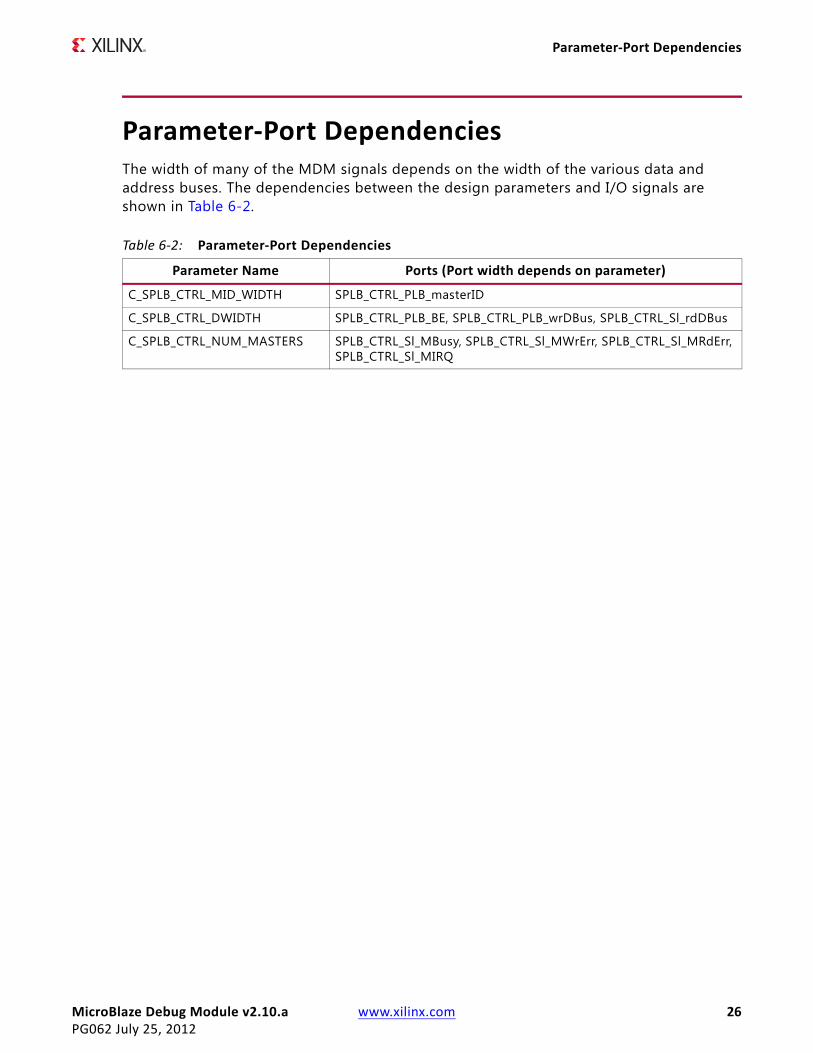
Parameter-Port Dependencies
Parameter-Port DependenciesThe width of many of the MDM signals depends on the width of the various data and address buses. The dependencies between the design parameters and I/O signals are shown in Table 6-2.
Table 6-2: Parameter-Port Dependencies
Parameter Name Ports (Port width depends on parameter)
C_SPLB_CTRL_MID_WIDTH SPLB_CTRL_PLB_masterID
C_SPLB_CTRL_DWIDTH SPLB_CTRL_PLB_BE, SPLB_CTRL_PLB_wrDBus, SPLB_CTRL_Sl_rdDBus
C_SPLB_CTRL_NUM_MASTERS SPLB_CTRL_Sl_MBusy, SPLB_CTRL_Sl_MWrErr, SPLB_CTRL_Sl_MRdErr, SPLB_CTRL_Sl_MIRQ

MicroBlaze Debug Module v2.10.a www.xilinx.com 27PG062 July 25, 2012
Chapter 7
Constraining the CoreSee SECTION II: VIVADO DESIGN SUITE, Chapter 5, Constraining the Core.

MicroBlaze Debug Module v2.10.a www.xilinx.com 28PG062 July 25, 2012
SECTION IV: APPENDICES
Application Software Development
Additional Resources

MicroBlaze Debug Module v2.10.a www.xilinx.com 29PG062 July 25, 2012
Appendix A
Application Software Development
Device DriversThe MDM JTAG-based UART interface is supported by the UART Lite driver, included with Xilinx Software Development Kit.

MicroBlaze Debug Module v2.10.a www.xilinx.com 30PG062 July 25, 2012
Appendix B
Additional Resources
Xilinx ResourcesFor support resources such as Answers, Documentation, Downloads, and Forums, see the Xilinx Support website at:
www.xilinx.com/support.
For a glossary of technical terms used in Xilinx documentation, see:
www.xilinx.com/company/terms.htm.
Solution CentersSee the Xilinx Solution Centers for support on devices, software tools, and intellectual property at all stages of the design cycle. Topics include design assistance, advisories, and troubleshooting tips.
ReferencesThese documents provide supplemental material useful with this user guide:
1. Embedded System Tools Reference Manual (UG111)
2. LogiCORE AXI Interconnect IP Data Sheet (UG768)

MicroBlaze Debug Module v2.10.a www.xilinx.com 31PG062 July 25, 2012
Technical Support
Technical SupportXilinx provides technical support at www.xilinx.com/support for this LogiCORE™ IP product when used as described in the product documentation. Xilinx cannot guarantee timing, functionality, or support of product if implemented in devices that are not defined in the documentation, if customized beyond that allowed in the product documentation, or if changes are made to any section of the design labeled DO NOT MODIFY.
See the Embedded Edition Derivative Device Support web page for a complete list of supported derivative devices for this core.
Revision HistoryThe following table shows the revision history for this document.
Notice of DisclaimerThe information disclosed to you hereunder (the “Materials”) is provided solely for the selection and use of Xilinx products. To the maximum extent permitted by applicable law: (1) Materials are made available “AS IS” and with all faults, Xilinx hereby DISCLAIMS ALL WARRANTIES AND CONDITIONS, EXPRESS, IMPLIED, OR STATUTORY, INCLUDING BUT NOT LIMITED TO WARRANTIES OF MERCHANTABILITY, NON-INFRINGEMENT, OR FITNESS FOR ANY PARTICULAR PURPOSE; and (2) Xilinx shall not be liable (whether in contract or tort, including negligence, or under any other theory of liability) for any loss or damage of any kind or nature related to, arising under, or in connection with, the Materials (including your use of the Materials), including for any direct, indirect, special, incidental, or consequential loss or damage (including loss of data, profits, goodwill, or any type of loss or damage suffered as a result of any action brought by a third party) even if such damage or loss was reasonably foreseeable or Xilinx had been advised of the possibility of the same. Xilinx assumes no obligation to correct any errors contained in the Materials or to notify you of updates to the Materials or to product specifications. You may not reproduce, modify, distribute, or publicly display the Materials without prior written consent. Certain products are subject to the terms and conditions of the Limited Warranties which can be viewed at http://www.xilinx.com/warranty.htm; IP cores may be subject to warranty and support terms contained in a license issued to you by Xilinx. Xilinx products are not designed or intended to be fail-safe or for use in any application requiring fail-safe performance; you assume sole risk and liability for use of Xilinx products in Critical Applications: http://www.xilinx.com/warranty.htm#critapps.© Copyright 2012 Xilinx, Inc. Xilinx, the Xilinx logo, Artix, ISE, Kintex, Spartan, Virtex, Vivado, Zynq, and other designated brands included herein are trademarks of Xilinx in the United States and other countries. All other trademarks are the property of their respective owners.
Date Version Revision
07/25/12 1.0 Initial Xilinx release. This Product Guide is derived from DS641.