micro-processors and assembly programming
TRANSCRIPT

Micro-Processors and AssemblyProgramming
References
• The 8086 Microprocessors Architecture, software and Interfacing techniquesBy: Walter A. Triebel• The 8086/8088 MPU, Architecture, programming and interfacing BY: BarryB. Brey
MicroprocessorA microprocessor or processor (sometimes abbreviated µP) is the heart of thecomputer and it performs all the computational tasks, calculations and dataprocessing etc. inside the computer. Microprocessor is the brain of the computer. ACentral processing unit (CPU) in a computer system or handheld device consistsof one or more microprocessors. The microprocessors can be classified based onthe following features:
1
Instruction Set
It is the set of the instructions that the Microprocessor can execute.
Bandwidth
The number of bits processed by the processor in a single instruction.
4 bit. e.g. Intel 4004
8 bit. e.g. Intel 8085, 8088, Zilog Z80, Z180
16 bit. e.g. Intel 8086, 80186, 80286, 80386,
32 bit. e.g. Intel Pentium, Celeron, AMD Sempron
64 bit. e.g. AMD Athlon.
Clock Speed
Clock speed is measured in the MHz and it determines that how many instructionsa processor can processed.
The speed of the microprocessor is measured in the MHz or GHz. Theprocessor is also known as the CPU (Central Processing Unit). It contains thecontrol unit and the arithmetic unit and both works together to process thecommands. CPU is used in every computer whether it is a workstation, server or alaptop. CPU is a complete computational engine that is designed as a chip. Itstarts the work when you turn on your computer.
CPU is designed to perform the arithmetic and logical operations inside thecomputer. Common operations inside the computer include adding, subtracting,multiplying, comparing the values and fetching the different numbers to processthem. The higher the CPU clocks’ speed the more efficient will be theperformance of the computer.
Computer’s performance is also influenced by the system bus architecture,memory used, type of the processor and software program being running.
Basic Block Diagram of Microprocessor:
Figure 1: Basic Block Diagram of Microprocessor
2

ALU – Performs all arithmetic and logical operations
Register array – Holds the data temporarily for processing
Control Unit – It supervises/ monitors all the operations carried out in thecomputer.
Microcomputer ArchitectureA computer system has three main components: a Central Processing Unit
(CPU) or processor, a Memory Unit and Input Output Units (devices). In anymicrocomputer system, the component which actually processes data is entirelycontained on a single chip called Microprocessor (MPU). This MPU can beprogrammed using assembly language. Writing a program in assembly languagerequires a knowledge of the computer hardware (or Architecture) and the details ofits instruction set.
The main internal hardware features of a computer are the processor, memoryand registers (registers are special processor components for holding address anddata).
The external hardware features are the computer Input/Output devices such askeyboard, monitor…Software consists of the operating system (O.S) and various programs and datafiles stored on disk.
Inside any computer based on a member of the 8086 family, the basic arrangementof the main components is shown in Figure 2.
3

Figure 2: Data flow between the main components of an 8086family computer.
Information is sent from one main component to another along the communicationchannel, which is often called the System Bus. Both programs and data are storedin the memory. The Bus Interface Unit (BIU) within the MPU fetches newinstruction or data as necessary. It is also the BIU jobs to interpret or decodeinstruction and to route results to their proper destination.
The MPU Execution Unit carries out any arithmetic which is required, includingmemory calculation. Microcomputer memories consist of a collection of chips oftwo kinds Read Only Memory (ROM) and Random Access Memories (RAM).
System BusThe components of the computer system must communicate with each other andwith the outside world. Although it may be possible to connect each component tothe CPU separately as a practical matter this would require too many physicalconnects. To keep the number of connections manageable, the processor isconnected to memory and all peripherals using a bus. A Bus is a bunch of wires,and electrical path on the printed IC to which everything in the system isconnected.
4

There are three types of Bus:1- Address Buss (AB): the width of AB determines the amount of physical
memory addressable by the processor.
2- Data Bus (DB): the width of DB indicates the size of the data transferredbetween the processor and memory or I/O device.
3- Control Bus (CB): consists of a set of control signals, typical controlsignals includes memory read, memory write, I/O read, I/O write, interruptacknowledge, bus request. These control signals indicates the type of actiontaking place on the system bus.
Personal Computer (PC) ComponentsThe main component of the PC is its System Board (or mother board). It containsthe processor, co-processor, main memory, connectors, and expansion slots foroptional cards.
The slots and connectors provide access to such components as ROM, RAM, harddisk, CD-ROM drive, additional memory, video unit, keyboard, mouse, paralleland serial device, sound adapter and cache memory (the processor use high speedcache memory to decrease its need to access the slower main memory). A bus withwires attached to the system board connect the components. It transfers databetween the processor, memory and external devices.
A. The processorThe CPU or processor acts as the controller of all actions or services provided bythe system. The operations of a CPU can be reduced to three basic steps: fetch,decode, and execute. Each step includes intermediate steps, some of which are:
1- Fetch the next instruction:- Place it in a holding area called a queue.- Decode the instruction.
2- Decode the instruction- Perform address translation.- Fetch operand from memory.
5

3- Execute the instruction.- Perform the required calculation.- Store results in memory or register.- Set status flag attached to the CPU.
Figure 3 shows a block diagram of a simple imaginary CPU. The CPU is dividedinto two general parts. Arithmetic Logic Unit (ALU) and Control Unit (CU).
- The ALU carry Arithmetic, logical, and shifting operations.- The CU fetches data and instruction, and decodes addresses for the ALU.
Figure 3: A block diagram of a simple CPU.
B. Memory
6

The memory of a computer system consist of tiny electronic switches, with eachswitch set in one of two states: open or close. It is however more convenient tothink of these states as 0 and 1.Thus each switch can represent a binary digit or bit, as it is known, the memoryunit consists of millions of such bits, bits are organized into groups of eight bitscalled byte.
Memory can be viewed as consisting of an ordered sequence of bytes. Each byte inthis memory can be identified by its sequence number starting with 0, as shown inFigure 4. This is referred to as memory address of the byte. Such memory is calledbyte addressable memory.
8086 can address up to 1 MB (220 bytes) of main memory this magic numbercomes from the fact that the address bud of the 8086 has 20 address lines. Thisnumber is referred to as the Memory Address Space (MAS). The memory addressspace of a system is determined by the address bus width of the CPU used in thesystem. The actual memory in a system is always less than or equal to the MAS.
Figure 4: Logical view of the system memory
7

Two basic memory operationsThe memory unit supports two fundamental operations: Read and Write. The readoperation read a previously stored data and the write operation stores a value inmemory. See Figure 5
Figure 5: Block diagram of system memory
Steps in a typical read cycle:1- Place the address of the location to be read on the address bus.2- Activate the memory read control signal on the control bus.3- Wait for the memory to retrieve the data from the address memory location.4- Read the data from the data bus.5- Drop the memory read control signal to terminate the read cycle.
Steps in a typical write cycle:1- Place the address of the location to be written on the address bus.2- Place the data to be written on the data bus.3- Activate the memory write control signal on the control bus.4- Wait for the memory to store the data at the address location.5- Drop the memory write control signal to terminate the write cycle.
Addresses: group of bits which are arranged sequentially in memory, to enabledirect access, a number called address is associated with each group. Addresses
8

start at 0 and increase for successive groups. The term location refers to a group ofbits with a unique address. Table 1 represents Bit, Byte, and Larger units.
Table1: Bit, Byte, and Larger units.
Types of memoryThe memory unit can be implemented using a variety of memory chips- differentspeeds, different manufacturing technology, and different sizes. The two basictypes are RAM and ROM.
1- Read Only Memories (ROM):
ROMs allow only read operation to be performed. This memory is non-volatile.Most ROMs are programmed and cannot be altered. This type of ROM is cheaperto manufacture than other types of ROM. The program that controls the standardI/O functions (called BIOS) is kept in ROM, configuration software.
Other types of ROM include:- Programmable ROM (PROM).- Erasable PROM (EPROM) is read only memory that can be reprogrammed
using special equipment.- EAPROM, Electrically Alterable Programmable ROM is a Read Only
Memory that is electrically reprogrammable.
9
2- Read/Write Memory
Read/Write memory is commonly referred to as Random Access Memory (RAM);it is divided into static and dynamic. Static RAM (SRAM): used for implementingCPU registers and cache memories. Dynamic RAM (DRAM), the bulk of mainmemory in a typical computer system consists of dynamic ram.
Dynamic RAM: main memory, or RAM is where program, data are kept when aprogram is running. It must be refreshed with in less than a millisecond or lossesits contents.
Static RAM, used for special high speed memory called cache memory whichgreatly improves system performance. Static RAM keeps its value without havingto be refreshed.
C. INPUT/OUTPUTInput/output (I/O) devices provide the means by which the computer system caninteract with the outside world. Computers use I/O devices (also called peripheraldevices) for two major purposes:
1- To communicate with the outside world and,2- Store data.
Devices that are used to communicate like, printer, keyboard, modem, Devices thatare used to store data like disk drive. I/O devices are connected to the system busthrough I/O controller (interface) – which acts as interface between the systembus and I/O devices.
There are two main reasons for using I/O controllers
1- I/O devices exhibit different characteristics and if these devices are connecteddirectly, the CPU would have to understand and respond appropriately to each I/Odevice. This would cause the CPU to spend a lot of time interacting with I/Odevices and spend less time executing user programs.
2- The amount of electrical power used to send signals on the system bus is verylow. This means that the cable connecting the I/O device has to be very short (a
10

few centimeters at most). I/O controllers typically contain driver hardware to sendcurrent over long cable that connects I/O devices. See Figure 6.
Figure 6: Block diagram of a generic I/O device interface.
Evolution of Intel MicroprocessorThe principle way in which MPU & microcomputer are categorized in term of themaximum number of binary bit in the data they process that is, their word length.Processor vary in their speed, capacity of memory, register and data bus, below area brief description of various Intel processor in Table 2.
8088 and 8086 functionally identical but 8088 lower performance, 80186 run all8088 and 8086 software, but have 10 new instructions. 80188 in function areidentical to 80186 but lower performances. 80286 run all 8086, 80186 program,but has extra instruction, more powerful than 8086. 80386 has various operationmode, which allow it to act as 80286 chip or multiple 8086 chip, as well as a set ofinstruction capable of 32 bit operations such as arithmetic.
11
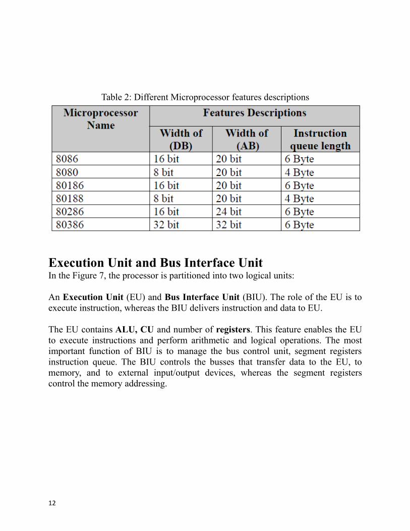
Table 2: Different Microprocessor features descriptions
Execution Unit and Bus Interface UnitIn the Figure 7, the processor is partitioned into two logical units:
An Execution Unit (EU) and Bus Interface Unit (BIU). The role of the EU is toexecute instruction, whereas the BIU delivers instruction and data to EU.
The EU contains ALU, CU and number of registers. This feature enables the EUto execute instructions and perform arithmetic and logical operations. The mostimportant function of BIU is to manage the bus control unit, segment registersinstruction queue. The BIU controls the busses that transfer data to the EU, tomemory, and to external input/output devices, whereas the segment registerscontrol the memory addressing.
12

Figure 7: Execution unit and Bus interface unit.
13

Another function of the BIU is to provide access to instructions, because theinstructions for a program that is executing are kept in memory, the BIU mustaccess instruction from memory and place them in an instruction queue, whichvaries in size depending on the processor. This feature enables the BIU to lookahead and prefetch instructions, so that there is always a queue of instructionsready to execute.
The EU and BIU work in parallel, with the BIU keeping one step ahead. The EUnotifies the BIU when it needs access to data in memory or I/O devices. Also theEU request machine code instructions from the BIU instruction queue. The topinstruction is the currently executable one, and while the EU is occupied executingan instruction, the BIU fetch another instruction from memory. This fetchingoverlaps with execution and speeds up processing.
Addressing Data in MemoryDepending on the model, the processor can access one or more bytes of memory ata time. Consider the Hexa value (0529H) which requires two bytes or one word ofmemory. It consist of high order (most significant) byte 05 and a low order (leastsignificant) byte 29.The processor store the data in memory in reverse byte sequence i.e. the loworder byte in the low memory address and the high order byte in the high memoryaddress. For example, the processor transfer the value 0529H from a register intomemory address 04A26 H and 04A27H like this:
14

The processor expects numeric data in memory to be in reverse byte sequence andprocesses the data accordingly, again reverses the bytes, restoring them to correctlyin the register as hexa 0529H.When programming in assembly language, you have to distinguish between theaddress of a memory location and its contents. In the above example the content ofaddress 04A26H is 29, and the content of address 04A27H is 05.
There are two types of addressing schemes:
1. An Absolute Address, such as 04A26H, is a 20 bit value that directly referencesa specific location.
2. A Segment Offset Address, combines the starting address of a segment with anoffset value.
Segments and AddressingSegments are special area defined in a program for containing the code, the data,and the stack. Segment Offset within a program, all memory locations within asegment are relative to the segment starting address. The distance in bytes from thesegment address to another location within the segment is expressed as an offset(or displacement).
15

To reference any memory location in a segment, the processor combine thesegment address in a segment register with the offset value of that location, that is,its distance in byte from the start of the segment.
Specifying addressesTo represent a segment address and its relative offset we use the notation:
Segment: offset
Thus 020A:1BCD denotes offset 1BCDH from segment 020AH.
The actual address it refers to is obtained in the following way:
1- Add zero to the right hand side of the segment address.2- Add to this the offset.
Hence the actual address referred to by 020A:1BCD is 03C6D.
Address Bus in the 8086 is 20 bits wide (20 lines) i.e. the processor can accessmemory of size 220 or 1048576 bytes (1MB).
16

Instruction Pointer = 16 bit register which means the processor can only address 0– 216 (65535) bytes of memory. But we need to write instructions in any of the1MB of memory. This can be solved by using memory segmentation., where eachsegment register is 16-bit (this 16-bit is the high 16-bit of Address Bus (A4- A19))i.e. each of the segment registers represent the actual address after shifting theaddress 4-bit to get 20 bits.
Registers
Registers are 8, 16, or 32-bit high speed storage locations directly inside the CPU,designed to be accessed at much higher speed than conventional memory.
17

Figure 8: Intel 16-bit registers
The CPU has an internal data bus that is generally twice as wide as its external databus.
Data Registers: The general purpose registers, are used for arithmetic and datamovement. Each register can be addressed as either 16-bit or 8 bit value. Example,AX register is a 16-bit register, its upper 8-bit is called AH, and its lower 8-bit iscalled AL. Bit 0 in AL corresponds to bit 0 in AX and bit 0 in AH corresponds tobit 8 in AX. See Figure 9.
18

Figure 9: AX register
Instructions can address either 16-bit data register as AX, BX, CX, and DX or 8-bitregister as AL, AH, BL, BH, CL, CH, Dl, and DH. If we move 126FH to AX thenAL would immediately 6FH and AH = 12H.
* Each general purpose register has special attributes:
1- AX (Accumulator): AX is the accumulator register because it is favored bythe CPU for arithmetic operations. Other operations are also slightly moreefficient when performed using AX.
2- BX (Base): the BX register can hold the address of a procedure or variable.Three other registers with this ability are SI, DI and BP. The BX register canalso perform arithmetic and data movement.
3- CX (Counter): the CX register acts as a counter for repeating or loopinginstructions. These instructions automatically repeat and decrement CX.
4- DX (Data): the DX register has a special role in multiply and divideoperation. When multiplying for example DX hold the high 16 bit of theproduct.
* Segment Registers: the CPU contain four segment registers, used as baselocation for program instruction, and for the stack.
19

1- CS (Code Segment): The code segment register holds the baselocation of all executable instructions (code) in a program.
2- DS (Data Segment): the data segment register is the default baselocation for variables. The CPU calculates their location using thesegment value in DS.
3- SS (Stack Segment): the stack segment register contain the baselocation of the stack.
4- ES (Extra Segment): The extra segment register is an additional baselocation for memory variables.
* Index registers: index registers contain the offset of data and instructions. Theterm offset refers to the distance of a variable, label, or instruction from its basesegment. The index registers are:
1- BP (Base Pointer): the BP register contain an assumed offset from thestack segment register, as does the stack pointer. The base pointer registeris often used by a 23 subroutine to locate variables that were passed onthe stack by a calling program.
2- SP (Stack Pointer): the stack pointer register contain the offset of the topof the stack. The stack pointer and the stack segment register combine toform the complete address of the top of the stack.
3- SI (Source Index): This register takes its name from the stringmovement instruction, in which the source string is pointed to by thesource index register.
4- DI (Destination Index): the DI register acts as the destination for stringmovement instruction.
Status and Control register:
20

1- IP (Instruction Pointer): The instruction pointer register always contain theoffset of the next instruction to be executed within the current code segment.The instruction pointer and the code segment register combine to form thecomplete address of the next instruction.
2- The Flag Register: is a special register with individual bit positions assigned toshow the status of the CPU or the result of arithmetic operations. The Figure 10describes the 8086/8088 flags register:
Figure 10: Flag Register.
There two basic types of flags: (control flags and status flags)
1- Control Flags: individual bits can be set in the flag register by theprogrammer to control the CPU operation, these are - The Direction Flag(DF): affects block data transfer instructions, such as MOVS, CMPS, andSCAS. The flag values are 0 = up and 1 = down.
- The Interrupt flag (IF): dictates whether or not a system interrupt canoccur. Such as keyboard, disk drive, and the system clock timer. A programwill sometimes briefly disable the interrupt when performing a criticaloperation that cannot be interrupted. The flag values are 1 = enable, 0 =disable.
- The Trap flag (TF): Determine whether or not the CPU is halted after eachinstruction. When this is set, a debugging program can let a programmer toenter single stepping (trace) through a program one instruction at a time.
21

The flag values are 1 = on, 0 = off. The flag can be set by INT 3instruction.
2- Status Flags: The status flags reflect the outcomes of arithmetic and logicaloperations performed by the CPU, these are:
- The Carry Flag (CF): is set when the result of an unsigned arithmeticoperation is too large to fit into the destination for example, if the sum of 71and 99 where stored in the 8-bit register AL, the result cause the carry flag tobe 1. The flag values = 1 = carry, 0 = no carry.
- The Overflow (OF): is set when the result of a signed arithmetic operation istoo wide (too many bits) to fit into destination. 1 = overflow, 0 = nooverflow.
- Sign Flag (SF): is set when the result of arithmetic of logical operationgenerates a negative result, 1= negative, 0 = positive.
- Zero Flag (ZF): is set when the result of an arithmetic of logical operationgenerates a result of zero, the flag is used primarily by jump or loopinstructions to allow branching to a new location in a program based on thecomparison of two values. The flag value = 1 = zero, & 0 = not zero.
- Auxiliary Flag: is set when an operation causes a carry from bit 3 to bit 4 (orborrow from bit 4 to bit 3) of an operand. The flag value = 1 = carry, 0 = nocarry.
- Parity Flag: reflect the number of 1 bit in the result of an operation. If there isan even number of bit, the parity is even. If there is an odd number of bits,parity is odd. This flag is used by the OS to verify memory integrity and bycommunication software to verify the correct transmission of data.
Instruction Execution and Addressing
An assembly language programmer writhe a program in symbolic code and usesthe assembler to translate it into machine code as .EXE program. For programexecution, the system looks only the machine code into memory.
22

Every instruction consists of at least one operation, such as MOV, ADD.Depending on the operation, an instruction may also have one or more operandsthat reference the data the operation is to process.
The basic steps the processor takes in executing an instruction are:
1. Fetch the next instruction to be executed from memory and place it in theinstruction queue.
2. Decode the instruction calculates addressed that reference memory, deliverdata to the Arithmetic Logic Unit, and increment the instruction pointer (IP)register.
3. Execute the instruction, performs the request operation, store the result in aregister or memory, and set flags such as zero or carry where required.
For an .EXE program the CS register provides the address of the beginning of aprogram code segment, and DS provide the address of the beginning of the datasegment.
The CS contains instructions that are to be executed, where as the DS contain datathat the instruction reference. The IP register indicates the offset address of thecurrent instruction in the CS that is to be executed. An instruction operandindicates an offset address in the DS to be referenced.
Consider an example in which the program loader has determined that it is to beload on .EXE program into memory beginning at location 05BE0H. The loaderaccordingly initialize CS with segment address 05BE[0]H and IP with zero.
CS: IP together determine the address of the first instruction to execute 05BE0H +0000H = 05BE0H. In this way the first instruction in CS being execution, if the firstinstruction is two byte long, the processor increment IP by 2, so that , the nextinstruction to be executed is 05BE0H + 0002H = 05BE2H.
Assume the program continues executing, and IP contain the offset 0023H. CS: IPnow determine the address of the next instruction to execute, as follows:
23

EX: let's say that MOV instruction beginning at 0FC03H copies the content of abyte in memory into the AL register. The byte is at offset 0016H in the DS. Here arethe machine code and the symbolic code for this operation.
The second and third byte contains the offset value in reversed byte sequence. Insymbolic code, the operand [0016] in square brackets (an index operator) indicatesan offset value to distinguish it from the actual storage address 16.
Let say that the program has initialized the DS register with DS address 05D1[0]H.To access the data item, the processor determines its location from the segmentaddress in DS + the offset (0016H) in the instruction. Operand become DS contain0FD1[0]H, the actual location of the reference data item is
24
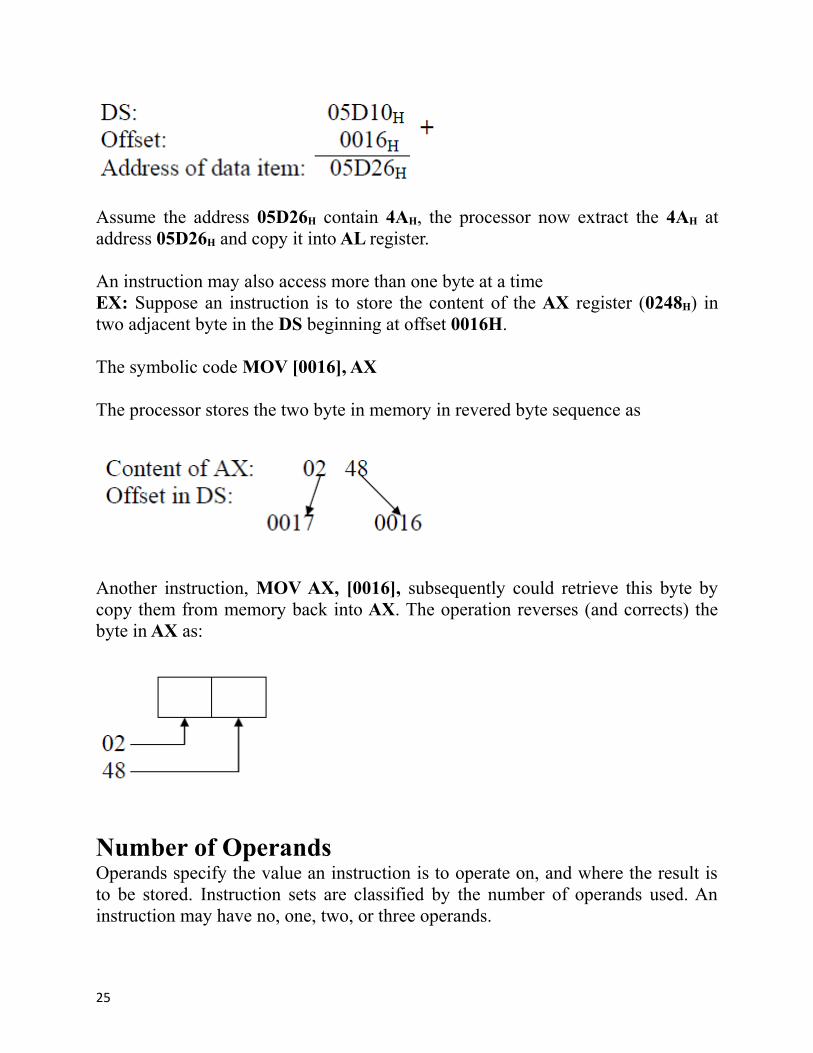
Assume the address 05D26H contain 4AH, the processor now extract the 4AH ataddress 05D26H and copy it into AL register.
An instruction may also access more than one byte at a timeEX: Suppose an instruction is to store the content of the AX register (0248H) intwo adjacent byte in the DS beginning at offset 0016H.
The symbolic code MOV [0016], AX
The processor stores the two byte in memory in revered byte sequence as
Another instruction, MOV AX, [0016], subsequently could retrieve this byte bycopy them from memory back into AX. The operation reverses (and corrects) thebyte in AX as:
Number of OperandsOperands specify the value an instruction is to operate on, and where the result isto be stored. Instruction sets are classified by the number of operands used. Aninstruction may have no, one, two, or three operands.
25

1. Three-Operand instruction:In instruction that have three operands, one of the operand specifies the destinationas an address where the result is to be saved. The other two operands specify thesource either as addresses of memory location or constants.
EX: A=B+CADD destination, source1, source2ADD A,B,C
EX: Y=(X+D)* (N+1)
ADD T1, X, DADD T2, N, 1Mul Y, T1, T2
2. Two operand instructionIn this type both operands specify sources. The first operand also specifies thedestination address after the result is to be saved. The first operand must be anaddress in memory, but the second may be an address or a constant.
ADD destination, sourceEX: A=B+C
MOV A, BADD A, C
EX: Y=(X+D)* (N+1)
MOV T1, XADD T1, DMOV Y, NADD Y, 1MUL Y, T1
3. One Operand instructionSome computer have only one general purpose register, usually called on Acc. It isimplied as one of the source operands and the destination operand in memoryinstruction the other source operand is specified in the instruction as location inmemory.
26

ADD source
LDA source; copy value from memory to ACC.STA destination; copy value from Acc into memory.
EX: A=B+C
LDA BADD CSTA A
EX: Y=(X+D)* (N+1)
LDA XADD DSTA T1LDA NADD 1MUL T1STA Y
4. Zero Operand instructionSome computers have arithmetic instruction in which all operands are implied,these zero operand instruction use a stack, a stack is a list structure in which allinsertion and deletion occur at one end, the element on a stack may be removedonly in the reverse of the order in which they were entered. The process ofinserting an item is called Pushing, removing an item is called Popping.
Computers that use Zero operand instruction for arithmetic operations also use oneoperand PUSH and POP instruction to copy value between memory and the stack.
PUSH source; Push the value of the memory operand onto theTop of the stack.
POP destination; POP value from the Top of the stack and copy itinto the memory operand.
27

Assembly LanguageInstruction
Assembly languageinstructions are provided todescribe each of the basicoperations that can beperformed by amicroprocessor. They arewritten using alphanumericsymbols instead of the 0s and
1s of the microprocessor's machine code. Program written in assembly languageare called source code. An assembly language description of this instruction is
ADD AX, BX
In tins example, the contents of BX and AX are added together and their sum is putin AX. Therefore, BX is considered to be the source operand and AX thedestination operand.
Here is another example of an assembly language statement:
LOOP: MOV AX, BX ; COPY BX INTO AX
This instruction statement starts with the word LOOP. It is an address identifier forthe instruction MOV AX, BX. This type of identifier is called a label or tag. Theinstruction is followed by "COPY BX INTO AX." This part of the statement iscalled a comment. Thus a general format for writing and assembly languagestatement is:
LABEL: INSTRUCTION ; COMMENT
The 8086 Addressing ModeWhen the 8086 executes an instruction, it performs the specified function on data.The data are called its operands and may be part of the instruction reside in one ofthe internal registers of the 8086, stored at an address in memory, or held at an I/Oport. To access these different types of operands, the 8086 is provided with
28

Various addressing modes:
1. Register Addressing Mode
With the register addressing mode, the operand to be accessed is specified asresiding in an internal register of the 8086, an example of an instruction that usesthis addressing mode is
MOV AX, BX
This stands for move the contents of BX, the source operand, to AX, thedestination operand. Both the source and destination operands have been specifiedas the content of the internal registers of the 8086. See Figure 11(a, b).
2. Immediate Addressing Mode
If a source operand is part of the instruction instead of the contents of a register ormemory location, it represents what is called an immediate operand and is accessedusing the immediate addressing mode. Typically, immediate operands representconstant data. Immediate operands can be either a byte or word of data. In theInstruction
MOV AL, 015H
The source operand 15H is an example of a byte-wide immediate source operand.Note that the value of the immediate operand must always be preceded by a zero.See Figure 12(a, b).
29

Figure 11(a): Register addressing mode before execution.
30

Figure 11(b): Register addressing mode after execution.
31

Figure 12(a): Immediate addressing mode before execution.
32
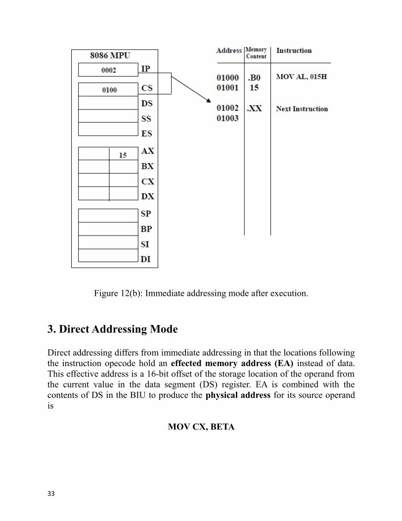
Figure 12(b): Immediate addressing mode after execution.
3. Direct Addressing Mode
Direct addressing differs from immediate addressing in that the locations followingthe instruction opecode hold an effected memory address (EA) instead of data.This effective address is a 16-bit offset of the storage location of the operand fromthe current value in the data segment (DS) register. EA is combined with thecontents of DS in the BIU to produce the physical address for its source operandis
MOV CX, BETA
33

This stands for move the contents of the memory location which is offset by BETAfrom the current value in DS into internal register CX. See Figure 13(a, b). Noticethat the value assigned to constant BETA is 1234H.
PA = 02000H + 1234H
= 03234H
4. Register Indirect Addressing Mode
Register indirect addressing is similar to direct addressing in that an effectiveaddress is combined with the contents of DS to obtain a physical address.However, it differs in the way the offset is specified. This time EA resides in eithera pointer register or index register within the 8086. The pointer register can beeither BX or BP and the index register can be SI or DI.
MOV AX, [SI]
This instruction moves the contents of the memory location offset by the value ofEA in SI from the current value in DS to the AX register. See Figure 14(a, b). SIcontains 1234H and DS contains 0200H.
PA = 02000H + 1234H
= 03234H
34

Figure 13(a): Direct Addressing mode before execution.
35

Figure 13(b): Direct Addressing mode after execution.
Figure 14(a): Register Indirect Addressing before execution.
36
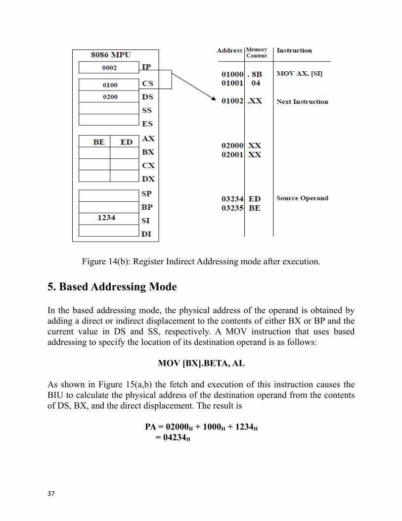
Figure 14(b): Register Indirect Addressing mode after execution.
5. Based Addressing Mode
In the based addressing mode, the physical address of the operand is obtained byadding a direct or indirect displacement to the contents of either BX or BP and thecurrent value in DS and SS, respectively. A MOV instruction that uses basedaddressing to specify the location of its destination operand is as follows:
MOV [BX].BETA, AL
As shown in Figure 15(a,b) the fetch and execution of this instruction causes theBIU to calculate the physical address of the destination operand from the contentsof DS, BX, and the direct displacement. The result is
PA = 02000H + 1000H + 1234H
= 04234H
37

6. Indexed Addressing Mode
Indexed addressing works identically to the based addressing, it uses the contentsof one of the index registers, instead of BX or BP, in the generation of the physicaladdress, here is an example:
MOV AL, ARRAY[SI]
The example in Figure 16(a,b) shows the result of executing the MOV instruction.First the physical address for the source operand is calculated from DS, SI, and thedirect displacement.
PA = 02000H + 2000H + 1234H
= 05234H
Then the byte of data stored at this location, which is BEH is read into lower byteAL of the accumulator register.
38
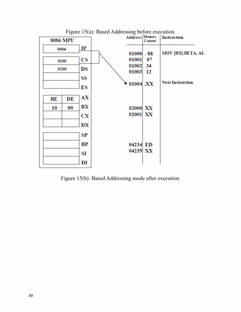
Figure 15(a): Based Addressing before execution.
Figure 15(b): Based Addressing mode after execution.
39
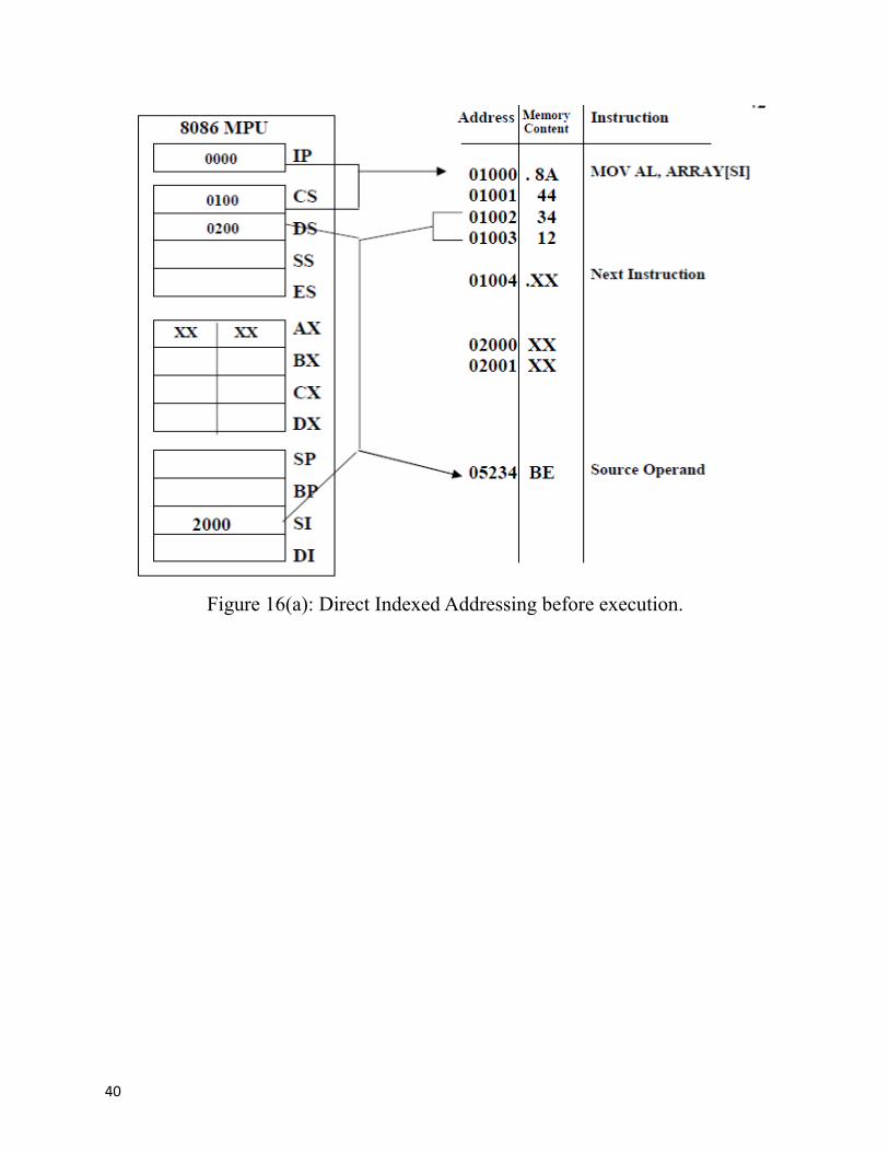
Figure 16(a): Direct Indexed Addressing before execution.
40

Figure 16(b): Direct Indexed Addressing mode after execution.7. Based Indexed Addressing Mode
Combining the based addressing mode and the indexed addressing mode togetherresults in a new, more powerful mode known as based indexed addressing. Let usconsider an example of a MOV instruction using this type of addressing.
MOV AH, [BX].BETA[SI]
An example of executing this instruction is illustrated in Figure 17(a,b). Theaddress of the source operand is calculated as
PA = 02000H + 1000H + 1234H + 2000H
= 06234H
Execution of this instruction causes the Value stored at this location to be writteninto AH.
8. String Addressing Mode
41
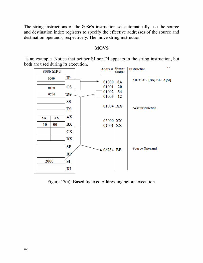
The string instructions of the 8086's instruction set automatically use the sourceand destination index registers to specify the effective addresses of the source anddestination operands, respectively. The move string instruction
MOVS
is an example. Notice that neither SI nor DI appears in the string instruction, butboth are used during its execution.
Figure 17(a): Based Indexed Addressing before execution.
42

Figure 17(b): Based Indexed Addressing mode after execution.9. Port Addressing Mode
Port addressing is used in conjunction with the IN and OUT instructions to accessinput and output ports. Any of the memory addressing modes can be used for theport address for memory mapped ports. For ports in the I/O address space, only theDirect addressing mode and an Indirect addressing mode using DX areavailable. For example, Direct addressing of an input port is used in theinstruction
IN AL, 15H
This stands for input the data from the byte wide input port at address 15H of theI/O address space to register AL. Next, let us consider another example. UsingIndirect port addressing for the source operand in an IN instruction, we get:
IN AL, DX
It means input the data from the byte wide input port whose address is specified bythe contents of register DX. For instance, if DX equals 1234H the contents of theport at this I/O address are loaded into AL.
43

Problems:
1. Which register holds a count for some instruction?2. What is the purpose of the IP register?3. The carry flag bit is set by which arithmetic operation?4. A number that contain 3 one bit said to have---------- parity?5. Find the memory address of the next instruction execute by the micro processorfor the following CS:IP combinations:
a. CS=1000H and IP=2000H
b. CS=2000H and IP=1000H
6. Which register or registers are used as an offset address for string instructiondestination in the microprocessor?7. The stack memory is addressed by a combination of the-------- segment plus ----------- offset.8. Which registers of the 8086 are used in memory segmentation?9. Categorize each flag bit of the 8086 as either a control flag or as a flag tomonitor the effect of instruction execution.10. Identify the three part of an assembly language instruction in each of thefollowing statement:
AGAIN: ADD AX, CX; ADD THE REGISTERSMOV BX, AX; SAVE RESULT
11. Identify the source and destination operand for each of the statements in 10.
Instructions set
8086 has 117 instructions, these instructions divided into 6 groups:
1. Data transfer instructions2. Arithmetic instructions3. Logic instructions4. Shift instructions5. Rotate instructions6. Advance instructions
1. Data Transfer Instructions
44
The microprocessor has a group of data transfer instructions that are provided tomove data either between its internal registers or between an internal register and astorage location in memory. Some of these instructions are:
♣ MOV use to transfer a byte or a word of data from a source operand to adestination operand. These operands can be internal registers and storage locationsin memory. Notice that the MOV instruction cannot transfer data directly betweena source and a destination that both reside in external memory. For instance, flagbits within the microprocessors are not modified by execution of a MOVinstruction.
EXAMPLES:
1. MOV DX, CS where DX=0100H
DX=CS=0100H
2. MOV SUM, AX DS=0200 H SUM=1212H
PA=02000H+1212H = 03212H
AL Memory location 03212H
AH Memory location 03213H
4. If DS contain 1234H what is the effect of executing the instruction MOVCX,[0ABCDH]
CL loaded with the content of Memory location 1234H + ABCDH = 1CF0DH
And CH is loaded with the content of Memory location 1234H + ABCDH +1= 1CF0EH
♣ XCHG: in MOV instruction the original contents of the source location arepreserved and the original contents of the destination are destroyed. But XCHGinstruction can be used to swap data between two general purpose register orbetween a general purpose register and storage location in memory.
EXAMPLES:
1. XCHG AX, DX (AX) (DX)
45

2. XCHG SUM, BX
(DS (0) + SUM) BX DS=02000 H + 1234 H =03234H
(3234) (BL)
(3235) (BH)
2. Arithmetic Instructions
Arithmetic instructions includes instructions for the addition, subtractions can beperformed on numbers expressed in a variety of numeric data formats. The statusthat results from the execution of an arithmetic instruction is recoded in the flags ofthe microprocessor. The flags that are affected by arithmetic instructions are CF,AF, SF, ZF, and PF.
♣ Addition: ADD, ADC, and INC- ADD AX,BX AX= AX+BX
EXAMPLE:
AX= 1100H, BX=0ABCH ADD AX, BX1100H+ 0ABCH = 1BBCH = AX
- ADC AX, BX AX=AX+BX+CF
- INC AH AH= AH +1
EXAMPLE:
The original contents of AX, BL, memory location SUM, and CF are AX=1234H,BL= ABH, Sum=00CDH and CF=0 respectively, describe the result of execution thefollowing sequence of instruction:
46

ADD AX, SUMADC BL, 05H
INC SUM
1. AX= 1234H + 00CDH = 4301H CF=02. BL= ABH +05H +0=B0H CF=03. SUM=00CDH + 1=00CEH CF=0
♣ Subtraction: SUB, SBB, DEC, and NEG- SUB AX, BXAX=AX – BX
- SBB AX, BXAX= AX - BX – CF
EXAMPLE:
BX=1234H, CX=0123H, CF=0SBB BX, CXBX=1234H-0123H-0 =1111H
- DEC subtract 1 from its operand- NEG BX (2's complement)
00H – BX0000 + 2's complement of BX
EXAMPLE:
47

♣ Multiplication and Division MUL, DIV
- MUL CL (AX)= AL* CL
- MUL CX (DX, AX) = AX * CX
- DIV CL (AH), (AL) = AX/CLAnd AL the quotientWhere AH is the reminder
- DIV CX DX, AX= (DX,AX)/CX AX contain the Quotient DX contain the reminder
EXAMPLE:
MUL CL where AL=-1 CL= -2AX= FF H * FE H = FD02 H
3. Logical Instructions (AND, OR, XOR, NOT)
48

4. Shift InstructionsThe four types of shift instructions can perform two basic types of shift operations.They are the logical shift and arithmetic shift. Each of these operations can beperformed to the right or to the left.
49

5. Rotate Instructions
♣ ROL (Rotate Left)
♣ ROR (Rotate Right)
♣ RCL (Rotate Carry Left)
50

♣ RCR (Rotate Carry Right)
5. Advance instruction (Program and Control Instruction)In this section many of instructions that can be executed by the 8086microprocessor are described, furthermore, these instructions use to write simpleprograms. The following topics are discussed in this section:
1. Flag control instructions2. Compare instruction3. Jump instructions4. String instruction
1. Flag Control InstructionThe 8086 microprocessor has a set of flags which either monitor the status ofexecuting instruction or control options available in its operation. The instructionset includes a group of instructions which when execute directly affect the settingof the flags. The instructions are:
LAHF: load AH from flagsSAHF: store AH into flagsCLC: clear carry, CF=0STC: set carry, CF=1
CMC: complement carry, CF= CFCLI: clear interrupt, IF=0STI: set interrupt, IF=1
EXAMPLE:
51
Write an instruction to save the current content of the flags in memory locationMEM1 and then reload the flags with the contents of memory location MEM2
Solution:LAHFMOV MEM1, AHMOV AH, MEM2SAHF
2. Compare InstructionThere is an instruction included instruction set which can be used to compare two8-bit number or 16-bit numbers. It is the compare (CMP) instruction.
The operands can reside in a storage location in memory, a register within theMPU. Instruction Meaning Format Operation Flag affected the process ofcomparison performed by the CMP instruction is basically a subtraction operation.The source operand is subtracted from the destination operand. However the resultof this subtraction is not saved. Instead, based on the result the appropriate flagsare set or reset.
EXAMPLE:
Lets the destination operand equals 100110012and that the source operand equals000110112. Subtraction the source from the destination, we get
10011001 00011011
52

Replacing the destination operand with its 2's complement and adding
10011001 11100101
011111102
1. No carry is generated from bit 3 to bit 4, therefore, the auxiliary carry flag AF isat logic 0.
2. There is a carry out from bit 7. Thus carry flag CF is set.3. Even through a carry out of bit 7 is generated; there is no carry from bit 6 to bit
7. This is an overflow condition and the OF flag is set.4. There are an even number of 1s, therefore, this makes parity flag PF equal to 1.5. Bit 7 is zero and therefore sign flag SF is at logic 0.6. The result that is produced is nonzero, which makes zero flag ZF logic 0.
3. JUMP Instruction
The purpose of a jump instruction is to alter the execution path of instructions inthe program. The code segment register and instruction pointer keep track of thenext instruction to be executed. Thus a jump instruction involves altering thecontents of these registers. In this way, execution continues at an address other thanthat of the next sequential instruction. That is, a jump occurs to another part of theprogram.There two type of jump instructions:
a. Unconditional jump.b. Conditional jump.
In an unconditional jump, no status requirements are imposed for the jump tooccur. That is, as the instruction is executed, the jump always takes place to changethe execution sequence. See Figure 17 Instruction Meaning Format OperationFlags affected
53
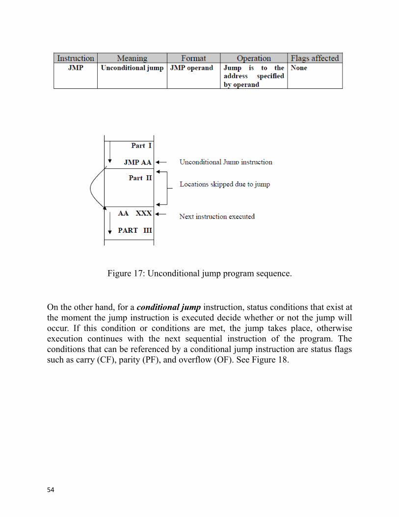
Figure 17: Unconditional jump program sequence.
On the other hand, for a conditional jump instruction, status conditions that exist atthe moment the jump instruction is executed decide whether or not the jump willoccur. If this condition or conditions are met, the jump takes place, otherwiseexecution continues with the next sequential instruction of the program. Theconditions that can be referenced by a conditional jump instruction are status flagssuch as carry (CF), parity (PF), and overflow (OF). See Figure 18.
54

The following table lists some of the conditional jump instructions:
55
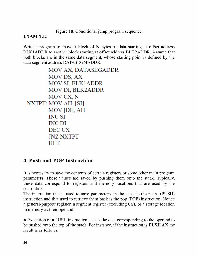
Figure 18: Conditional jump program sequence.EXAMPLE:
Write a program to move a block of N bytes of data starting at offset addressBLK1ADDR to another block starting at offset address BLK2ADDR. Assume thatboth blocks are in the same data segment, whose starting point is defined by thedata segment address DATASEGMADDR.
4. Push and POP Instruction
It is necessary to save the contents of certain registers or some other main programparameters. These values are saved by pushing them onto the stack. Typically,these data correspond to registers and memory locations that are used by thesubroutine. The instruction that is used to save parameters on the stack is the push (PUSH)instruction and that used to retrieve them back is the pop (POP) instruction. Noticea general-purpose register, a segment register (excluding CS), or a storage locationin memory as their operand.
♣ Execution of a PUSH instruction causes the data corresponding to the operand tobe pushed onto the top of the stack. For instance, if the instruction is PUSH AX theresult is as follows:
56

((SP)-1) (AH)
((SP)-2) (AL)
(SP) (SP)-2
This shows that the two bytes of the AX are saved in the stack part of memory andthe stack pointer is decrement by 2 such that it points to the new top of the stack.
♣ On the other hand, if the instruction is
POP AX
Its execution results in
(AL) ((SP))
(AH) ((SP) + 1)
(SP) (SP)+2
The saved contents of AX are restored back into the register.
♣ We also can save the contents of the flag register and if saved we will later haveto restore them. These operations can be accomplished with the push flags(PUSHF) and pop flags (POPF) instructions, respectively. Notice the PUSHFsave the contents of the flag register on the top of the stack. On the other hand,POPF returns the flags from the top of the stack to the flag register.
5. String Instructions
57

The microprocessor is equipped with special instructions to handle stringoperations. By "string" we mean a series of data words or bytes that reside inconsecutive memory locations.There are five basic string instructions in the instruction set of the 8086, theseinstruction are:a. Move byte or work string (MOVS, MOVSB, and MOVSW).b. Compare string (CMPS).c. Scan string (SCAS).d. Load string (LODS)e. Store string (STOS).
They are called the basic string instructions because each defines and operationsfor one element of a string.
Move String
The instructions MOVES, MOVSB, and MOVSW all perform the same basicoperation. An element of the string specified by the source index (SI) register withrespect to the current data segment (DS) register is moved to the location specifiedby the destination index (DI) register with respect to the current extra segment (ES)register.
After the move is complete, the contents of both SI and DI are automaticallyincremented or decremented by 1 for a byte move and by 2 for a word move.Remember the fact that the address pointers in SI and DI increment or decrementdepends on how the direction flag DF is set.
Compare Strings and Scan Strings
The CMPS instruction can be used to compare two elements in the same ordifferent strings. It subtracts the destination operand from the source operand andadjusts flags CF, PF, AF, ZF, SF, and OF accordingly. The result of subtraction isnot saved; therefore, the operation does not affect the operands in any way
CMPS BYTE
The source element is pointed to by the address in SI with respect to the currentvalue in DS and the destination element is specified by the contents of DI relative
58

to the contents of ES. Both SI and DI are updated such that they point to the nextelements in their respective string.
The scan string (SCAS) instruction is similar to CMPS, however, it compares thebyte or word element of the destination string at the physical address derived fromDI and ES to the contents of AL or AX, respectively. The flags are adjusted basedon this result and DI incremented or decremented.
Interrupts (INTs)
Interrupt is a mechanism by which a program's flow of control can be altered, INTprovide a mechanism to transfer control to an interrupt service routine (ISR).
This mechanism is similar to that of a procedure call however, while procedurecan be invoked only by a procedure call in software. INT can be invoked by bothhardware and software. For instance, when an interrupt signal occurs indicatingthat an external device, such as a printer, requires service. The microprocessormust suspend what it is doing in the main part of the program and pass control to aspecial routine that performs the function required by the device.
The section of program to which control is passed is called the interrupt serviceroutine (ISR). When the microprocessor terminates execution in the main program,it remembers the location where it left off and then picks up execution with thefirst instruction in the service routine. After this routine has rum to completion,program control is returned to the point where the microprocessor originally leftthe main body of the program.
The interrupts of the microprocessors include two hardware pins that requestinterrupts (INTR and NMI), and one hardware pin (INTA) that acknowledges theinterrupt requested through INTR. In addition to the pins, the microprocessor alsohas software interrupts INT, INTO, INT3 and BOUND. Two flag bits IF and TFare also used with the interrupt structure and a special return instruction IRET.
All Interrupt whether HW-initiated or SW-initiated, are identify by an INT-Typenumber that is between (0 and 255), this INT number is used to access the interruptvector table (IVT) to get the associated interrupt vector. HW interrupt can bemasked or disable by manipulating the INT flag using (STI and CLI) instruction.
Interrupt Processing
59

The Interrupt Vector Table (IVT) is located at address 0, each vector takes 4 bytes.Each vector consist of a (CS:IP) pointer to the associated ISR, 2 byte for specifyingthe CS, and 2 byte for the offset (IP) within the CS. As shown in the below Figure(19).
The IVT layout in the memory since each entry in the IVT is 4 byte long, INT typeis multiplied by 4 to get the corresponding ISR pointer in the table. For example ,INT 2 can find the ISR pointer at memory address 2*4 =00008H, the first 2 byte atthe specified address are taken as the offset value, and the next 2 byte as the CSvalue. Thus executing INT 2 causes the CPU to suspend its current program andcalculate the address in the IVT (which is 2*4=8) and read CS:IP value andtransfer control to that memory location.
Just like procedure ISR, should end with a (RET) inst to send control back to theINT program. The interrupt return (IRET) is used for this purpose. On receiving anINT, flag register is automatically saved on the stack. The INT enable flag is clear.This disable attending further INT until this flag is set. Usually, this flag is set inISR unless there is a special reason to disable other INT.
60

Figure 19
61

The current CS and IP values are pushed onto the stack. In most cases, these valueCS and IP point to the instruction following the current instruction the CS and IPregister are loaded with the address of ISR from the IVI.
When an interrupt occur, the following action are taken:
1. Push flag register on the stack2. Clear IF and TF3. Push CS and IP register, on the stack4. Load CS with the 16-bit data at memory address (INT-type *4+2)5. Load IP with the 16 bit data at memory address (INT-type *4).
The last instruction of ISR is (IRET) instruction, it actions are:
1. POP the 16-value on top of stack into IP register2. POP the 16-value on top of stack into CS register3. POP the 16-value on top of stack into flag register.
Interrupt Type
The 8086 microcomputer is capable of implementing any combination of up to 256interrupts. They are divided into five groups: external hardware interrupts, softwareinterrupts, internal interrupts, the nonmaskable interrupt, and the reset interrupt.The function of the external hardware, software, and nonmaskable interrupt and therest interrupts can be defined by the user. On the other hand, the internal and resetinterrupts have dedicated system functions.
Software Interrupt (SW INT)
Are initiated by execution an INT instruction the format is
INT INT-Type Where INT-Type is an integer number in the range 0-255, thus a total of 256different types are possible.
62

Hardware Interrupt (HW INT)
This type is usually use by peripheral I/O devices such as KB to alter CPU thatthey require its attention.
HW INT can be divided into Maskable and Non-Maskable (NMI).
A NMI can be generated by applying an electronic signal on the NMI pin this INTis called NMI because the CPU always respond to this signal. In other word, thisINT cannot be disabling under program control, the NMI cussed by INT2.
Most HW INT are maskable type, and electronic signal should be applied to theINTR (interrupt request) input pin of 8086, 8086 recognize the INTR only if IF=1,thus this INT can be masked or disable by clear IF(IF=0).
NMI vs. Maskable INT
NMI is always attended to by the CPU immediately. Note that when we sayimmediately, the CPU does not suspend the execution of the current inst in themiddle, it complete the current inst and then service the INT.
Maskable INT can be delayed until execution reaches a convenient point. As anexample, let us assume that the CPU is execution main program , an INT occur, asa result, the CPU suspend the main as soon as it finish the current inst of main andthen control is transfer to the ISR. If ISR has to be executed without any interrupt,the CPU can mask further INT until ISR is complete. Suppose that, whileexecuting ISR another mskable INT occurs, service to this INT would have to waituntil ISR is completed.
There are several INT predefined by Microprocessor which have dedicatedfunction this is some of them:
INT 0 Divide error INT the CPU generate an IT type whenever executing a DIVresult in a quotient that is larger than the destination. The default ISR displays adivide overflow message and terminate a program.
Single Step INT, single step is a useful debugging tool to observe of the behaviorof a program instruction by instruction. To start single stepping the TF bit in flag
63

register should be set (TF=1), when TF=1, the CPU automatically generate a type 1INT after execution each inst.
To end single step, TF should be cleared, the CPU however does not have anyinstruction to manipulate the TF directly
♣ Set trap flag (TF=1) to start single stepping
PUSHFPOP AX ;COPY FLAGS INTO AXOR AX, 100H ;SET TF=1PUSH AX ;COPY MODIFY FLAG BIT BACK TO FLAG REGISTERPOPF
♣ Clear trap flag (TF=0) to end single stepping
PUSHFPOP AX ; COPY FLAGS INTO AXAND AX, 0FEFFH, ;CLEAR TF=0PUSH AX ; COPY MODIFY FLAG BIT BAXK TO FLAG REGISTERPOPF
How can more than one device interrupt?
Computer typically have more than one I/O device requesting interrupt service,like keyboard, hard disk, floppy disk, printer all generate an INT when theyrequired the attention to CPU.
When more than one device INT CPU, we need a mechanism to priority these INT(if they come at the same time) and forward only one INT request at a time to theCPU while keeping other INT request pending for their service.
Input and Output
Input & Output (I/O) devices provide the means by which a computer system caninteract with the outside worlds.
64

An I/O device can be a purely input device (e.g. KB, Mouse), a purely outputdevice (printer, screen), or both input and output device like (e.g. disk).
Regardless of the intended purpose of I/O devices, all communication with thesedevices must involve the system bus. However, I/O devices are not directlyconnected to the system bus. Instead, there is usually, On I/O controller that acts asan interface between the system and the I/O devices.
Accessing I/O devices
As programmer, you can have direct control to any of the I/O devices (throughtheir associated I/O controller).
It is a waste of time and effort if everyone had to develop their own routines toaccess I/O devices. In addition system resource could be abused eitherintentionally or accidentally. For instance, and improper disk drive could erase thecontent of a disk due to a bug in the driver routine.
To avoid this problem and to provide a standard way of accessing I/O devices, OSprovide routine to convent all access I/O devices. Typically, access to I/O devicescan be obtain from two layer of system software, the basic I/O system (BIOS) andthe OS,BIOS is ROM resident and is a collection of routine that control the I/Odevices. Both provide access to routine that control I/O devices through amechanism called INT (interrupt).
I/O Address Space and Data Transfer
As we know I/O ports in the 8086 MPU can be either byte wide or word wide. Theport that is accessed for input or output of data is selected by an I/O address. Theaddress is specified as port of the instruction that performs the I/O operation.
I/O addresses are 16 bit in length and are output by the 8086 to the I/O interfaceover bus lines AD0 through AD15, the most significant bit A16-A19 of thememory address are held at the 0 logic (not used).
Below Figure 20 show a map of I/O address space of the 8086 system. This is anindependent 64-KB address space that is dedicated for I/O devices. Notice that itsaddress range is from 000016-FFFF16. Moreover, notice that the eight ports
65

located from address 00F8 to 00FF are specified as reserved. These port addressesare reserved by Intel for use in their future HW and SW products.
Figure 20: I/O Address Space
Data transfer between the MPU and I/O devices are performed over the data bus.Word transfer take place over the complete data bus D0 to D15, and can requiredeither one or two bus cycle.
Ports: a port is a device that connects the processor to the external world through aport processor, receive a signal from an input device and send a signal to an outputdevice.
Input / Output InstructionThe instruction set contains one type of instruction that transfer information to anI/O device (OUT) and another to read information from an I/O device (IN).
• ACC = AL or AX
66

Example 1: write a sequence of inst that will output FF16 to a byte wide outputport at address AB16 of the I/O addresses space.Solution: first the AL register is loaded with FF16 as an immediate operand in theinstruction
MOV AL, 0FFH
Now the data in AL can be output to the byte wide output port with the instruction
OUT 0ABH, AL
Example2: write a series of instruction that will output FF16 to an output portlocated at address B00016 of the I/O address space.
Solution : the DX register must first be loaded with the address of the output port
MOV DX, 0B000H
Next, the data that is to be output must be loaded into AL
MOV AL, 0FFH
Finally, the data are output with the instruction
OUT DX, AL
Example 3: data are to be read in from two byte wide input port at address AA16and A916 respectively, and then output to a word wide output port at addressB00016. Write a sequence of instruction to perform this I/O operation:
Solution: we first read in a byte from the port at address AA16 into AL and moveit to AH
IN AL, 0AA16
MOV AH, AL
The other byte can be read into AL
IN AL, 0A9H
67
To writhe out the word of data in AX, we can load DX with the addressB00016 anduse a variable output instruction
MOV DX, 0B000H
OUT DX, AX
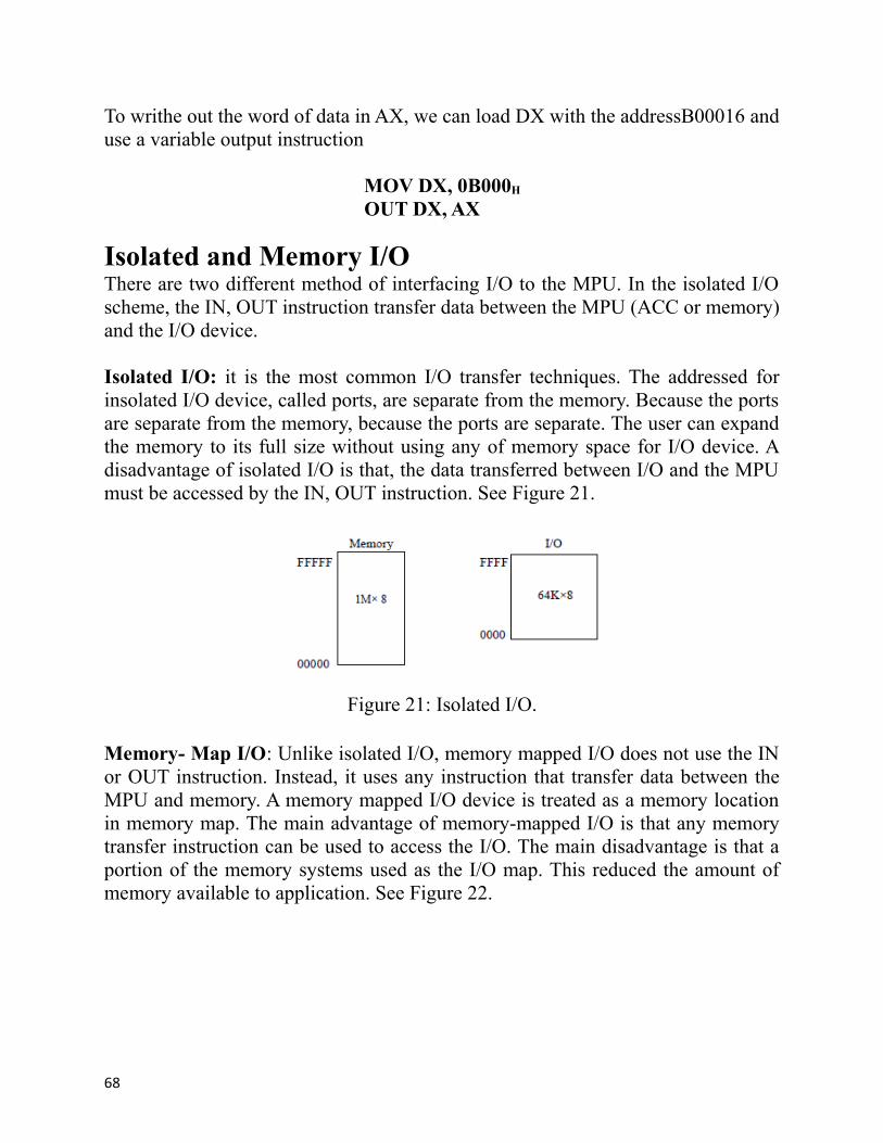
Isolated and Memory I/OThere are two different method of interfacing I/O to the MPU. In the isolated I/Oscheme, the IN, OUT instruction transfer data between the MPU (ACC or memory)and the I/O device.
Isolated I/O: it is the most common I/O transfer techniques. The addressed forinsolated I/O device, called ports, are separate from the memory. Because the portsare separate from the memory, because the ports are separate. The user can expandthe memory to its full size without using any of memory space for I/O device. Adisadvantage of isolated I/O is that, the data transferred between I/O and the MPUmust be accessed by the IN, OUT instruction. See Figure 21.
Figure 21: Isolated I/O.
Memory- Map I/O: Unlike isolated I/O, memory mapped I/O does not use the INor OUT instruction. Instead, it uses any instruction that transfer data between theMPU and memory. A memory mapped I/O device is treated as a memory locationin memory map. The main advantage of memory-mapped I/O is that any memorytransfer instruction can be used to access the I/O. The main disadvantage is that aportion of the memory systems used as the I/O map. This reduced the amount ofmemory available to application. See Figure 22.
68

Figure 22: Memory-Mapped I/O
69