micro and nano-indentation of mosi2
TRANSCRIPT
J O U R N A L O F M A T E R I A L S S C I E N C E 3 9 (2 0 0 4 ) 3769 – 3772 L E T T E R S
Micro and nano-indentation of MoSi2
M. HENZEL, J. KOVALC IK, J. DUSZA∗Department of Structural Ceramics, Institute of Materials Research of the Slovak Academy of Sciences,Watsonova 47, 04353 Kosice, SlovakiaE-mail: [email protected]
A. JUHASZ, J. LENDVAIDepartment of General Physics, ELTE, Pazmany Peter setany 1/A, 1117 Budapest, Hungary
Molybdenum disilicide based materials are candidatefor high temperature structural applications, such as afurnace heating element and an electrical conductor insilicon intergrated circuit design or parts of engines [1].MoSi2 exhibits a high melting point (2030 ◦C), excel-lent high temperature oxidation resistance, and poss-eses many convenient properties such as high stiffness,high thermal conductivity, relatively low density, andhigh strength at elevated temperatures. However, a ma-jor difficulty in application of these materials is thelack of adequate ductility and fracture toughness be-low 1000 ◦C. Only toward the higher temperatures (be-tween 1000 and 1400 ◦C), with the onset of dislocationclimb and diffusional creep processes, does MoSi2 ex-hibit significant plasticity in compression, bending, andtension in both single crystals and polycrystalline ma-terials [2, 3]. During the last decade many approacheshad been applied to reduce the brittle-to-ductile tran-sition temperature (BDTT) of these materials, to over-come the limitation of dislocation mobility and dislo-cation density, and to enhance the capability for plas-tic flow and increase the fracture toughness. The mainapproaches for ductility enhancement are solid solu-tion alloying, second phase microstructure control, duc-tile phase toughening, and high temperature prestrain[4].
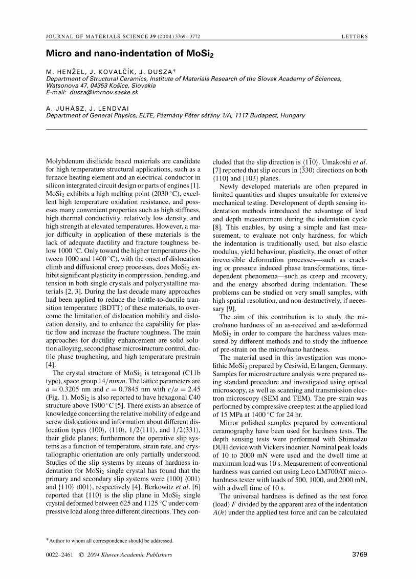
The crystal structure of MoSi2 is tetragonal (C11btype), space group 14/mmm. The lattice parameters area = 0.3205 nm and c = 0.7845 nm with c/a = 2.45(Fig. 1). MoSi2 is also reported to have hexagonal C40structure above 1900 ◦C [5]. There exists an absence ofknowledge concerning the relative mobility of edge andscrew dislocations and information about different dis-location types 〈100〉, 〈110〉, 1/2〈111〉, and 1/2〈331〉,their glide planes; furthermore the operative slip sys-tems as a function of temperature, strain rate, and crys-tallographic orientation are only partially understood.Studies of the slip systems by means of hardness in-dentation for MoSi2 single crystal has found that theprimary and secondary slip systems were {100} 〈001〉and {110} 〈001〉, respectively [4]. Berkowitz et al. [6]reported that {110} is the slip plane in MoSi2 singlecrystal deformed between 625 and 1125 ◦C under com-pressive load along three different directions. They con-
∗Author to whom all correspondence should be addressed.
cluded that the slip direction is 〈 ¯110〉. Umakoshi et al.[7] reported that slip occurs in 〈330〉 directions on both{110} and {103} planes.
Newly developed materials are often prepared inlimited quantities and shapes unsuitable for extensivemechanical testing. Development of depth sensing in-dentation methods introduced the advantage of loadand depth measurement during the indentation cycle[8]. This enables, by using a simple and fast mea-surement, to evaluate not only hardness, for whichthe indentation is traditionally used, but also elasticmodulus, yield behaviour, plasticity, the onset of otherirreversible deformation processes—such as crack-ing or pressure induced phase transformations, time-dependent phenomena—such as creep and recovery,and the energy absorbed during indentation. Theseproblems can be studied on very small samples, withhigh spatial resolution, and non-destructively, if neces-sary [9].
The aim of this contribution is to study the mi-cro/nano hardness of an as-received and as-deformedMoSi2 in order to compare the hardness values mea-sured by different methods and to study the influenceof pre-strain on the micro/nano hardness.
The material used in this investigation was mono-lithic MoSi2 prepared by Cesiwid, Erlangen, Germany.Samples for microstructure analysis were prepared us-ing standard procedure and investigated using opticalmicroscopy, as well as scanning and transmission elec-tron microscopy (SEM and TEM). The pre-strain wasperformed by compressive creep test at the applied loadof 15 MPa at 1400 ◦C for 24 hr.
Mirror polished samples prepared by conventionalceramography have been used for hardness tests. Thedepth sensing tests were performed with ShimadzuDUH device with Vickers indenter. Nominal peak loadsof 10 to 2000 mN were used and the dwell time atmaximum load was 10 s. Measurement of conventionalhardness was carried out using Leco LM700AT micro-hardness tester with loads of 500, 1000, and 2000 mN,with a dwell time of 10 s.
The universal hardness is defined as the test force(load) F divided by the apparent area of the indentationA(h) under the applied test force and can be calculated
0022–2461 C© 2004 Kluwer Academic Publishers 3769

Figure 1 Tetragonal unit cell of MoSi2.
from the following equation [10]:
HU = F/26.43 h2 (1)
where F is the applied load in N and h is the indentationdepth in mm.
The plastic hardness is the quotient from the test forcedivided by an area calculated by the extrapolation:
HUplast = Fmax/26.43 h2r (2)
where Fmax is the maximum force (load) in N and hris the indentation depth resulting as the intersection ofthe tangent of indentation depth curve at the maximumforce (range of the removal of test force) with the in-dentation depth axis in mm.
With the known Young’s modulus of the tested ma-terial, an analytic solution separates the contributionof elastic deformation, converting HU into the conven-tional hardness HV, which is related to the plastic indentsize. HV is calculated from the following equation:
HUplast = 4HU/{1 + √(1 − 12HU/E∗)}2 (3)
where E∗ is the effective contact stiffness, which canbe determined from the equation [11]
E∗ = {(1 − ν2
s
)/Es + (
1 − ν2i
)/Ei
}−1(4)
where Ei is Young’s modulus of the indenter, νi is Pois-son’s ratio of the indenter, Es is Young’s modulus of thetested material, and νs is Poisson’s ratio of the testedmaterial.
The conventional Vickers hardness is calculated fromthe equation
HV = 1.8544F/a2 (5)
where F is the applied force (load) in kg and a is thediagonal of the indentation in mm.
The microstructure of the studied material is shown inFig. 2. Using SEM and EDX it was found that there werethree different phases present in the microstructure of
Figure 2 Microstructure of MoSi2.
the monolithic MoSi2:MoSi2 matrix grains, SiO2, anda little Mo5Si3 (hexagonal Nowotny phase).
Figs 3 and 4 present different F–h curves obtainedfor the MoSi2 intermetallics under study. Values of theuniversal hardness and plastic hardness are recordedin the same figure. The approximate value of hardnesscan be taken from the steady-state curve of universaland plastic hardness. Values of the universal and plas-tic hardness taken from the steady-state curves are pre-sented in Table I. Values of the conventional Vickershardness are presented in Table II.
Both universal and conventional hardness exhibit ob-vious load size effect; the hardness increases with de-creasing indentation depth. Similar load size effect hasbeen found in many ceramics, but also in MoSi2 [12–14]. Boldt et al. [13] investigated microhardness of aMoSi2 single crystal using Vickers indentation withloads from 50 to 14 000 mN. A constant hardness ofapproximately 10 GPa was found until the applied loadhas been reduced to approximately 2000 mN. At thispoint the hardness values begin to increase toward avalue of 19 GPa at the 50 mN load. Morris et al. [14]studied the conventional Vickers microhardness of amonolithic, reactive sintered polycrystalline MoSi2 atloads from 500 to 1000 mN. Microhardness values ofthe materials changed from 12.4 to 14.3 GPa in de-pendence on the sintering temperature. These results
TABLE I Hardness values calculated from the −P–h curves
Microhardness (GPa)
As-received state As-deformed stateMax. load(mN) HU HUplast HU HUplast
500 7.66 9.19 5.51 6.2550 10.78 14.17 9.35 11.77
TABLE I I Traditional Vickers microhardness values
Microhardness (GPa)
As-received state As-deformed stateMax. load(mN) HV HV
500 13.34 11.781000 11.27 10.042000 10.84 10.44
3770

Figure 3 Depth-sensing curve of the as-received state with the maximum load of 50 mN.
Figure 4 Depth-sensing curve of the as-deformed state with the maximum load of 500 mN.
are in full agreement with our results achieved on theas-received material.
Ullmer et al. [15] compared the instrumented andconventional hardness tests for testing different ad-vanced ceramics. There does not exist a systematic re-lationship between the conventional Vickers and plastichardness of the tested materials. The plastic hardnesscorresponds with the conventional Vickers hardnessfor specimens qualified for reference materials only,and both hardness values become significantly differ-ent for commercial engineering materials with higherporosity.
In Figs 5 and 6 shapes of the P–h curves are illus-trated for the as-received and as-deformed materials atthe maximum load of 500 and 50 mN, respectively. Dif-ferences in the shape of P–h curves in the as-receivedand as-deformed materials demonstrates that the as-deformed material has a higher deformation ability and
is softer when compared with the as-received one. Suchbehaviour is more evident when tested at the maximumload of 500 mN. Similar behaviour has been recognizedalso during the conventional Vickers hardness test, butthe difference between the hardness of the as-receivedand as-deformed materials is significantly lower. It canbe explained by the presence of slip systems in the as-deformed material being activated during the pre-strainprocedure. To verify this assumption additional exper-iments have to be performed.
A distinct indentation load size effect was found forthe universal, plastic, and conventional Vickers hard-ness of the as-received and as-deformed MoSi2. Theplastic hardness was lower in comparison to the con-ventional Vickers hardness for both materials and at allindentation loads. The pre-strain can change deforma-tion ability and hardness of the MoSi2 even at roomtemperature.
3771

Figure 5 Comparisons of the P–h curves for the as-received and as-deformated states with the maximum load of 500 mN.
Figure 6 Comparisons of the P–h curves for the as-received and as-deformated states with the maximum load of 50 mN.
AcknowledgmentsThis work was realized with the financial support of theSlovak Grant Agency, under the contract No. 2/1166/21and by NANOSMART, Centre of Excellence, SAS.
References1. A . K . V A S U D E V A N and J . J . P E T R O V I C , Mater. Sci. Eng.
A 155 (1992) 1.2. O . U N A L, J . J . P E T R O V I C , D. H. C A R T E R and T . E .
M I T C H E L L , J. Amer. Ceram. Soc. 73 (6) (1990) 1752.3. T . E . M I T C H E L L, R . G . C A S T R O and J . J . P E T R O V I C ,
Mater. Sci. Eng. A 155 (1992) 241.4. R . G I B A L A, H. C H A N G, C. M. C Z A R N I K and J . P .
C A M P B E L L , Mater. Sci. Eng. A 261 (1999) 122.5. S . I N O U, N. T O Y O K U R A, T . N A K A M U R A, M. M A E D A
and M. T A K A G I , J. Electro. Soc. 130(7) (1983) 1603.6. J . B E R K O W I T Z-M A T T U C K and M. R O S S E T T I N A S W -
1887, Cambridge, MA, 1971.
7. Y . U M A K O S H I and T . S A K A G A M I et al., 59(4) (1989)159.
8. W. C . O L I V E R and G. M. P H A R R J. Mater. Res. 7 (1992)1564.
9. A . J . B U S H B Y , Nondestructive Testing and Evaluation 17 (2001)213.
10. D I N 20339 Universalharteprufung, October 1997.11. A . K R E L L and S . S C H A D L I C H , Mater. Sci. Eng. A 307 (2001)
172.12. J . D U S Z A .13. P . H . B O L D T, J . D . E M B U R R Y and G. C . W E A T H E R L Y ,
Mater. Sci. Eng. A 155 (1992) 251.14. D . G . M O R R I S , M. L E B O E U F and M. A. M O R R I S , Mater.
Sci. Eng. A 251 (1998) 262.15. C H. U L L N E R, J . B E C K M A N N and R. M O R R E L L , J. Europ.
Cer. Soc. 22 (2002) 1183.
Received 12 September 2003and accepted 10 February 2004
3772