mic3003 nov09 - microchip technologyww1.microchip.com/downloads/en/devicedoc/mic3003.pdfmicrel, inc....
TRANSCRIPT

MIC3003 FOM Management IC
with Internal Calibration
MLF and MicroLeadFrame are registered trademarks of Amkor Technology, Inc. Micrel Inc. • 2180 Fortune Drive • San Jose, CA 95131 • USA • tel +1 (408) 944-0800 • fax + 1 (408) 474-1000 • http://www.micrel.com
November 2009
M9999-111209-C [email protected] or (408) 955-1690
General Description The MIC3003 is a fiber optic module controller which enables the implementation of sophisticated, hot-pluggable fiber optic transceivers with intelligent laser control and an internally calibrated Digital Diagnostic Monitoring Interface per SFF-8472. It essentially integrates all non-datapath functions of an SFP transceiver into a tiny (4mm x 4mm) MLF® package. It also works well as a microcontroller peripheral in transponders or 10Gbps transceivers. A highly configurable automatic power control (APC) circuit controls laser bias. Bias and modulation are temperature compensated using dual DACs, an on-chip temperature sensor, and NVRAM look-up tables. A programmable internal feedback resistor provides a wide dynamic range for the APC. Controlled laser turn-on facilitates hot plugging. An analog-to-digital converter converts the measured temperature, voltage, bias current, transmit power, and received power from analog to digital. An EEPOT provides front-end adjustment of RX power. Each parameter is compared against user-programmed warning and alarm thresholds. Analog comparators and DACs provide fast monitoring of received power and critical laser operating parameters. Data can be reported as either internally calibrated or externally calibrated. An interrupt output, power-on hour meter, and data-ready bits add user friendliness beyond SFF-8472. The interrupt output and data-ready bits reduce overhead in the host system. The power-on hour meter logs operating hours using an internal real-time clock and stores the result in NVRAM. In addition to the features listed above which are already implemented in the previous MIC300x controllers, the MIC3003 features an extended temperature range, options to mask alarms and warnings interrupt and TXFAULT, a reset signal source, and the ability to support up to four chips with the same address on the serial interface. It also supports eight-byte SMBus block writes. Communication with the MIC3003 is via an industry standard 2-wire SMBus serial interface. Nonvolatile memory is provided for serial ID, configuration, and separate OEM and user scratchpad spaces. Datasheets and support documentation can be found on Micrel’s web site at: www.micrel.com.
Features • Extended temperature range • Alarms and warnings interrupt and TXFAULT masks • Capability to support up to four MIC3003 on one SMBus • APC or constant-current laser bias • Turbo mode for APC loop start-up and shorter laser turn
on time • Supports multiple laser types and bias circuit topologies • Integrated digital temperature sensor • Temperature compensation of modulation, bias, bias fault
and alarm thresholds via NVRAM look-up tables • NVRAM to support GBIC/SFP serial ID function • User writable EEPROM scratchpad • Reset signal compatible with some new systems
requirements • Diagnostic monitoring interface per SFF-8472 – Monitors and reports critical parameters:
temperature, bias current, TX and RX optical power, and supply voltage
– S/W control and monitoring of TXFAULT, RXLOS, RATESELECT, and TXDISABLE
– Internal or external calibration – EEPOT for adjusting RX power measurement • Power-on hour meter • Interrupt capability • Extensive test and calibration features • 2-wire SMBus-compatible serial interface • SFP/SFP+ MSA and SFF-8472 compliant • 3.0V to 3.6V power supply range • 5V-tolerant I/O • Available in (4mm x 4mm) 24-pin MLF® package
Applications • SFP/SFP+ optical transceivers • SONET/SDH transceivers and transponders • Fibre Channel transceivers • 10Gbps transceivers • Free space optical communications • Proprietary optical links

Micrel, Inc. MIC3003
November 2009 2 [email protected] or (408) 955-1690
Typical Application
Ordering Information
Part Number Package Type Junction Temp. Range Package Marking Lead Finish
MIC3003GML 24-pin MLF® –45°C to +105°C 3003 with Pb-Free bar-line indicator
Pb-Free NiPdAu
MIC3003GMLTR(1) 24-pin MLF® –45°C to +105°C 3003 with Pb-Free bar-line indicator
Pb-Free NiPdAu
Note: 1. Tape and Reel.

Micrel, Inc. MIC3003
November 2009 3 [email protected] or (408) 955-1690
Contents Pin Configuration .......................................................................................................................................................... 8 Pin Description .............................................................................................................................................................. 8 Absolute Maximum Ratings ....................................................................................................................................... 10 Operating Ratings ....................................................................................................................................................... 10 Electrical Characteristics ........................................................................................................................................... 10 Serial Interface Timing Diagram ................................................................................................................................ 14 Serial Interface Address Maps................................................................................................................................... 15 Block Diagram ............................................................................................................................................................. 18 Analog-to-Digital Converter/Signal Monitoring........................................................................................................ 18 Alarms and Warnings Interrupt Source Masking..................................................................................................... 19 Alarms and Warnings as TXFAULT Source ............................................................................................................. 21 Latching of Alarms and Warnings............................................................................................................................. 21 SMBus Multipart Support ........................................................................................................................................... 21 QGOP Pin Function..................................................................................................................................................... 21 Calibration Modes ....................................................................................................................................................... 22 A/ External Calibration............................................................................................................................................ 22 Voltage ............................................................................................................................................................. 22 Temperature..................................................................................................................................................... 22 Bias Current ..................................................................................................................................................... 22 TX Power.......................................................................................................................................................... 22 RX Power ......................................................................................................................................................... 23 B/ Internal Calibration ............................................................................................................................................. 23 Computing Internal Calibration Results ........................................................................................................... 23 C/ Reading the ADC Result Registers.................................................................................................................... 25 RXPOT ................................................................................................................................................................... 25 Laser Diode Bias Control........................................................................................................................................ 25 Laser Modulation Control ....................................................................................................................................... 26 Power On and Laser Start-Up ................................................................................................................................ 27 Fault Comparators .................................................................................................................................................. 28 SHDN and TXFIN ................................................................................................................................................... 29 Temperature Measurement .................................................................................................................................... 30 Diode Faults............................................................................................................................................................ 30 Temperature Compensation................................................................................................................................... 30 Alarms and Warning Flags ..................................................................................................................................... 32 Control and Status I/O ............................................................................................................................................ 32 System Timing............................................................................................................................................................. 34 Warm Resets .......................................................................................................................................................... 36 Power-On Hour Meter............................................................................................................................................. 36 Test and Calibration Features ................................................................................................................................ 37 Serial Port Operation .............................................................................................................................................. 38 Block Writes............................................................................................................................................................ 38 Acknowledge Polling............................................................................................................................................... 39 Write Protection and Data Security ........................................................................................................................ 39 OEM Password ................................................................................................................................................ 39 OEM Mode and User Mode ............................................................................................................................. 39 Detailed Register Descriptions .................................................................................................................................. 40

Micrel, Inc. MIC3003
November 2009 4 [email protected] or (408) 955-1690
Alarm Threshold Registers ........................................................................................................................................ 40 Temperature High Alarm Threshold ....................................................................................................................... 40 Temperature Low Alarm Threshold ........................................................................................................................ 40 Voltage High Alarm Threshold................................................................................................................................ 40 D[7] read/write ........................................................................................................................................................ 40 D[6] read/write ........................................................................................................................................................ 40 Voltage Low Alarm Threshold ................................................................................................................................ 41 Bias Current High Alarm Threshold........................................................................................................................ 41 Bias Current Low Alarm Threshold......................................................................................................................... 41 TX Optical Power High Alarm Threshold................................................................................................................ 41 TX Optical Power Low Alarm Threshold................................................................................................................. 42 RX Optical Power High Alarm Threshold ............................................................................................................... 42 RX Optical Power Low Alarm Threshold ................................................................................................................ 42 Warning Threshold Registers .................................................................................................................................... 43 Temperature High Warning Threshold ................................................................................................................... 43 Temperature Low Warning Threshold .................................................................................................................... 43 Voltage High Warning Threshold............................................................................................................................ 43 Voltage Low Warning Threshold ............................................................................................................................ 43 Bias Current High Warning Threshold.................................................................................................................... 44 Bias Current Low Warning Threshold..................................................................................................................... 44 TX Optical Power High Warning............................................................................................................................. 44 TX Optical Power Low Warning.............................................................................................................................. 44 RX Optical Power High Warning Threshold ........................................................................................................... 45 RX Optical Power Low Warning Threshold ............................................................................................................ 45 Checksum (CHKSUM) Checksum of bytes 0 - 94 at serial address A2h............................................................... 45 ADC Result Registers ................................................................................................................................................. 46 Temperature Result ................................................................................................................................................ 46 Voltage ................................................................................................................................................................... 46 Laser Diode Bias Current ....................................................................................................................................... 47 Transmitted Optical Power ..................................................................................................................................... 47 Received Optical Power ......................................................................................................................................... 48 Control and Status (CNTRL) .................................................................................................................................. 48 Application Select Control Mode (ASCM)............................................................................................................... 49 Alarm Flags............................................................................................................................................................. 50 Alarm Status Register 0 (ALARM0)........................................................................................................................ 50 Alarm Status Register 1 (ALARM1)........................................................................................................................ 50 Warning Flags.............................................................................................................................................................. 51 Warning Status Register 0 (WARN0) ..................................................................................................................... 51 Warning Status Register 1 (WARN1) ..................................................................................................................... 51 Extended Control and Status (ECNTRL)................................................................................................................ 52 OEM Password Entry (OEMPW)............................................................................................................................ 52 Power-On Hours (POHh and POHl) ....................................................................................................................... 53 Data Ready Flags (DATARDY) .............................................................................................................................. 53 User Control Register (USRCTL) ........................................................................................................................... 54 RESETOUT ............................................................................................................................................................ 55 OEM Configuration Register 0 (OEMCFG0) .......................................................................................................... 56 OEM Configuration Register 1 (OEMCFG1) .......................................................................................................... 57 OEM Configuration Register 2 (OEMCFG2) .......................................................................................................... 58

Micrel, Inc. MIC3003
November 2009 5 [email protected] or (408) 955-1690
APC Setpoint 0, 1, and 2 (APCSET0, APCSET1, APCSET2) Automatic Power Control Setpoint........................ 59 Modulation Setpoint 0, 1, and 2 (MODSET0, MODSET1, and MODSET2) Nominal VMOD Setpoint ..................... 59 IBIAS Fault Threshold (IBFLT) Bias Current Fault Threshold................................................................................... 60 Transmit Power Fault Threshold (TXFLT).............................................................................................................. 60 Loss-Of-Signal Threshold (LOSFLT)...................................................................................................................... 60 Fault Suppression Timer (FLTTMR) Fault Suppression Interval in Increments of 0.5 ms ..................................... 61 Fault Mask (FLTMSK)............................................................................................................................................. 61 OEM Password Setting (OEMPWSET) .................................................................................................................. 62 OEM Calibration 0 (OEMCAL0).............................................................................................................................. 62 OEM Calibration 1 (OEMCAL1).............................................................................................................................. 64 LUT Index (LUTINDX) ............................................................................................................................................ 65 OEM Configuration 3 (OEMCFG3)......................................................................................................................... 66 BIAS DAC Setting (APCDAC) Current VBIAS Setting ........................................................................................... 66 Modulation DAC Setting (MODDAC) Current VMOD Setting................................................................................. 67 OEM Readback Register (OEMRD) ....................................................................................................................... 67 Signal Detect Threshold (LOSFLTn) ...................................................................................................................... 68 RX EEPOT Tap Selection (RXPOT)....................................................................................................................... 68 OEM Configuration 4 (OEMCFG4)......................................................................................................................... 69 OEM Configuration 5 (OEMCFG5)......................................................................................................................... 70 OEM Configuration 6 (OEMCFG6)......................................................................................................................... 71 Power-On Hour Meter Data (POHDATA)............................................................................................................... 72 OEM Scratchpad Registers (SCRATCHn) ............................................................................................................. 72 RX Power Coefficient Look-up Table (RXLUTn) .................................................................................................... 73 Calibration Constants (CALCOEFn)....................................................................................................................... 73 Manufacturer ID Register (MFG_ID) Identifies Micrel as the manufacturer of the device. Always returns 2Ah .... 74 Device ID Register (DEV_ID) ................................................................................................................................. 74 Package Information................................................................................................................................................... 75

Micrel, Inc. MIC3003
November 2009 6 [email protected] or (408) 955-1690
List of Figures Figure 1. MIC3003 Block Diagram............................................................................................................................ 18 Figure 2. Analog-to-Digital Converter Block Diagram............................................................................................... 18 Figure 3. Internal Calibration RX Power Linear Approximation................................................................................ 25 Figure 4. RXPOT Block Diagram.............................................................................................................................. 25 Figure 5. MIC3003 APC and Modulation Control Block Diagram............................................................................ 26 Figure 6. Programmable Feedback Resistor ............................................................................................................ 26 Figure 7. Transmitter Configurations Supported by MIC3003................................................................................. 26 Figure 8. VMOD Configured as Voltage Output with Gain ...................................................................................... 27 Figure 9. MIC3003 Power-ON Timing ...................................................................................................................... 28 Figure 10. Fault Comparator Logic ............................................................................................................................. 28 Figure 11. Saturation Detector.................................................................................................................................... 29 Figure 12. RXLOS Comparator Logic......................................................................................................................... 29 Figure 13. Control and Status I/O Logic ..................................................................................................................... 33 Figure 14. Transmitter ON-OFF Timing...................................................................................................................... 34 Figure 15. Initialization Timing with TXDISABLE Asserted ........................................................................................ 34 Figure 16. Initialization Timing with TXDISABLE Not Asserted.................................................................................. 34 Figure 17. Loss-of-Signal (LOS) Timing ..................................................................................................................... 35 Figure 18. Transmit Fault Timing................................................................................................................................ 35 Figure 19. Successfully Clearing a Fault Condition.................................................................................................... 36 Figure 20. Unsuccessful Attempt to Clear a Fault ...................................................................................................... 36 Figure 21. Write Byte Protocol.................................................................................................................................... 38 Figure 22. Read Byte Protocol.................................................................................................................................... 38 Figure 23. Read_Word Protocol ................................................................................................................................. 38 Figure 24. Eightr-Byte Block Write Protocol ............................................................................................................... 39

Micrel, Inc. MIC3003
November 2009 7 [email protected] or (408) 955-1690
List of Tables Table 1. MIC3003 Serial Interface Address Map, Device Address = A0h ............................................................... 15 Table 2. MIC3003 Serial Interface Address Map, Device Address = A2h ............................................................... 15 Table 3. MIC3003 Serial Interface Address Map (Temperature Compensation Tables), Device Address = A4h... 16 Table 4. MIC3003 Serial Interface Address Map (OEM Configuration Registers), Device Address = A6h............. 17 Table 5. A/D Input Signal Ranges and Resolutions ................................................................................................ 19 Table 6. VAUX Input Signal Ranges and Resolutions ............................................................................................... 19 Table 7. Alarms Interrupt Sources Masking Bits ..................................................................................................... 20 Table 8. Warnings Interrupt Sources Masking Bits ................................................................................................. 20 Table 9. RESETOUT Clear Delay ........................................................................................................................... 21 Table 10. LSB Values of Offset Coefficients ............................................................................................................. 23 Table 11. Internal Calibration Coefficient Memory Map – Part I................................................................................ 24 Table 12. Internal Calibration Coefficient Memory Map – Part II............................................................................... 24 Table 13. Shutdown State of SHDN vs. Configuration Bits...................................................................................... 27 Table 14. Shutdown State of VBIAS vs. Configuration Bits ........................................................................................ 27 Table 15. Shutdown State of VMOD vs. Configuration Bits ........................................................................................ 27 Table 16. Temperature Compensation Look-up Tables............................................................................................ 30 Table 17. APC Temperature Compensation Look-Up Table.................................................................................... 31 Table 18. IMOD Temperature Compensation Look-Up Table..................................................................................... 31 Table 19. IBIAS Comparator Temperature Compensation Look-Up Table.................................................................. 31 Table 20. BIAS Current High Alarm Temperature Compensation Table .................................................................. 31 Table 21. MIC3003 Alarm and Warning Events ........................................................................................................ 33 Table 22. Test and Diagnostic Features.................................................................................................................... 37

Micrel, Inc. MIC3003
November 2009 8 [email protected] or (408) 955-1690
Pin Configuration
24-Pin MLF® (MLF-24)
Pin Description Pin Number Pin Name Pin Function
1 FB Analog Input. Feedback voltage for the APC loop op-amp. Polarity and scale are programmable via the APC configuration bits I OEMCFG1. Connect to VBIAS if APC is not used.
2 VMPD Analog Input. Multiplexed A/D converter input for monitoring transmitted optical power via a monitor photodiode. In most applications, VMPD will be connected directly to FB. The input range is 0 - VREF or 0 - VREF/4 depending upon the setting of the APC configuration bits
3 GNDA Ground return for analog functions. 4 VDDA Power supply input for analog functions. 5 VILD– Analog Input. Reference terminal for the multiplexed pseudo-differential A/D converter inputs for
monitoring laser bias current via a sense resistor (VILD+ is the sensing input). Tie to VDD or GND to reference the voltage sensed on VILD+ to VDD or GND, respectively.
6 VILD+ Analog Input. Multiplexed A/D input for monitoring laser bias current via a sense resistor (signal input); accommodates inputs referenced to VDD or GND (see pin 5 description).
7 SHDN/TXFIN Digital output/Input; programmable polarity. When used as shutdown output (SHDN), OEMCFG3 bit 2 set to 0, SHDN is asserted at the detection of a fault condition if OEMCFG4 bit 7 is set to 0. If OEMCFG4 bit 7 is set to 1, a fault condition will not assert SHDN. When programmed as TXFIN, it is an input for external fault signals to be ORed with the internal fault sources to drive TXFAULT.
8 VRX Analog Input. Multiplexed A/D converter input for monitoring received optical power. The input range is 0 to VREF. A 5-bit programmable EEPOT on this pin provides coarse calibration and ranging of the RX power measurement.
9 RS1 Digital Input; Transmitter Rate Select Input; ORed with soft rate select bit SRS1 to determine the state of the TRSOUT pin. The state of this pin is always reflected in the RS1S bit.
10 TXFAULT Digital Output; Open-Drain, with programmable polarity. If OEMCFG5 bit 4 is set to 0, a high level indicates a hardware fault impeding transmitter operation. If OEMCFG5 bit 4 is set to 1, a low level indicates a hardware fault impeding transmitter operation. The state of this pin is always reflected in the TXFLT bit.

Micrel, Inc. MIC3003
November 2009 9 [email protected] or (408) 955-1690
Pin Number Pin Name Pin Function
11 TXDISABLE Digital input; Active high. The transmitter is disabled when this input is high or the STXDIS bit is set to 1. The state of this input is always reflected in the TXDIS bit.
12 DATA Digital I/O, open-drain, bi-directional serial data input/output. 13 CLK Digital input. Serial clock input. 14 VIN/INT If bit 4 (IE) in the USRCTL register is set to 0 (its default value), this pin is configured as an analog
input. If IE bit is set to 1, this pin is configured as an open-drain output. Analog input: Multiplexed A/D input for monitoring supply voltage, with a 0V to 5.5V input range. Open-drain output: outputs the internally generated active-low interrupt signal /INT.
15 RS0 Digital input. Receiver Rate Select input. ORed with soft rate select bit SRS0 to determine the state of the RRSOUT pin. The state of this pin is always reflected in the RS0S bit.
16 GNDD Ground return for digital functions. 17 QGPO Open-drain output. Can be selected (via OEMCFG3 bit 7) to be an open-drain GPO or an active-
low, open-drain, pulsed reset signal output controlled by the status of bits [0-2] of byte A2h: FFh. 18 VDDD Power supply input for digital functions. 19 RXLOS/
TRSOUT Digital output. This programmable polarity, open-drain outputs has two purposes: If OEMCFG6 bit 2 = 0, indicates the loss of the received signal as indicated by a level of received optical power below the programmed RXLOS comparator threshold; may be wire-ORed with external signals. Normal operation is indicated by a low level when OEMCFG6 bit 3 is set to 0 and a high level when OEMCFG6 bit 3 is set to 1. RXLOS is de-asserted when VRX > LOSFLTn. The LOS bit reflects the state of RXLOS whether driven by the MIC3003 or an external circuit. If OEMCFG6 bit 2 = 1, TRSOUT is selected. This signal represents the transmitter rate select as per the SFF specification. This output is controlled by the SRS1 bit ORed with the RS1 input.
20 RRSOUT/ GPO
Digital Output. Open-Drain or push-pull. If OEMCFG3 bit 4 is set to 0, RRSOUT is selected. It represents the receiver rate select as per SFF. This output is controlled by the SRS0 bit ORed with RS0 input and is open drain only. If OEMCFG3 bit 4 is set to 1, GPO is selected. General-purpose, non-volatile output, it is controlled by the GPO configuration bits in OEMCFG3.
21 COMP Analog output. Compensation terminal for the APC loop. Connect a capacitor between this pin and GNDA or VDDA with the appropriate value to tune the APC loop time constant to a desirable value.
22 VBIAS Analog output. Buffered DAC output capable of sourcing or sinking up to 10mA under control of the APC function to drive an external transistor or the APCSET pin of a laser diode driver for laser diode DC bias. The output and feedback polarity are programmable to accommodate either an NPN or a PNP transistor to drive a common-anode or common-cathode laser diode.
23 VMOD– Analog input. This pin is the inverting terminal of the VMOD buffer op-amp. Connect to VMOD (gain = 1) or a feedback resistor network to set a different gain value.
24 VMOD Analog Output. Buffered DAC output to set the modulation current on the laser driver IC. Operates with either a 0– VREF or a (VDD–VREF) – VDD output swing so as to generate either a ground-referenced or a VDD referenced programmed voltage. A simple external circuit can be used to generate a programmable current for those drivers that require a current rather than a voltage input.
Micrel, Inc. MIC3003
November 2009 10 [email protected] or (408) 955-1690
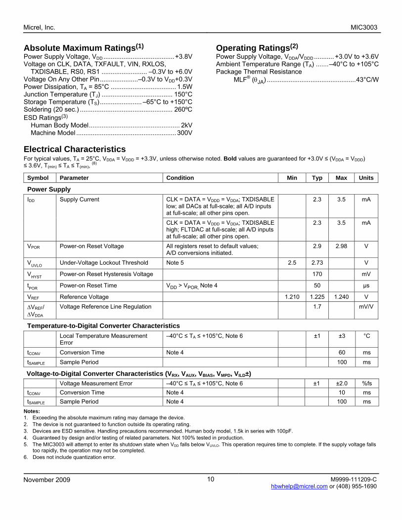
Absolute Maximum Ratings(1) Power Supply Voltage, VDD .......................................+3.8V Voltage on CLK, DATA, TXFAULT, VIN, RXLOS,
TXDISABLE, RS0, RS1 ......................... –0.3V to +6.0V Voltage On Any Other Pin.....................–0.3V to VDD+0.3V Power Dissipation, TA = 85°C .................................... 1.5W Junction Temperature (TJ) ....................................... 150°C Storage Temperature (TS)....................... –65°C to +150°C Soldering (20 sec.) ................................................... 260ºC ESD Ratings(3)
Human Body Model.................................................. 2kV Machine Model ....................................................... 300V
Operating Ratings(2) Power Supply Voltage, VDDA/VDDD ........... +3.0V to +3.6V Ambient Temperature Range (TA) .......–40°C to +105°C Package Thermal Resistance
MLF® (θJA) .................................................43°C/W
Electrical Characteristics For typical values, TA = 25°C, VDDA = VDDD = +3.3V, unless otherwise noted. Bold values are guaranteed for +3.0V ≤ (VDDA = VDDD) ≤ 3.6V, T(min) ≤ TA ≤ T(min), (8)
Symbol Parameter Condition Min Typ Max Units
Power Supply
CLK = DATA = VDDD = VDDA; TXDISABLE low; all DACs at full-scale; all A/D inputs at full-scale; all other pins open.
2.3 3.5 mA IDD Supply Current
CLK = DATA = VDDD = VDDA; TXDISABLE high; FLTDAC at full-scale; all A/D inputs at full-scale; all other pins open.
2.3 3.5 mA
VPOR Power-on Reset Voltage All registers reset to default values; A/D conversions initiated.
2.9 2.98 V
VUVLO Under-Voltage Lockout Threshold Note 5 2.5 2.73 V
VHYST Power-on Reset Hysteresis Voltage 170 mV
tPOR Power-on Reset Time VDD > VPOR, Note 4 50 µs
VREF Reference Voltage 1.210 1.225 1.240 V
ΔVREF/ ΔVDDA
Voltage Reference Line Regulation 1.7 mV/V
Temperature-to-Digital Converter Characteristics Local Temperature Measurement
Error –40°C ≤ TA ≤ +105°C, Note 6 ±1 ±3 °C
tCONV Conversion Time Note 4 60 ms tSAMPLE Sample Period 100 ms
Voltage-to-Digital Converter Characteristics (VRX, VAUX, VBIAS, VMPD, VILD±) Voltage Measurement Error –40°C ≤ TA ≤ +105°C, Note 6 ±1 ±2.0 %fs tCONV Conversion Time Note 4 10 ms tSAMPLE Sample Period Note 4 100 ms
Notes: 1. Exceeding the absolute maximum rating may damage the device. 2. The device is not guaranteed to function outside its operating rating. 3. Devices are ESD sensitive. Handling precautions recommended. Human body model, 1.5k in series with 100pF. 4. Guaranteed by design and/or testing of related parameters. Not 100% tested in production. 5. The MIC3003 will attempt to enter its shutdown state when VDD falls below VUVLO. This operation requires time to complete. If the supply voltage falls
too rapidly, the operation may not be completed. 6. Does not include quantization error.

Micrel, Inc. MIC3003
November 2009 11 [email protected] or (408) 955-1690
Voltage Input, VIN (Pin 14 used as an ADC Input) Symbol Parameter Condition Min Typ Max Units VIN Input Voltage Range –0.3 V ≤ VDD ≤ 3.6V GNDA 5.5 V
ILEAK Input Current VIN = VDD or GND; VAUX = VIN 55 µA
CIN Input Capacitance 10 pF
Digital-to-Voltage Converter Characteristics (VMOD, VBIAS) Accuracy –40°C ≤ TA ≤ +105°C, Note 7 ±1 2.0 %fs
tCONV Conversion Time Note 8 20 ms
DNL Differential Non-linearity Error Note 8 ±0.5 ±1 LSB
Bias Current Sense Inputs, VILD+, VILD– VILD Differential Input Signal Range,
| VILD+ – VILD
– | 0 VREF/4 mV
IIN+ VILD+ input current ±1 µA
VILD– referred to VDDA +150 µA IIN– VILD
– input current
| VILD+ – VILD
– | = 0.3V VILD– referred to GND -150 µA
CIN Input Capacitance 10 pF
APC Op Amp, FB, VBIAS, COMP GBW Gain Bandwidth Product CCOMP = 20pF; Gain = 1 1 MHz
TCVOS Input Offset Voltage Temperature Coefficient(4)
1 µV/°C
IOUT = 10mA, SRCE bit = 1 GNDA 1.25 V VOUT Output Voltage Swing
IOUT = -10mA, SRCE bit = 0 VDDA -1.25 VDDA V
ISC Output Short-Circuit Current 55 mA
tSC Short Circuit Withstand Time TJ ≤ 150°C, Note 8 sec
CCOMP = 20pF; gain = 1, to GND 55 dB PSRR Power Supply Rejection Ratio
CCOMP = 20pF; gain = 1, to VDD 40
AMIN Minimum Stable Gain CCOMP = 20pF, note 8 1 V/V
ΔV/Δt Slew Rate CCOMP = 20pF; gain = 1 3 V/µs
ΔRFB Internal Feedback Resistor Tolerance
±20 %
ΔRFB/Δt Internal Feedback Resistor Temperature Coefficient
25 ppm/C
START = 01h 0.375 mA
START = 02h 0.750 mA
START = 04h 1.500 mA
ISTART Laser Start-up Current Magnitude
START = 08h 3.000 mA
CIN Pin Capacitance 10 pF
Notes: 7. Does not include quantization error. 8. Guaranteed by design and/or testing of related parameters. Not 100% tested in production.

Micrel, Inc. MIC3003
November 2009 12 [email protected] or (408) 955-1690
Electrical Characteristics Symbol Parameter Condition Min Typ Max Units
VMOD Buffer Op-Amp, VMOD, VMOD– GBW Gain Bandwidth CCOMP = 20pF; gain = 1 1 MHz
TCVOS Input Offset Voltage Temperature Coefficient
1 µV/°C
IBIAS VMOD– Input Current ±0.1 ±1 µA
VOUT Output Voltage Swing IOUT = ±1mA GNDA+75 VDDA-75 mV
ISC Output Short-Circuit Current 35 mA
tSC Short Circuit Withstand Time TJ ≤ 150°C, Note 9 sec
CCOMP = 20pF; gain = 1, to GND 65 dB PSRR Power Supply Rejection Ratio
CCOMP = 20pF; gain = 1, to VDD 44 dB
AMIN Minimum Stable Gain CCOMP = 20pF 1 V/V
ΔV/ΔT Slew Rate CCOMP = 20pF; gain = 1 1 V/µs
CIN Pin Capacitance 10 pF
Control and Status I/O, TXDISABLE, TXFAULT, RS0, RRSOUT(GPO), SHDN(TXFIN), RXLOS(TRSOUT), /INT, RS1, QGPO VIL Low Input Voltage 0.8 V
VIH High Input Voltage 2.0 V
VOL Low Output Voltage IOL ≤ 3mA 0.3 V
VOH High Output Voltage (applies to SHDN only)
IOH ≤ 3mA VDDD–0.3 V
ILEAK Input Current ±1 µA
CIN Input Capacitance 10 pF
Transmit Optical Power Input, VMPD VIN Input Voltage Range Note 9 GNDA VDDA V
BIASREF=0 VREF V VRX Input Signal Range
BIASREF=1 VDDA–VREF VDDA V
CIN Input Capacitance Note 9 10 pF
ILEAK Input Current ±1 µA
Received Optical Power Input, VRX, RXPOT Input Voltage Range Note 9 GNDA VDDA V
VRX Valid Input Signal Range (ADC Input Range)
0 VREF V
RRXPOT(32) End-to-End Resistance RXPOT = 1Fh 32 KΩ
ΔRXPOT Resistor Tolerance ±20 % ΔRXPOT/ΔT Resistor Temperature Coefficient 25 ppm/ºC ΔVRX/VRXPOT Divider Ratio Accuracy 00 ≤ RXPOT ≤ 1Fh -5 +5 %
ILEAK Input Current RXPOT = 0 (disconnected) ±1 µA
CIN Input Capacitance Note 9 10 pF
ILEAK Input Current ±1 µA
Note: 9. Guaranteed by design and/or testing of related parameters. Not 100% tested in production.

Micrel, Inc. MIC3003
November 2009 13 [email protected] or (408) 955-1690
Electrical Characteristics Symbol Parameter Condition Min Typ Max Units
Control and Status I/O Timing, TXFAULT, TXDISABLE, RS0, RRSOUT, and RXLOS tOFF TXDISABLE Assert Time From input asserted to optical output
at 10% of nominal, CCOMP = 10nF. 10 µs
tON TXDISABLE De-assert Time From input de-asserted to optical output at 90% of nominal, CCOMP = 10nF.
1 ms
tINIT Initialization Time From power on or transmitter enabled to optical output at 90% of nominal and TX_FAULT de-asserted. Note 10
300 ms
tINIT2 Power-on Initialization Time From power on to APC loop-enabled. 200 ms
tFAULT TXFAULT Assert Time From fault condition to TXFAULT assertion. Note 10
95 µs
tRESET Fault Reset Time Length of time TXDISABLE must be asserted to reset fault condition.
10 µs
tLOSS_ON RXLOS Assert Time From loss of signal to RXLOS asserted. 95 µs
tLOSS_OFF RXLOS De-assert Time From signal acquisition to LOS de-asserted.
100 µs
tDATA Analog Parameter Data Ready From power on to valid analog parameter data available. Note 10
400 ms
tPROP_IN TXFAULT, TXDISABLE, RXLOS, RS0, RS1 Input Propagation Time
Time from input change to corresponding internal register bit set or cleared. Note 10
1 µs
tPROP_OUT TXFAULT, TRSOUT, TRRSOUT, /INT, QGPO Output Propagation Time
From an internal register bit set or cleared to corresponding output change. Note 10
1 µs
Fault Comparators FLTTMR Fault Suppression Timer Clock
Period Note 10 0.475 0.5 0.525 ms
Accuracy -3 +3 %/fs tREJECT Glitch Rejection Maximum length pulse that will not
cause output to change state. Note 10 4.5 µs
High level 95 %VDDA VSAT Saturation Detection Threshold Low level 5 %VDDA
Power-On Hour Meter Timebase Accuracy 0°C ≤ TA ≤ +70°, Note 10 +5 -5 % –40°C ≤ TA ≤ +105°C +10 -10 % Resolution Note 10 10 hours
Non-Volatile (FLASH) Memory
tWR Write Cycle Time, Note 11 Measured from the SMBus STOP condition of a one-byte to eight-byte write transaction. Note 10
13 ms
NVRAM Data Retention 100 years Endurance Maximum permitted number of write
cycles to any single NVRAM location 10,000 cycles
Notes: 10. Guaranteed by design and/or testing of related parameters. Not 100% tested in production. 11. The MIC3003 will not respond to serial bus transactions during an EEPROM write cycle. The host will receive a NACK response during tWR.

Micrel, Inc. MIC3003
November 2009 14 [email protected] or (408) 955-1690
Serial Data I/O Pin, Data Symbol Parameter Condition Min Typ Max Units
IOL = 3mA 0.4 V VOL Low Output Voltage IOL = 6mA 0.6 V
VIL Low Input Voltage 0.8 V VIH High Input Voltage 2.1 V ILEAK Input Current ±1 µA CIN Input Capacitance Note 12 10 pF
Serial Clock Input, CLK VIL Low Input Voltage 2.7V ≤ VDD ≤ 3.6V 0.8 V VIH High Input Voltage 2.7V ≤ VDD ≤ 3.6V 2.1 V ILEAK Input Current ±1 µA CIN Input Capacitance Note 12 10 pF
Serial Interface Timing(4) t1 CLK (clock) Period 2.5 µs t2 Data In Setup Time to CLK High 100 ns t3 Data Out Stable After CLK Low 300 ns t4 Data Low Setup Time to CLK Low Start Condition 100 ns t5 Data High Hold Time After CLK High Stop Condition 100 ns tDATA Data Ready Time From power on to completion of one set
of ADC conversions; analog data available via serial interface.
400 ms
QGPO Reset Pulse Timing t1 QGPO reset pulse low duration OEMCFG3 bit 7 = 1
A2h:255 (FFh) [2-0] switch to 111 112.5 125 137.5 µs
t2 QGPO reset de-assertion to the clearing of A2:FFh bits 2:0
OEMCFG3 bit 7 = 1 A2h:255 (FFh) [2-0] ≠ 111
20.25 22.5 24.75 ms
Note: 12. Guaranteed by design and/or testing of related parameters. Not 100% tested in production.
Serial Interface Timing Diagram
Serial Interface Timing

Micrel, Inc. MIC3003
November 2009 15 [email protected] or (408) 955-1690
Serial Interface Address Maps Address (Decimal)
Field Size (Bytes)
Name Description
0 –95 96 Serial ID defined by SFP MSA General-purpose NVRAM; R/W under valid OEM password. 96 – 127 32 Vendor Specific Vendor specific EEPROM 128 – 255 128 Reserved Reserved for future use. General-purpose NVRAM; R/W under
valid OEM password.
Table 1. MIC3003 Serial Interface Address Map, Device Address = A0h
Address(s) Hex Dec
Field Size (Bytes) Name Description
00-27 0-39 40 Alarm and Warning Thresholds High/low limits for warnings and alarms; writeable using the OEM password; read-only otherwise.
28-37 40-55 16 Reserved Reserved – do not write; reads undefined. 38-5B 56-91 36 Calibration Constants Numerical constants for external calibration; writeable using
the OEM password; read-only otherwise. 5C-5E 92-94 3 Reserved Reserved – do not write; reads undefined. 5F 95 1 Checksum General-purpose NVRAM; writeable using the OEM password;
read-only otherwise. 60-69 96-105 10 Analog Data Real time analog parameter data. 6A-6D 106-109 4 Reserved Reserved – do not write; reads undefined. 6E 110 1 Control/Status Register Control and status bits. 6F 111 1 Rate Select Control Bits [7-6] control the use of the RS0 and RS1 inputs and the
SRS0 and SRS1 register bits. 70-71 112-113 2 Alarm Flags Alarm status bits; read-only. 72-73 114-115 2 Reserved Reserved – do not write; reads undefined. 74-75 116-117 2 Warning Flags Warning status bits; read-only. 76 118 1 Extended Control/Status
Register Additional control and status bits.
77 119 1 Reserved Reserved – do not write; reads undefined. 78-7E 120-126 7 OEMPW OEM password entry field. The four-byte OEM password
location can be selected to be 78h-7Bh (120-123) by setting OEMCFG5 bit 2 to 0 (default) or 7Bh-7Eh (123-126) by setting OEMCFG5 bit 2 to a one.
7F 127 1 Vendor-specific Vendor specific. Reserved – do not write; reads undefined. 80-F7 128-247 120 User Scratchpad User-writeable EEPROM. General-purpose NVRAM. F8-F9 248-249 2 Alarms Masks Bit = 0: Corresponding alarm not masked.
Bit = 1: Corresponding alarm masked. FA-FB 250-251 2 Warnings Masks Bit = 0: Corresponding warning not masked.
Bit = 1: Corresponding warning masked. FC-FD 252-253 2 Reserved Reserved – do not write; reads undefined. FE 254 1 USRCTL End-user control and status bits. FF 255 1 RESETOUT Bits [2:0] of this register control the QGPO reset output (pin
17) If OEMCFG3 bit 7 is set to 1.
Table 2. MIC3003 Serial Interface Address Map, Device Address = A2

Micrel, Inc. MIC3003
November 2009 16 [email protected] or (408) 955-1690
Address(s) Hex Dec
Field Size (Bytes) Name Description
00-3F 0-63 64 BIASLUT1 First 64 entries of the bias current temperature compensation LUT (Look-up Table) The additional 12 entries are located in A6: 58h – 63h.
40-7F 64-127 64 MODLUT1 First 64 entries of the modulation current temperature compensation LUT. The additional 12 entries are located in A6:.64h – 6Fh.
80-BF 128-191 64 IFTLUT1 First 64 entries of the bias current fault threshold temperature compensation LUT. The additional 12 entries are located in A6: 70h - 7Bh.
C0-FF 192-255 64 HATLUT1 First 64 entries of the bias current high alarm threshold temperature compensation LUT. The additional 12 entries are located in A6: 7C-87h.
Table 3. MIC3003 Serial Interface Address Map (Temperature Compensation Tables), Device Address = A4h
Address(s) Hex Dec
Field Size (Bytes) Name Description
00 0 1 OEMCFG0 OEM configuration register 0 01 1 1 OEMCFG1 OEM configuration register 1 02 2 1 OEMCFG2 OEM configuration register 2 03 3 1 APCSET0 APC setpoint register 0 04 4 1 APCSET1 APC setpoint register 1 05 5 1 APCSET2 APC setpoint register 2 06 6 1 MODSET0 Modulation setpoint register 0 07 7 1 IBFLT Bias current fault-comparator threshold. This register is temperature
compensated. 08 8 1 TXPFLT TX power fault threshold 09 9 1 LOSFLT RX LOS fault-comparator threshold 0A 10 1 FLTTMR Fault comparator timer setting 0B 11 1 FLTMSK Fault source mask bits 0C-0F 12-15 4 OEMPWSET Password for access to OEM areas 10 16 1 OEMCAL0 OEM calibration register 0 11 17 1 OEMCAL1 OEM calibration register 1 12 18 1 LUTINDX Look-up table index read-back 13 19 1 OEMCFG3 OEM configuration register 3 14 20 1 APCDAC Reads back current APC DAC value (setpoint+offset) 15 21 1 MODDAC Reads back current modulation DAC value (setpoint+offset) 16 22 1 OEMREAD Reads back OEM calibration data 17 23 1 LOSFLTn LOS deassert threshold 18 24 1 RXPOT RXPOT tap selection 19 25 1 OEMCFG4 OEM configuration register 4 1A 26 1 OEMCFG5 OEM configuration register 5 1B 27 1 OEMCFG6 OEM configuration register 6 1C-1D 28-29 2 SCRATCH Reserved – do not write; reads undefined. 1E 30 1 MODSET 1 Modulation setpoint register 1

Micrel, Inc. MIC3003
November 2009 17 [email protected] or (408) 955-1690
Address(s)
HEX DEC Field Size (Bytes) Name Description
1F 31 1 MODSET 2 Modulation setpoint register 2 20-27 32-39 8 POHDATA Power-on hour meter scratchpad 28-47 40-71 32 RXLUT RX power internal calibration coefficient table. Eight sets of slope and
offset coefficients provide a piecewise-linear transfom for the receive power ADC result.
48-57 72-87 16 CALCOEF Slope and offset coefficients used for temperature, voltage, bias current, and transmit power internal calibration
58-63 88-99 12 IFTLUT2 Additional 12 entries of the bias current fault threshold temperature compensation LUT.
64-6F 100-111 12 BIASLUT2 Additional 12 entries of the bias current temperature compensation LUT. 70-7B 112-123 12 MODLUT2 Additional 12 entries of the modulation current temperature
compensation LUT. 7C-87 124-135 12 HATLUT2 Additional 12 entries of the bias current high alarm threshold
temperature compensation LUT. 88-CF 136-207 72 SCRATCH OEM scratchpad area D0-DD 208-221 14 RXLUTSEG/
SCRATCH Receive power calibration segment delimiters. Each of the eight segments can have its own slope and offset coefficient. Used to refine the shape of the piecewise-linear function used for receive power in internal calibration mode. These bytes may also be part of the OEM scratch pad if the hard coded delimiters option is selected, see the description of OEMCFG6
DE-FA 222-250 29 SCRATCH OEM scratchpad area FB-FC 251-252 2 POH Power on hour meter result; read-only FD 253 1 Data Ready Flags Data ready bits for each measured parameter; read-only FE 254 1 MFG_ID Manufacturer identification (Micrel’s manufacturer ID is 42, 2Ah) FF 255 1 DEV_ID Device ID and die revision
Table 4. MIC3003 Serial Interface Address Map (OEM Configuration Registers), Device Address = A6h

Micrel, Inc. MIC3003
November 2009 18 [email protected] or (408) 955-1690
Block Diagram
Figure 1. MIC3003 Block Diagram
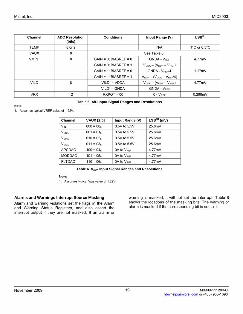
Analog-to-Digital Converter/Signal Monitoring A block diagram of the monitoring circuit is shown below. Each of the five analog parameters monitored by the MIC3003 is sampled in sequence. All five parameters are sampled and the results updated within the tCONV duration given in the “Electrical Characteristics” section. In OEM mode, the channel that is normally used to measure VIN may be assigned to measure the level of the VDDA pin or one of five other nodes. This provides a kind of analog loopback for debug and test purposes. The VAUX bits in OEMCFG0 control which voltage source is being sampled. The various VAUX channels are level-shifted differently depending on the signal source, resulting in different LSB values and signal ranges. See Table 5.
Figure 2. Analog-to-Digital Converter Block Diagram
Micrel, Inc. MIC3003
November 2009 19 [email protected] or (408) 955-1690
Channel ADC Resolution (bits)
Conditions Input Range (V) LSB(1)
TEMP 8 or 9 N/A 1°C or 0.5°C VAUX 8 See Table 6
GAIN = 0; BIASREF = 0 GNDA - VREF GAIN = 0; BIASREF = 1 VDDA – (VDDA – VREF)
4.77mV
GAIN = 1; BIASREF = 0 GNDA - VREF/4
VMPD 8
GAIN = 1; BIASREF = 1 VDDA – (VDDA – VREF/4) 1.17mV
VILD- = VDDA VDDA – (VDDA – VREF) VILD 8 VILD- = GNDA GNDA - VREF
4.77mV
VRX 12 RXPOT = 00 0 - VREF 0.298mV
Table 5. A/D Input Signal Ranges and Resolutions Note: 1. Assumes typical VREF value of 1.22V.
Channel VAUX [2:0] Input Range (V) LSB(1) (mV) VIN 000 = 00h 0.5V to 5.5V 25.6mV VDDA 001 = 01h 0.5V to 5.5V 25.6mV VBIAS 010 = 02h 0.5V to 5.5V 25.6mV VMOD 011 = 03h 0.5V to 5.5V 25.6mV APCDAC 100 = 04h 0V to VREF 4.77mV MODDAC 101 = 05h 0V to VREF 4.77mV FLTDAC 110 = 06h 0V to VREF 4.77mV
Table 6. VAUX Input Signal Ranges and Resolutions
Note: 1. Assumes typical VREF value of 1.22V.
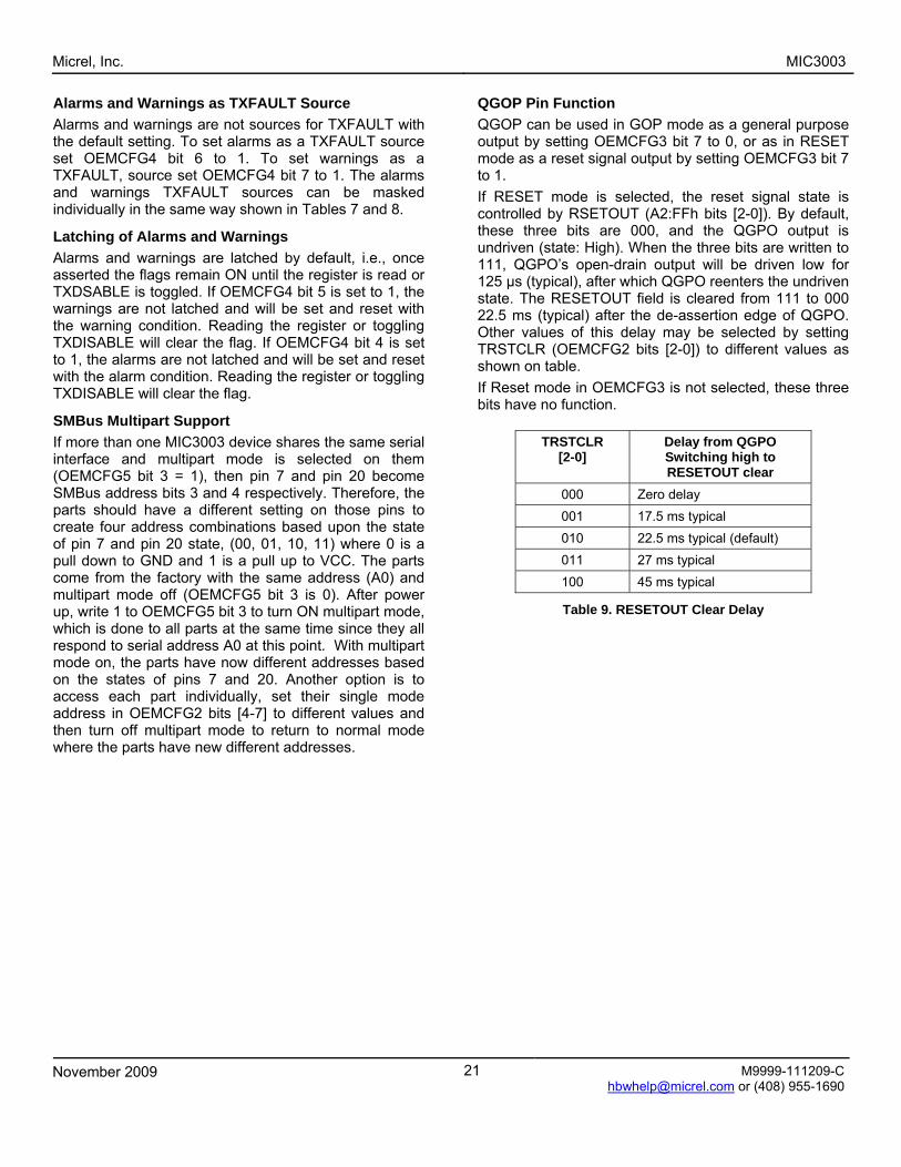
Alarms and Warnings Interrupt Source Masking Alarm and warning violations set the flags in the Alarm and Warning Status Registers, and also assert the interrupt output if they are not masked. If an alarm or
warning is masked, it will not set the interrupt. Table 8 shows the locations of the masking bits. The warning or alarm is masked if the corresponding bit is set to 1.

Micrel, Inc. MIC3003
November 2009 20 [email protected] or (408) 955-1690
Serial Address A2h Byte Bit Default Value Description
7 0 Masking bit for Temperature High Alarm interrupt source 6 0 Masking bit for Temperature Low Alarm interrupt source 5 0 Masking bit for Voltage High Alarm interrupt source 4 0 Masking bit for Voltage Low Alarm interrupt source 3 0 Masking bit for Bias High Alarm interrupt source 2 0 Masking bit for Bias Low Alarm interrupt source 1 0 Masking bit for TX Power High Alarm interrupt source
248
0 0 Masking bit for TX Power Low Alarm interrupt source 7 0 Masking bit for RX Power High Alarm interrupt source 6 1 Masking bit for RX Power Low Alarm interrupt source
249
[5-0] Reserved
Table 7. Alarms Interrupt Sources Masking Bits
Serial Address A2h Byte Bit Default Value Description
7 0 Masking bit for Temperature High Warning interrupt source
6 0 Masking bit for Temperature Low Warning interrupt source
5 0 Masking bit for Voltage High Warning interrupt source 4 0 Masking bit for Voltage Low Warning interrupt source 3 0 Masking bit for Bias High Warning interrupt source 2 0 Masking bit for Bias Low Warning interrupt source 1 0 Masking bit for TX Power High Warning interrupt source
250
0 0 Masking bit for TX Power Low Warning interrupt source 7 0 Masking bit for RX Power High Warning interrupt source 6 1 Masking bit for RX Power Low Warning interrupt source
251
[5-0] Reserved
Table 8. Warnings Interrupt Sources Masking Bits
Micrel, Inc. MIC3003
November 2009 21 [email protected] or (408) 955-1690
Alarms and Warnings as TXFAULT Source Alarms and warnings are not sources for TXFAULT with the default setting. To set alarms as a TXFAULT source set OEMCFG4 bit 6 to 1. To set warnings as a TXFAULT, source set OEMCFG4 bit 7 to 1. The alarms and warnings TXFAULT sources can be masked individually in the same way shown in Tables 7 and 8.
Latching of Alarms and Warnings Alarms and warnings are latched by default, i.e., once asserted the flags remain ON until the register is read or TXDSABLE is toggled. If OEMCFG4 bit 5 is set to 1, the warnings are not latched and will be set and reset with the warning condition. Reading the register or toggling TXDISABLE will clear the flag. If OEMCFG4 bit 4 is set to 1, the alarms are not latched and will be set and reset with the alarm condition. Reading the register or toggling TXDISABLE will clear the flag.
SMBus Multipart Support If more than one MIC3003 device shares the same serial interface and multipart mode is selected on them (OEMCFG5 bit 3 = 1), then pin 7 and pin 20 become SMBus address bits 3 and 4 respectively. Therefore, the parts should have a different setting on those pins to create four address combinations based upon the state of pin 7 and pin 20 state, (00, 01, 10, 11) where 0 is a pull down to GND and 1 is a pull up to VCC. The parts come from the factory with the same address (A0) and multipart mode off (OEMCFG5 bit 3 is 0). After power up, write 1 to OEMCFG5 bit 3 to turn ON multipart mode, which is done to all parts at the same time since they all respond to serial address A0 at this point. With multipart mode on, the parts have now different addresses based on the states of pins 7 and 20. Another option is to access each part individually, set their single mode address in OEMCFG2 bits [4-7] to different values and then turn off multipart mode to return to normal mode where the parts have new different addresses.
QGOP Pin Function QGOP can be used in GOP mode as a general purpose output by setting OEMCFG3 bit 7 to 0, or as in RESET mode as a reset signal output by setting OEMCFG3 bit 7 to 1. If RESET mode is selected, the reset signal state is controlled by RSETOUT (A2:FFh bits [2-0]). By default, these three bits are 000, and the QGPO output is undriven (state: High). When the three bits are written to 111, QGPO’s open-drain output will be driven low for 125 μs (typical), after which QGPO reenters the undriven state. The RESETOUT field is cleared from 111 to 000 22.5 ms (typical) after the de-assertion edge of QGPO. Other values of this delay may be selected by setting TRSTCLR (OEMCFG2 bits [2-0]) to different values as shown on table. If Reset mode in OEMCFG3 is not selected, these three bits have no function.
TRSTCLR [2-0]
Delay from QGPO Switching high to RESETOUT clear
000 Zero delay 001 17.5 ms typical 010 22.5 ms typical (default) 011 27 ms typical 100 45 ms typical
Table 9. RESETOUT Clear Delay

Micrel, Inc. MIC3003
November 2009 22 [email protected] or (408) 955-1690
Calibration Modes The default mode of calibration in the MIC3003 is external calibration, for which the INTCAL bit (bit 0 in OEMCFG3 register) is set to 0. The internal calibration mode is selected by setting INTCAL to 1.
A/ External Calibration The voltage and temperature values returned by the MIC3003’s A/D converter are internally calibrated. The binary values of TEMPh:TEMPl and VOLTh:VOLTl are in the format called for by SFF-8472 under Internal Calibration. SFF-8472 calls for a set of calibration constants to be stored by the transceiver OEM at specific non-volatile memory locations; refer to the SFF-8472 specifications for the memory map of the calibration coefficients. The MIC3003 provides the non-volatile memory required for the storage of these constants. The Digital Diagnostic Monitoring Interface specification should be consulted for full details. Slopes and offsets are stored for use with voltage, temperature, bias current, and transmitted power measurements. Coefficients for a fourth-order polynomial are provided for use with received power measurements. The host system can retrieve these constants and use them to process the measured data. Voltage The voltage values returned by the MIC3003’s A/D converter are internally calibrated. The binary values of VOLTh:VOLTl are in the format called for by SFF-8472 under Internal Calibration. Since VINh:VINl requires no processing, the corresponding slope should be set to one and the offset to zero. Temperature The temperature values returned by the MIC3003’s A/D converter are internally calibrated. The binary values of TEMPh:TEMPl are in the format called for by SFF-8472 under Internal Calibration. The temperature value may be offset by storing a value in A6:74(4Ah). The temperature offset is a six-bit signed quantity with .5 degrees C resolution. The temperature offset coefficient at A6:74(4Ah) is used in the same way in both internal and external calibration modes. Bias Current Bias current is sensed via an external sense resistor as a voltage appearing between VILD+ and VILD-. The value returned by the A/D is therefore a voltage analogous to bias current. Bias current, IBIAS, is simply VVILD/RSENSE. The binary value in IBIASh (IBIASl is always zero) is related to bias current by:
(1)
The value of the least significant bit (LSB) of IBIASh is given by: (2)
Per SFF-8472, the value of the bias current LSB is 2µA. The necessary conversion factor, “slope”, is therefore:
The tolerance of the sense resistor directly impacts the accuracy of the bias current measurement. It is recommended that the sense resistor chosen be 1% accurate or better. The offset correction, if needed, can be determined by shutting down the laser, i.e., asserting TXDISABLE, and measuring the bias current. Any non-zero result gives the offset required. The offset will be equal and opposite to the result of the “zero current” measurement. TX Power Transmit power is sensed via a resistor carrying the monitor photodiode current. In most applications, the signal at VMPD will be feedback voltage on FB. The VMPD voltage may be measured relative to GND or VDDA depending on the setting of the BIASREF bit in OEMCFG1. The value returned by the A/D is therefore a voltage analogous to transmit power. The binary value in TXOPh (TXOPl is always zero) is related to transmit power by: (3)
For a given implementation, the value of RSENSE is known. It is either the value of the external resistor or the selected internal value of RFB. The constant, K, will likely have to be determined through experimentation or closed-loop calibration, as it depends on the monitoring photodiode responsively and coupling efficiency. It should be noted that the APC circuit acts to hold the transmitted power constant. The value of transmit power reported by the circuit should only vary by a small amount as long as the APC is functioning correctly.

Micrel, Inc. MIC3003
November 2009 23 [email protected] or (408) 955-1690
RX Power Received power is sensed as a voltage appearing at VRX. It is assumed that this voltage is generated by a sense resistor carrying the receiver photodiode current or by the RSSI circuit of the receiver. The value returned by the A/D is therefore a voltage analogous to received power. The binary values in RXOPh and RXOPl are related to receive power by: RX(mW)=K x VREF x (256 x RXOPh +RXOPl/16)/ 65536 (4) For a given implementation, the constant, K, will likely have to be determined through experimentation or closed-loop calibration, as it depends upon the gain and efficiencies of the receiver. In SFF-8472 implementations, the external calibration constants can describe up to a fourth-order polynomial in case K is nonlinear.
B/ Internal Calibration If the INTCAL bit in OEMCFG3 is set to 1 (internal calibration selected), the MIC3003 will process each piece of data coming out of the A/D converter before storing the result in result register. Linear slope/offset correction will be applied on a per-channel basis to the measured values for voltage, bias current, TX power, and RX power. Only offset is applied to temperature. The user must store the appropriate slope/offset coefficients in memory at the time of transceiver calibration. In the case of RX power, a look-up table is provided that implements eight-segment piecewise-linear correction. This correction may be performed as a compensation of the receiver non-linearity over temperature or receive power level. If static slope/offset correction for RX power is desired, the eight coefficient sets can simply be made the same. The user has the option to select between using preset hard-coded delimiters values or programmable delimiters where delimiters corresponding to the best linear approximation intervals of a specific receiver can be entered. The latter option will use an additional fourteen (14) bytes from the OEM scratch pad A6h:208-221(DOh-DDh). OEMCFG6 bits [6:5] are used to select between these options. The memory maps for the calibration coefficients are shown in Tables 11 and 12. If the programmable delimiters option is selected, the user must enter the seven delimiters of the intervals that best fit the receiver response. The diagram in Figure 3 shows the link between the delimiters and the sets of slopes and offsets. Slopes Coefficients The slopes allow for the correction of gain errors. Each slope coefficient is an unsigned, sixteen-bit, fixed-point binary number in the format:
[mmmmmmmm.llllllll], (5)
where m is a data bit in the most-significant byte and l is a data bit in the least significant byte Slopes are always positive. The decimal point is in between the two bytes, i.e., between bits 7 and 8. This provides a numerical range of 1/256 (0.00391) to 255.997 in steps of 1/256. The most significant byte is always stored in memory at the lower numerical address. Offset coefficients The offsets correct for constant errors in the measured data. Each offset, apart from temperature, is a signed, sixteen-bit, fixed-point binary number. The bit-weights of the offsets are the same as that of the final results. The sixteen-bit offsets provide a numerical range of –32768 to +32767 for voltage, bias current, transmit power, and receive power.
The numerical range for the six-bit temperature offset is –32 (–16 °C) to +31 (+15.5 °C) in increments of .5 °C. The two most significant bits of the temperature offset coefficient are ignored by the MIC3003. Computing Internal Calibration Results Calibration of voltage, bias current, and TX power are performed using the following calculation: RESULTn = ADC_RESULTn x SLOPEn + OFFSETn (6) Calibration of RX power is performed using the following calculation: RESULT = ADC_RESULT x SLOPE(m) + OFFSET(m) (7) where m represents one of the eight linearization intervals corresponding to the RX power level. The results of these calculations are rounded to sixteen bits. If the seventeenth bit is a one, the result is rounded up to the next higher value. If the seventeenth bit is zero, the upper sixteen bits remain unchanged. The bit-weights of the offsets are the same as that of the final results. For SFF-8472 compatible applications, these bit-weights are given in Table 10.
Parameter Magnitude of LSB Voltage 100µV Bias Current 2µA TX Power 0.1µW RX Power 0.1µW
Table 10. LSB Values of Offset Coefficients

Micrel, Inc. MIC3003
November 2009 24 [email protected] or (408) 955-1690
Address(s)
HEX DEC Field Size Name Description
48-49 72-73 2 RESERVED Reserved. There is no slope for temperature. Do not write; reads undefined. 4A-4B 74-75 2 TOFFh:TOFFl Temperature offset; signed six-bit integer offset with an LSB resolution of .5
degrees C per bit. The two most significant bits of TOFFh are ignored. TOFFl is not used. Note that TOFFh is also used in external calibration mode.
4C-4D 76-77 2 VSLPh:VSLPl Voltage slope; unsigned fixed-point; MSB is at lower physical address. 4E-4F 78-79 2 VOFFh:VOFFl Voltage offset; signed integer; MSB is at lower physical address. 50-51 80-81 2 ISLPh:ISLPl Bias current slope; unsigned fixed-point; MSB is at lower physical address. 52-53 82-83 2 IOFFh:IOFFl Bias current offset; signed integer; MSB is at lower physical address. 54-55 84-85 2 TXSLPh: XSLPl TX power slope; unsigned fixed-point; MSB is at lower physical address. 56-57 86-87 2 TXOFFh: TXOFFl TX power slope; unsigned fixed-point; MSB is at lower physical address.
Table 11. Internal Calibration Coefficient Memory Map – Part I
Address(s) HEX DEC
Field Size Name Description
28-29 40-41 2 RXSLP0h: RXSLP0l RX power slope 0; unsigned fixed-point; MSB is at lower physical address. 2A-2B 42-43 2 RXOFF0h: RXOFF0l RX power offset 0; signed integer; MSB is at lower physical address. 2C-2D 44-45 2 RXSLP1h: RXSLP1l RX power slope 1; unsigned fixed-point; MSB is at lower physical address. 2E-2F 46-47 2 RXOFF1h: RXOFF1l RX power offset 1; signed integer; MSB is at lower physical address. 30-31 48-49 2 RXSLP2h: RXSLP2l RX power slope 2; unsigned fixed-point; MSB is at lower physical address. 32-33 50-51 2 RXOFF2h: RXOFF2l RX power offset 2; signed integer; MSB is at lower physical address. 34-35 52-53 2 RXSLP3h: RXSLP3l RX power slope 3; unsigned fixed-point; MSB is at lower physical address. 36-37 54-55 2 RXOFF3h: RXOFF3l RX power offset 3; signed integer; MSB is at lower physical address. 38-39 56-57 2 RXSLP4h: RXSLP4l RX power slope 4; unsigned fixed-point; MSB is at lower physical address. 3A-3B 58-59 2 RXOFF4h: RXOFF4l RX power offset 4; signed integer; MSB is at lower physical address. 3C-3D 60-61 2 RXSLP5h: RXSLP5l RX power slope 5; unsigned fixed-point; MSB is at lower physical address. 3E-3F 62-63 2 RXOFF5h: RXOFF5l RX power offset 5; signed integer; MSB is at lower physical address. 40-41 64-65 2 RXSLP6h: RXSLP6l RX power slope 6; unsigned fixed-point; MSB is at lower physical address. 42-43 66-67 2 RXOFF6h: RXOFF6l RX power offset 6; signed integer; MSB is at lower physical address. 44-45 68-69 2 RXSLP7h: RXSLP7l RX power slope 7; signed integer; MSB is at lower physical address. 46-47 70-71 2 RXOFF7h: RXOFF7l RX power offset 7; signed fixed-point; MSB is at lower physical address.
Table 12. Internal Calibration Coefficient Memory Map – Part II

Micrel, Inc. MIC3003
November 2009 25 [email protected] or (408) 955-1690
Figure 3. Internal Calibration RX Power Linear Approximation
C/ Reading the ADC Result Registers The ADC result registers should be read as 16-bit registers under internal calibration while under external calibration they should be read as 8-bit or 16-bit registers at the MSB address. For example, TX power should be read under internal calibration as 16 bits at address A2h: 66h–67h and under external calibration as 8 bits at address A2h: 66h. 9-bit temperature results and 12-bit receive power results should always be read as 16-bit quantities. Reading the result registers using two-byte burst reads on the SMBus guarantees that the two bytes are coherent with each other—that is, they form a matched result pair. If the two bytes were read separately, it is possible that the internal result could be updated between the reads, leading to an incorrect ADC result.
RXPOT A programmable, non-volatile digitally controlled potentiometer is provided for adjusting the gain of the receive power measurement signal chain in the analog domain. Five bits in the RXPOT register are used to set and adjust the position of potentiometer. RXPOT functions as a programmable divider or attenuator. It is adjustable in steps from 1:1 (no divider action) down to 1/32 in steps of 1/32. If RXPOT is set to zero, then the divider is bypassed completely. There will be no scaling of the input signal, and the resistor network will be disconnected from the VRX pin. At all other settings of RXPOT, there will be a 32kΩ (typical) load seen on VRX.
Figure 4. RXPOT Block Diagram
Laser Diode Bias Control The MIC3003 can be configured to generate a constant bias current using electrical feedback, or regulate average transmitted optical power using a feedback signal from a monitor photodiode, as shown in Figure 5. An operational amplifier is used to control laser bias current via the VBIAS output. The VBIAS pin can drive a maximum of ±10mA. An external bipolar transistor provides current gain. The polarity of the op amp’s output is programmable with BIASREF (bit-5 in OEMCFG1) in order to accommodate either NPN or PNP transistors that drive common anode and common cathode laser, respectively. Additionally, the polarity of the feedback signal is programmable for use with either common-emitter or emitter-follower transistor circuits.

Micrel, Inc. MIC3003
November 2009 26 [email protected] or (408) 955-1690
Furthermore, the reference level for the APC circuit is selectable to accommodate electrical, i.e., current feedback, or optical feedback via a monitor photodiode. Finally, any one of seven different internal feedback resistors can be selected. This internal resistor can be used alone or in parallel with an external resistor. This wide range of adjustability (50:1) accommodates a wide range of photodiode current, i.e., wide range of transmitter output power. The APC operating point can be kept near the mid-scale value of the APC DAC, insuring maximum SNR, maximum effective resolution for digital diagnostics, and the widest possible DAC adjustment range for temperature compensation, etc. See Figure 6. The APCCAL bit in OEMCAL0 is used to turn the APC function on and off. It will be turned on in the MIC3003’s default state as shipped from the factory. When the APC is on, the value in the selected APCSETx register is added to the signed compensation value taken from the APC look-up table and loaded into the VBIAS DAC. When the APC is off, the VBIAS DAC may be written directly via the VBIAS register, bypassing the look-up table entirely. This provides direct control of the laser diode bias during setup and calibration. In either case, the VBIAS DAC setting is reported in the APCDAC register.
Figure 5. MIC3003 APC and Modulation Control Block Diagram
Figure 6. Programmable Feedback Resistor
Laser Modulation Control As shown in Figure 5, a temperature-compensated DAC is provided to set and control the laser modulation current via an external laser driver circuit. The MODREF bit in OEMCFG0 selects whether the VMOD DAC output swings up from ground or down from VDD. If the laser driver requires a voltage input to set the modulation current, the MIC3003’s VMOD output can drive it directly. If a current input is required, a fixed resistor can be used between the driver and the VMOD output. Several different configurations are possible as shown in Figure 8. When the APC is on, i.e., the APCCAL bit in OEMCAL0 is set to 0, the value corresponding to the current temperature is taken from the MODLUT look-up table, added to the selected MODSETx register, and loaded into the VMOD DAC. When the APC is off, the compensation value in VMOD is loaded directly into the VMOD DAC, bypassing the look-up table entirely. This provides for direct modulation control for setup and calibration.
Figure 7. Transmitter Configurations Supported by MIC3003

Micrel, Inc. MIC3003
November 2009 27 [email protected] or (408) 955-1690
Figure 8. VMOD Configured as Voltage Output with Gain
Power On and Laser Start-Up When power is applied, the MIC3003 initializes its internal registers and state machine. This process takes tPOR, about 50ms. Following tPOR, analog-to-digital conversions begin, serial communication is possible, and the POR bit and data ready bits may be polled. The first set of analog data will be available tCONV after tPOR. MIC3003s are shipped from the factory with the output enable bit, OE, set to zero, off. The MIC3003’s power-up default state, therefore, is APC off, VBIAS, VMOD, and SHDN outputs disabled. VBIAS, VMOD, and SHDN will be floating (high impedance) and the laser diode, if connected, will be off. Once the device is incorporated into a transceiver and properly configured, then the shutdown states of SHDN, VBIAS, and VMOD will be determined by the state of the APC configuration and OE bits. Tables 13, 14, and 15 illustrate the shutdown states of the various laser control outputs versus the control bits.
Configuration Bits Shutdown State OE SPOL SHDN 0 Don’t Care Hi-Z 1 0 GND 1 1 VDD
Table 13. Shutdown State of SHDN vs. Configuration Bits
Configuration Bits VBIAS Shutdown State OE INV BIASREF VBIAS 0 Don’t Care Don’t Care Hi-Z 1 Don’t Care 0 GND 1 Don’t Care 1 VDD
Table 14. Shutdown State of VBIAS vs. Configuration Bits
Configuration Bits VMOD Shutdown State OE MODREF VMOD 0 Don’t Care Hi-Z 1 0 GND 1 1 VDD
Table 15. Shutdown State of VMOD vs. Configuration Bits
In order to facilitate hot-plugging, the laser diode is not turned on until tINIT2 after Power-On. Following tINIT2, and assuming TXDISABLE is not asserted, the DACs will be loaded with their initial values. Since tCONV is much less than tINIT2, the first set of analog data, including temperature, is available at tINIT2. Temperature compensation will be applied to the DAC values if enabled. APC will begin if OE is asserted. (If the output enable bit, OE, is not set, the VMOD, VBIAS, and SHDN outputs will float indefinitely.) Figure 9 shows the power-up timing of the MIC3003. If TXDISABLE is asserted at power-up, the VMOD and VBIAS outputs will stay in their shutdown states following MIC3003 initialization. A/D conversions will begin, but the laser will remain off.

Micrel, Inc. MIC3003
November 2009 28 [email protected] or (408) 955-1690
Figure 9. MIC3003 Power-On Timing (OE = 1)
Fault Comparators In addition to detecting and reporting the events specified in SFF-8472, the MIC3003 also monitors five fault conditions: inadequate supply voltage, thermal diode faults, excessive bias current, excessive transmit power, and APC op-amp saturation. Comparators monitor these parameters in order to respond quickly to fault conditions that could indicate link failure or safety issues, see Figure 10. When a fault is detected, the laser is shut down and TXFAULT is asserted. Each fault source may be independently disabled using the FLTMSK register. FLTMSK is non-volatile, allowing faults to be masked only during calibration and testing or permanently.
Figure 10. Fault Comparator Logic

Micrel, Inc. MIC3003
November 2009 29 [email protected] or (408) 955-1690
Thermal diode faults are detected within the temperature measurement subsystem when an out-of-range signal is detected. A window comparator circuit monitors the voltage on the compensation capacitor to detect APC op-amp saturation (Figure 11). Op-amp saturation indicates that some fault has occurred in the control loop such as loss of feedback. The saturation detector is blanked for a time, tFLTTMR, following laser turn-on since the compensation voltage will essentially be zero at turn-on. The FLTTMR interval is programmable from 0.5ms to 127.5ms (typical) in increments of 0.5ms (tFLTTMR). Note that a saturation comparator cannot be relied upon to meet certain eye-safety standards that require 100ms response times. This is because the operation of a saturation detector is limited by the loop bandwidth, i.e., the choice of CCOMP. Even if the comparator itself was very fast, it would be subject to the limited slew-rate of the APC op-amp. Only the other fault comparator channels will meet <100ms timing requirements. The MIC3003 can also except and respond to fault inputs from external devices. See the “SHDN and TXFIN” section. A similar comparator circuit monitors received signal strength and asserts RXLOS when loss-of-signal is detected (Figure 12). RXLOS will be asserted if VRX drops below the level programmed in LOSFLT. Hysteresis is implemented such that RXLOS will be de-asserted when VRX subsequently rises above the level programmed in LOSFLTn. The loss-of-signal comparator may be disabled completely by setting the LOSDIS bit in OEMCFG3. Once the LOS comparator is disabled, an external device may drive RXLOS. The state of the RXLOS pin is reported in the CNTRL register regardless of whether it is driven by the internal comparator or by an external device. A programmable digital-to-analog converter provides the comparator reference voltages for monitoring received signal strength, transmit power, and bias current. Since laser bias current varies greatly with temperature, there is a temperature compensation look-up table for the bias current fault DAC value. When a fault condition is detected, the laser will be shutdown immediately and TXFAULT will be asserted. The VMOD, VBIAS, and SHDN (if enabled by setting OEMCFG5 bit 7 to 1) outputs will be driven to their shutdown state according to the state of the configuration bits. The shutdown states of VMOD, VBIAS, and SHDN versus the configuration bit settings are shown in Table 12, Table 13, and Table 14.
SHDN and TXFIN SHDN and TXFIN are optional functions of pin 7. SHDN is an output function and is designed to drive a redundant safety switch in the laser current path. TXFIN is an input function and serves as an input for fault signals from external devices that must be reported to the host via
TXFAULT. The SHDN function is designed for applications in which the MIC3003 is performing all APC and laser management tasks. The TXFIN function is for situations in which an external device such as a laser diode driver IC is performing laser management tasks, including fault detection. If the TXFIN bit in OEMCFG3 is zero (the default mode), SHDN will be activated anytime the laser is off. Thus, it will be active if 1) TXDISABLE is asserted, 2) STXDIS in the CNTRL register, is set, or 3) a fault is detected. SHDN is a push-pull logic output. Its polarity is programmable via the SPOL bit in OEMCFG1. If TXFIN bit is set to one, pin 7 serves as an input that accepts fault signals from external devices such as laser diode driver ICs. Multiple TXFAULT signals cannot simply be wire-ORed together as they are open-drain and active high. The input polarity is programmable via the TXFPOL bit in OEMCFG3. TXFIN is logically ORed with the MIC3003’s internal fault sources to produce TXFAULT and determine the value of the transmit fault bit in CNTRL. See Figure 10.
Figure 11. Saturation Detector
Figure 12. RXLOS Comparator Logic

Micrel, Inc. MIC3003
November 2009 30 [email protected] or (408) 955-1690
Temperature Measurement The temperature-to-digital converter is built around a switched current source and an eight-bit/nine-bit analog-to-digital converter. The temperature is calculated by measuring the forward voltage of a diode junction at two different bias current levels. An internal multiplexer directs the current source’s output to a diode junction. This data is also used as the input to the temperature compensation look-up tables. Each time temperature is sampled and an updated value acquired, new corrective values for modulation current and the APC setpoint are read from the corresponding tables, added to the set values, and transferred to the DACs.
Diode Faults The MIC3003 is designed to respond in a failsafe manner to hardware faults in the temperature sensing circuitry. If there is a fault with the on-chip sensing diode, the temperature data reported by the A/D converter will be forced to its full-scale value (+127 °C). The diode fault flag, DFLT, will be set in OEMCFG0, TXFAULT will be asserted, and the high temperature alarm and warning flags will be set. The reported temperature will remain at +127 °C until the fault condition is cleared. Diode faults may be reset by toggling TXDISABLE, as with any other fault. Diode faults will not be detected at power up until the first A/D conversion cycle is completed.
Temperature Compensation Since the performance characteristics of laser diodes and photodiodes change with operating temperature, the MIC3003 provides a facility for temperature compensation of the APC. loop set-point, laser modulation current, bias current fault comparator threshold, and bias current high alarm flag threshold. Temperature compensation is performed using a look-up table (LUT) that stores values corresponding to each measured temperature over a 150°C span. Four identical tables reside at serial address A4h and A6h as summarized in Table 16. Each table entry is a signed twos complement integer that is used as an offset to the parameter being compensated. The default value of all table entries is zero, giving a flat response. The A/D converter reports a new temperature sample each tCONV. This occurs at roughly 10 Hz when 8-bit temperature resolution is selected. To prevent temperature oscillation due to thermal or electrical noise, sixteen successive temperature samples are averaged together and used to index the LUT.s. Temperature compensation results are therefore updated at 16xtCONV intervals, or about 1.6 seconds. This can be expressed as shown in Equation 8:
(8) Each time an updated average value is acquired, a new offset value for the APC setpoint is read from the corresponding look-up table (see Table 17) and transferred to the APC circuitry. This is illustrated in Equation 11. In a same way, new offset values are taken from similar look-up tables (see Table 18 and Table 19), added to the nominal values and transferred into the modulation and fault comparator DACs. The bias current high alarm threshold is compensated using a fourth look-up table (see Table 20). This compensation happens internally and does not affect any host-accessible registers.
(9) If the measured temperature is greater than the maximum table value, the highest value in each table is used. If the measured temperature is less than the minimum, the minimum value is used. Hysteresis is employed to further enhance noise immunity and prevent oscillation. Each table entry spans two degrees C. The table index will not change unless the new temperature average results in a table index beyond the midpoint of the next entry in either direction. There is therefore 2 to 3°C of hysteresis on temperature compensation changes. The table index will never oscillate due to quantization noise as the hysteresis is much larger than ±1⁄2 LSB.
Serial Address
Byte Addresses
Function
00h–3Fh APC Look-up Table 40h–7Fh IMOD Look-up Table 80h–BFh IFLT Look-up Table
Base address +4h
C0h–FFh Bias High Alarm Look-up Table 58h–63h APC Look-up Table (cont.) 64h–6Fh IMOD Look-up Table (cont.) 70h–7Bh IFLT Look-up Table (cont.)
Base address +6h
7Ch–87h Bias High Alarm Look-up Table (cont.)
Table 16. Temperature Compensation Look-up Tables

Micrel, Inc. MIC3003
November 2009 31 [email protected] or (408) 955-1690
Serial Address Register Address
Table Offset
Temperature Offset (°C)
00h 0 ≤ -45
-44 01h 1 -43
• • •
• • •
• • •
80
Base address +4h
3Fh 63 81 82 64h 64 83
• •
• •
• •
102 6E 74 103
Base address +6h
6F 75 ≥ 104 Table 17. APC Temperature Compensation
Look-Up Table
Serial Address Register Address
Table Offset
Temperature Offset (°C)
40h 0 ≤ -45
-44 41h 1 -43
• • •
• • •
• • •
80
Base address +4h
7Fh 63 81 82 70 64 83
• •
• •
• •
102 7A 74 103
Base address +6h
7B 75 ≥ 104 Table 18. IMOD Temperature Compensation
Look-Up Table
Serial Address Register Address
Table Offset
Temperature Offset (°C)
80h ≤ -45
-44 81h -43 82h
• • •
• • •
• • • BEh 80
Base address +4h
BFh 63 81 82 58 64 83
• •
• •
• •
102 62 74 103
Base address +6h
63 75 ≥ 104 Table 19. IBIAS Comparator Temperature Compensation
Look-Up Table
Serial Address Register Address
Table Offset
Temperature Offset (°C)
C0h ≤ -45
-44 C1h -43 C2h
• • •
• • •
• • • FEh 80
Base address +4h
FFh 63 81 82 7C 64 83
• •
• •
• •
87 74 102
Base address +6h
103 Table 20. BIAS Current High Alarm Temperature
Compensation Table

Micrel, Inc. MIC3003
November 2009 32 [email protected] or (408) 955-1690
The internal state machine calculates a new table index each time a new average temperature value becomes available. This table index is derived from the average temperature value. The table index is then converted into a table address for each of the four look-up tables. These operations can be expressed as:
(10)
where TAVG(n) is the current average temperature; and
TABLE_ADDRESS=INDEX+BASE_ADDRESS
where BASE_ADDRESS is the physical base address of each table, i.e., 00h, 20h, 40h, 80h, or 60h (tables reside in the Base address + 4h and Base address + 6h pages of memory). At any given time, the current table index can be read in the LUTINDX register. Alarms and Warning Flags There are 20 different conditions that will cause the MIC3003 to set one of the bits in the WARNx or ALARMx registers. These conditions are listed in Table 21. The less critical of these events generate warning flags by setting a bit in WARN0 or WARN1. The more critical events cause bits to be set in ALARM0 or ALARM1. An event occurs when any alarm or warning condition becomes true. Each event causes its corresponding status bit in ALARM0, ALARM1, WARN0, or WARN1 to be set. This action cannot be masked by the host. IF OEMCFG-4 bits [7-4] are set to 0 (default value), the status bit will remain set until the host reads that particular status register, a power on-off cycle occurs, or the host toggles TXDISABLE. If TXDISABLE is asserted at any time during normal operation, A/D conversions continue. The A/D results for all parameters will continue to be reported. All events will be reported in the normal way. If they have not already been individually cleared by read operations, when TXDISABLE is deasserted, all status registers will be cleared.
Control and Status I/O The logic for the transceiver control and status I/O is shown schematically in Figure 13. Note that the internal drivers on RXLOS/TRSOUT, RRSOUT/GPO, QGPO, and TXFAULT are all open-drain. These signals may be driven either by the internal logic or external drivers connected to the corresponding MIC3003 pins. In any case, the signal level appearing at the pins of the MIC3003 will be reported in the control register status bits. Note that the control bits for TX_DISABLE and RRSOUT, TRSOUT, and the status bits for TXFAULT and RXLOS do not meet the timing requirements as specified in the SFP MSA or the GBIC Specification, revision 5.5 (SFF-8053) for the hardware signals. The speed of the SMBus serial interface limits the rate at which these functions can be manipulated and/or reported. The response time for the control and status bits is given in the “Electrical Characteristics” subsection.
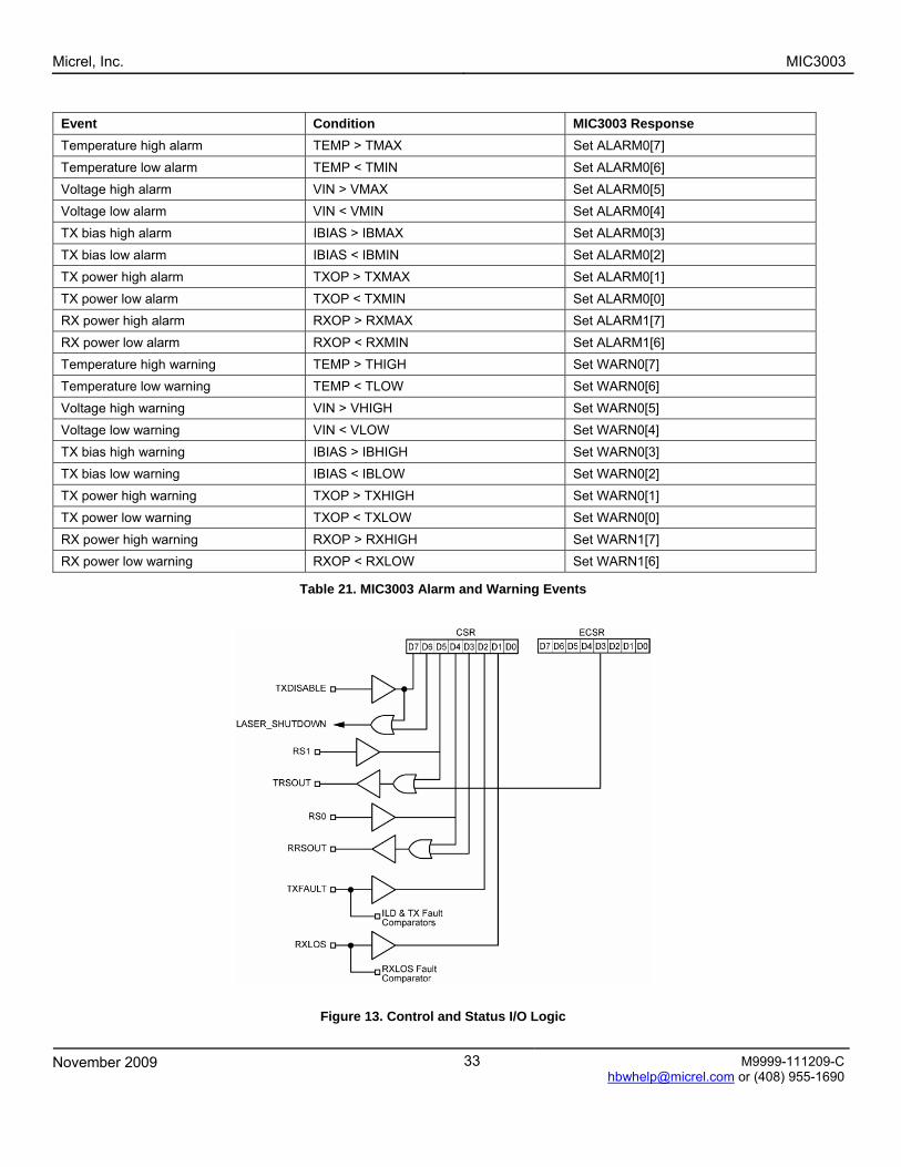
Micrel, Inc. MIC3003
November 2009 33 [email protected] or (408) 955-1690
Event Condition MIC3003 Response Temperature high alarm TEMP > TMAX Set ALARM0[7] Temperature low alarm TEMP < TMIN Set ALARM0[6] Voltage high alarm VIN > VMAX Set ALARM0[5] Voltage low alarm VIN < VMIN Set ALARM0[4] TX bias high alarm IBIAS > IBMAX Set ALARM0[3] TX bias low alarm IBIAS < IBMIN Set ALARM0[2] TX power high alarm TXOP > TXMAX Set ALARM0[1] TX power low alarm TXOP < TXMIN Set ALARM0[0] RX power high alarm RXOP > RXMAX Set ALARM1[7] RX power low alarm RXOP < RXMIN Set ALARM1[6] Temperature high warning TEMP > THIGH Set WARN0[7] Temperature low warning TEMP < TLOW Set WARN0[6] Voltage high warning VIN > VHIGH Set WARN0[5] Voltage low warning VIN < VLOW Set WARN0[4] TX bias high warning IBIAS > IBHIGH Set WARN0[3] TX bias low warning IBIAS < IBLOW Set WARN0[2] TX power high warning TXOP > TXHIGH Set WARN0[1] TX power low warning TXOP < TXLOW Set WARN0[0] RX power high warning RXOP > RXHIGH Set WARN1[7] RX power low warning RXOP < RXLOW Set WARN1[6]
Table 21. MIC3003 Alarm and Warning Events
Figure 13. Control and Status I/O Logic

Micrel, Inc. MIC3003
November 2009 34 [email protected] or (408) 955-1690
System Timing The timing specifications for MIC3003 control and status I/O are given in the “Electrical Characteristics” subsection.
Figure 14. Transmitter On-Off Timing
Figure 15. Initialization Timing with TXDISABLE Asserted
Figure 16. Initialization Timing with TXDISABLE Not Asserted

Micrel, Inc. MIC3003
November 2009 35 [email protected] or (408) 955-1690
Figure 17. Loss-of-Signal (LOS) Timing
Figure 18. Transmit Fault Timing

Micrel, Inc. MIC3003
November 2009 36 [email protected] or (408) 955-1690
Figure 19. Successfully Clearing a Fault Condition
Figure 20. Unsuccessful Attempt to Clear a Fault
Warm Resets The MIC3003 can be reset to its power-on default state during operation by setting the RST bit in OEMCFG0. When this bit is set, TXFAULT and RXLOS will be de-asserted, all registers will be restored to their normal power-on default values, and any A/D conversion in progress will be halted and the results discarded. The state of the MIC3003 following this operation is indistinguishable from a power-on reset.
Power-On Hour Meter The Power-On Hour meter logs operating hours using an internal real-time clock and stores the result in NVRAM. The hour count is incremented at ten-hour intervals in the middle of each interval. The first increment therefore takes place five hours after power-on. Time is accumulated whenever the MIC3003 is powered. The hour meter’s time base is accurate to +/-10% over all MIC3003 operating conditions, and is accurate to +/-5% in the range 0 to 70 degrees C. The counter is capable of storing counts of more than thirty years, but is ultimately limited by the write-cycle endurance of the non-volatile
memory. This implies a range of at least twenty years. Actual results will depend upon the operating conditions and write-cycle endurance of the part in question. Two registers, POHh and POHl, contain a 15-bit power-on hour measurement and an error flag, POHFLT. Great care has been taken to make the MIC3003’s hour meter immune to data corruption and to insure that valid data is maintained across power cycles. The hour meter employs multiple data copies and error correction codes to maintain data validity. This data is stored in the POHDATA registers. If POHFLT is set, however, the power-on hour meter data has been corrupted and should be ignored. It is recommended that a two-byte sequential read operation be performed on POHh and POHl to insure coherency between the two registers. These registers are accessible by the OEM using a valid OEM password. The only operation that should be performed on these registers is to clear the hour meters initial value, if necessary, at the time of product shipment. The hour meter result may be cleared by setting all eight POHDATA bytes to 00h.

Micrel, Inc. MIC3003
November 2009 37 [email protected] or (408) 955-1690
Test and Calibration Features Numerous features are included in the MIC3003 to facilitate development, testing, and diagnostics. These
features are available via registers in the OEM area. As shown in Table 22, these features include:
Function
Description
Control Register(s)
Analog loop-back Provides analog visibility of op-amp and DAC outputs via the ADC OEMCFG0 Fault comparator disable control Disables the fault comparator OEMCAL0 Fault comparator spin-on-channel mode
Selects a single fault comparator channel OEMCAL0
Fault comparator output read-back Allows host to read individual fault comparator outputs OEMRD TRSOUT, /INT read-back Allows host to read the state of these pins OEMRD Inhibit EEPROM write cycles Speeds repetitive writes to registers backed up by NVRAM OEMCAL0 APC calibration mode Allows direct writes to MODDAC and APCDAC (temperature
compensation not used) OEMCAL0
Continuity checking Forcing of RXLOS, TXFAULT, /INT OEMCAL0 Halt A/D Stops A/D conversions; ADC in one-shot mode OEMCAL1 ADC idle flag Indicates ADC status OEMCAL1 A/D one-shot mode Performs a single A/D conversion on the selected input channel OEMCAL1 A/D spin-on-channel mode Selects a single input channel OEMCAL1 Channel selection Selects ADC or fault comparator channel for spin-on-channel
modes OEMCAL1
LUT index read-back Permits visibility of the LUT index calculated by the state-machine LUTINDX Manufacturer and device ID registers Facilitates presence detection and version control MFG_ID,
DEV_ID
Table 22. Test and Diagnostic Features

Micrel, Inc. MIC3003
November 2009 38 [email protected] or (408) 955-1690
Serial Port Operation The MIC3003 uses standard write byte, read byte, and read word operations for communication with its host. It also supports block write and block read transactions. The write byte operation involves sending the devices address (with the R/W bit low to signal a write operation), followed by the address of the register to be operated upon and the data byte. The read byte operation is a composite write and read operation: the host first sends the devices address followed by the register address, as in a write operation. A new start bit must then be sent to the MIC3003, followed by a repeat of the device address with the R/W bit (LSB) set to the high (read) state. The data to be read from the part may then be clocked out. A read word is similar, but two successive data bytes are clocked out rather than one. These protocols are shown in Figures 21 to 24. The MIC3003 will respond to up to four sequential device addresses depending upon whether it is in OEM or User mode. A match between one of the MIC3003’s addresses and the address specified in the serial bit stream must be made to initiate communication. The MIC3003 responds to device addresses A0h and A2h in User Mode; it also responds to A4h and A6h in OEM Mode (assuming the base address is A0h).
Block Writes To increase the speed of block writes, the MIC3003 allows up to eight consecutive bytes to be written before the internal memory update begins. The block write sequence begins just like a write byte operation with the host sending the device address, R/W bit low, register address, etc. After the first data byte is sent the host will receive an acknowledge. Up to seven more bytes can be sent in sequence. The MIC3003 will acknowledge each one and increment its internal address register in anticipation of the next byte. After the last byte is sent, the host issues a STOP. The MIC3003’s internal write process then begins. Block writes of up to eight bytes can begin and end at any byte address without restriction. Block writes that increment over register address FFh will simply “wrap around” and continue at address 00h within the same device address space. To accelerate calibration and testing, NVRAM write cycles can be disabled completely by setting the WRINH bit in OEMCAL0. Writes to registers that do not have NVRAM backup, will not incur write-cycle delays when writes are inhibited. Write operations on registers that exist only in NVRAM will still incur write cycle delays.
Figure 21. Write Byte Protocol
Figure 22. Read Byte Protocol
Figure 23. Read_Word Protocol
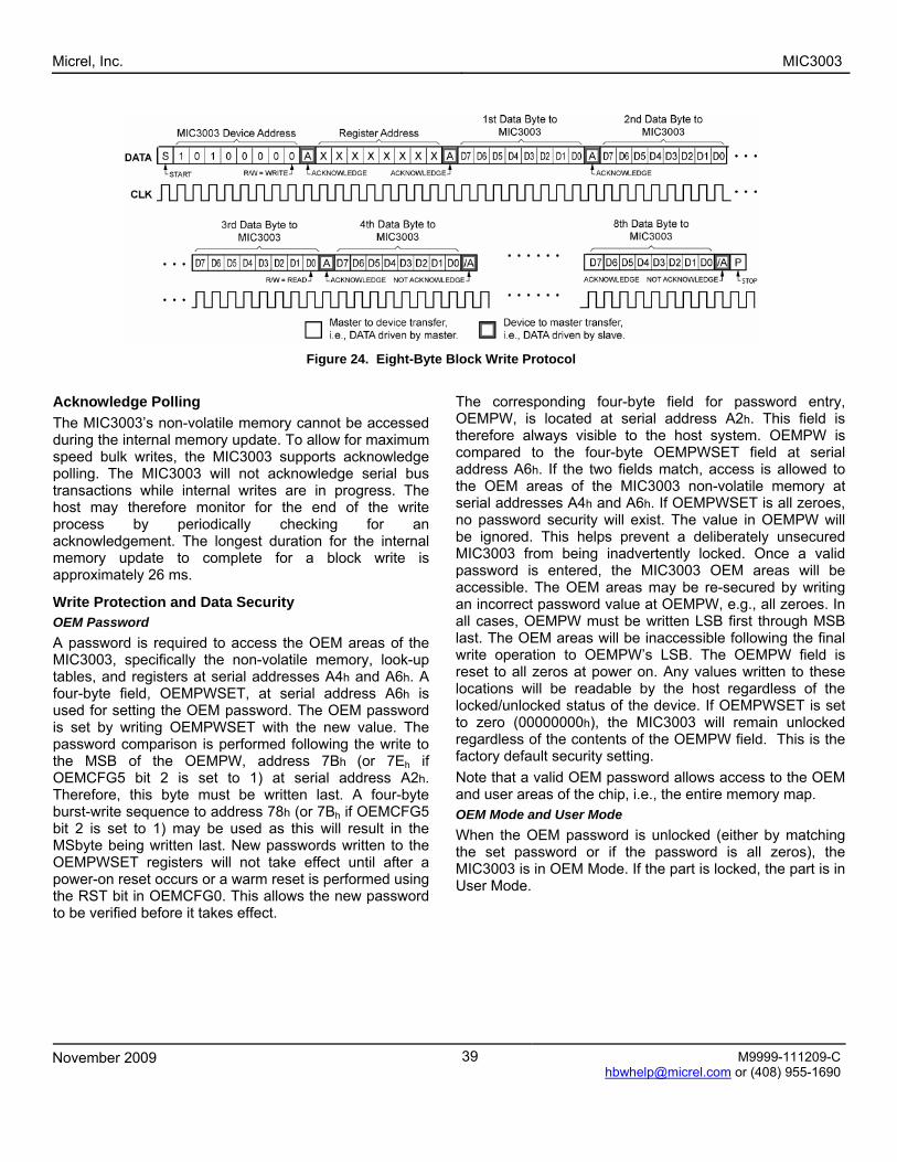
Micrel, Inc. MIC3003
November 2009 39 [email protected] or (408) 955-1690
Figure 24. Eight-Byte Block Write Protocol
Acknowledge Polling The MIC3003’s non-volatile memory cannot be accessed during the internal memory update. To allow for maximum speed bulk writes, the MIC3003 supports acknowledge polling. The MIC3003 will not acknowledge serial bus transactions while internal writes are in progress. The host may therefore monitor for the end of the write process by periodically checking for an acknowledgement. The longest duration for the internal memory update to complete for a block write is approximately 26 ms.
Write Protection and Data Security OEM Password A password is required to access the OEM areas of the MIC3003, specifically the non-volatile memory, look-up tables, and registers at serial addresses A4h and A6h. A four-byte field, OEMPWSET, at serial address A6h is used for setting the OEM password. The OEM password is set by writing OEMPWSET with the new value. The password comparison is performed following the write to the MSB of the OEMPW, address 7Bh (or 7Eh if OEMCFG5 bit 2 is set to 1) at serial address A2h. Therefore, this byte must be written last. A four-byte burst-write sequence to address 78h (or 7Bh if OEMCFG5 bit 2 is set to 1) may be used as this will result in the MSbyte being written last. New passwords written to the OEMPWSET registers will not take effect until after a power-on reset occurs or a warm reset is performed using the RST bit in OEMCFG0. This allows the new password to be verified before it takes effect.
The corresponding four-byte field for password entry, OEMPW, is located at serial address A2h. This field is therefore always visible to the host system. OEMPW is compared to the four-byte OEMPWSET field at serial address A6h. If the two fields match, access is allowed to the OEM areas of the MIC3003 non-volatile memory at serial addresses A4h and A6h. If OEMPWSET is all zeroes, no password security will exist. The value in OEMPW will be ignored. This helps prevent a deliberately unsecured MIC3003 from being inadvertently locked. Once a valid password is entered, the MIC3003 OEM areas will be accessible. The OEM areas may be re-secured by writing an incorrect password value at OEMPW, e.g., all zeroes. In all cases, OEMPW must be written LSB first through MSB last. The OEM areas will be inaccessible following the final write operation to OEMPW’s LSB. The OEMPW field is reset to all zeros at power on. Any values written to these locations will be readable by the host regardless of the locked/unlocked status of the device. If OEMPWSET is set to zero (00000000h), the MIC3003 will remain unlocked regardless of the contents of the OEMPW field. This is the factory default security setting. Note that a valid OEM password allows access to the OEM and user areas of the chip, i.e., the entire memory map. OEM Mode and User Mode When the OEM password is unlocked (either by matching the set password or if the password is all zeros), the MIC3003 is in OEM Mode. If the part is locked, the part is in User Mode.

Micrel, Inc. MIC3003
November 2009 40 [email protected] or (408) 955-1690
Detailed Register Descriptions Note: Serial bus addresses shown assume that the base device address is AOh.
Alarm Threshold Registers Temperature High Alarm Threshold
D[7] read/write
D[6] read/write
D[5] read/write
D[4] read/write
D[3] read/write
D[2] read/write
D[1] read/write
D[0] read/write
Default value for both bytes 0000 0000b = 00h (0 °C)
Serial address A2h Byte addresses MS byte (TMAXh): 00 = 00h
LS byte (TMAXl): 01 = 01h
Each LS bit of TMAXh represents one degree Celsius. TMAXl is not used, since all limit comparisons for temperature use eight-bit values. The eight bits of the high alarm threshold value (TMAXh) are compared to the temperature result (TEMPh). ALARM0 bit 7 is set if Result > Threshold.
Temperature Low Alarm Threshold D[7]
read/write D[6]
read/write D[5]
read/write D[4]
read/write D[3]
read/write D[2]
read/write D[1]
read/write D[0]
read/write Default value for both bytes 0000 0000b = 00h (0 °C)
Serial address A2h
Byte addresses MS byte (TMINh): 02 = 02h LS byte (TMINl): 03 = 03h
Each LS bit of TMINh represents one degree Celsius. TMINl is not used, since all limit comparisons for temperature use eight-bit values.. The eight MS bits of the low alarm threshold value (TMINh) are compared to the temperature result (TEMPh). ALARM0 bit 6 is set if Result < Threshold.
Voltage High Alarm Threshold D[7]
read/write D[6]
read/write D[5]
read/write D[4]
read/write D[3]
read/write D[2]
read/write D[1]
read/write D[0]
read/write Default value for both bytes 0000 0000b = 00h (0 V)
Serial address A2h
Byte addresses MS byte (VMAXh): 08 = 08h LS byte (VMAXl): 09 = 09h
Each LS bit of VMAXh represents 25.6 mV and each LS bit of VMAXl represents 0.1 mV. The sixteen-bit threshold value (VMAXh:VMAXl) is compared to the sixteen bits value of the voltage result (VINh:VINl). ALARM0 bit 5 is set if Result > Threshold.

Micrel, Inc. MIC3003
November 2009 41 [email protected] or (408) 955-1690
Voltage Low Alarm Threshold D[7]
read/write D[6]
read/write D[5]
read/write D[4]
read/write D[3]
read/write D[2]
read/write D[1]
read/write D[0]
read/write Default value for both bytes 0000 0000b = 00h (0 V)
Serial address A2h
Byte addresses MS byte (VMINh): 10 = 0Ah LS byte (VMINl): 11 = 0Bh
Each LS bit of VMINh represents 25.6 mV and each LS bit of VMINl represents 0.1 mV. The sixteen-bit threshold value (VMINh:VMINl) is compared to the sixteen-bit value of the voltage result (VINh:VINl). ALARM0 bit 4 is set if Result < Threshold.
Bias Current High Alarm Threshold D[7]
read/write D[6]
read/write D[5]
read/write D[4]
read/write D[3]
read/write D[2]
read/write D[1]
read/write D[0]
read/write Default value for both bytes 0000 0000b = 00h (0 mA)
Serial address A2h
Byte addresses MS byte (IMAXh): 16 = 10h LS byte (IMAXl): 17 = 11h
Each LS bit of IMAXh represents 512 μA and each LS bit of IMAXl represents 2 μA. The sixteen-bit threshold value (IMAXh:IMAXl) is compared,to the sixteen-bit value of the bias current result (ILDh:ILDl). ALARM0 bit 3 is set if Result > Threshold.
Bias Current Low Alarm Threshold D[7]
read/write D[6]
read/write D[5]
read/write D[4]
read/write D[3]
read/write D[2]
read/write D[1]
read/write D[0]
read/write Default value for both bytes 0000 0000b = 00h (0 mA)
Serial address A2h
Byte addresses MS byte (IMINh): 18 = 12h LS byte (IMINl): 19 = 13h
Each LS bit of IMINh represents 512 μA and each LS bit of IMINl represents 2 μA. The sixteen-bit threshold value (IMINh:IMINl) is compared to the sixteen-bit value of the bias current result (ILDh:ILDl). ALARM0 bit 2 is set if Result < Threshold.
TX Optical Power High Alarm Threshold D[7]
read/write D[6]
read/write D[5]
read/write D[4]
read/write D[3]
read/write D[2]
read/write D[1]
read/write D[0]
read/write Default value for both bytes 0000 0000b = 00h (0 mW)
Serial address A2h
Byte addresses MS byte (TXMAXh): 24 = 18h LS byte (TXMAXl): 25 = 19h
Each LS bit of TXMAXh represents 25.6 μW, and each LS bit of TXMAXl represents 0.1 μW. The sixteen-bit threshold value (TXMAXh:TXMAXl) is compared to the sixteen-bit value of the TX power result (TXOPh:TXOPl). ALARM0 bit 1 is set if Result > Threshold.

Micrel, Inc. MIC3003
November 2009 42 [email protected] or (408) 955-1690
TX Optical Power Low Alarm Threshold D[7]
read/write D[6]
read/write D[5]
read/write D[4]
read/write D[3]
read/write D[2]
read/write D[1]
read/write D[0]
read/write Default value for both bytes 0000 0000b = 00h (0 mW)
Serial address A2h
Byte addresses MS byte (TXMINh): 26 = 1Ah LS byte (TXMINl): 27 = 1Bh
Each LS bit of TXMINh represents 25.6 μW, and each LS bit of TXMINl represents 0.1 μW. The sixteen-bit threshold value (TXMINh:TXMINl) is compared,to the sixteen-bit value of the TX power reading (TXOPh:TXOPl). ALARM0 bit 0 is set if Result < Threshold.
RX Optical Power High Alarm Threshold D[7]
read/write D[6]
read/write D[5]
read/write D[4]
read/write D[3]
read/write D[2]
read/write D[1]
read/write D[0]
read/write Default value for both bytes 0000 0000b = 00h (0 mW)
Serial address A2h
Bytes addresses MS byte (RXMAXh): 32 = 20h LS byte (RXMAXl): 33 = 21h
Each LS bit of RXMAXh represents 25.6 μW, and each LS bit of RXMAXl represents 0.1 μW. The sixteen-bit threshold value (RXMAXh:RXMAXl) is compared to the sixteen-bit value of the RX power result (RXOPh:RXOPl). ALARM1 bit 7 is set if Result > Threshold.
RX Optical Power Low Alarm Threshold D[7]
read/write D[6]
read/write D[5]
read/write D[4]
read/write D[3]
read/write D[2]
read/write D[1]
read/write D[0]
read/write Default value for both bytes 0000 0000b = 00h (0mW)
Serial Address A2h
Byte Address MS byte (RXMINh): 34 = 22h LS byte (RXMINl): 35 = 23h
Each LSB of RXMINh represents 25.6 μW, and each LS bit of RXMINl represents 0.1 μW. The sixteen-bit threshold value (RXMINh:RXMINl) is compared to the sixteen-bit value of the RX power result (RXOPh:RXOPl). ALARM1 bit 6 is set if Result < Threshold.

Micrel, Inc. MIC3003
November 2009 43 [email protected] or (408) 955-1690
Warning Threshold Registers Temperature High Warning Threshold
D[7] read/write
D[6] read/write
D[5] read/write
D[4] read/write
D[3] read/write
D[2] read/write
D[1] read/write
D[0] read/write
Default value for both bytes 0000 0000b = 00h (0 °C)
Serial address A2h
Bytes addresses MS byte (THIGHh): 04 = 04h LS byte (THIGHl): 05 = 05h
Each LS bit of THIGHh represents one degree Celsius. THIGHl is not used, since all limit comparisons for temperature use eight-bit values. The eight bits of the high warning threshold value (THIGHh) are compared to the temperature result (TEMPh). WARN0 bit 7 is set if Result > Threshold.
Temperature Low Warning Threshold D[7]
read/write D[6]
read/write D[5]
read/write D[4]
read/write D[3]
read/write D[2]
read/write D[1]
read/write D[0]
read/write Default value for both bytes 0000 0000b = 00h (0 °C)
Serial address A2h
Bytes addresses MS byte (TLOWh): 06 = 06h LS byte (TLOWl): 07 = 07h
Each LS bit of TLOWh represents one degree Celsius. TLOWl is not used, since all limit comparisons for temperature use eight-bit values. The eight bits of the high warning threshold value (TLOWh) are compared to the temperature result (TEMPh). WARN0 bit 6 is set if Result < Threshold.
Voltage High Warning Threshold D[7]
read/write D[6]
read/write D[5]
read/write D[4]
read/write D[3]
read/write D[2]
read/write D[1]
read/write D[0]
read/write Default value for both bytes 0000 0000b = 00h (0 V)
Serial address A2h
Bytes addresses MS byte (VHIGHh): 12 = 0Ch LS byte (VHIGHl): 13 = 0Dh
Each LS bit of VHIGHh represents 25.6 mV and each LS bit of VHIGHl represents 0.1 mV. The sixteen-bit threshold value (VHIGHh:VHIGHl) is compared to the sixteen bits value of the voltage result (VINh:VINl). WARN0 bit 5 is set if Result > Threshold.
Voltage Low Warning Threshold D[7]
read/write D[6]
read/write D[5]
read/write D[4]
read/write D[3]
read/write D[2]
read/write D[1]
read/write D[0]
read/write Default value for both bytes 0000 0000b = 00h (0 V)
Serial address A2h
Byte addresses MS byte (VLOWh): 14 = 0Eh LS byte (VLOWl): 15 = 0Fh
Each LS bit of VLOWh represents 25.6 mV and each LS bit of VLOWl represents 0.1 mV. The sixteen-bit threshold value (VLOWh:VLOWl) is compared to the sixteen-bit value of the voltage result (VINh:VINl). WARN0 bit 4 is set if Result < Threshold.

Micrel, Inc. MIC3003
November 2009 44 [email protected] or (408) 955-1690
Bias Current High Warning Threshold D[7]
read/write D[6]
read/write D[5]
read/write D[4]
read/write D[3]
read/write D[2]
read/write D[1]
read/write D[0]
read/write Default value for both bytes 0000 0000b = 00h (0 mA)
Serial address A2h
Bytes addresses MS byte (IHIGHh): 20 = 14h LS byte (IHIGHl): 21 = 15h
Each LS bit of IHIGHh represents 512 μA and each LS bit of IHIGHl represents 2 μA. The sixteen-bit threshold value (IHIGHh:IHIGHl) is compared,to the sixteen-bit value of the bias current result (ILDh:ILDl). WARN0 bit 3 is set if Result > Threshold.
Bias Current Low Warning Threshold D[7]
read/write D[6]
read/write D[5]
read/write D[4]
read/write D[3]
read/write D[2]
read/write D[1]
read/write D[0]
read/write Default value for both bytes 0000 0000b = 00h (0 mA)
Serial address A2h
Bytes addresses MS byte (ILOWh): 22 = 16h LS byte (ILOWl): 23 = 17h
Each LS bit of ILOWh represents 512 μA and each LS bit of ILOWl represents 2 μA. The sixteen-bit threshold value (ILOWh:ILOWl) is compared to the sixteen-bit value of the bias current result (ILDh:ILDl). WARN0 bit 2 is set if Result < Threshold.
TX Optical Power High Warning D[7]
read/write D[6]
read/write D[5]
read/write D[4]
read/write D[3]
read/write D[2]
read/write D[1]
read/write D[0]
read/write Default value for both bytes 0000 0000b = 00h (0 mW)
Serial address A2h
Bytes addresses MS byte (TXHIGHh): 28 = 1Ch LS byte (TXHIGHl): 29 = 1Dh
Each LS bit of TXHIGHh represents 25.6 μW, and each LS bit of TXHIGHl represents 0.1 μW. The sixteen-bit threshold value (TXHIGHh:TXHIGHl) is compared to the sixteen-bit value of the TX power result (TXOPh:TXOPl).WARN0 bit 1 is set if Result > Threshold.
TX Optical Power Low Warning D[7]
read/write D[6]
read/write D[5]
read/write D[4]
read/write D[3]
read/write D[2]
read/write D[1]
read/write D[0]
read/write Default value for both bytes 0000 0000b = 00h (0 mW)
Serial address A2h
Byte addresses MS byte (TXLOWh): 30 = 1Eh LS byte (TXLOWl): 31 = 1Fh
Each LS bit of TXLOWh represents 25.6 μW, and each LS bit of TXLOWl represents 0.1 μW. The sixteen-bit threshold value (TXLOWh:TXLOWl) is compared,to the sixteen-bit value of the TX power reading (TXOPh:TXOPl). ALARM0 bit 0 is set if Result < Threshold.

Micrel, Inc. MIC3003
November 2009 45 [email protected] or (408) 955-1690
RX Optical Power High Warning Threshold D[7]
read/write D[6]
read/write D[5]
read/write D[4]
read/write D[3]
read/write D[2]
read/write D[1]
read/write D[0]
read/write Default value for both bytes 0000 0000b = 00h (0 mW)
Serial address A2h
Byte addresses MS byte (RXHIGHh): 36 = 24h LS byte (RXHIGHl): 37 = 25h
Each LS bit of RXHIGHh represents 25.6 μW, and each LS bit of RXHIGHl represents 0.1 μW. The sixteen-bit threshold value (RXHIGHh:RXHIGHl) is compared to the sixteen-bit value of the RX power result (RXOPh:RXOPl). WARN1 bit 7 is set if Result > Threshold.
RX Optical Power Low Warning Threshold D[7]
read/write D[6]
read/write D[5]
read/write D[4]
read/write D[3]
read/write D[2]
read/write D[1]
read/write D[0]
read/write Default value for both bytes 0000 0000b = 00h (0 mW)
Serial address A2h
Byte addresses MS byte (RXLOWh): 38 = 26h LS byte (RXLOWl): 39 = 27h
Each LSB of RXLOWh represents 25.6 μW, and each LS bit of RXLOWl represents 0.1 μW. The sixteen-bit threshold value (RXLOWh:RXLOWl) is compared to the sixteen-bit value of the RX power result (RXOPh:RXOPl). WARN1 bit 6 is set if Result < Threshold.
Checksum (CHKSUM) Checksum of bytes 0 - 94 at serial address A2h
D[7] read/write
D[6] read/write
D[5] read/write
D[4] read/write
D[3] read/write
D[2] read/write
D[1] read/write
D[0] read/write
Default value 0000 0000b = 00h
Serial address A2h
Byte address 95 = 5Fh
This register is provided for compliance with SFF-8472. It is implemented as general-purpose non-volatile memory. Read/write access is possible whenever a valid OEM password has been entered. CHKSUM is read-only in User Mode.

Micrel, Inc. MIC3003
November 2009 46 [email protected] or (408) 955-1690
ADC Result RegistersTemperature Result
D[7] read-only
D[6] read-only
D[5] read-only
D[4] read-only
D[3] read-only
D[2] read-only
D[1] read-only
D[0] read-only
Serial address A2h
Byte addresses MS byte (TEMPh): 96 = 60h LS byte (TEMPl): 97 = 61h
Each LS bit of TEMPh represents one degree Celsius. The TEMPh register is to be used in conjunction with the most significant bit of TEMPl to yield an eight-bit or nine-bit signed (two’s complement) temperature value. If OEMCFG6 bit 1 is set to zero, temperature is read to 1 °C resolution in TEMPh only, and TEMPl is zero. If OEMCFG6 bit 1 is set to one, then temperature is read to 0.5 °C resolution as a nine-bit value consisting of TEMPh and the MS bit of TEMPl. The lower seven bits of TEMPl are zero. TEMPh will contain measured temperature data after the completion of one conversion.
Voltage D[7]
read-only D[6]
read-only D[5]
read-only D[4]
read-only D[3]
read-only D[2]
read-only D[1]
read-only D[0]
read-only Default Value 0000 0000b = 00h (0V)(2)
Serial address A2h
Byte addresses MS byte (VINh): 98 = 62h LS byte (VINl): 99 = 63h
Each LSB of VINh represents 25.6 mV, and each LS bit of VINl represents 0.1 mV. VINh is used in conjunction with VINl to yield an unsigned sixteen-bit value. In external calibration mode, the host should process the results using the appropriate slope and offset coefficients. VINh contains the eight-bit ADC result and VINl is zero. In internal calibration mode, the MIC3003’s ALU applies the coefficients stored in (VSLPh:VSLPl) and (VOFFh:VOFFl). The VIN registers will contain valid data after one ADC conversion cycle.
Notes: 1. TEMPh will contain measured temperature data after the completion of one conversion. 2. VINh will contain measured data after one A/D conversion cycle.

Micrel, Inc. MIC3003
November 2009 47 [email protected] or (408) 955-1690
Laser Diode Bias Current D[7]
read-only D[6]
read-only D[5]
read-only D[4]
read-only D[3]
read-only D[2]
read-only D[1]
read-only D[0]
read-only Default Value 0000 0000b = 00h (0mA)(3)
Serial address A2h
Byte addresses MS byte (ILDh):100 = 64h LS byte (ILDl):101 = 65h
Each LSB of ILDh represents 512 μA, and each LS bit of ILDl represents 2 μA. ILDh is used in conjunction with ILDl to yield an unsigned sixteen-bit value. In external calibration mode, the host should process the results using the appropriate slope and offset coefficients. ILDh contains the eight-bit ADC result and ILDl is zero. In internal calibration mode, the MIC3003’s ALU applies the coefficients stored in (ISLPh:ISLPl) and (IOFFh:IOFFl). The ILD registers will contain valid data after one ADC conversion cycle.
Transmitted Optical Power D[7]
read-only D[6]
read-only D[5]
read-only D[4]
read-only D[3]
read-only D[2]
read-only D[1]
read-only D[0]
read-only Default Value 0000 0000b = 00h (0mW)(4)
Serial address A2h
Byte address MS byte (TXOPh): 102 = 66h LS byte (TXOPl): 103 = 67h
Each LSB of TXOPh represents 25.6 μW, and each LS bit of TXOPl represents 0.1 μW. TXOPh is used in conjunction with TXOPl to yield an unsigned sixteen-bit value. In external calibration mode, the host should process the results using the appropriate slope and offset coefficients. TXOPh contains the eight-bit ADC result and TXOPl is zero. In internal calibration mode, the MIC3003’s ALU applies the coefficients stored in (TXSLPh:TXSLPl) and (TXOFFh:TXOFFl). The TXOP registers will contain valid data after one ADC conversion cycle.
Notes: 3. ILDh will contain measured data after one A/D conversion cycle. 4. TXOPh will contain measured data after one A/D conversion cycle.

Micrel, Inc. MIC3003
November 2009 48 [email protected] or (408) 955-1690
Received Optical Power D[7]
read-only D[6]
read-only D[5]
read-only D[4]
read-only D[3]
read-only D[2]
read-only D[1]
read-only D[0]
read-only Default Value 0000 0000b = 00h (0mW)(6)
Serial address A2h
Byte address MS byte (RXOPh): 104 = 68h LS byte (RXOPl): 105 = 69h
Each LSB of RXOPh represents 25.6 μW, and each LS bit of RXOPl represents 0.1 μW.RXOPh is used in conjunction with RXOPl to yield an unsigned sixteen-bit value. In external calibration mode, the host should process the results using the appropriate slope and offset coefficients. RXOPh contains the twelve-bit ADC result and the lower four bits of RXOPl are zero. In internal calibration mode, the MIC3003’s ALU applies the coefficients stored in (RXSLP[0-7]h:RXSLP[0-7]l) and (RXOFF[0-7]h:RXOFFl[0-7]). The RXOP registers will contain valid data after one ADC conversion cycle.
Control and Status (CNTRL) D[7]
TXDIS read-only
D[6] STXDIS
read/write
D[5] RS1S
read-only
D[4] RS0S
read-only
D[3] SRS0
read/write
D[2] TXFLT
read-only
D[1] LOS
read-only
D[0] POR
read-only Default value 0000 0000b = 00h
Serial address A2h
Byte address 110 = 6Eh
Bit(s) Function Operation D[7] TXDIS Reflects the state of the TXDISABLE pin 1 = disabled,
0 = enabled D[6] STXDIS Soft transmit disable STXDIS is Ored with TXDIS
to control the laser which will be turned off if one of these two signals is set to 1
1 = disabled 0 = enabled
D[5] RS1S Reflects the state of RS1 (pin 9) 1 = RS1 is high (>4.25 Gbps); 0 = RS1 is low (≤4.25 Gbps)
D[4] RS0S Reflects the state of RS0 (pin 15) 1 = RS0 is high (>4.25 Gbps) 0 = RS0 is low (≤4.25 Gbps)
D[3] SRS0 Soft rate select (sets the state of the RS0 pin) 1 = Set RS0 high 0 = Set RS0 low
D[2] TXFLT Reflects the state of the TXFAULT pin 1 = TXFAULT is high (fault) 0 = TXFAULT low (no fault)
D[1] LOS Loss Of Signal. Reflects the state of the RXLOS pin
1 = RXLOS is high (loss of signal) 0 = RXLOS is low (no loss of signal)
D[0] POR MIC3003 power-on status 0 = POR complete, all analog data results have been converted at least once 1 = POR and first ADC sample cycle in progress

Micrel, Inc. MIC3003
November 2009 49 [email protected] or (408) 955-1690
Application Select Control Mode (ASCM) D[7-6]
Control bits read/write
D[5-0] Table select read/write
Default value 0000 0000b = 00h
Serial address A2h
Byte address 111 = 6Fh
Bit(s) Function Operation D[7-6] Application Select Control Bits D[5-0] Table Select
Bit 7 Bit 6
0 0 Rate Select/Extended Rate Select Emulation Mode:
• RS0 (pin 7) controls RRSOUT( pin 20)
• RS1 (pin 9) does not control TRSOUT (pin 19)
• Byte 110 bit 3 controls RRSOUT (pin 20)
• Byte 118 bit 3 controls TRSOUT (pin 19)
0 1 Hardware Application Select Mode:
• RS0 (pin 7) controls RRSOUT( pin 20)
• RS1 (pin 9) controls TRSOUT (pin 19)
• Byte 110 bit 3 does not control RRSOUT (pin 20)
• Byte 118 bit 3 does not control TRSOUT (pin 19)
1 X Software Mode:
• RS0 (pin 7) does not control RRSOUT( pin 20)
• RS1 (pin 9) does not control TRSOUT (pin 19)
• Byte 110 bit 3 does not control RRSOUT (pin 20)
• Byte 118 bit 3 does not control TRSOUT (pin 19)

Micrel, Inc. MIC3003
November 2009 50 [email protected] or (408) 955-1690
Alarm FlagsAlarm Status Register 0 (ALARM0)
D[7] A7
read-only
D[6] A6
read-only
D[5] A5
read-only
D[4] A4
read-only
D[3] A3
read-only
D[2] A2
read-only
D[1] A1
read-only
D[0] A0
read-only Default value 0000 0000b = 00h (no events pending)
Serial address A2h
Byte address 112 = 70h
The power-up default value is 00h. Following the first complete A/D conversion cycle, however, any of the bits may be set depending upon the results.
Bit(s) Function Operation D[7] A7 High temperature alarm, TEMP > TMAX 1 = condition exists, 0 = normal/OK D[6] A6 Low temperature alarm, TEMP < TMIN 1 = condition exists, 0 = normal/OK D[5] A5 High voltage alarm, VIN > VMAX 1 = condition exists, 0 = normal/OK D[4] A4 Low voltage alarm, VIN < VMIN 1 = condition exists, 0 = normal/OK D[3] A3 High laser diode bias alarm, IBIAS > IMAX 1 = condition exists, 0 = normal/OK D[2] A2 Low laser diode bias alarm, IBIAS < IMIN 1 = condition exists, 0 = normal/OK D[1] A1 High transmit optical power alarm,
TXOP > TXMAX 1 = condition exists, 0 = normal/OK
D[0] A0 Low transmit optical power alarm, TXOP < TXMIN
1 = condition exists, 0 = normal/OK
Alarm Status Register 1 (ALARM1) D[7] A15
read-only
D[6] A14
read-only
D[5] reserved
D[4] reserved
D[3] reserved
D[2] reserved
D[1] reserved
D[0] reserved
Default value 0000 0000b = 00h (no events pending)
Serial address A2h
Byte address 113 = 71h
The power-up default value is 00h. Following the first complete A/D conversion cycle, however, either of the bits may be set depending upon the results.
Bit(s) Function Operation D[7] A15 High received power (overload) alarm, RXOP > RXMAX 1 = condition exists, 0 = normal/OK D[6] A14 Low received power (LOS) alarm, RXOP < RXMIN 1 = condition exists, 0 = normal/OK
D[5:0] Reserved Reserved, returns zero on reads

Micrel, Inc. MIC3003
November 2009 51 [email protected] or (408) 955-1690
Warning FlagsWarning Status Register 0 (WARN0)
D[7] W7
read-only
D[6] W6
read-only
D[5] W5
read-only
D[4] W4
read-only
D[3] W3
read-only
D[2] W2
read-only
D[1] W1
read-only
D[0] W0
read-only Default value 0000 0000b = 00h (no events pending)
Serial address A2h
Byte address 116 = 74h
The power-up default value is 00h. Following the first complete A/D conversion cycle, however, any of the bits may be set depending upon the results.
Bit(s) Function Operation D[7] W7 High temperature warning, TEMP > THIGH 1 = condition exists, 0 = normal/OK D[6] W6 Low temperature warning, TEMP < TLOW 1 = condition exists, 0 = normal/OK D[5] W5 High voltage warning, VIN > VHIGH 1 = condition exists, 0 = normal/OK D[4] W4 Low voltage warning, VIN < VLOW 1 = condition exists, 0 = normal/OK D[3] W3 High laser diode bias warning, IBIAS > IHIGH 1 = condition exists, 0 = normal/OK D[2] W2 Low laser diode bias warning, IBIAS < ILOW 1 = condition exists, 0 = normal/OK D[1] W1 High transmit optical power warning,
TXOP > TXHIGH 1 = condition exists, 0 = normal/OK
D[0] W0 Low transmit optical power warning, TXOP < TXLOW
1 = condition exists, 0 = normal/OK
Warning Status Register 1 (WARN1) D[7] W15
read-only
D[6] W14
read-only
D[5]
read-only
D[4]
read-only
D[3]
read-only
D[2]
read-only
D[1]
read-only
D[0]
read-only Default Value 0000 0000b = 00h (no events pending)
Serial Address A2h
Byte Address 117 = 75h
The power-up default value is 00h. Following the first complete A/D conversion cycle, however, either of the bits may be set depending upon the results.
Bit(s) Function Operation D[7] W15 Received power high warning, RXOP > RXHIGH 1 = condition exists, 0 = normal/OK D[6] W14 Received power low warning, RXOP < RXMIN 1 = condition exists, 0 = normal/OK
D[5:0] Reserved Reserved, returns zero on reads
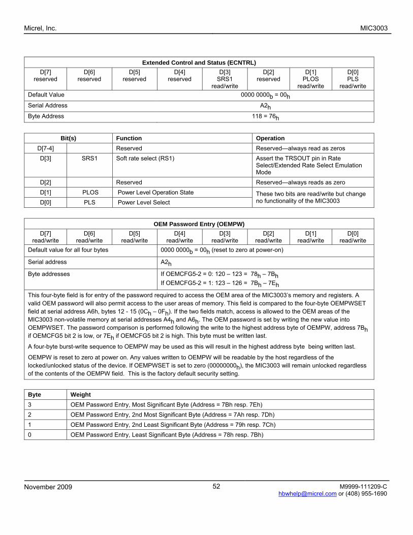
Micrel, Inc. MIC3003
November 2009 52 [email protected] or (408) 955-1690
Extended Control and Status (ECNTRL)
D[7] reserved
D[6] reserved
D[5] reserved
D[4] reserved
D[3] SRS1
read/write
D[2] reserved
D[1] PLOS
read/write
D[0] PLS
read/write Default Value 0000 0000b = 00h
Serial Address A2h
Byte Address 118 = 76h
Bit(s) Function Operation D[7-4] Reserved Reserved—always read as zeros D[3] SRS1 Soft rate select (RS1) Assert the TRSOUT pin in Rate
Select/Extended Rate Select Emulation Mode
D[2] Reserved Reserved—always reads as zero D[1] PLOS Power Level Operation State D[0] PLS Power Level Select
These two bits are read/write but change no functionality of the MIC3003
OEM Password Entry (OEMPW) D[7]
read/write D[6]
read/write D[5]
read/write D[4]
read/write D[3]
read/write D[2]
read/write D[1]
read/write D[0]
read/write Default value for all four bytes 0000 0000b = 00h (reset to zero at power-on)
Serial address A2h
Byte addresses If OEMCFG5-2 = 0: 120 – 123 = 78h – 7Bh If OEMCFG5-2 = 1: 123 – 126 = 7Bh – 7Eh
This four-byte field is for entry of the password required to access the OEM area of the MIC3003’s memory and registers. A valid OEM password will also permit access to the user areas of memory. This field is compared to the four-byte OEMPWSET field at serial address A6h, bytes 12 - 15 (0Ch – 0Fh). If the two fields match, access is allowed to the OEM areas of the MIC3003 non-volatile memory at serial addresses A4h and A6h. The OEM password is set by writing the new value into OEMPWSET. The password comparison is performed following the write to the highest address byte of OEMPW, address 7Bh if OEMCFG5 bit 2 is low, or 7Eh if OEMCFG5 bit 2 is high. This byte must be written last.
A four-byte burst-write sequence to OEMPW may be used as this will result in the highest address byte being written last.
OEMPW is reset to zero at power on. Any values written to OEMPW will be readable by the host regardless of the locked/unlocked status of the device. If OEMPWSET is set to zero (00000000h), the MIC3003 will remain unlocked regardless of the contents of the OEMPW field. This is the factory default security setting.
Byte Weight 3 OEM Password Entry, Most Significant Byte (Address = 7Bh resp. 7Eh) 2 OEM Password Entry, 2nd Most Significant Byte (Address = 7Ah resp. 7Dh) 1 OEM Password Entry, 2nd Least Significant Byte (Address = 79h resp. 7Ch) 0 OEM Password Entry, Least Significant Byte (Address = 78h resp. 7Bh)

Micrel, Inc. MIC3003
November 2009 53 [email protected] or (408) 955-1690
Power-On Hours (POHh and POHl) D[7]
read/write D[6]
read/write D[5]
read/write D[4]
read/write D[3]
read/write D[2]
read/write D[1]
read/write D[0]
read/write Default value of both bytes when the MIC3003 is shipped from the factory
0000 0000b = 00h
Serial address A6h
Bytes addresses MS byte (POHh): 251 = FBh LS byte (POHl): 252 = FCh
The lower seven bits of POHh contain the most significant bits of the 15-bit power-on hours measurement. The value in POHh should be combined with the eight-bit power-on hours low byte, POHl, to yield the complete result. The most significant bit of POHh, POHFLT, is an error flag. If POHFLT is set, the power-on hour meter data has been corrupted and should be ignored. It is recommended that a two-byte sequential (block) SMBus read operation be performed on POHh and POHl to insure coherency between the two registers. This register is non-volatile and will be maintained through power and reset cycles, including unanticipated power failures.
POHh Bit(s) Function Operation D[7] Power-on hours fault flag, POHFLT 1 = fault: the power-on hours value is corrupted and cannot
be relied upon 0 = no fault: the power-on hours value is correct
D[6:0] Power-on hours, most significant seven bits
Data Ready Flags (DATARDY) D[7]
TRDY read/write
D[6] VRDY
read/write
D[5] IRDY
read/write
D[4] TXRDY
read/write
D[3] RXDY
read/write
D[2] reserved
D[1] reserved
D[0] reserved
Default value 0000 0000b = 00h
Serial address A6h
Byte address 253 = FDh
When the A/D conversion for a given parameter is completed and the results available to the host, the appropriate data ready flag will be set. The flag will be cleared when the host reads the corresponding result register.
Bit(s) Function Operation D[7] TRDY Temperature data ready flag 0 = Result register contains old data; 1 = new data ready D[6] VRDY Voltage data ready flag 0 = Result register contains old data; 1 = new data ready D[5] IRDY Bias current data ready flag 0 = Result register contains old data; 1 = new data ready D[4] TXRDY Transmit power data ready flag 0 = Result register contains old data; 1 = new data ready D[3] RXRDY Receive power data ready flag 0 = Result register contains old data; 1 = new data ready
D[2:0] Reserved Reserved
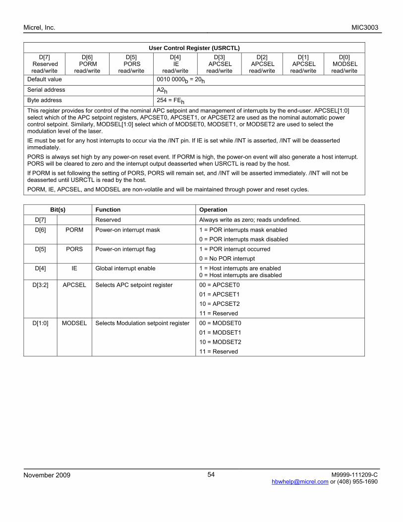
Micrel, Inc. MIC3003
November 2009 54 [email protected] or (408) 955-1690
User Control Register (USRCTL) D[7]
Reserved read/write
D[6] PORM
read/write
D[5] PORS
read/write
D[4] IE
read/write
D[3] APCSEL read/write
D[2] APCSEL read/write
D[1] APCSEL read/write
D[0] MODSEL read/write
Default value 0010 0000b = 20h
Serial address A2h
Byte address 254 = FEh
This register provides for control of the nominal APC setpoint and management of interrupts by the end-user. APCSEL[1:0] select which of the APC setpoint registers, APCSET0, APCSET1, or APCSET2 are used as the nominal automatic power control setpoint. Similarly, MODSEL[1:0] select which of MODSET0, MODSET1, or MODSET2 are used to select the modulation level of the laser. IE must be set for any host interrupts to occur via the /INT pin. If IE is set while /INT is asserted, /INT will be deasserted immediately. PORS is always set high by any power-on reset event. If PORM is high, the power-on event will also generate a host interrupt. PORS will be cleared to zero and the interrupt output deasserted when USRCTL is read by the host. If PORM is set following the setting of PORS, PORS will remain set, and /INT will be asserted immediately. /INT will not be deasserted until USRCTL is read by the host. PORM, IE, APCSEL, and MODSEL are non-volatile and will be maintained through power and reset cycles.
Bit(s) Function Operation D[7] Reserved Always write as zero; reads undefined.
D[6] PORM Power-on interrupt mask 1 = POR interrupts mask enabled 0 = POR interrupts mask disabled
D[5] PORS Power-on interrupt flag 1 = POR interrupt occurred 0 = No POR interrupt
D[4] IE Global interrupt enable 1 = Host interrupts are enabled 0 = Host interrupts are disabled
D[3:2] APCSEL Selects APC setpoint register 00 = APCSET0 01 = APCSET1 10 = APCSET2 11 = Reserved
D[1:0] MODSEL Selects Modulation setpoint register 00 = MODSET0 01 = MODSET1 10 = MODSET2 11 = Reserved
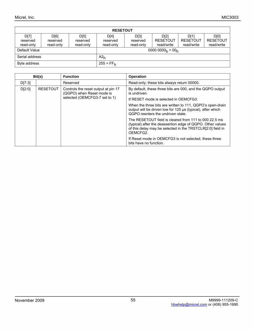
Micrel, Inc. MIC3003
November 2009 55 [email protected] or (408) 955-1690
RESETOUT D[7]
reserved read-only
D[6] reserved read-only
D[5] reserved read-only
D[4] reserved read-only
D[3] reserved read-only
D[2] RESETOUTread/write
D[1] RESETOUT read/write
D[0] RESETOUTread/write
Default Value 0000 0000b = 00h
Serial address A2h
Byte address 255 = FFh
Bit(s) Function Operation
D[7-3] Reserved Read-only; these bits always return 00000. D[2:0] RESETOUT Controls the reset output at pin 17
(QGPO) when Reset mode is selected (OEMCFG3-7 set to 1)
By default, these three bits are 000, and the QGPO output is undriven. If RESET mode is selected in OEMCFG3: When the three bits are written to 111, QGPO’s open-drain output will be driven low for 125 μs (typical), after which QGPO reenters the undriven state. The RESETOUT field is cleared from 111 to 000 22.5 ms (typical) after the deassertion edge of QGPO. Other values of this delay may be selected in the TRSTCLR[2:0] field in OEMCFG2. If Reset mode in OEMCFG3 is not selected, these three bits have no function.

Micrel, Inc. MIC3003
November 2009 56 [email protected] or (408) 955-1690
OEM Configuration Register 0 (OEMCFG0) D[7] RST
write only
D[6] QGPOS
read/write
D[5] DFLT
read-only
D[4] OE
reserved
D[3] MODREF reserved
D[2] VAUX[2] read/write
D[1] VAUX[1] read/write
D[0] VAUX[0] read/write
Default value 0000 0000b = 00h
Serial address A6h
Byte address 00 = 00h
A write to OEMCFG0 will result in any A/D conversion in progress being aborted and the result discarded. The A/D will begin a new conversion sequence once the write operation is complete. All bits in OEMCFG0 are non-volatile except DFLT and RST. A valid OEM password is required for access to this register.
Bit(s) Function Operation
D[7] RST 0 = no action; 1 = reset Issuing a software reset by setting RST high is equivalent to a full power cycle of the MIC3003.
D[6] QGPOS Determines the state of QGPO in GPO mode
If OEMCFG3 bit 7 (QGPOM) is low, this bit determines whether the QGPO output is high (undriven) or low (driven-open-drain). If QGPOM is high (Reset mode), this bit has no function
D[5] DFLT Diode fault flag. 1 = diode fault; 0 = OK. D[4] OE Output enable for SHDN, VMOD,
and VBIAS. 1 = enabled; 0 = hi-Z
D[3] MODREF Selects whether VMOD is referenced to ground or VDD.
1 = VDD; 0 = GND
D[2:0] VAUX[2:0] Selects the voltage reported in VINh:VINl.
000 = VIN
001 = VDDA
010 = VBIAS
011 = VMOD
100 = APCDAC 101 = MODDAC 110 = FLTDAC

Micrel, Inc. MIC3003
November 2009 57 [email protected] or (408) 955-1690
OEM Configuration Register 1 (OEMCFG1) D[7] INV
read/write
D[6] GAIN
read/write
D[5] BIASREF read/write
D[4] RFB[2]
read/write
D[3] RFB[1]
read/write
D[2] RFB[0]
read/write
D[1] SRCE
read/write
D[0] SPOL
read/write Default value 0000 0010b = 02h
Serial address A6h
Byte address 1 = 01h
A write to OEMCFG1 will result in any A/D conversion in progress being aborted and the result discarded. The A/D will begin a new conversion sequence once the write operation is complete. All bits in OEMCFG1 are non-volatile and will be maintained through power and reset cycles. A valid OEM password is required for access to this register.
Bit(s) Function Operation D[7] INV Inverts the APC op-amp inputs.
When low, the BIAS DAC output is connected to the “+”input and FB is connected to the “–” input of the op amp. Set low to use the APC feedback loop.
0 = emitter follower (no inversion); 1 = common emitter (inverted); read/write; non-volatile.
D[6] GAIN Sets the feedback voltage range by changing the APCDAC output swing; 0-VREF for optical feedback, 0-VREF/4 for electrical feedback.
1 = VREF/4 full scale; 0 = VREF full scale
D[5] BIASREF Selects whether FB and VMPD are referenced to ground or VDD and selects feedback resistor termination voltage (VDDA or GNDA).
1 = VDD; 0 = GNDA If this bit is set to 0, bit 1 should be set to 1 If this bit is set to 1, bit 1 should be set to 0
D[4:2] RFB[2:0] Selects internal feedback resistance. Resistors will be terminated to VDDA or GNDA according to BIASREF.
000 = ∞ 001 = 800 Ω 010 = 1.6kΩ 011 = 3.2kΩ 100 = 6.4kΩ 101 = 12.8kΩ 110 = 25.6kΩ 111 = 51.2kΩ
D[1] SRCE VBIAS source or sink drive. 1 = source (NPN): bit 5 should be set to 0. 0 = sink (PNP): bit 5 should be set to 1.
D[0] SPOL Polarity of the shutdown output, SHDN, when active.
1 = SHDN is active-high 0 = SHDN is active-low

Micrel, Inc. MIC3003
November 2009 58 [email protected] or (408) 955-1690
OEM Configuration Register 2 (OEMCFG2) D[7]
SMBADR[3] read/write
D[6] SMBADR[2] read/write
D[5] SMBADR[1] read/write
D[4] SMBADR[0] read/write
D[3]
read/write
D[2] TRSTCLR[2]
read/write
D[1] TRSTCLR[1]
read/write
D[0] TRSTCLR[0]
read/write Default value 1010 0010b = xxh (device address = 1010 xxxxb)
This value is the basis for using A0 h, A2 h, A4 h, and A6 h as the names of the different device address spaces of the MIC3003.
Serial address A6h
Byte address 2 = 02h
Caution: Changes to SMBADR take effect immediately. Any accesses following a write to SMBADR must be to the newly programmed serial bus address. A valid OEM password is required for access to this register. This register is non-volatile and will be maintained through power and reset cycles.
Bit(s) Function Operation D[7:4] SMBADR[3:0] Most significant four bits of the
serial bus device address Writes take effect immediately.
D[3:0] TRSTCLR[2:0] Set the delay between QGPO and the clearing of RESETOUT
These three bits set the delay between the deassertion edge of the QGPO output in Reset mode and the subsequent clearing of the three RESETOUT bits in the RESETOUT Register: 000: Zero delay 001: 17.5 ms typical 010: 22.5 ms typical (default) 011: 27.0 ms typical 100: 45 ms typical Minimum and maximum values may be found by adding tolerances of -10% and +10% to the above values. If Reset mode is not selected, these bits have no function.

Micrel, Inc. MIC3003
November 2009 59 [email protected] or (408) 955-1690
APC Setpoint 0, 1, and 2 (APCSET0, APCSET1, APCSET2) Automatic Power Control Setpoint
D[7] read/write
D[6] read/write
D[5] read/write
D[4] read/write
D[3] read/write
D[2] read/write
D[1] read/write
D[0] read/write
Default value for all three bytes 0000 0000b = 00h
Serial address A6h
Byte addresses APCSET0: 3 = 03h APCSET1: 4 = 04h APCSET2: 5 = 05h
When the APC is on, the eight-bit signed integer compensation value corresponding to the current temperature is taken from the BIASLUT look-up table, added to the selected APCSET (0, 1, or 2) register and loaded into the VBIAS DAC. If DAC Calibration mode is selected in OEMCAL0, a write to any one of the three APCSETn registers will cause the VBIAS DAC to be updated immediately. DAC Calibration mode disables the output of the BIASLUT lookup table, so the unmodified APCSETn register value propagates directly to the DAC. The eight-bit value presented to the VBIAS DAC is always available for readback in the APCDAC register. A valid OEM password is required for access to these registers. These registers are non-volatile and will be maintained through power and reset cycles.
Modulation Setpoint 0, 1, and 2 (MODSET0, MODSET1, and MODSET2) Nominal VMOD Setpoint
D[7] read/write
D[6] read/write
D[5] read/write
D[4] read/write
D[3] read/write
D[2] read/write
D[1] read/write
D[0] read/write
Default value for all three bytes 0000 0000b = 00h
Serial address A6h
Byte address MODSET0: 6 = 06h MODSET1: 30 = 1Eh MODSET2: 31 = 1Fh
When the APC is on, the eight-bit signed integer compensation value corresponding to the current temperature is taken from the MODLUT look-up table, added to the selected MODSET (0, 1, or 2) register and loaded into the VMOD DAC. If DAC Calibration mode is selected in OEMCAL0, a write to any one of the three MODSETn registers will cause the VMOD DAC to be updated immediately. DAC Calibration mode disables the output of the MODLUT lookup table, so the unmodified MODSETn register value propagates directly to the DAC. The eight-bit value presented to the VMOD DAC is always available for readback in the MODDAC register. A valid OEM password is required for access to these registers. These registers are non-volatile and will be maintained through power and reset cycles.
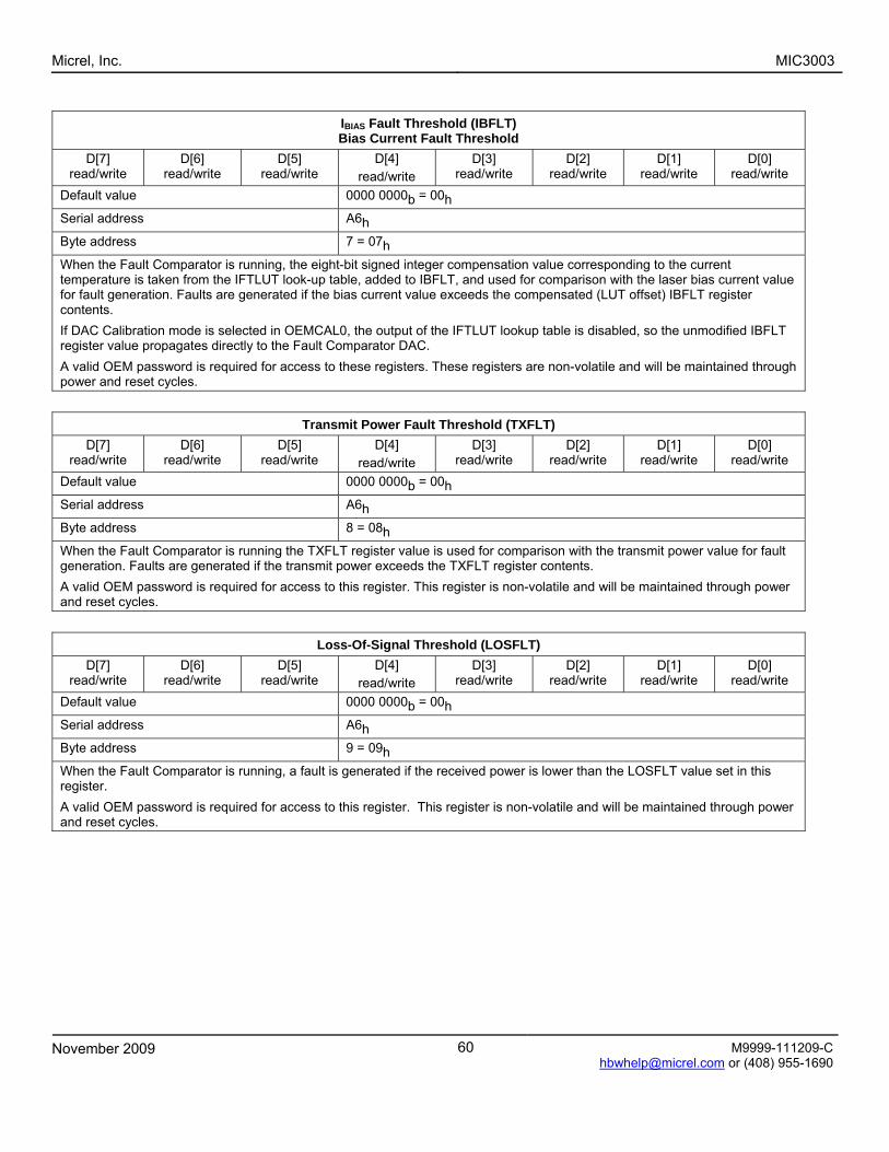
Micrel, Inc. MIC3003
November 2009 60 [email protected] or (408) 955-1690
IBIAS Fault Threshold (IBFLT) Bias Current Fault Threshold
D[7] read/write
D[6] read/write
D[5] read/write
D[4] read/write
D[3] read/write
D[2] read/write
D[1] read/write
D[0] read/write
Default value 0000 0000b = 00h
Serial address A6h
Byte address 7 = 07h
When the Fault Comparator is running, the eight-bit signed integer compensation value corresponding to the current temperature is taken from the IFTLUT look-up table, added to IBFLT, and used for comparison with the laser bias current value for fault generation. Faults are generated if the bias current value exceeds the compensated (LUT offset) IBFLT register contents. If DAC Calibration mode is selected in OEMCAL0, the output of the IFTLUT lookup table is disabled, so the unmodified IBFLT register value propagates directly to the Fault Comparator DAC. A valid OEM password is required for access to these registers. These registers are non-volatile and will be maintained through power and reset cycles.
Transmit Power Fault Threshold (TXFLT) D[7]
read/write D[6]
read/write D[5]
read/write D[4]
read/write D[3]
read/write D[2]
read/write D[1]
read/write D[0]
read/write Default value 0000 0000b = 00h
Serial address A6h
Byte address 8 = 08h
When the Fault Comparator is running the TXFLT register value is used for comparison with the transmit power value for fault generation. Faults are generated if the transmit power exceeds the TXFLT register contents. A valid OEM password is required for access to this register. This register is non-volatile and will be maintained through power and reset cycles.
Loss-Of-Signal Threshold (LOSFLT) D[7]
read/write D[6]
read/write D[5]
read/write D[4]
read/write D[3]
read/write D[2]
read/write D[1]
read/write D[0]
read/write Default value 0000 0000b = 00h
Serial address A6h
Byte address 9 = 09h
When the Fault Comparator is running, a fault is generated if the received power is lower than the LOSFLT value set in this register. A valid OEM password is required for access to this register. This register is non-volatile and will be maintained through power and reset cycles.
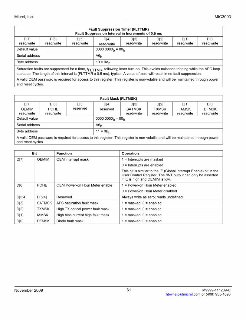
Micrel, Inc. MIC3003
November 2009 61 [email protected] or (408) 955-1690
Fault Suppression Timer (FLTTMR) Fault Suppression Interval in Increments of 0.5 ms
D[7] read/write
D[6] read/write
D[5] read/write
D[4] read/write
D[3] read/write
D[2] read/write
D[1] read/write
D[0] read/write
Default value 0000 0000b = 00h
Serial address A6h
Byte address 10 = 0Ah
Saturation faults are suppressed for a time, tFLTTMR, following laser turn-on. This avoids nuisance tripping while the APC loop starts up. The length of this interval is (FLTTMR x 0.5 ms), typical. A value of zero will result in no fault suppression. A valid OEM password is required for access to this register. This register is non-volatile and will be maintained through power and reset cycles.
Fault Mask (FLTMSK)
D[7] OEMIM
read/write
D[6] POHE
read/write
D[5] reserved
D[4] reserved
D[3] SATMSK read/write
D[2] TXMSK
read/write
D[1] IAMSK
read/write
D[0] DFMSK
read/write Default value 0000 0000b = 00h
Serial address A6h
Byte address 11 = 0Bh
A valid OEM password is required for access to this register. This register is non-volatile and will be maintained through power and reset cycles.
Bit Function Operation D[7] OEMIM OEM interrupt mask 1 = Interrupts are masked
0 = Interrupts are enabled This bit is similar to the IE (Global Interrupt Enable) bit in the User Control Register. The /INT output can only be asserted if IE is high and OEMIM is low.
D[6] POHE OEM Power-on Hour Meter enable 1 = Power-on Hour Meter enabled 0 = Power-on Hour Meter disabled
D[5:4] D[5:4] Reserved Always write as zero; reads undefined D[3] SATMSK APC saturation fault mask 1 = masked; 0 = enabled D[2] TXMSK High TX optical power fault mask 1 = masked; 0 = enabled D[1] IAMSK High bias current high fault mask 1 = masked; 0 = enabled D[0] DFMSK Diode fault mask 1 = masked; 0 = enabled

Micrel, Inc. MIC3003
November 2009 62 [email protected] or (408) 955-1690
OEM Password Setting (OEMPWSET) D[7]
read/write D[6]
read/write D[5]
read/write D[4]
read/write D[3]
read/write D[2]
read/write D[1]
read/write D[0]
read/write Default value for all bytes 0000 0000b = 00h
Serial address A6h
Byte addresses 12 - 15 = 0Ch - 0Fh
This four-byte field is the password required for access to the OEM area of the MIC3003’s memory and registers. This field is compared to the four-byte OEMPW field at serial address A2h. If the two fields match, access is allowed to the OEM areas of the MIC3003 non-volatile memory at serial addresses A4h and A6h. The OEM password may be set by writing the new value into OEMPWSET. The new password will not take effect until after a power-on reset occurs or a warm reset is performed using the RST bit in OEMCFG0. This allows the new password to be verified before it takes effect. These registers are non-volatile and will be maintained through power and reset cycles. A valid OEM password is required for access to this register.
Byte Weight 3 OEM Password, Most Significant Byte 2 OEM Password, 2nd Most Significant Byte 1 OEM Password, 2nd Least Significant Byte 0 OEM Password, Least Significant Byte
OEM Calibration 0 (OEMCAL0) D[7]
reserved read-only
D[6] FLTDIS
read/write
D[5] FSPIN
read/write
D[4] WRINH
read/write
D[3] APCCAL read/write
D[2] reserved read-only
D[1] reserved read-only
D[0] FRCOPS read/write
Default value 0000 0000b = 00h
Serial address A6h
Byte address 16 = 10h
A valid OEM password is required for access to this register. This register is volatile and will not keep its value through power cycles.

Micrel, Inc. MIC3003
November 2009 63 [email protected] or (408) 955-1690
Bit Function Operation D[7] Reserved Always write as zero; reads undefined. D[6] FLTDIS Fault Comparator disable 0 = Fault Comparator faults enabled
1 = Fault Comparator faults disabled When FLTDIS is high, the Fault Comparator does not run, and the following faults are not detected:
• High IBIAS faults • High transmit power faults • Low receive power faults
If a fault condition was detected prior to the assertion of FLTDIS, the fault flag will remain active until cleared, but cannot be set again until the Fault Comparator is allowed to run.
D[5] FSPIN Fault Comparator “spin-on-channel” mode select; do not enable ADC and FC spin-on-channel modes simultaneously.
0 = Normal Fault Comparator operation 1 = Force the Fault Comparator to spin on one channel When the Fault Comparator spins on just one channel (selected via OEMCAL1[1:0]), the two channels not being examined will not, of course, respond to fault conditions.
D[4] WRINH Inhibit NVRAM write cycles. 0 = Normal NVRAM operation 1 = Inhibit NVRAM writes When WRINH is high, writes to the MIC3003’s internal memory do not occur. Registers that are non-volatile are written with the new value, but will not retain that value through a power cycle, since the NVRAM backing storage has not been modified.
D[3] APCCAL Selects APC DAC calibration mode - DACs may be controlled directly.
0 = Normal mode 1 = DAC calibration mode. When DAC calibration mode is enabled, the temperature compensation lookup tables are disabled, so the DACs are presented with the values written into their corresponding registers.
D[2:1] Reserved Always write as zeros; reads undefined. D[0] FRCOPS Forces outputs for board-level or system-
level testing 0 = Normal operation 1 = Force outputs for testing: The following outputs are driven to their active states:
• TXFAULT (active polarity set in OEMCFG5) • /INT (only driven if the OEMIM bit is clear in
FLTMSK) • RXLOS (active polarity and RXLOS selection are
set in OEMCFG6)

Micrel, Inc. MIC3003
November 2009 64 [email protected] or (408) 955-1690
OEM Calibration 1 (OEMCAL1) D[7]
reserved read-only
D[6] ADSTP
read/write
D[5] ADIDL
read-only
D[4] ONESHOT read/write
D[3] ADSPIN
read/write
D[2] SPIN[2]
read/write
D[1] SPIN[1]
read/write
D[0] SPIN[0]
read/write
Default value 0000 0000b = 00h
Serial address A6h
Byte address 17 = 11h
A valid OEM password is required for access to this register. This register is volatile and will not keep its value through power cycles.
Bit Function Operation D[7] Reserved Always write as zero; reads undefined. D[6] ADSTP Stop ADC: Halts the analog to digital
converter 0 = ADC in normal operation 1 = ADC stopped When ADSTP is set, the five-channel ADC halts and no new ADC results are computed. Existing result registers are not changed. In addition, no new temperature compensation is applied to the APC loop and fault parameters, and no comparisons of the ADC results against the alarm and warning limits is performed.
D[5] ADIDL ADC idle flag 0 = ADC is busy 1 = ADC is idle ADIDL may be used in conjunction with ONESHOT to determine when the single ADC conversion is complete. After ONESHOT is set, the ADC runs until completion and then halts. Software may poll ADIDL to detect this completion before interrofating the result.
D[4] ONESHOT Triggers one-shot A/D conversion cycle 0 = Normal ADC operation 1 = ADC one-shot mode Setting ONESHOT high starts the ADC and causes it to stop after the next conversion is complete. After the conversion, the ADC remains stopped until ONESHOT is set low. Multiple single ADC conversions may be executed by repeatedly writing one to ONESHOT.
D[3] ADSPIN Selects ADC spin-on-channel mode; do not enable ADC and FC spin-on-channel modes simultaneously
0 = Normal ADC operation 1 = ADC spin-on-channel
D[2:0] SPIN[2:0] ADC and Fault Comparator (FC) channel select for spin-on-channel mode; do not enable ADC and FC spin-on-channel modes simultaneously
ADC: 000 = temperature 001 = voltage 010 = VILD 011 = VMPD 100 = VRX

Micrel, Inc. MIC3003
November 2009 65 [email protected] or (408) 955-1690
LUT Index (LUTINDX) D[7]
read-only D[6]
read-only D[5]
read-only D[4]
read-only D[3]
read-only D[2]
read-only D[1]
read-only D[0]
read-only Default value (before the first set of 16 temperature measurements has been accumulated)
0000 0000b = 00h
Serial address A6h
Byte address 18 = 12h The look-up table index is derived from the current temperature measurement as follows:
INDEX = TAVG / 2
where TAVG
is the current average temperature, averaged over a set of 16 samples. This register allows the current table index to be read by the host. The appropriate table base address must be added to LUTINDX to form a complete table index in physical memory. A valid OEM password is required for access to this register.
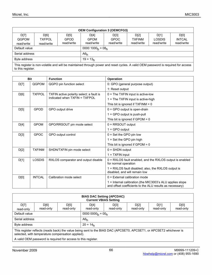
Micrel, Inc. MIC3003
November 2009 66 [email protected] or (408) 955-1690
OEM Configuration 3 (OEMCFG3) D[7]
QGPOM read/write
D[6] TXFPOL read/write
D[5] GPOD
read/write
D[4] GPOM
read/write
D[3] GPOC
read/write
D[2] TXFINM
read/write
D[1] LOSDIS
read/write
D[0] INTCAL
read/write Default value 0000 1000b = 08h
Serial address A6h
Byte address 19 = 13h
This register is non-volatile and will be maintained through power and reset cycles. A valid OEM password is required for access to this register.
Bit Function Operation
D[7] QGPOM QGPO pin function select 0: GPO (general purpose output) 1: Reset output
D[6] TXFPOL TXFIN active polarity select; a fault is indicated when TXFIN = TXFPOL
0 = The TXFIN input is active-low 1 = The TXFIN input is active-high This bit is ignored if TXFINM = 0
D[5] GPOD GPO output drive 0 = GPO output is open-drain 1 = GPO output is push-pull This bit is ignored if GPOM = 0
D[4] GPOM GPO/RRSOUT pin mode select 0 = RRSOUT output 1 = GPO output
D[3] GPOC GPO output control 0 = Set the GPO pin low 1 = Set the GPO pin high This bit is ignored if GPOM = 0
D[2] TXFINM SHDN/TXFIN pin mode select 0 = SHDN output 1 = TXFIN input
D[1] LOSDIS RXLOS comparator and output disable 0 = RXLOS fault enabled, and the RXLOS output is enabled for normal operation 1 = RXLOS fault disabled; also, the RXLOS output is disabled, and will remain low
D[0] INTCAL Calibration mode select 0 = External calibration mode 1 = Internal calibration.(the MIC3003’s ALU applies slope and offset coefficients to the ALU results as necessary)
BIAS DAC Setting (APCDAC) Current VBIAS Setting
D[7] read-only
D[6] read-only
D[5] read-only
D[4] read-only
D[3] read-only
D[2] read-only
D[1] read-only
D[0] read-only
Default value 0000 0000b = 00h
Serial address A6h
Byte address 20 = 14h
This register reflects (reads back) the value being sent to the BIAS DAC (APCSET0, APCSET1, or APCSET2 whichever is selected, with temperature compensation applied). A valid OEM password is required for access to this register.

Micrel, Inc. MIC3003
November 2009 67 [email protected] or (408) 955-1690
Modulation DAC Setting (MODDAC) Current VMOD Setting
D[7] read-only
D[6] read-only
D[5] read-only
D[4] read-only
D[3] read-only
D[2] read-only
D[1] read-only
D[0] read-only
Default value 0000 0000b = 00h
Serial address A6h
Byte address 21 = 15h
This register reflects (reads back) the value set in the being sent to the modulation DAC (MODSET0, MODSET1, or MODSET2 whichever is selected, with temperature compensation applied). A valid OEM password is required for access to this register.
OEM Readback Register (OEMRD) D[7]
Reserved read-only
D[6] KILL_LASER
read-only
D[5] RXP_FLT Read-only
D[4] INT
read-only
D[3] APCSAT read-only
D[2] IBFLT
read-only
D[1] TXFLT
read-only
D[0] RRSOUT read-only
Default value 0000 0000b = 00h
Serial address A6h
Byte address 22 = 16h
This register reflects (reads back) the status of the bits corresponding to the parameters defined below. A valid OEM password is required for access to this register.
Bit Function Operation D[7] Reserved Always reads as a zero D[6] KILL_LASER State of the internal laser disable
signal 0: The MIC3003 is disabling the laser 1: The laser is enabled to operate
D[5] RXP_FLT Registered Fault Comparator detection of a receive power fault
0: No Fault Comparator receive power fault 1: The Fault Comparator has detected a receive power fault
D[4] INT Mirrors state of /INT but active-high
1 = The interrupt is asserted 0 = No pending interrupt.
D[3] APCSAT Registered APC saturation fault 1 = APC saturation fault detected 0 = Normal operation.
D[2] IBFLT Registered Fault Comparator detection of an IBIAS fault
1 = IBIAS fault detected 0 = Normal operation
D[1] TXFLT Registered Fault Comparator detection of a transmit power fault
1 = Registered transmit power fault 0 = normal operation
D[0] TRSOUT State of the rate select output pin, TRSOUT
1 = high; 0 = low

Micrel, Inc. MIC3003
November 2009 68 [email protected] or (408) 955-1690
Signal Detect Threshold (LOSFLTn) D[7]
read/write D[6]
read/write D[5]
read/write D[4]
read/write D[3]
read/write D[2]
read/write D[1]
read/write D[0]
read/write Default value 0000 0000b = 00h
Serial address A6h
Byte address 23 = 17h
This eight-bit register works in conjunction with the LOSFLT register to provide hysteresis and control the operation of the loss of signal comparator. The comparator’s output, RXLOS, is asserted when the input on VRX falls below the level in LOSFLT. The output will then be deasserted when the VRX signal rises above the level in LOSFLTn. The input signal is subject to scaling by the RXPOT. If the LOS comparator is disabled, i.e., LOSDIS = 1, this register is ignored. A valid OEM password is required for access to this register. This register is non-volatile and will be maintained through power and reset cycles.
RX EEPOT Tap Selection (RXPOT) D[7]
reserved read-only
D[6] reserved read-only
D[5] reserved read-only
D[4] RXPOT[4] read/write
D[3] RXPOT[3] read/write
D[2] RXPOT[2] read/write
D[1] RXPOT[1] read/write
D[0] RXPOT[0] read/write
Default value 0000 0000b = 00h
Serial address A6h
Byte address 24 = 18h
This register is non-volatile and will be maintained through power and reset cycles. A valid OEM password is required for access to these registers.
Bit(s) Function Operation D[7:5] Reserved Reserved. Always write as zero; reads return zeros. D[4:0] RXPOT tap selection:
Adjust gain of the receive power measurement: 00000 = No divider action 00001 = 31/32 00010 = 30/32 • • • 11110 = 2/32 11111 = 1/32

Micrel, Inc. MIC3003
November 2009 69 [email protected] or (408) 955-1690
OEM Configuration 4 (OEMCFG4) D[7]
TXF_WRN read/write
D[6] TXF_ALM read/write
D[5] LAT_WRN read/write
D[4] LAT_ALM read/write
D[3] ISTART[3] read/write
D[2] ISTART[2] read/write
D[1] ISTART[1] read/write
D[0] ISTART[0] read/write
Default value 0000 0000b = 00h
Serial address A6h
Byte address 25 = 19h
This register is non-volatile and will be maintained through power and reset cycles. A valid OEM password is required for access to these registers.
Bit(s) Function Operation D[7] TXF_WRN Allows warnings to assert
TXFAULT
0: Warnings do not assert TXFAULT 1: Warnings assert TXFAULT The RXPWR low warning flag does not assert TXFAULT
D[6] TXF_ALM Allows alarms to assert TXFAULT
0: Alarms do not assert TXFAULT 1: Alarms assert TXFAULT The RXPWR low alarm flag does not assert TXFAULT
D[5] LAT_WRN Warning latch
0: Warnings flags are latched. They are cleared by reading the register or toggling TXDISABLE. 1: Warnings flags are not latched., i.e. they are set and reset with the warning condition. The flags are also cleared by reading the register or toggling TXDISABLE.
D[4] LAT_ALM Alarm latch
0: Alarms flags are latched. They are cleared by reading the register or toggling TXDISABLE. 1: Alarms flags are not latched., i.e. they are set and reset with alarm condition. The flags are also cleared by reading the register or toggling TXDISABLE.
D[3:0] ISTART[3:0] ISTART current level selection. ISTART current level selection:
0000 = No ISTART current 0001 - 1111 = 0.375 mA x ISTART[[3:0] ISTART is used to speed up the laser start-up after a fault occurs. The charging current of the compensation capacitor starts from ISTART instead of ramping up from 0.

Micrel, Inc. MIC3003
November 2009 70 [email protected] or (408) 955-1690
OEM Configuration 5 (OEMCFG5)
D[7] read/write
D[6] read/write
D[5] read/write
D[4] read/write
D[3] read/write
D[2] read/write
D[1] read/write
D[0] read/write
Default value 0000 0000b = 00h
Serial address A6h
Byte address 26 = 1Ah
This register is non-volatile and will be maintained through power and reset cycles. A valid OEM password is required for access to these registers.
Bit(s) Function Operation D[7] SHDN output enable / disable 0: SHDN is enabled. TXFAULT will trigger the SHDN output
1: SHDN is disabled. TXFAULT has no effect on the SHDN output This applies when pin 7 is set as the SHDN output
D[6] Lookup table temperature offset control
0: The temperature result used for the LUT access averaging algorithm does not have the offset coefficient applied 1: The temperature result used for the LUT access averaging algorithm is offset by the signed 6-bit (.5 C resolution) offset coefficient.
D[5] Temperature result register offset control
0: The temperature result register does not have the offset coefficient applied 1: The temperature result register is offset by the signed 6-bit (.5 C resolution) offset coefficient.
D[4] Polarity of TXFAULT
0: TXFAULT is active-high 1: TXFAULT is active-low
D[3] SMBus multipart support
0: Multipart mode off 1: Multipart mode on
D[2] OEM password location
0: A6h: 120-123 (78h-7Bh) 1: A6h: 123-126 (7Bh-7Eh)
D[1] SMBUS timeout enable / disable
0: SMBUS timeout enabled 1: SMBUS timeout disabled

Micrel, Inc. MIC3003
November 2009 71 [email protected] or (408) 955-1690
OEM Configuration 6 (OEMCFG6)
D[7] read/write
D[6] read/write
D[5] read/write
D[4] read/write
D[3] read/write
D[2] read/write
D[1] read/write
D[0] read/write
Default value 0000 0000b = 00h
Serial address A6h
Byte address 27 = 1Bh
This register is non-volatile and will be maintained through power and reset cycles. A valid OEM password is required for access to these registers.
Bit(s) Function Operation D[7] A0h space access control 0: A0h space is used according to SFF-8472
1: A0h space does not respond to any access request. SMBus transactions to A0h receive a NACK response.
D[6:5] RXPWR Linearization Intervals 00: Temperature-based coefficient selection 01: Programmable delimiters 10: Hard coded delimiters 11: Reserved Options 01 and 10 partition the receive power result range into eight regions, each of which has its own slope and offset coefficients. The delimiters identify the region boundaries within the 12-bit receive power range of results, and may be either hard-coded (10) or programmable (01). Use of hard-coded delimiters frees up exta A6 memory space for scratchpad use.
D[4] TXDISABLE debounce enable / disable
0: TXDISABLE is not debounced 1: TXDISABLE is debounced. Glitches less than 5 ms are rejected. Set this bit to 1 if a mechanical switch is used for TXDISABLE. Set to 0 for normal operation to assure compliance to the SFP MSA.
D[3] RXLOS Polarity
0: The RXLOS output is low for normal operation and high with a loss of signal condition. 1: The RXLOS output is high for normal operation (signal detected) and low with a loss of signal (no signal detected) condition.
D[2] RXLOS/TRSOUT Select 0: RXLOS is selected for output 1: TRRSOUT is selected for output
D[1] Temperature resolution
0: Temperature is measured to a resolution of 1 ºC (eight-bit resolution) 1: Temperature is measured to a resolution of 0.5 ºC (nine-bit resolution)
D[0] TXFAULT clear mode
0: TXFAULT remains set until TXDISABLE is toggled 1: TXFAULT is in continuous mode and follows the state of the faults In continuous mode, the fault conditions asserting TXFAULT are not registered and turn on and off According to the MIC3003’s operation.

Micrel, Inc. MIC3003
November 2009 72 [email protected] or (408) 955-1690
Power-On Hour Meter Data (POHDATA) D[7]
read/write D[6]
read/write D[5]
read/write D[4]
read/write D[3]
read/write D[2]
read/write D[1]
read/write D[0]
read/write Default values for all bytes when the MIC3003 is shipped
0000 0000b = 00h
Serial address A6h
Byte addresses 32 – 34 and 36 - 38 = 20h - 22h and 24h - 26h
These registers are used for backing up the POH result during power cycles. At power-up, the POH meter selects the larger of the two values as the initial count. Incremental results are stored in alternate register pairs. The power-on hour meter may be reset or preset by writing to these registers. These registers are not typically intended to be used by the OEM or end user. The current value of the power-on hours meter may be read from the POHh and POHl registers. If it is necessary to preset the power-on hours meter to a specific value, please consult the factory for the exact format to be written to the POHDATA registers. These registers are non-volatile and will be maintained through power and reset cycles. A valid OEM password is required for access to these registers.
Byte Weight 3 POHA, high-byte 2 POHA, low-byte 1 POHB, high-byte 0 POHB, low-byte
OEM Scratchpad Registers (SCRATCHn) Default value 0000 0000b = 00h
Serial address A6h
Byte addresses 136 - 207 (88 - CFh)
208 - 221 (D0 - DDh): This area is part of the OEM scratch pad only if the hard-coded delimiters option for receive power linearization is used.
222 - 250 (DE - FAh)
The scratchpad registers are general-purpose non-volatile memory locations. They can be freely read from and written to any time the MIC3003 is in OEM mode.

Micrel, Inc. MIC3003
November 2009 73 [email protected] or (408) 955-1690
RX Power Coefficient Look-up Table (RXLUTn) Default values Offset coefficients are set to a default value of zero
Slope coefficients are set to a default vakue of 1.0 Serial address A6h
Byte addresses 40 - 71 = 28h - 47h
These registers hold the receive power slope and offset coefficients used to calibrate the MIC3003’s ADC receive power result in internal calibration mode. These registers are non-volatile and will be maintained through power and reset cycles. A valid OEM password is required for access to these registers.
A6 Address Bytes Definition 40 (28h) RXSLP0h RX slope 0, high byte 41 (29h) RXSLP0l RX slope 0, low byte 42 (2Ah) RXOFF0h RX offset 0, high byte 43 (2Bh) RXOFF0l RX offset 0, low byte 44 (2Ch) RXSLP1h RX slope 1, high byte 45 (2Dh) RXSLP1l RX slope 1, low byte 46 (2Eh) RXOFF1h RX offset 1, high byte 47 (2Fh) RXOFF1l RX offset 1, low byte
• • • • • •
68 (44h) RXSLP7h RX slope 7, high byte 69 (45h) RXSLP7l RX slope 7, low byte 70 (46h) RXOFF7h RX offset 7, high byte 71 (47h) RXOFF7l RX offset 7, low byte
Calibration Constants (CALCOEFn) Default values Offset coefficients are set to a default value of zero
Slope coefficients are set to a default vakue of 1.0 Serial address A6h
Byte addresses 74 - 87 = 4Ah - 57h These registers hold the slope and offset coefficients used to calibrate the MIC3003’s ADC results in internal calibration mode. Note that the temperature offset is also used in external calibration mode; but this can be disabled in OEMCFG5 (or by setting the offset coefficient to zero). These registers are non-volatile and will be maintained through power and reset cycles. A valid OEM password is required for access to these registers.
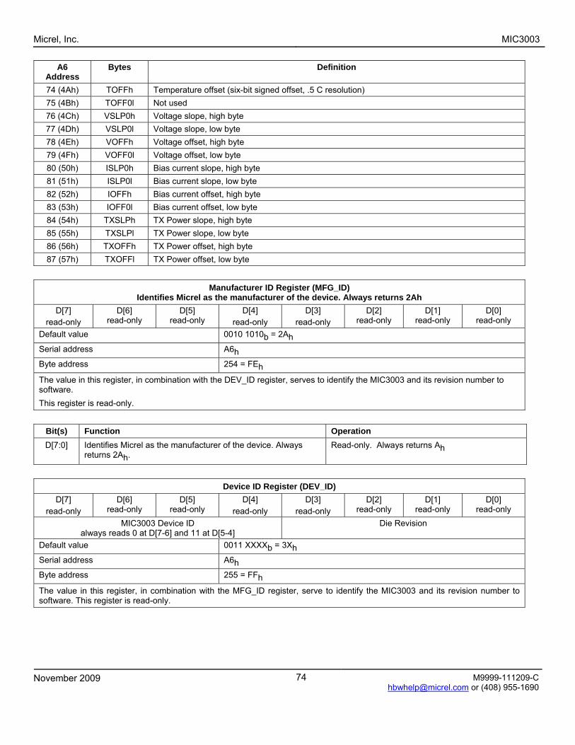
Micrel, Inc. MIC3003
November 2009 74 [email protected] or (408) 955-1690
A6 Address
Bytes Definition
74 (4Ah) TOFFh Temperature offset (six-bit signed offset, .5 C resolution) 75 (4Bh) TOFF0l Not used 76 (4Ch) VSLP0h Voltage slope, high byte 77 (4Dh) VSLP0l Voltage slope, low byte 78 (4Eh) VOFFh Voltage offset, high byte 79 (4Fh) VOFF0l Voltage offset, low byte 80 (50h) ISLP0h Bias current slope, high byte 81 (51h) ISLP0l Bias current slope, low byte 82 (52h) IOFFh Bias current offset, high byte 83 (53h) IOFF0l Bias current offset, low byte 84 (54h) TXSLPh TX Power slope, high byte 85 (55h) TXSLPl TX Power slope, low byte 86 (56h) TXOFFh TX Power offset, high byte 87 (57h) TXOFFl TX Power offset, low byte
Manufacturer ID Register (MFG_ID) Identifies Micrel as the manufacturer of the device. Always returns 2Ah
D[7] read-only
D[6] read-only
D[5] read-only
D[4] read-only
D[3] read-only
D[2] read-only
D[1] read-only
D[0] read-only
Default value 0010 1010b = 2Ah
Serial address A6h
Byte address 254 = FEh
The value in this register, in combination with the DEV_ID register, serves to identify the MIC3003 and its revision number to software. This register is read-only.
Bit(s) Function Operation D[7:0] Identifies Micrel as the manufacturer of the device. Always
returns 2Ah. Read-only. Always returns Ah
Device ID Register (DEV_ID) D[7]
read-only D[6]
read-only D[5]
read-only D[4]
read-only D[3]
read-only D[2]
read-only D[1]
read-only D[0]
read-only MIC3003 Device ID
always reads 0 at D[7-6] and 11 at D[5-4] Die Revision
Default value 0011 XXXXb = 3Xh
Serial address A6h
Byte address 255 = FFh
The value in this register, in combination with the MFG_ID register, serve to identify the MIC3003 and its revision number to software. This register is read-only.

Micrel, Inc. MIC3003
November 2009 75 [email protected] or (408) 955-1690
Package Information
24-Pin MLF® (MLF-24)
MICREL, INC. 2180 FORTUNE DRIVE SAN JOSE, CA 95131 USA TEL +1 (408) 944-0800 FAX +1 (408) 474-1000 WEB http:/www.micrel.com
The information furnished by Micrel in this data sheet is believed to be accurate and reliable. However, no responsibility is assumed by Micrel for its
use. Micrel reserves the right to change circuitry and specifications at any time without notification to the customer.
Micrel Products are not designed or authorized for use as components in life support appliances, devices or systems where malfunction of a product can reasonably be expected to result in personal injury. Life support devices or systems are devices or systems that (a) are intended for surgical
implant into the body or (b) support or sustain life, and whose failure to perform can be reasonably expected to result in a significant injury to the user. A Purchaser’s use or sale of Micrel Products for use in life support appliances, devices or systems is a Purchaser’s own risk and Purchaser agrees to
fully indemnify Micrel for any damages resulting from such use or sale.
© 2009 Micrel, Incorporated.