mh248 high sensitivity micropower hall effect switch...
TRANSCRIPT

010612 Page 1 of 14 Rev. 1.12
MH248 High Sensitivity Micropower Hall Effect Switch
MH248 Hall-effect sensor is a temperature stable, stress-resistant , micro-power switch. Superior high-temperature performance is made possible through a dynamic offset cancellation that utilizes chopper-stabilization. This method reduces the offset voltage normally caused by device over molding, temperature dependencies, and thermal stress.
MH248 includes the following on a single silicon chip: voltage regulator, Hall voltage
generator, small-signal amplifier, chopper stabilization, Schmitt trigger, open-drain output. Advanced CMOS wafer fabrication processing is used to take advantage of low-voltage requirements, component matching, very low input-offset errors, and small component geometries.
This device requires the presence of omni-polar magnetic fields for operation.
MH248 is rated for operation between the ambient temperatures –40℃ and + 85℃ for the E temperature range. The four package styles available provide magnetically optimized solutions for most applications. Package types SO is an SOT-23(1.1 mm nominal height),SQ is an QFN2020-3(0.5 mm nominal height),Tsot-23 is an ST(0.7 mm nominal height) ,a miniature low-profile surface-mount package, while package UA is a three-lead ultra-mini SIP for through-hole mounting.
The package type is in a lead (Pb)-free/ Green version was verified by third party Lab.
Features and Benefits CMOS Hall IC Technology Solid-State Reliability Micro power consumption for battery-powered applications Omni polar, output switches with absolute value of North or South pole from magnet Operation down to 2.5 V and Max at 3.5V. High Sensitivity for direct reed switch replacement applications Multi Small Size option Custom sensitivity selection is available in optional package. Pb Free/Green chip is qualified by third party lab.
Applications Solid state switch Handheld Wireless Handset Awake Switch ( Flip Cell/PHS Phone/Note Book/Flip
Video Set) Lid close sensor for battery powered devices Magnet proximity sensor for reed switch replacement in low duty cycle applications

010612 Page 2 of 14 Rev. 1.12
MH248 High Sensitivity Micropower Hall Effect Switch
Ordering Information
Part No. Temperature Suffix Package Type MH248EUA E (-40℃ to + 85℃) UA (TO-92S)
MH248ESO E (-40℃ to + 85℃) SO (SOT-23)
MH248EST E (-40℃ to + 85℃) ST (TSOT-23)
MH248ESQ E (-40℃ to + 85℃) SQ (QFN2020-3)
MH248ESO-α E (-40℃ to + 85℃) SO (SOT-23)
MH248ESO-β E (-40℃ to + 85℃) SO (SOT-23)
MH248ESO-γ E (-40℃ to + 85℃) SO (SOT-23)
Custom sensitivity selection is available by MST sorting technology Functional Diagram
Awake/SleepTiming Control
Amp Control Logic
Offset Cancellation
VDD
Out
GND
Hall Sensor
Note: Static sensitive device; please observe ESD precautions. Reverse VDD protection is not included. For reverse voltage protection, a 100Ω resistor in series with VDD is recommended.
XXXXXXXXX - X
Company Name and Product Category
Temperature Code
Part number
Sorting Code
Package type
Company Name and Product Category
MH:MST Hall Effect/MP:MST Power MOSFET
Part number
181,182,183,184,185,248,249,276,477,381,381F,381R,382…..
If part # is just 3 digits, the forth digit will be omitted.
Temperature range
E: 85 ℃, I: 105 ℃, K: 125 ℃, L: 150 ℃
Package type
UA:TO-92S,VK:TO-92S(4pin),VF:TO-92S(5pin),SO:SOT-23,
SQ:QFN-3,ST:TSOT-23,SN:SOT-553,SF:SOT-89(5pin)
Sorting
α,β,Blank…..
010612 Page 3 of 14 Rev. 1.12
MH248 High Sensitivity Micropower Hall Effect Switch
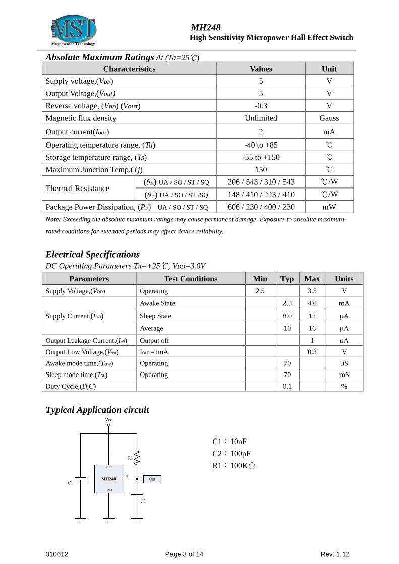
C1:10nF C2:100pF R1:100KΩ
Absolute Maximum Ratings At (Ta=25℃) Characteristics Values Unit
Supply voltage,(VDD) 5 V Output Voltage,(Vout) 5 V Reverse voltage, (VDD) (VOUT) -0.3 V Magnetic flux density Unlimited Gauss
Output current(IOUT) 2 mA
Operating temperature range, (Ta) -40 to +85 ℃ Storage temperature range, (Ts) -55 to +150 ℃ Maximum Junction Temp,(Tj) 150 ℃
Thermal Resistance (θJA) UA / SO / ST / SQ 206 / 543 / 310 / 543 ℃/W (θJC) UA / SO / ST /SQ 148 / 410 / 223 / 410 ℃/W
Package Power Dissipation, (PD) UA / SO / ST / SQ 606 / 230 / 400 / 230 mW Note: Exceeding the absolute maximum ratings may cause permanent damage. Exposure to absolute maximum-
rated conditions for extended periods may affect device reliability.
Electrical Specifications DC Operating Parameters TA=+25℃, VDD=3.0V
Parameters Test Conditions Min Typ Max Units Supply Voltage,(VDD) Operating 2.5 3.5 V
Supply Current,(IDD)
Awake State 2.5 4.0 mA
Sleep State 8.0 12 μA
Average 10 16 μA
Output Leakage Current,(Ioff) Output off 1 uA Output Low Voltage,(Vsat) IOUT=1mA 0.3 V Awake mode time,(Taw)
Operating 70 uS Sleep mode time,(TSL)
Operating 70 mS Duty Cycle,(D,C) 0.1 %
Typical Application circuit
OutC1
MH182MH248
Vcc
R1
C2
VDD
Out
GND

010612 Page 4 of 14 Rev. 1.12
MH248 High Sensitivity Micropower Hall Effect Switch
MH248E UA/SQ Magnetic Specifications DC Operating Parameters TA=+25℃, VDD=3.0V Parameter Symbol Test Conditions Min. Typ. Max. Units Operating
Point
BOPS S pole to branded side, B > BOP, Vout On 6 60 Gauss
BOPN N pole to branded side, B > BOP, Vout On -60 -6 Gauss
Release
Point
BRPS S pole to branded side, B < BRP, Vout Off 5 59 Gauss
BRPN N pole to branded side, B < BRP, Vout Off -60 -5 Gauss
Hysteresis BHYS |BOPx - BRPx| 7 Gauss
MH248E SO/ST Magnetic Specifications DC Operating Parameters TA=+25℃, VDD=3.0V
Parameter Symbol Test Conditions Min. Typ. Max. Units Operating
Point
BOPS N pole to branded side, B > BOP, Vout On 6 60 Gauss
BOPN S pole to branded side, B > BOP, Vout On -60 -6 Gauss
Release
Point
BRPS N pole to branded side, B < BRP, Vout Off 5 59 Gauss
BRPN S pole to branded side, B < BRP, Vout Off -60 -5 Gauss
Hysteresis BHYS |BOPx - BRPx| 7 Gauss
MH248ESO-α Magnetic Specifications DC Operating Parameters TA=+25℃, VDD=3.0V
Parameter Symbol Test Conditions Min. Typ. Max. Units Operating
Point
BOPS N pole to branded side, B > BOP, Vout On 21 40 Gauss
BOPN S pole to branded side, B > BOP, Vout On -60 -6 Gauss
Release
Point
BRPS N pole to branded side, B < BRP, Vout Off 39 Gauss
BRPN S pole to branded side, B < BRP, Vout Off -59 Gauss
Hysteresis BHYS |BOPx - BRPx| 7 Gauss
MH248ESO-β Magnetic Specifications DC Operating Parameters TA=+25℃, VDD=3.0V
Parameter Symbol Test Conditions Min. Typ. Max. Units Operating
Point
BOPS N pole to branded side, B > BOP, Vout On 31 60 Gauss
BOPN S pole to branded side, B > BOP, Vout On -60 -6 Gauss
Release
Point
BRPS N pole to branded side, B < BRP, Vout Off 59 Gauss
BRPN S pole to branded side, B < BRP, Vout Off -59 Gauss
Hysteresis BHYS |BOPx - BRPx| 7 Gauss
010612 Page 5 of 14 Rev. 1.12
MH248 High Sensitivity Micropower Hall Effect Switch
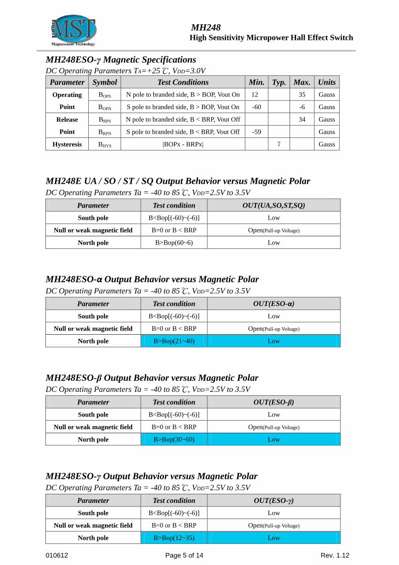
MH248ESO-γ Magnetic Specifications DC Operating Parameters TA=+25℃, VDD=3.0V
Parameter Symbol Test Conditions Min. Typ. Max. Units Operating
Point
BOPS N pole to branded side, B > BOP, Vout On 12 35 Gauss
BOPN S pole to branded side, B > BOP, Vout On -60 -6 Gauss
Release
Point
BRPS N pole to branded side, B < BRP, Vout Off 34 Gauss
BRPN S pole to branded side, B < BRP, Vout Off -59 Gauss
Hysteresis BHYS |BOPx - BRPx| 7 Gauss
MH248E UA / SO / ST / SQ Output Behavior versus Magnetic Polar DC Operating Parameters Ta = -40 to 85℃, VDD=2.5V to 3.5V
Parameter Test condition OUT(UA,SO,ST,SQ)
South pole B<Bop[(-60)~(-6)] Low
Null or weak magnetic field B=0 or B < BRP Open(Pull-up Voltage)
North pole B>Bop(60~6) Low
MH248ESO-α Output Behavior versus Magnetic Polar DC Operating Parameters Ta = -40 to 85℃, VDD=2.5V to 3.5V
Parameter Test condition OUT(ESO-α)
South pole B<Bop[(-60)~(-6)] Low
Null or weak magnetic field B=0 or B < BRP Open(Pull-up Voltage)
North pole B>Bop(21~40) Low
MH248ESO-β Output Behavior versus Magnetic Polar DC Operating Parameters Ta = -40 to 85℃, VDD=2.5V to 3.5V
Parameter Test condition OUT(ESO-β)
South pole B<Bop[(-60)~(-6)] Low
Null or weak magnetic field B=0 or B < BRP Open(Pull-up Voltage)
North pole B>Bop(30~60) Low
MH248ESO-γ Output Behavior versus Magnetic Polar DC Operating Parameters Ta = -40 to 85℃, VDD=2.5V to 3.5V
Parameter Test condition OUT(ESO-γ)
South pole B<Bop[(-60)~(-6)] Low
Null or weak magnetic field B=0 or B < BRP Open(Pull-up Voltage)
North pole B>Bop(12~35) Low

010612 Page 6 of 14 Rev. 1.12
MH248 High Sensitivity Micropower Hall Effect Switch
SO/ST package UA package SQ package
VsatBOPN BRPN BRPS BOPS
High State
Low State Low State
Out
put
Vol
tage
in
Vol
ts
Magnetic Flux Density in Gauss
0
High State
Performance Graph
Typical Supply Voltage(VDD) Versus Flux Density
Typical Temperature(TA) Versus Flux Density
Typical Temperature(TA) Versus Supply Current(IDD)
Typical Supply Voltage(VDD) Versus Supply Current(IDD)
-50.0
-40.0
-30.0
-20.0
-10.0
0.0
10.0
20.0
30.0
40.0
50.0
2.5 2.6 2.7 2.8 2.9 3.0 3.3 3.5
Flu
x D
ensi
ty(G
auss
)
Supply Voltage(V)
BOPSBOPNBRPSBRPN
-50.0
-40.0
-30.0
-20.0
-10.0
0.0
10.0
20.0
30.0
40.0
50.0
-40 -20 0 20 40 55 70 85
Flu
x D
ensi
ty(G
auss
)
Temperature(℃)
BOPSBOPNBRPSBRPN
0.00
2.00
4.00
6.00
8.00
10.00
12.00
14.00
16.00
18.00
20.00
-40 -20 0 20 40 55 70 85
Cur
rent
Con
sum
ptio
n
Temperature(℃)
Sleep Current(uA)Awarke Current(mA)Average Current(uA)
0.00
2.00
4.00
6.00
8.00
10.00
12.00
14.00
16.00
18.00
20.00
2.5 2.6 2.7 2.8 2.9 3.0 3.3 3.5
Cur
rent
Con
sum
ptio
n
Supply Voltage(V)
Sleep Current(uA)Awarke Current(mA)Average Current(uA)
North PoleSouth Pole
North Pole South Pole
North Pole South Pole

010612 Page 7 of 14 Rev. 1.12
MH248 High Sensitivity Micropower Hall Effect Switch
Typical Supply Voltage(VDD) Versus Output Voltage(VDSON)
Typical Temperature(TA) Versus Output Voltage(VDSON)
Typical Supply Voltage(VDD) Versus Leakage Current(IOFF)
Power Dissipation versus Temperature(TA)
Package Power Dissipation The power dissipation of the Package is a function of the pad size. This can vary from the minimum pad size for soldering to a pad size given for maximum power dissipation. Power dissipation for a surface mount device is determined by TJ(max), the maximum rated junction temperature of the die, RθJA, the thermal resistance from the device junction to ambient, and the operating temperature, Ta. Using the values provided on the data sheet for the package, PD can be calculated as follows:
a j
J(max)D R
Ta-TP
θ
=
The values for the equation are found in the maximum ratings table on the data sheet. Substituting these values into the equation for an ambient temperature Ta of 25°C, one can calculate the power dissipation of the device which in this case is 606 milliwatts.
0.0
5.0
10.0
15.0
20.0
25.0
30.0
35.0
40.0
45.0
50.0
2.5 2.6 2.7 2.8 2.9 3.0 3.3 3.5
Out
put S
atur
atio
n V
olta
ge (m
V)
Supply Voltage(V)
0.0
5.0
10.0
15.0
20.0
25.0
30.0
35.0
40.0
45.0
50.0
-40 -20 0 20 40 55 70 85
Out
put S
atur
atio
n V
olta
ge (m
V)
Temperature(℃)
0.000
0.010
0.020
0.030
0.040
0.050
2.5 2.6 2.7 2.8 2.9 3.0 3.3 3.5
Out
put L
eaka
ge C
urre
nt(u
A)
Supply Voltage(V)
0
100
200
300
400
500
600
700
-40 0 40 80 120 160
Pack
age
pow
er D
issi
patio
n(m
W)
Temperature(℃)
UA Package
Rθja = 206℃/w
ST Package
Rθja = 310℃/w
SO/SQ Package
Rθja = 543℃/w
010612 Page 8 of 14 Rev. 1.12
MH248 High Sensitivity Micropower Hall Effect Switch
606mWC/206
C25-C150(UA)PW
D =°
°°=
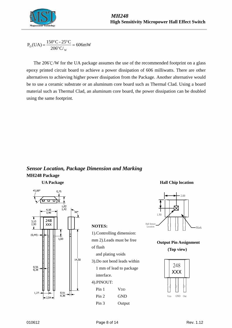
The 206℃/W for the UA package assumes the use of the recommended footprint on a glass epoxy printed circuit board to achieve a power dissipation of 606 milliwatts. There are other alternatives to achieving higher power dissipation from the Package. Another alternative would be to use a ceramic substrate or an aluminum core board such as Thermal Clad. Using a board material such as Thermal Clad, an aluminum core board, the power dissipation can be doubled using the same footprint. Sensor Location, Package Dimension and Marking MH248 Package
UA Package Hall Chip location
248XXX
NOTES: 1).Controlling dimension: mm 2).Leads must be free of flash and plating voids 3).Do not bend leads within
1 mm of lead to package interface.
4).PINOUT: Pin 1 VDD Pin 2 GND Pin 3 Output
Output Pin Assignment (Top view)
1 2 3
VDD GND Out
248
XXX
1.50
2.00
Hall SensorLocation Mark

010612 Page 9 of 14 Rev. 1.12
MH248 High Sensitivity Micropower Hall Effect Switch
SO Package Hall Plate Chip Location (Top View) (Bottom view)
248XX1 2
3
ST Package (TSOT-23) Hall Plate Chip Location (Top View) (Bottom view)
NOTES:
1. PINOUT (See Top View at left :) Pin 1 VDD Pin 2 Output Pin 3 GND
2. Controlling dimension: mm 3. Lead thickness after solder plating
will be 0.254mm maximum
0.80
1.45Hall Sensor
Location
12
3
248XX1 2
3
0.80
1.45Hall Sensor
Location
12
3
NOTES:
1. PINOUT (See Top View at left:)
Pin 1 VDD
Pin 2 Output
Pin 3 GND
2. Controlling dimension: mm;

010612 Page 10 of 14 Rev. 1.12
MH248 High Sensitivity Micropower Hall Effect Switch
SQ Package
248XX
1 2
3
MH248 UA(TO-92S) Package Date Code
X X X
Year Week
EX:2012 Year_8 Week → 208 MH248 SO(SOT-23)/ ST(TSOT-23)/ SQ(QFN2020-3) Package Date Code
X X
Week Code
1
Hall SensorLocation 1 2
1
3
Hall Plate Chip Location
(Top view)
NOTES:
3. PINOUT (See Top View
at left)
Pin 1 VDD
Pin 2 Output
Pin 3 GND
4. Controlling dimension:
mm;
5. Chip rubbing will be
10mil maximum;
6. Chip must be in PKG.
center.
010612 Page 11 of 14 Rev. 1.12
MH248 High Sensitivity Micropower Hall Effect Switch
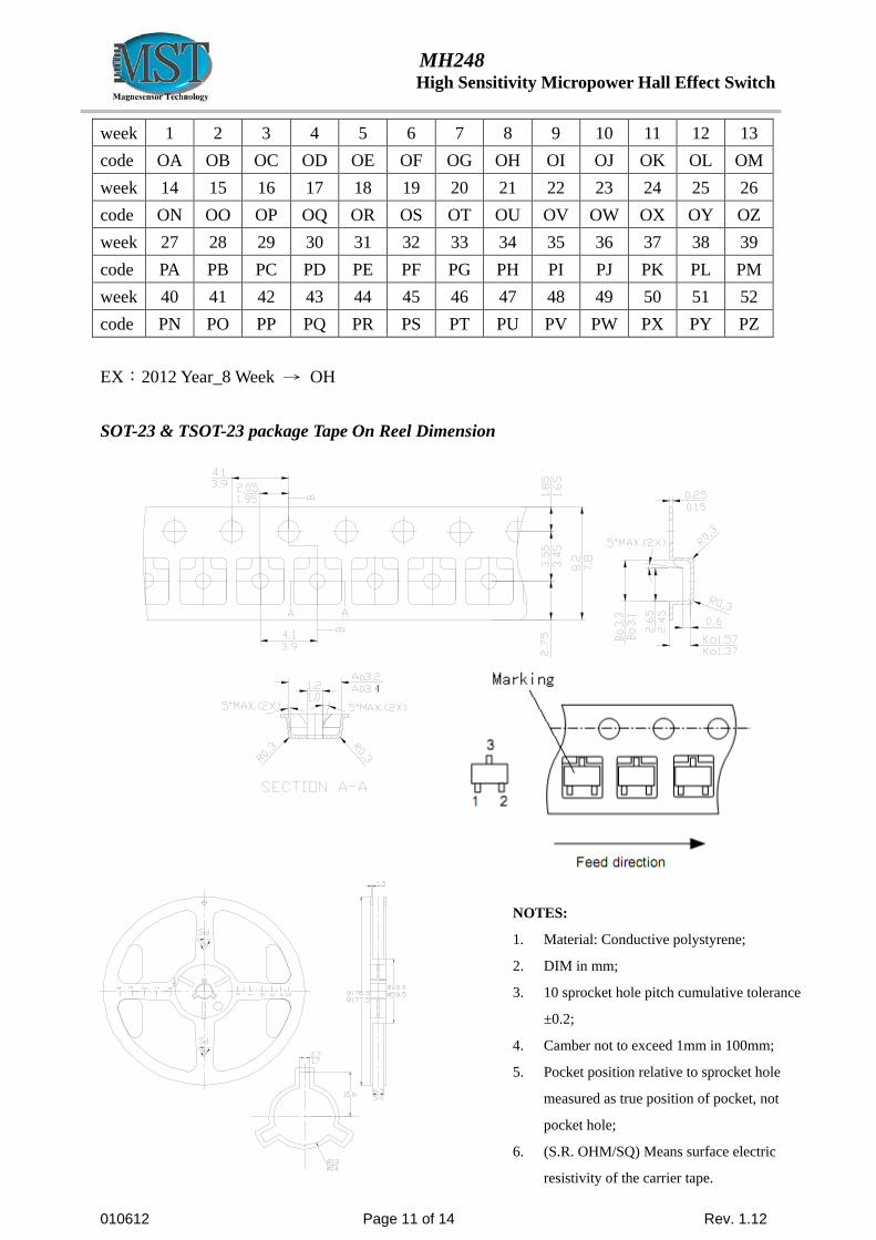
week 1 2 3 4 5 6 7 8 9 10 11 12 13 code OA OB OC OD OE OF OG OH OI OJ OK OL OM week 14 15 16 17 18 19 20 21 22 23 24 25 26 code ON OO OP OQ OR OS OT OU OV OW OX OY OZ week 27 28 29 30 31 32 33 34 35 36 37 38 39 code PA PB PC PD PE PF PG PH PI PJ PK PL PM week 40 41 42 43 44 45 46 47 48 49 50 51 52 code PN PO PP PQ PR PS PT PU PV PW PX PY PZ EX:2012 Year_8 Week → OH SOT-23 & TSOT-23 package Tape On Reel Dimension
4
NOTES:
1. Material: Conductive polystyrene;
2. DIM in mm;
3. 10 sprocket hole pitch cumulative tolerance
±0.2;
4. Camber not to exceed 1mm in 100mm;
5. Pocket position relative to sprocket hole
measured as true position of pocket, not
pocket hole;
6. (S.R. OHM/SQ) Means surface electric
resistivity of the carrier tape.
010612 Page 12 of 14 Rev. 1.12
MH248 High Sensitivity Micropower Hall Effect Switch
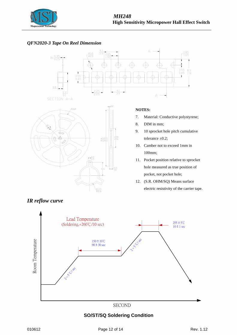
QFN2020-3 Tape On Reel Dimension
IR reflow curve
2 ~
5 ℃
/ sec
2 ~
5 ℃
/ sec150 ± 10℃
90 ± 30 sec
255 ± 5℃10 ± 1 sec
Roo
m T
empe
ratu
re
SECOND
Lead Temperature (Soldering,+260℃/10 sec)
SO/ST/SQ Soldering Condition
NOTES:
7. Material: Conductive polystyrene;
8. DIM in mm;
9. 10 sprocket hole pitch cumulative
tolerance ±0.2;
10. Camber not to exceed 1mm in
100mm;
11. Pocket position relative to sprocket
hole measured as true position of
pocket, not pocket hole;
12. (S.R. OHM/SQ) Means surface
electric resistivity of the carrier tape.

010612 Page 13 of 14 Rev. 1.12
MH248 High Sensitivity Micropower Hall Effect Switch
2 ~
5 ℃
/ sec
2 ~
5 ℃
/ sec
150 ± 10℃90 ± 30 sec
240 ± 5℃10 ± 1 sec
Roo
m T
empe
ratu
re
SECOND
Lead Temperature (Soldering,+245℃/10 sec)
UA Soldering Condition
Packing specification:
Package Bag Box Carton
TO-92S-3L 1,000pcs/bag 10bag/box 8 box/carton
SOT-23-3L 3,000pcs/reel 10 reel/box box/carton
TSOT-23-3L 3,000pcs/reel 10 reel/box box/carton
QFN2020-3 3,000pcs/reel 10 reel/box box/carton
TO-92S-3L Weight SOT-23-3L
TSOT-23-3L Weight QFN2020-3 Weight
1000pcs/bag 0.11kg 3000pcs/reel 0.18kg 3000pcs/reel 0.13kg
10 bags/box 1.24kg 10 reels/box 1.99kg 10 reels/box 1.40kg
8 boxes/carton 10.09kg 2 boxes/carton 4.9kg 2boxes/carton 3.70kg

010612 Page 14 of 14 Rev. 1.12
MH248 High Sensitivity Micropower Hall Effect Switch
Inner box label: Bag and inner box PB free Label Bag and inner box Green Label
Size: 3.4cm*6.4cm
Carton label:
Size: 5.6 cm * 9.8 cm
Combine: When combine lot, one reel could have two D/C and no more than two DC. One carton could have two devices, no more than two;