mgj6 full bridge series · mgj6 full bridge series 5.7kvdc isolated 6w triple output gate drive sm...
TRANSCRIPT

MGJ6 Full Bridge Series5.7kVDC Isolated 6W Triple Output Gate Drive SM DC-DC Converters
KDC_MGJ6C-FB.B02 Page 1 of 14
www.murata-ps.com
www.murata-ps.com/support
For full details go towww.murata-ps.com/rohs
FEATURES
No opto feedback
Patent protected
Three isolated output voltages suitable for IGBT/SiC & Mosfet gate drives in a full bridge configuration
Reinforced insulation to UL60950 with 8mm creepage & clearance recognition pending
ANSI/AAMI ES60601-1 recognition pending
Characterised dv/dt immunity 80kV/μs at 1.6kV
Characterised partial discharge performance
5.7kVDC isolation test voltage ‘Hi Pot Test’
Ultra low coupling capacitance typically 15pF
DC link voltage 3kVDC
5V, 12V & 24V input voltages
105°C operating temperature
PRODUCT OVERVIEW
Offering Three isolated output voltages of 24V, the MGJ6 series of DC-DC converters is ideal for simultaneously powering ‘high side’ and ‘low side’ gate drive circuits for IGBTs, Silicon and Silicon Carbide Mosfets in full bridge circuits.The MGJ6 series is characterised for high isolation and dv/dt requirements commonly seen in bridge circuits used in motor drives and inverters.
SELECTION GUIDE
Input VoltageRange
Output 1 VHA / Output 2 VHB Output 3 VL
Rate
d Ou
tput
Vol
tage
Rate
d Ou
tput
Cur
rent
Outp
ut P
ower
Rate
d Ou
tput
Vol
tage
Rate
d Ou
tput
Cur
rent
Outp
ut P
ower
Order Code1
V V mA W V mA W
MGJ6T05F24MC 4.5 - 9 24 62.5 1.5 24 125 3
MGJ6T12F24MC 9 - 18 24 62.5 1.5 24 125 3
MGJ6T24F24MC 18 - 36 24 62.5 1.5 24 125 3
SELECTION GUIDE (Continued)
Input VoltageRange
Output 1 VHA / Output 2 VHB Output 3 VL
Load
Reg
ulat
ion
(Typ
)
Load
Reg
ulat
ion
(Max
)
Ripp
le &
Noi
se (T
yp)2
Ripp
le &
Noi
se (M
ax)2
Load
Reg
ulat
ion
(Typ
)
Load
Reg
ulat
ion
(Max
)
Ripp
le &
Noi
se (T
yp)2
Ripp
le &
Noi
se (M
ax)2
Order Code1
V % mVp-p % mVp-p
MGJ6T05F24MC 4.5 - 9 2 3 100 150 2 3 100 150
MGJ6T12F24MC 9 - 18 2 3 150 200 2 3 150 200
MGJ6T24F24MC 18 - 36 2 3 150 200 2 3 150 200
SELECTION GUIDE (Continued)
Order Code1
Nom
inal
Inpu
t Vo
ltage
Inpu
t Cur
rent
at
Rat
ed L
oad
Effic
ienc
y
(Min
)
Effic
ienc
y (T
yp)
MTTF3M
IL 2
17
Tele
cord
ia
V mA % kHrs
MGJ6T05F24MC 5 1500 76 80
MGJ6T12F24MC 12 600 81 84
MGJ6T24F24MC 24 300 82 85
1. Components are supplied in tape and reel packaging, please refer to tape and reel specification section. Orderable part numbers are wwMGJ6TXXF24MC-R7 (23 pieces per reel), or MGJ6TXXF24MC-R13 (92 pieces per reel).2. See ripple & noise test method. 3. Calculated using MIL-HDBK-217 FN2 and Telecordia SR-332 calculation model at TA=25°C with nominal input voltage at full load. All specifications typical at TA=25°C, nominal input voltage and rated output current unless otherwise specified.
MGJ6 Full Bridge Series5.7kVDC Isolated 6W Triple Output Gate Drive SM DC-DC Converters
KDC_MGJ6C-FB.B02 Page 2 of 14
www.murata-ps.com/support
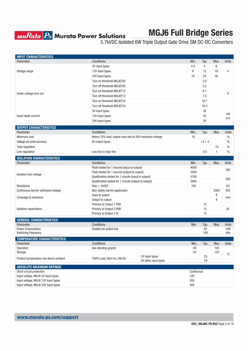
INPUT CHARACTERISTICS
Parameter Conditions Min. Typ. Max. Units
Voltage range
5V input types 4.5 5 9
V12V input types 9 12 18
24V input types 18 24 36
Under voltage lock out
Turn on threshold MGJ6T05 3.8
V
Turn off threshold MGJ6T05 3.2
Turn on threshold MGJ6T12 8.1
Turn off threshold MGJ6T12 7.5
Turn on threshold MGJ6T24 16.7
Turn off threshold MGJ6T24 16.3
Input ripple current
5V input types 30mA p-p
12V input types 45
24V input types 30
OUTPUT CHARACTERISTICS
Parameter Conditions Min. Typ. Max. UnitsMinimum load Below 10% load, output may rise to 30V maximum voltage 10 %
Voltage set point accuracy All output types +3 / -2 %
Total regulation 10 %
Line regulation Low line to high line 0.5 1 %
ISOLATION CHARACTERISTICS
Parameter Conditions Min. Typ. Max. Units
Isolation test voltage
Flash tested for 1 second (input to output) 4000VAC
Flash tested for 1 second (output to output) 2500Qualification tested for 1 minute (input to output) 5700
VDCQualification tested for 1 minute (output to output) 3000
Resistance Viso = 1kVDC 100 GΩContinuous barrier withstand voltage Non-safety barrier application 3000 VDC
Creepage & clearanceInput to output 8
mmOutput to output 8
Isolation capacitancePrimary to Output 1 VHA 15
pFPrimary to Output 2 VHB 15Primary to Output 3 VL 15
GENERAL CHARACTERISTICS
Parameter Conditions Min. Typ. Max. UnitsPower Consumption Disable pin pulled low 45 mWSwitching frequency 100 kHz
TEMPERATURE CHARACTERISTICS
Parameter Conditions Min. Typ. Max. UnitsOperation See derating graphs -40 105
°CStorage -55 125
Product temperature rise above ambient 100% Load, Nom VIN, Still Air5V input types 25All other input types 19
ABSOLUTE MAXIMUM RATINGS
Short-circuit protection ContinuousInput voltage, MGJ6 5V input types 12VInput voltage, MGJ6 12V input types 20VInput voltage, MGJ6 24V input types 40V

MGJ6 Full Bridge Series5.7kVDC Isolated 6W Triple Output Gate Drive SM DC-DC Converters
KDC_MGJ6C-FB.B02 Page 3 of 14
www.murata-ps.com/support
TECHNICAL NOTES
ISOLATION VOLTAGE
‘Hi Pot Test’, ‘Flash Tested’, ‘Withstand Voltage’, ‘Proof Voltage’, ‘Dielectric Withstand Voltage’ & ‘Isolation Test Voltage’ are all terms that relate to the same thing, a test voltage, applied for a specified time, across a component designed to provide electrical isolation, to verify the integrity of that isolation.
Murata Power Solutions MGJ6 series of DC-DC converters are all 100% production tested at 4kVACrms for 1 second from input to output and 2.5kVACrms for 1 second from output to output. Also they are all qualification tested at 5.7kVDC for 1 minute from input to output and 3kVDC for 1 minute from output to output.
A question commonly asked is, “What is the continuous voltage that can be applied across the part in normal operation?”
When the insulation in the MGJ6 series is not used as a safety barrier , i.e. provides functional isolation only, continuous or switched voltages across the barrier up to 3kV are sustainable. Long term reliability testing at these voltages continues. Peak Inception voltages measured were in excess of 3.5kV when testing for partial dis-charge in accordance with IEC 60270. Please contact Murata for further information.
The MGJ6 series is pending recognition by Underwriters Laboratory to 250 Vrms Reinforced Insulation, please see safety approval section below.
REPEATED HIGH-VOLTAGE ISOLATION TESTING
It is well known that repeated high-voltage isolation testing of a barrier component can actually degrade isolation capability, to a lesser or greater degree depending on materials, construction and environment. We therefore strongly advise against repeated high voltage isolation testing, but if it is absolutely required, that the voltage be reduced by 20% from specified test voltage.
SAFETY APPROVAL
ANSI/AAMI ES60601-1
The MGJ6 series is pending recognition ANSI/AAMI ES60601-1.
UL 60950
The MGJ6 series is pending recognition by Underwriters Laboratory (UL) to UL 60950 for reinforced insulation to a working voltage of 250Vrms with a maximum measured product operating temperature of 105°C.
Creepage and clearance 8mm, input to output & across outputs.
FUSING
The MGJ6 Series of converters are not internally fused so to meet the requirements of UL an anti-surge input line fuse should always be used with ratings as defined below. Input Voltage, 5V 4AInput Voltage, 12V 2AInput Voltage, 24V 1AAll fuses should be UL recognized, 250Vac rated.
CHARACTERISATION TEST METHODS
Ripple & Noise Characterisation Method
Ripple and noise measurements are performed with the following test configuration.
C1 1μF X7R m ultilayer ceramic capacitor, voltage rating to be a minimum of 3 times the output voltage of the DC-DC converter
C2 10μF tantalum capacitor, voltage rating to be a minimum of 1.5 times the output voltage of the DC-DC converter with an ESR of less than 100mΩ at 100 kHz
C3 100nF multilayer ceramic capacitor, general purposeR1 450Ω resistor, carbon film, ±1% toleranceR2 50Ω BNC terminationT1 3T of the coax cable through a ferrite toroidRLOAD Resistive load to the maximum power rating of the DC-DC converter. Connections should be made via twisted wiresMeasured values are multiplied by 10 to obtain the specified values.
Differential Mode Noise Test SchematicOSCILLOSCOPE Y INPUT
SUPPLY
C1 C2 C3 R1 T1 R2
Input Output
DC/DC Converter
R LOAD
+ +
-
-

MGJ6 Full Bridge Series5.7kVDC Isolated 6W Triple Output Gate Drive SM DC-DC Converters
KDC_MGJ6C-FB.B02 Page 4 of 14
www.murata-ps.com/support
EFFICIENCY VS LOAD
MGJ6T05F24MC MGJ6T12F24MC
MGJ6T24F24MC
RoHS COMPLIANCE, MSL AND PSL INFORMATION
This series is compatible with Pb-Free soldering systems and is also backward compatible with Sn/Pb soldering systems. The MGJ6 full bridge series has a process, moisture, and reflow sensitivity classification of MSL2 PSL R7F as defined in J-STD-020 and J-STD-075. This translates to: MSL2 = 1 year floor life, PSL R7F = Peak reflow temperature 245°C with a limitation on the time above liquidus (217°C) which for this series is 90sec max. The pin termination finish on this product series is Gold with Nickel Pre-plate.
0
10
20
30
40
50
60
70
80
90
10 20 30 40 50 60 70 80 90 100
Effic
ienc
y (%
)
Load (%)
0
10
20
30
40
50
60
70
80
90
10 20 30 40 50 60 70 80 90 100
Effic
ienc
y (%
)
Load (%)
0
10
20
30
40
50
60
70
80
90
10 20 30 40 50 60 70 80 90 100
Effic
ienc
y (%
)
Load (%)

MGJ6 Full Bridge Series5.7kVDC Isolated 6W Triple Output Gate Drive SM DC-DC Converters
KDC_MGJ6C-FB.B02 Page 5 of 14
www.murata-ps.com/support
DERATING GRAPHS
Derating curves are based on IPC-9592. With no derating some components may be operating at the manufacturers maximum temperature ratings.
MGJ6T05F24MC
MGJ6T12F24MC
MGJ6T24F24MC
0
10
20
30
40
50
60
70
80
90
100
70 75 80 85 90 95 100 105
Load
(%)
Temperature (°C)
Low Vin
Nom and High Vin
100 LFM Low Vin
100 LFM Nom and High Vin200 LFM All Vin
0
10
20
30
40
50
60
70
80
90
100
70 75 80 85 90 95 100 105
Load
(%)
Temperature (°C)
Low and Nom Vin
High Vin
100 LFM All Vin
0
10
20
30
40
50
60
70
80
90
100
70 75 80 85 90 95 100 105
Load
(%)
Low Vin
Nom Vin
High Vin
Low and Nom Vin, 100LFMLow Vin, 200LFM
High Vin, 100LFM
Nom Vin, 200LFM
High Vin, 200LFM
Low Vin, 400LFM
Nom and High Vin, 400LFM

MGJ6 Full Bridge Series5.7kVDC Isolated 6W Triple Output Gate Drive SM DC-DC Converters
KDC_MGJ6C-FB.B02 Page 6 of 14
www.murata-ps.com/support
EMC FILTERING AND SPECTRA
FILTERING
MGJ6T05F24MC (Quasi Peak) MGJ6T05F24MC (Average)
MGJ6T12F24MC (Quasi Peak) MGJ6T12F24MC (Average)
C1, C2 & C3 Polyester or ceramic capacitor
C4 Electrolytic capacitor (note R1 could be omitted if C4 has ESR >= R1)
DC
DCL1
+VIN
-VIN
C1
C4C3
C2 R1 +VOUT
-VOUT
TO MEET CURVE BPart Number C1 L1 Part Number C2 C3 R1 C4
MGJ6T05F24MC 10μF 1mH 51105C 1nF 1nF 1Ω 470μFMGJ6T12F24MC 10μF 1mH 51105C 1nF 1nF 1Ω 470μFMGJ6T24F24MC 10μF 1mH 51105C 1nF 1nF 1Ω 470μF
The following filter circuit and filter table shows the input filters typically required to meet conducted emissions limits for EN 55022 curve B using Quasi-Peak (pink line) and average (green line) detectors according to CISPR22. The following plots show measurements of the positive (L1) and negative (L2) inputs for both Quasi-peak limit B adher-ence and Average limit B adherence. If a high dv/dt above 80kV/us is expected from output to input it is advised that a common mode filter is used on each output as this will reduce the common mode current circulating between outputs and input and causing interference.
0
10
20
30
40
50
60
70
80
1.00E+05 1.00E+06 1.00E+07 1.00E+08
dBuV
Frequency (Hz)
0
10
20
30
40
50
60
70
80
1.00E+05 1.00E+06 1.00E+07 1.00E+08
dBuV
Frequency (Hz)
0
10
20
30
40
50
60
70
80
1.00E+05 1.00E+06 1.00E+07 1.00E+08
dBuV
Frequency (Hz)
0
10
20
30
40
50
60
70
80
1.00E+05 1.00E+06 1.00E+07 1.00E+08
dBuV
Frequency (Hz)

MGJ6 Full Bridge Series5.7kVDC Isolated 6W Triple Output Gate Drive SM DC-DC Converters
KDC_MGJ6C-FB.B02 Page 7 of 14
www.murata-ps.com/support
EMC FILTERING AND SPECTRA
MGJ6T24F24MC (Quasi Peak) MGJ6T24F24MC (Average)
0
10
20
30
40
50
60
70
80
1.00E+05 1.00E+06 1.00E+07 1.00E+08
dBuV
Frequency (Hz)
0
10
20
30
40
50
60
70
80
1.00E+05 1.00E+06 1.00E+07 1.00E+08
dBuV
Frequency (Hz)

MGJ6 Full Bridge Series5.7kVDC Isolated 6W Triple Output Gate Drive SM DC-DC Converters
KDC_MGJ6C-FB.B02 Page 8 of 14
www.murata-ps.com/support
APPLICATION NOTES
Start-up times
Part No.Start-up times
msMGJ6T05F24MC 30MGJ6T12F24MC 30MGJ6T24F24MC 30
Disable/Frequency synchronisation
Min Typ Max Units
Disable/Synch(Pin is active low)
Pull Down Current 0.5 mAInput High 2 5 VInput Low 0 0.8 V
SynchronisationFrequency Range 90 100 110 kHz
Duty Cycle 25 75 %
Output configurations for power switches
Component IGBT SIC MOSFET
Zener diode1 9V1 5V1 9V1
Resistor 15K 18K 15K
Typical start up times for this series, with recommended maximum additional output capacitance are:
Output capacitance must not exceed:
Please refer to application notes for further information.
The Disable/Synchronization pin has three modes:
1. When a dc logic low voltage is applied to this pin the MGJ6 is disabled and enters a low quiescent current sleep mode.2. When this pin is left floating or a dc logic high (CMOS/TTL compatible) voltage is applied the MGJ6 is enabled and operates at the programmed frequency of 100kHz. 3. When a square wave of between 90kHz and 110kHz is applied to this pin, the switcher operates at the same frequency as the square wave. The falling edge of the square wave corresponds to the start of the switching cycle. If the signal is slower than 25Hz, it will be interpreted as enabling and disabling the part. If the MGJ6 is disabled, it must be disabled for 7 clock cycles before being re-enabled.
The DIS/Sync pin is a high impedance TTL input and can be triggered by noise from external circuits if not treated carefully. It is advised that any pcb traces connected to the DIS/Sync pin are kept as short as possible and away from other noisy pcb traces. The track should follow a similar route to the return path to avoid differential noise pick up. If the pin is not used for synchronisation then a 22nF capacitor can be added from DIS/Sync pin to –Vin to suppress noise.
1. Suggested zener diode is BZX84C.
There are several zener based divider circuits that can be used to configure a bipolar output for gate drives as shown below. The table below shows suggested component values for various power switches using circuit A.
+24V
0V
0V
+Vgate
-Vgate
+24V
0V
0V
+Vgate
-Vgate
GATEDRIVER
Vdd
Vss
Out
+24V
0V
IGBT
A B C
Output VoltageMaximum output
capacitanceV μF
24 VHA 2724 VHB 2724 VL 56

MGJ6 Full Bridge Series5.7kVDC Isolated 6W Triple Output Gate Drive SM DC-DC Converters
KDC_MGJ6C-FB.B02 Page 9 of 14
www.murata-ps.com/support
APPLICATION NOTES (Continued)
Schematic for driving IGBT
HI P
WM
DRI
VE A
+Vin
9
-Vin
8
DIS
/SYN
C 1
LO P
WM
DRI
VE C
7 VL
RTN
6VL
+24V
4 VH
B RT
N
5 VH
B +2
4V
2 VH
A R
TN
3VH
A +
24V
R3
R2
R4C1 C2
D3
D1
D2
Q3
R1
Q2
R8
R7
R5C3 C4
D6
D4
D5
Q4
R6
Q6
Q5
Q8
Q1
Q11
R15
D12
D11
Q12
R14
R13
C8R1
6
D10
C7
HI P
WM
DRI
VE B
LO P
WM
DRI
VE D
R10
D7
D8
Q7
Q9
R12
C5R9 D
9C6
R11
The following circuit shows an example of a complete full bridge and how the DC-DC would be connected using the zener divider in circuit A (page 8).

MGJ6 Full Bridge Series5.7kVDC Isolated 6W Triple Output Gate Drive SM DC-DC Converters
KDC_MGJ6C-FB.B02 Page 10 of 14
www.murata-ps.com/support
APPLICATION NOTES (Continued)
For convenience the three isolated 24V outputs have been labelled VHA (Voltage A for high side), VHB (Voltage B for high side), and VL (Voltage for low side) however they can be swapped if this helps to improve system layout. It is recommended however that if VHA or VHB are used in place of VL that an additional 4.7uF ceramic capacitor is added close to the output pins to reduce ripple voltage.Any output can be connected in parallel with another and all three outputs can also be connected in series with one another. With the possibility of series and parallel output connections a number of output configurations are possible. Some are shown below:A) 24V @ 0.25A B) 72V @ 0.083A outputC) 72V @ 0.028A, 48V @0.042A and 24V @ 0.083AD) +48V/-24V @ 0.083AE) Non-isolated +24V to +96V boost converter @0.083AF) Non-isolated +12V to +84V boost converter @0.083A
+Vin
9
-Vin
8
DIS
/SYN
C 1
7 VL
RTN
6VL
+24V
4 VH
B RT
N
5 VH
B +2
4V
2 VH
A R
TN
3VH
A +
24V
+24V
0.2
5A
0V
+Vin
9
-Vin
8
DIS
/SYN
C 1
7 VL
RTN
6VL
+24V
4 VH
B RT
N
5 VH
B +2
4V
2 VH
A R
TN
3VH
A +
24V
+72V
0.0
83A
0V
+Vin
9
-Vin
8
DIS
/SYN
C 1
7 VL
RTN
6VL
+24V
4 VH
B RT
N
5 VH
B +2
4V
2 VH
A R
TN
3VH
A +
24V
+24V
0.0
28A
+Vin
9
-Vin
8
DIS
/SYN
C 1
7 VL
RTN
6VL
+24V
4 VH
B RT
N
5 VH
B +2
4V
2 VH
A R
TN
3VH
A +
24V
+48V
0.0
83A
+Vin
9
-Vin
8
DIS
/SYN
C 1
7 VL
RTN
6VL
+24V
4 VH
B RT
N
5 VH
B +2
4V
2 VH
A R
TN
3VH
A +
24V
+96V
0.0
83A
48V
0.04
2A
24V
0.08
3A
0V -24V
0.0
83A
A)
B)C)
F)E)
D)
0V
7 VL
RTN
+Vin
9
-Vin
8
DIS
/SYN
C 1
7 VL
RTN
6VL
+24V
4 VH
B RT
N
5 VH
B +2
4V
2 VH
A R
TN
3VH
A +
24V
+84V
0.0
83A
0V7
VL R
TN
+12V
in 0V0V
0V
Note: Any single 24V output can deliver up to 3W however the output power from all outputs combined must not exceed 6W

MGJ6 Full Bridge Series5.7kVDC Isolated 6W Triple Output Gate Drive SM DC-DC Converters
KDC_MGJ6C-FB.B02 Page 11 of 14
www.murata-ps.com/support
APPLICATION NOTES (Countined)
SLIC Circuits
The output configuration shown below could be used for subscriber line interface circuits (SLIC’s), particularly for the Integrated Services Digital Network (ISDN) and also for standard telecommunications circuits where a local power source is preferred to the telephone system power due to either the power quality of the telecommunications system power supply or to avoid potential power line disturbances, such as lightning strikes and access switching, which will affect the target circuit function.Another application area is in fibre-in-the-loop (FITL) or radio-in-the-loop (RITL) interfacing via a standard telecommunication SLIC, where the usual telecommunication bat-tery voltage is not available due to the transmission media in use (fibre or radio). In particular, FITL/RITL interfaces directly on PC cards, in local monitor and boost circuits and at exchanges between the fibre/radio and wire media. The supply rails can be used for ringing generators as well as SLIC circuits or where both are combined, such as in the AMD AM79R79 Ringing SLIC device (see figure 2). The -72V rail is used primarily for the generation of the ringing signal (VBAT1), the -48V rail is used to supply in line access circuitry (VBAT2) and the -24V supply for the on-chip regulator for the logic interface (VNEG). Alternative devices from other manufacturers could use the -24V output for their internal circuit supply and -72V for ringing.
DC
DC
+Vin
-Vin 0V-24V
-48V
-72V VBAT1
VBAT2
VNEG
BGND
A
B
TIP
RING
AMD (Am7R79)
DIS/SYNC

MGJ6 Full Bridge Series5.7kVDC Isolated 6W Triple Output Gate Drive SM DC-DC Converters
KDC_MGJ6C-FB.B02 Page 12 of 14
www.murata-ps.com/support
APPLICATION NOTES (Continued)
Schematic for Powering Three Phase Drivers on Electrical Vehicle Systems
HI P
WM
DRI
VE A
+Vin
9
DIS
/SYN
C 1
-Vin
8
LO P
WM
DRI
VE D
+Vin
9
DIS
/SYN
C 1
-Vin
8
3 VH
A +
24V
2 VH
A R
TN
5 VH
B +2
4V
4 VH
B RT
N
6 VL
+24
V
7 VL
RTN
3 VH
A +
24V
2 VH
A R
TN
5 VH
B +2
4V
4 VH
B RT
N
6 VL
+24
V
7 VL
RTN
R1
R2
R4R3
C1 C2D
3
Q3
Q2
D2
D1
Q1
R8
R7
R5R6
C3 C4D
6
Q4
Q6
D5
D4
Q5
R20
R19
R17
R18
C9 C10
D15
Q13
Q15
D14
D13
Q14
R21
R22
R24
R23
C12
C11
D16
Q18
Q16
D27
D18
Q17
R13
R14
R16
R15
C8 C7D
10
Q12
Q10
D11
D12
Q11
R12
R11
R24
R10
C5 C3D
9
Q7
Q9
D7
Q8
D8
HI P
WM
DRI
VE B
LO P
WM
DRI
VE E
HI P
WM
DRI
VE C
LO P
WM
DRI
VE F
For three phase drives on an Electric Vehicle system it is sometimes necessary, for safety and diagnostic reasons to power the high side switches independently to the Low side switches. This means that if a fault occurs on a the high side switch it is possible to disable all of the high side switches without disabling the low side switches. The circuit below shows how two Full bridge MGJ6 units can be connected to achieve this.

MGJ6 Full Bridge Series5.7kVDC Isolated 6W Triple Output Gate Drive SM DC-DC Converters
KDC_MGJ6C-FB.B02 Page 13 of 14
www.murata-ps.com/support
PACKAGE SPECIFICATIONS
MECHANICAL DIMENSIONS PIN CONNECTIONS
Pin Function
1 Dis/Sync
2 VHA RTN
3 VHA +24V
4 VHB RTN
5 VHB +24V
6 VL +24V
7 VL RTN
8 -Vin
9 +Vin
RECOMMENDED FOOTPRINT DETAILS
All dimensions in mm (inches), Controlling dimensions is mm. Tolerance (unless otherwise stated) ±0.25 (0.010). Component layout is shown for reference only Weight: 17.3g
1 2 3
6789
11.05±0.25 [0.435±0.010]
21.59±0.25 [0.850±0.010]26.62±0.25 [1.048±0.010]
1.17±0.25 [0.046±0.010]
1.52±0.30 [0.060±0.012]
19.5
6±0.
35 [0
.770
±0.0
14]
x9 PINS2.29±0.08 [0.090±0.003]
x9 PINS 1.60±0.05 [0.063±0.002]
41.53±0.15 [1 .635±0.006]
22.6
1±0.
15 [0
.890
±0.0
06]
SMA PICKUP POINT(TOP OF CORE)
13.85±0.50 [0 .545±0.020]
0.10 S
S
SEATING PLANE 14.0
5±0.
50 [0
.553
±0.0
20]
x9 PINS
4
5
39.19±0.25 [1.543±0.010]
SMA PICK UP POINT
(15.00 [0.591])
11.05 [0.435]
21.59 [0.850]
x9 PLACES3.38 [0.133]
x9 PLACES 2.41 [0.095]
RECOMMENDED ISOLATION BARRIER
26.62 [1.048]39.19 [1.543]
8.50 [0.335]
8.50
[0.3
35]
19.5
6 [0
.770
]

MGJ6 Full Bridge Series5.7kVDC Isolated 6W Triple Output Gate Drive SM DC-DC Converters
KDC_MGJ6C-FB.B02 Page 14 of 14
www.murata-ps.com/support
Murata Power Solutions, Inc. makes no representation that the use of its products in the circuits described herein, or the use of other technical information contained herein, will not infringe upon existing or future patent rights. The descriptions contained herein do not imply the granting of licenses to make, use, or sell equipment constructed in accordance therewith. Specifications are subject to change without notice. © 2018 Murata Power Solutions, Inc.
This product is subject to the following operating requirements
and the Life and Safety Critical Application Sales Policy:
Refer to: http://www.murata-ps.com/requirements/
TAPE & REEL SPECIFICATIONS
REEL OUTLINE DIMENSIONS REEL PACKAGING DETAILS
TAPE OUTLINE DIMENSIONS
DIRECTION OF UNREELING
56.0
[2.2
05]
4.0 [0.157]
36.0 [1.417]
15.5 [0.610]
26.2
[1.0
31]
COVER TAPE
52.4
[2.0
63]
42.0
[1.6
53]#
23.1 [0.908]#
Product Orientation
Pin 1, located nearest to carrier drive sprocket.
Reel Quantity: 7” 23 - or 13” - 92
Tape & Reel specifications shall conform with current EIA-481 standardUnless otherwise stated all dimensions in mm(inches) ±0.1mm (±0.004 Inches)Controlling dimension is mmComponents shall be orientated within the carrier tape as indicated# Measured on a plane 0.3mm above the bottom pocket
Tape & Reel specifications shall conform with current EIA-481 standardUnless otherwise stated all dimensions in mm(inches) Controlling dimension is mm# Measured at hub## Six equi-spaced slots on 180mm/7” reel
50.4 [1.984]MAX #
Ø13.512.8 [Ø 0.531
0.504 ]
1.5 [0.059]MIN ##
Ø20.2 [Ø0.795]MIN
Ø330 [13.000]OR
Ø177.8 [7.000]
100 [3.937]MIN
LEADER SECTION400 [15.748] MIN
GOODSENCLOSURE
SECTION
TRAILER SECTION160 [6.299] MIN