methods of synthesis and characterization of ...cs.stanford.edu/people/jlhiatt/thesis.pdf ·...
TRANSCRIPT

Methods of Synthesis and Characterization of Nanostructures Bridged By Single
Molecules
An Undergraduate Honors Thesis
Presented to
The Department of Physics
Stanford University
In Partial Fulfillment
of the Requirements for the Degree
Bachelor of Science in Physics with Departmental Honors
Jeremy L. Hiatt
June 2008

Acknowledgements
I would like to thank Professor Goldhaber-Gordon for agreeing to be my honorsadvisor, as well as for allowing me to join his group in the first place. I would alsolike to express my gratitude to Professor Chidsey for reading my thesis and providingnumerous pieces of helpful advice along the way. Thanks also to Alex Neuhausen,the graduate student whose project I joined last spring, as well as the rest of themembers of the Goldhaber-Gordon and Chidsey groups, who tolerated my presence.
I’d also like to thank Menesha Mannapperuma for her unvarnished critiques andunwavering support, as well as my friends Amos, Colin, Owen, and Mary. Finally,I would like to thank Rick Pam, Elva Carbajal, and the Physics Department as awhole for supporting my research enthusiastically, and of course financially.

Preface
I was invited to join this project in April, 2007 by Alex Neuhausen, a graduate studentin the Goldhaber-Gordon group. Alex was my mentor, teaching me various techniquesand showing me around the lab. Much of the work documented in this thesis wasperformed in close collaboration with him. Alex took the lead on most aspects of theproject, especially in the area of fabrication. I certainly had some input in those areasbeyond performing rote tasks. For example, I helped to develop an image processingprotocol that converted pictures taken in an optical microscope to a pattern for theSEM.
I was more involved with the chemistry aspects of the project. Last summer, Ispent a fair amount of time working on the resin-based “click” method, trying toget it to work. I experimented with many different solvents, trying to find one thatwould swell the resin to the point where the nanoparticles could penetrate the resin.When I decided to pursue an honors thesis, I was planning on performing the linkingreaction with alternate ligands, like diamines. When it failed to work out after a fewattempts, and in a similar manner to the failure of the dithiol, I put that projecton hold to help Alex get the dithiol linking to work. I spent a fair amount of timetrying various phase transfer schemes, hoping to find a viable way to disperse colloidin organic solvent that didn’t involve coating the nanoparticles in a thiol monolayer.In summary, I was more autonomous when I was working on the chemistry side ofthe project, though I felt like I also contributed a fair share to the fabrication andother aspects of the “physics” side.

Table of Contents
Introduction . . . . . . . . . . . . . . . . . . . . . . . . . . . . . . . . . . . 1
Chapter 1: Literature Review . . . . . . . . . . . . . . . . . . . . . . . . 31.0.1 Mechanisms of Electron Transport . . . . . . . . . . . . . . . 4
1.1 Solution-Phase Measurements of Single-Molecule Conductance . . . . 61.1.1 Probing Self-Assembled Monolayers . . . . . . . . . . . . . . . 71.1.2 Mechanical Break Junctions with STM . . . . . . . . . . . . . 8
1.2 Solid-State Single-Molecule Devices . . . . . . . . . . . . . . . . . . . 101.2.1 Solid-State Mechanical Break Junctions . . . . . . . . . . . . . 101.2.2 Fabrication of Gaps by Electromigration . . . . . . . . . . . . 111.2.3 Nanoparticle-based Devices . . . . . . . . . . . . . . . . . . . 13
1.3 Multi-molecule Electronic Devices and Applications . . . . . . . . . . 151.3.1 Sandwiched SAM devices . . . . . . . . . . . . . . . . . . . . . 15
Chapter 2: Direct Approach to Dimer Synthesis . . . . . . . . . . . . . 192.1 Introduction . . . . . . . . . . . . . . . . . . . . . . . . . . . . . . . . 19
2.1.1 Establishing Electrical Contact to Nanoparticles . . . . . . . . 202.1.2 Synthesizing Dimers by Direct Addition of Linker Molecule . . 23
2.2 Characterization of the Dimer Mixes . . . . . . . . . . . . . . . . . . 232.3 Tweaking the Recipe . . . . . . . . . . . . . . . . . . . . . . . . . . . 262.4 Possible Modes of Failure . . . . . . . . . . . . . . . . . . . . . . . . . 282.5 Gold Colloid in Organic Solvent: Synthesis vs. Phase Transfer . . . . 302.6 Alternate Ligands . . . . . . . . . . . . . . . . . . . . . . . . . . . . . 31
Chapter 3: The “Click” Approach . . . . . . . . . . . . . . . . . . . . . . 343.1 Resin Approach: Single-Molecule Functionalization . . . . . . . . . . 353.2 Functionalization/Characterization of the Nanoparticles with Hetero-
geneous Monolayers . . . . . . . . . . . . . . . . . . . . . . . . . . . . 363.3 Clicking the Nanoparticles Together . . . . . . . . . . . . . . . . . . . 37
Future Directions . . . . . . . . . . . . . . . . . . . . . . . . . . . . . . . . 384.1 Will Processing Damage the Molecule? . . . . . . . . . . . . . . . . . 38
4.1.1 Metallized DNA . . . . . . . . . . . . . . . . . . . . . . . . . . 39
Appendix A: Experimental Methods . . . . . . . . . . . . . . . . . . . . 41

A.1 Gold Colloid in Organic Solvent . . . . . . . . . . . . . . . . . . . . . 41A.1.1 Synthesis . . . . . . . . . . . . . . . . . . . . . . . . . . . . . 41A.1.2 Phase Transfer . . . . . . . . . . . . . . . . . . . . . . . . . . 41
A.2 Dimer Mixes . . . . . . . . . . . . . . . . . . . . . . . . . . . . . . . . 42A.2.1 Preparation . . . . . . . . . . . . . . . . . . . . . . . . . . . . 42A.2.2 Deposition Process . . . . . . . . . . . . . . . . . . . . . . . . 42
A.3 Fabrication of Contacts . . . . . . . . . . . . . . . . . . . . . . . . . . 43A.4 The “Click” Process . . . . . . . . . . . . . . . . . . . . . . . . . . . 43
A.4.1 Functionalization of the Nanoparticles . . . . . . . . . . . . . 43A.4.2 Performing the “Click” Reaction . . . . . . . . . . . . . . . . 43
References . . . . . . . . . . . . . . . . . . . . . . . . . . . . . . . . . . . . . 44

List of Tables
2.1 Dimer counting data . . . . . . . . . . . . . . . . . . . . . . . . . . . 24

List of Figures
1 An overview of the scheme to contact single molecules through clickchemistry. From (1). . . . . . . . . . . . . . . . . . . . . . . . . . . . 2
1.1 The Aviram & Ratner rectifier. From (2). . . . . . . . . . . . . . . . 31.2 Predicted I-V and differential conductance traces for the BPD molecule.
From (3). . . . . . . . . . . . . . . . . . . . . . . . . . . . . . . . . . 51.3 Current-Voltage Characteristics of a Coulomb-Blockaded Device . . . 61.4 Schematic of a self-assembled monolayer on gold. From (4). . . . . . . 71.5 Mechanical break junctions with STM . . . . . . . . . . . . . . . . . 91.6 Conductance as a function of twist angle . . . . . . . . . . . . . . . . 101.7 Correlated Raman and Conductance Measurements . . . . . . . . . . 131.8 Trapping and measuring conductance of dimer structures . . . . . . . 141.9 Redox of the catenane molecule . . . . . . . . . . . . . . . . . . . . . 161.10 A molecular electronic memory array . . . . . . . . . . . . . . . . . . 18
2.1 Comparison of Regularity and Aspect Ratio of Contacting Methods . 192.2 Locating Dimers . . . . . . . . . . . . . . . . . . . . . . . . . . . . . 212.3 Contacted Monomers . . . . . . . . . . . . . . . . . . . . . . . . . . . 222.4 Structure of biphenyl dithiol . . . . . . . . . . . . . . . . . . . . . . . 232.5 Dimers visible during SEM inspection, highlighted by red circles. . . . 252.6 UV-vis spectrum of pH-adjusted colloid . . . . . . . . . . . . . . . . . 252.7 Colors of gold colloid . . . . . . . . . . . . . . . . . . . . . . . . . . . 262.8 Apparent Raman enhancement with a dimer . . . . . . . . . . . . . . 272.9 X-ray Structure of a Gold Nanoparticle . . . . . . . . . . . . . . . . . 292.10 Alternate ligands . . . . . . . . . . . . . . . . . . . . . . . . . . . . . 32
3.1 An overview of the steps in the resin-based “click” synthesis . . . . . 354.2 PMMA Outgassing Issues . . . . . . . . . . . . . . . . . . . . . . . . 394.3 Carbon nanotubes contacted by metallized DNA . . . . . . . . . . . . 40

Abstract
Nanostructures made of colloidal gold offer much promise in the field of molecular
electronics. One of the most basic examples of these structures is the dimer: a pair
of gold nanoparticles connected by a single molecule. Typical linker molecules are
functionalized on either end with thiol (-SH) groups, since sulfur has a high affinity
for gold surfaces. Recently published work presented conductance measurements of
single molecules, obtained by electrostatically trapping dimer structures onto gold
electrodes.
In this thesis I present several approaches to the synthesis of these dimer structures
by a dithiol linker molecule and discuss advantages and disadvantages of each method.
The simplest method is to directly add a dithiol linker molecule to gold colloid in
aqueous solution. However, insolubility of a typical linker molecule in pure water
necessitates a mixed-solvent environment, which can lead to false dimer formation.
An alternate scheme utilizes the azide-alkyne reaction of “click chemistry”, in
which an azide-functionalized molecule is joined with an alkyne-terminated molecule
by formation of a triazole ring structure. In this approach, the gold nanoparticles are
first coated with azide-terminated molecules; then, a diacetylene molecule (alkyne
groups on each end) is added to link together the azides. I present preliminary
characterization data and discuss the feasibility and possible future applications of
this approach.

Introduction
The overarching goal of this project is to establish reliable electrical contact to single
molecules, combining aspects of chemical synthesis with sophisticated lithography to
incorporate a single molecule into a macroscopic electrical circuit in order to measure
its conductance. This work falls into the broad category of “molecular electronics”,
where molecules take the place of traditional circuit elements in hopes of achieving
superior performance, scalability, and efficiency compared to semiconductor-based
counterparts.
The technique could have a wide variety of scientific applications in chemistry or
physics, and also as a screening technique for moletronics devices. Studying conduc-
tion through single molecules could give great insight into the properties of electrons
in that molecule. Alternatively, one could “fabricate” a quantum system with novel
properties in the form of a molecule and then test it using this technique. This
technique could also be used as a screening process to test properties of molecules
designed for practical application as memory elements, switches, etc. (1).
The following is a general overview of the scheme. The first step is to attach
gold nanoparticles to the ends of a target molecule in order to form a dumbbell-like
structure, commonly referred to as a dimer. Alternatively, the gold nanoparticles are
functionalized with a precursor to the final molecule, and synthetic chemistry joins
two particles together. The dimers are then deposited onto a substrate, and con-
ducting leads are patterned to contact each end. The device can then be probed for
conductance. The gold nanoparticles scale the end points of the molecule up to a size
that can be targeted with lithography. Gold nanoparticles are well suited for this pur-
pose in several respects. Gold colloid is readily commercially available in a wide size
range, and even some of the more exotic permutations are easy to synthesize. Also,
the process of binding molecules to gold surfaces has been extensively documented,
typically in the context of monolayer formation.
That being said, we have recently begun exploring an alternate scheme involv-
ing metallized DNA as a replacement for the nanoparticles. The ends of two DNA

Introduction 2
strands bind to the target molecule. These DNA strands are subsequently metal-
lized, converting them effectively into wires that are then contacted with patterned
leads. One major problem currently with metallized DNA is that the metal tends to
form numerous grains rather than a smooth, solid wire. Nevertheless, it remains an
attractive alternative to gold nanoparticles.
We found that our original recipe simply failed to produce dimers joined together
by a linker molecule, leading to a thorough investigation of why it wasn’t working. In
this thesis, I discuss the variations attempted on the basic approach, as well as intro-
duce an alternative strategy for dimer synthesis involving “click” chemistry. “Click”
chemistry is an approach to organic synthesis that makes use of a small number of
highly reliable reactions to link together chemical subunits (5). In this context, “click”
offers both simplicity as well as the means to build up complex structures from a few
basic subunits. I will present the current state of our attempts to use “click” to make
dimers.
Figure 1: An overview of the scheme to contact single molecules through click chem-istry. From (1).
Chapter 1
Literature Review
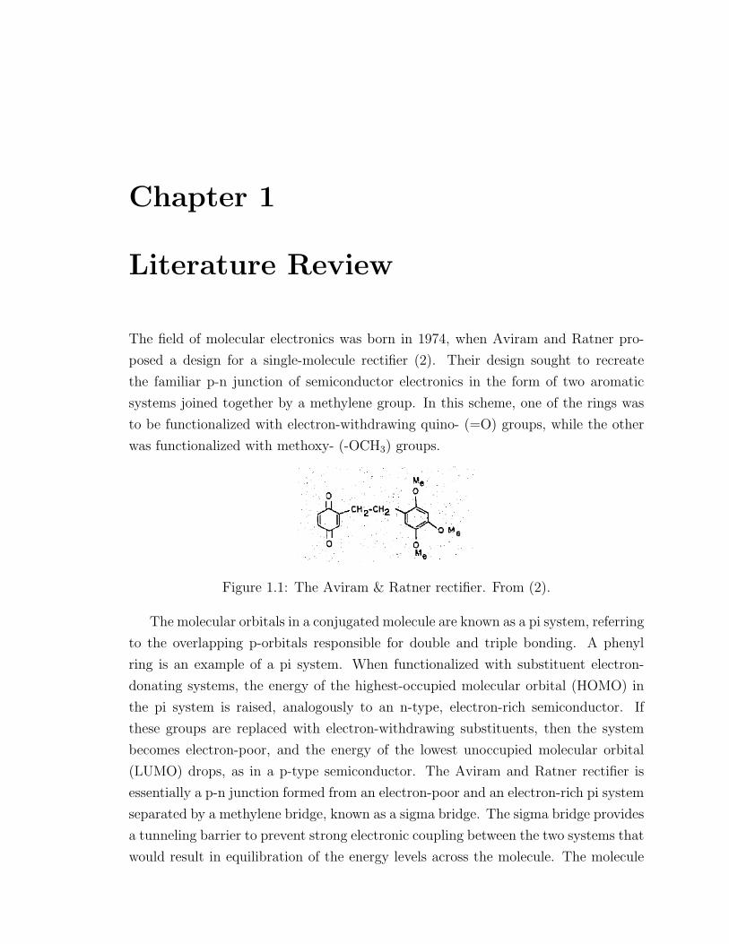
The field of molecular electronics was born in 1974, when Aviram and Ratner pro-
posed a design for a single-molecule rectifier (2). Their design sought to recreate
the familiar p-n junction of semiconductor electronics in the form of two aromatic
systems joined together by a methylene group. In this scheme, one of the rings was
to be functionalized with electron-withdrawing quino- (=O) groups, while the other
was functionalized with methoxy- (-OCH3) groups.
Figure 1.1: The Aviram & Ratner rectifier. From (2).
The molecular orbitals in a conjugated molecule are known as a pi system, referring
to the overlapping p-orbitals responsible for double and triple bonding. A phenyl
ring is an example of a pi system. When functionalized with substituent electron-
donating systems, the energy of the highest-occupied molecular orbital (HOMO) in
the pi system is raised, analogously to an n-type, electron-rich semiconductor. If
these groups are replaced with electron-withdrawing substituents, then the system
becomes electron-poor, and the energy of the lowest unoccupied molecular orbital
(LUMO) drops, as in a p-type semiconductor. The Aviram and Ratner rectifier is
essentially a p-n junction formed from an electron-poor and an electron-rich pi system
separated by a methylene bridge, known as a sigma bridge. The sigma bridge provides
a tunneling barrier to prevent strong electronic coupling between the two systems that
would result in equilibration of the energy levels across the molecule. The molecule

4
will theoretically “rectify” because it is much more likely for an electron to go from
the electron-rich system to the electron-poor than to travel in the reverse direction.
1.0.1 Mechanisms of Electron Transport
The mechanism for electron transport through a molecule is expected to depend
strongly on both the properties of the molecule itself as well as the nature of the
contacts (6). Possible schemes for contacting molecules include formation of chem-
ical bonds between the molecule and the electrodes (used in a wide variety of ap-
proaches: see following sections) or tunnel junctions across non-bonded contacts
(used in solution-phase STM as well as “sandwiched” monolayers). Depending on
the properties of the molecule and the contacts, there are several possible phenomena
that could occur. Some notable features of the various mechanisms are temperature
dependence (or lack thereof, in the case of pure tunneling), behavior at zero bias and
low bias, and dependence on gate voltage and applied magnetic field.
Resonant Tunneling One possible mechanism for transport is resonant tunneling
through the molecule. In 2003, Xue and Ratner modeled transport through phenyl
dithiol (PDT) and biphenyl dithiol (BPD) coupled chemically to metal electrodes
through the sulfur atoms (3). At low applied bias, the current is predicted to be
roughly linear with voltage, due to tunneling through the HOMO-LUMO gap. They
predicted that high applied bias would increase the energy of the HOMO, leading to
peaks in the conductance when an energy level lined up with the Fermi level in the
metal electrode. These levels are occupied states, corresponding to HOMO, HOMO
- 1, etc. See Figure 1.2.
Coulomb Blockade A common phenomenon in low temperature conductance mea-
surements is known a Coulomb blockade, which is manifested as a suppression of
differential conductance at zero bias. Coulomb blockade can arise in the simple case
of two electrodes separated by a tunnel barrier, or when an island sits between two
electrodes. In the case of electronic island states, it occurs when the charging energy
required to place another electron on the island exceeds the energy of a conduction
electron in the leads. The I-V curve shows characteristic stair step features, with
a jump each time another electronic state on the island lines up with the potential
energy of a conduction electron (see Figure 1.3). The gap between steps is determined
by the capacitance of the island. Another hallmark of Coulomb blockade is that it
can be tuned by adjusting a gate voltage. By modifying the electrostatic environ-

5
neling and thermionic emission contribution to the total cur-rent are shown. As expected, for tunneling transport througha large and thin barrier, the thermionic emission contributionto the current is negligible even at low bias !shown in theinsets". Since the variation of the thermionic emission con-tribution with bias voltage is small !in the coherent transportregime", this further reduces its contribution at high bias.Since this is the only temperature dependence in the coherent
transport model, we expect the temperature dependence of
the coherent current transport through the two molecules to
be weak !ignoring any disorder effects". Within the coherenttransport model, the thermionic emission and, correspond-
ingly, the temperature dependence of the current transport
can be important only if the barrier for electron transmission
is small and/or thick.
For comparison, we have also plotted the conductance-
voltage characteristics obtained using the equilibrium trans-
mission coefficient, i.e., replacing T(E ,V) in Eq. !12" withT(E ,V!0). Since the gold surface density of states are ap-proximately symmetric with respect to the Fermi level !thegold surface band around the Fermi level is due primarily to
the sp electrons", the difference between the G-V character-istics thus obtained and the self-consistent G-V characteris-
tics reflects the effect of the bias-induced modification of
molecular states.
For both molecules, only the low-bias conductance-
voltage characteristics !before reaching the first conductancepeak" can be reasonably well reproduced by the equilibriumtransmission characteristics. The deviation in both the mag-
nitude and the peak position of the conductance becomes
significant at large bias, there are also more conductance
peaks than would be obtained from the equilibrium transmis-
sion characteristics. So any attempt to predicting the nonlin-
ear transport characteristics from the equilibrium transmis-
sion characteristics combined with an assumption about the
voltage drop will lead to significant error. The effect of the
bias-induced modification of molecular states is also obvious
from looking at the shift of the frontier molecular levels by
the applied voltage, as shown in Fig. 16. The molecular lev-
els plotted are obtained by diagonalizing the molecular part
of the self-consistent Fock matrices at each bias voltage, i.e.,
the submatrix of HMM containing only the molecule itself
#since the molecular levels thus obtained do not include theeffect of self-energy induced shift, their values don’t match
the peaks in the PDOS or T(E ,V) plot shown later$. Themolecular levels are nearly constant at low voltages, but be-
gin to shift before reaching the first conductance peak. The
voltage at which the shift occurs corresponds to the voltage
where major deviation in the G-V characteristics occurs.
FIG. 14. I-V !upper figure"and G-V !lower figure" characteris-tics of the gold-PDT-gold device. The inset in the I-V plot gives the
magnified view at low bias. The dotted line in the G-V plot is
obtained assuming the transmission-energy relation to be bias inde-
pendent.
FIG. 15. I-V !upper figure" and G-V !lower figure" characteris-tics of the gold-BPD-gold device as in Fig. 14.
FIG. 16. Bias-induced modification of molecular levels at gold-
PDT-gold junction !left figure" and gold-BPD-gold junction !rightfigure". We have also shown the position of the equilibrium Fermi
level EF and the electrochemical potential of the two electrode
%L(R) in the plot.
YONGQIANG XUE AND MARK A. RATNER PHYSICAL REVIEW B 68, 115406 !2003"
115406-10Figure 1.2: Predicted I-V and differential conductance traces for the BPD molecule.From (3).
ment via the gate potential, one can bring the unoccupied electronic states in line
with the Fermi energy of the conduction electrons, thereby increasing conductance at
zero source-drain bias.
Other phenomena In other devices/molecules, the molecule may act as a pure
tunnel barrier, as in the case of “insulating” alkyl chains (6). In these cases, the
resistance increases exponentially with distance and is temperature-independent. Al-
ternatively, the conducting electrons can couple to vibrational modes of the molecule,
resulting in inelastic scattering (6).
Since the original work in 1974, much effort has been made to establish electrical
contact to single molecules. Recent efforts have focused on several main approaches
that fall into two broad categories: solution-phase measurements and fabrication of
solid-state single-molecule devices. Another class of solid-state devices seeks to exploit
the molecular electronic properties of a small collection of contacted molecules. Nearly
all of these techniques rely in some way on the gold-sulfur (Au-S) bond as a means of
contacting the macroscopic electrical setup to the molecular level, with a few notable
exceptions.

1.1. Solution-Phase Measurements of Single-Molecule Conductance 6
(a) I-V and Differential Conductance Curvesat Constant Gate Voltage
(b) Differential Conductanceat Varying Source-Drain andGate Voltages
Figure 1.3: I-V and differential conductance plots indicative of Coulomb blockade.(Left) Note the stair steps in the I-V curve, corresponding to peaks in differentialconductance. (Right) The diamond-like features are typical of Coulomb blockade.From (7).
1.1 Solution-Phase Measurements of Single-Molecule
Conductance
In a solution-phase measurement, the target molecule is present in bulk solution over
a surface, typically gold. In many cases, the measurement requires formation of a self-
assembled monolayer (SAM) on the gold surface. One of the most common examples
of a SAM, especially in this context, is a monolayer of alkanethiol on a gold surface.
See Figure 1.4 for a schematic diagram of a SAM. The favorable binding between
the sulfur and the surface gold atoms drives the molecules to form a close-packed
monolayer with the alkyl chains pointing out from the surface. A heterogeneous SAM
contains more than one type of molecule; in the case of conductance measurements,
usually a thiol with conjugated phenyl rings is present in low concentration relative
to a diluent alkyl thiol. However, since the hetero-interaction is less favorable than
the stacking of alkane chains, the inserted molecule will tend to accumulate at the
“grain boundaries” of the SAM, the interfaces of distinct packing domains.

1.1. Solution-Phase Measurements of Single-Molecule Conductance 7
Figure 1.4: Schematic of a self-assembled monolayer on gold. From (4).
1.1.1 Probing Self-Assembled Monolayers
Solution-phase measurements generally make use of high-resolution microscopy tech-
niques to make contact to a singe molecule, or maybe a few molecules. In 1996, Bumm
et al. demonstrated the conductivity of conjugated molecules relative to alkyl chains
(8). They used a scanning tunneling microscopy (STM) tip to probe a SAM of do-
decanethiol that was sparsely populated with a longer conjugated molecule. Though
they were able to show qualitatively that the conductance of the conjugated molecules
was, as expected, much higher than the conductance of the diluent molecules, they
could not make a quantitative assessment of the conductance because of the unknown
tunnel barrier between the STM tip and the molecule.
In 2001, Cui et al. reported the use of a similar technique with several key im-
provements. They formed monolayers of octanethiol interspersed with octanedithiol
and then introduced a population of gold nanoparticles. The free thiol groups in the
monolayer bound the nanoparticles, which were then located with a gold-coated, con-
ducting atomic force microscopy (AFM) tip (9). By pressing the tip into the nanopar-
ticle, they established electrical contact and constructed current-voltage (I-V) curves
for the dithiol. Compared to non-bonded octanethiol molecules, the conductance was
four orders of magnitude higher, demonstrating the conductivity of the Au-S bond.
However, this type of measurement suffers from complications due to the force re-
quired to contact the nanoparticle. In their report, they noted no variability in the
measured resistance of a bonded dithiol when varying the applied force. In contrast,
when making non-bonded contact the octanethiol monolayer, the authors observed
huge disparities in the resistance with varied force, probably due to rearrangement

1.1. Solution-Phase Measurements of Single-Molecule Conductance 8
of the molecules underneath. Also, the nanoparticle frequently contacted multiple
dithiol molecules, resulting in steeper I-V curves and lower observed resistance.
1.1.2 Mechanical Break Junctions with STM
An alternative to probing monolayers involves mechanically breaking point contacts
between an STM tip and a gold substrate in the presence of molecule. According
to the technique originally used to observe quantization of conductance in atomic-
size wires, a gold STM tip is driven into a gold surface and slowly retracted. When
the contact is stretched, the conductance is reduced in steps of G0, the fundamen-
tal conductance quantum. When only a single gold atom bridges the contact, the
conductance is G0 (11). This technique has been adapted to measure conductance
of single molecules by performing the retraction in a solution of the molecule of
interest. When a conducting molecule is present, a conductance well below G0 (usu-
ally about two orders of magnitude) is observed after the gold contact breaks. This
conductance similarly decreases stepwise, corresponding to a decreasing number of
molecules in the junction, until only a single molecule bridges the gap. The process is
repeated thousands of times to generate a statistical sample from which the conduc-
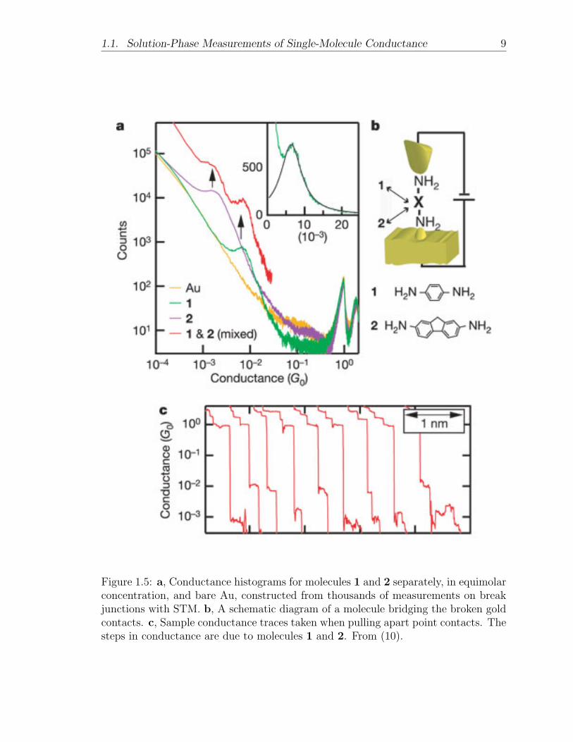
tance value is extracted. In a 2006 paper, Venkataraman et al. reported that while
dithiol molecules made poorly reproducible contact between the surface and STM
tip, diamine-functionalized molecules were found to have very well-defined conduc-
tance, in the form of strongly peaked samples (see Figure 1.5) (12). They attribute
this behavior to the selectivity of the gold-nitrogen bond. They claim that this bond
preferentially forms such that the molecule is perpendicular to the surface, the ideal
configuration for this type of measurement.
Venkataraman et al. published another paper later that year measuring conduc-
tance of substituted biphenyl molecules with distinct twist angles controlled by the
side groups on the rings. As expected, they observed a simple cosine-squared relation-
ship between conductance and twist angle (10). One of the major drawbacks of this
approach, and of solution-phase measurements in general, is that the measurement
cannot be performed at low temperature. It thus seems likely that thermal effects
will wash out interesting features. For example, the energy barrier for rotation of
a biphenyl molecule is small compared to kT at room temperature. In the paper
above, the authors predicted that the molecule would undergo many rotations during
the time of a single measurement, so even a single conductance trace for a single
molecule represents an average over the ensemble of configurations that the molecule
1.1. Solution-Phase Measurements of Single-Molecule Conductance 9
Figure 1.5: a, Conductance histograms for molecules 1 and 2 separately, in equimolarconcentration, and bare Au, constructed from thousands of measurements on breakjunctions with STM. b, A schematic diagram of a molecule bridging the broken goldcontacts. c, Sample conductance traces taken when pulling apart point contacts. Thesteps in conductance are due to molecules 1 and 2. From (10).

1.2. Solid-State Single-Molecule Devices 10
Figure 1.6: (a) Wire-frame models of the molecules used in this experiment, orderedby increasing twist angle and decreasing conductance. (b) Histograms taken fromthousands of conductance traces for each molecule, as well as bare gold. Coloredarrows indicate inferred conductance value for the corresponding molecule. (c) Plotshowing the approximate cosine-squared relation between conductance and twist an-gle. From (10).
can adopt. This limitation is probably the biggest drawback to solution-phase mea-
surements.
1.2 Solid-State Single-Molecule Devices
A solid-state measurement device is typically manufactured by first fabricating a pair
of electrodes separated by a nanometer-sized gap, then depositing a single molecule
within the gap to bridge the contacts. In most cases, they can be measured at
cryogenic temperatures, though they generally have low yield, and they permit fewer
repetitions of a measurement than solution-phase techniques.
1.2.1 Solid-State Mechanical Break Junctions
Several techniques exist for fabricating the narrow gaps needed for a solid-state device.
A 1997 paper from Reed et al. reported the use of a mechanically controlled break
junction to measure conductance (13). A gold wire was placed on a flexible substrate.
Flexing the substrate stretched and broke the wire into sharp points. Varying the
applied pressure to the substrate controlled the size of the gap. A solution of benzene-
1,4-dithiol was then introduced to form a monolayer on the contacts, and the gap size
was reduced until conductance was observed. The authors reported that conductance
increased stepwise with bias voltage reminiscent of Coulomb blockade behavior, with

1.2. Solid-State Single-Molecule Devices 11
the first step at ∼0.7 V and a corresponding resistance of ∼22 megohms. Occa-
sionally this first feature showed resistance of ∼14 megohms, which they attribute
to two molecules conducting in parallel. Since a resistance above 22 megohms was
never observed, this was reported to be the resistance of a single molecule. This
approach suffers from a few key drawbacks. The authors claim that only a single
molecule, or perhaps two, contributes to the conductance of the junction. Instead, a
more likely scenario is that one molecule strongly conducts, while many others are
weakly conducting in parallel. Also, the devices could not be gated. In recent years,
the technique has been refined so that the measurement could be performed at low
temperature and even with a gate electrode, though the problem of oddly shaped
contacts remains (14).
1.2.2 Fabrication of Gaps by Electromigration
Alternatively, nanometer-sized gaps can be formed by a process known as electromi-
gration. In this process, momentum transfer from conducting electrons to metal ions
leads to a concerted motion of these ions in the direction of the current, especially at
grain boundaries. Over time this effect can open gaps in a narrow wire. Long known
as a common source of failure in integrated circuits, electromigration was applied as
a fabrication technique in 1999 to produce nanometer-sized gaps (15). They reported
a high variability in the resistance, ranging from hundreds of kilohms to gigohms, of
the fabricated tunnel junctions, indicative of variations in the final separation width.
The gaps also tended to be non-uniform. Since then, techniques have improved to the
point where gaps can reliably be produced with a specific resistance and thus with a
specific width. Electromigrated gaps are commonly used as single-molecule contacts
because conduction through the gap is believed to take place in a molecule-sized vol-
ume, despite an aspect ratio that might seem to support many parallel channels for
electron transport. Electromigrated devices can also be probed at cryogenic temper-
atures. The devices can be back gated by applying a large voltage to the substrate,
potentially allowing manipulation of electrical properties of the gap.
These properties of electromigrated gaps have been exploited to explore a number
of single-molecule devices. In 2002, Park et al. observed Coulomb blockade as well as
Kondo effect in a single-atom transistor: a cobalt ion complex with variable-length
insulating tethers spanning an electromigrated gap (16). The characteristic feature
of Kondo effect is a peak in differential conductance at zero bias due to coupling
between a spin state on the island and the conduction electrons; it is split by an

1.2. Solid-State Single-Molecule Devices 12
applied magnetic field and suppressed at finite temperature. When attached with
longer tethers the molecule showed Coulomb blockade behavior, and Kondo effect
with shorter tethers. The Coulomb blockaded devices could be turned on at zero bias
by applying a gate voltage that varied from device to device. Nonblockaded resistance
varied by a factor of 10, ranging from ∼100 megohms up to 1 gigohm. This variability
was taken as evidence of single-molecule conductance. However, when back gating
a device with a given voltage, the electric field felt by the molecule can depend
strongly on its environment. In light of the large variation from device to device in
the shape of the contacts, it seems problematic to infer single-molecule conductance
from variability in this parameter. Yu and Natelson reported similar findings using
C60 as a single-molecule transistor within an electromigrated gap (17). For a very
small number of devices, manipulating the charge state of the molecule with applied
gate voltage would result in Kondo-like behavior. One of the major concerns with
electromigrated junctions is differentiating between behavior due to the presence of
a molecule and the intrinsic properties of the junction. Electromigration frequently
leads to formation of metal islands between the electrodes, which can give rise to
Coulomb blockade and Kondo behavior (18). Differentiating between conduction
through a molecule and tunneling to a metal island can thus be very challenging, and
this is one of the weak points of this approach. Another challenge is fabricating the
gap so that the minimum separation corresponds to the length of the target molecule.
Otherwise, it is easy to imagine how the molecule could bridge a wider area of the gap
and conduct in parallel with the small area that dominates tunneling current. While
gaps can be precisely fabricated for relatively small resistances, corresponding to small
separations, the resistance depends exponentially on separation distance. Thus the
technique does not scale well for the larger gaps necessary for longer molecules.
Despite these disadvantages, electromigrated gaps have been used to great ef-
fect to demonstrate qualitative behavior of single-molecule conductance. Keane et
al. observed hysteretic switching behavior in a three terminal single-molecule device
fabricated with electromigration (19). The operation of the device was very weakly
coupled to applied gate voltage, registering mild dependence in a few cases. These
results suggest the need for a stronger coupling to the molecule than back gating can
provide in order to reliably control conduction properties.
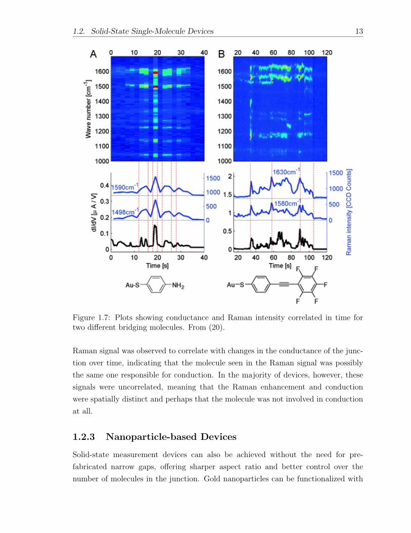
Electromigrated gaps have been found to be especially effective as hot spots
in surface-enhanced Raman spectroscopy (SERS). A recent paper from Ward et
al. reported simultaneous, correlated measurement of conduction and Raman response
within an electromigrated break junction (20). Approximately 10% of the time, the
1.2. Solid-State Single-Molecule Devices 13
Figure 1.7: Plots showing conductance and Raman intensity correlated in time fortwo different bridging molecules. From (20).
Raman signal was observed to correlate with changes in the conductance of the junc-
tion over time, indicating that the molecule seen in the Raman signal was possibly
the same one responsible for conduction. In the majority of devices, however, these
signals were uncorrelated, meaning that the Raman enhancement and conduction
were spatially distinct and perhaps that the molecule was not involved in conduction
at all.
1.2.3 Nanoparticle-based Devices
Solid-state measurement devices can also be achieved without the need for pre-
fabricated narrow gaps, offering sharper aspect ratio and better control over the
number of molecules in the junction. Gold nanoparticles can be functionalized with

1.2. Solid-State Single-Molecule Devices 14
thiol molecules a similar manner to the formation of a SAM on a gold substrate. Long
et al. demonstrated a method for assembling molecular junctions using nanoparticles
(21). In this scheme, silica nanoparticles were coated with nickel and gold films to ren-
der them magnetically susceptible and conducting. The gold surface was then coated
with various thiol-functionalized wire molecules expected to show good conductivity.
The nanoparticles were then trapped on magnetic pads, and I-V curves were con-
structed. Though this method cannot be applied to single-molecule measurements,
it is an example of a high-throughput, high-yield process to generate molecular junc-
tions.
(a) Dimer structuretrapped between contacts
(b) Conductance traces for various molecules
Figure 1.8: Trapped dimer approach to single-molecule conductance. (a) A dimertrapped between the contacts. Note the apparent presence of another dimer imme-diately adjacent. (b) Sample conductance traces for fully-conjugated 4,4’-biphenyldithiol (BPD), (4-mercaptophenyl)-ether (BPE), and 1,4-benzenedimethanethiol(BDMT). In the latter two molecules, conjugation is broken by additional functionalgroups. Note the peaks in the BPD trace: these would slide back and forth on thevoltage axis in time, but maintain a fixed spacing. From (22).
Most notably, Dadosh et al. reported single-molecule conductance using a nanoparticle-
based technique in 2005 (22). In this scheme, the target molecule was introduced to
a solution of nanoparticles in extremely low concentration (typically in a 1:10 ratio
of molecule to nanoparticle) so that the dimers formed would be bridged by exactly
one molecule. The mix was then centrifuged, causing differentiation into bands. Se-
lecting the proper band would yield a concentration of ∼50% dimers as a percentage
of total structures. These dimer structures were then electrostatically trapped by
applying an ac voltage to a set of gold electrodes, attracting the dimers to the con-
tacts. Once trapped, the sample was dried and cooled to cryogenic temperatures
for measurement. As with many of the other techniques discussed here, the yield of
working devices was quite low; even then, the results are plagued by high variability

1.3. Multi-molecule Electronic Devices and Applications 15
in observed conductance. When measuring conductance of biphenyl dithiol (BPD),
the highest conductivity molecule measured, the characteristic shape of the differen-
tial conductance plot was reproduced across all devices (see Figure 1.2.3). However,
the measured conductances varied by approximately an order of magnitude, and the
peaks would shift back and forth over time, which the authors attribute to random
gating due to changes in electrostatic environment. Finally, the observed conductance
for BPD was several orders of magnitude lower than predicted by theory. When con-
tacting a single gold nanoparticle, the junction resistance was typically 10 megohms,
likely due to the tunnel barrier formed by the protective citrate layer on the colloid.
This flaw adds complexity to the experimental system, since these leads could in
principle exhibit similar conduction properties to a single molecule, as with the metal
islands in electromigrated gaps. This concern leads to consideration of a larger issue:
one cannot devise a proper control experiment against which to compare the exper-
imental results. It is therefore imperative to demonstrate conclusively that a single
molecule is present within the gap. In principle, a nanoparticle-based measurement
technique offers some advantage over fabricated gaps, chiefly that it can be extended
to three, four, or more terminals involving highly nontrivial molecular structures. At
the present moment, however, much work remains to be done improving the quality
and reproducibility of the contact to dimers that are unambiguously single-molecule.
1.3 Multi-molecule Electronic Devices and Appli-
cations
Many other molecular electronics devices have been fabricated that are not single-
molecule, but nevertheless derive their operation from molecular properties and offer
great promise for future applications in computing. Despite heated debate over the
exact mechanism by which some of these devices operate, recent advances have re-
sulted in the fabrication of impressively capable units.
1.3.1 Sandwiched SAM devices
As with the solution-phase approach, these multi-molecule devices often base their
operation on a small set of molecules organized in a SAM. In 1997, Zhou et al. observed
rectifying behavior in a SAM of organic molecules sandwiched between two electrodes
(23). The SAM was assembled in a nanopore patterned into a silicon nitride substrate,
with a layer of evaporated gold serving as the base electrode. The organic monolayer

1.3. Multi-molecule Electronic Devices and Applications 16
occupied an area of a little less than a thousand square nanometers. They then
evaporated titanium metal onto the top of the monolayer, followed by a layer of
gold to serve as the top electrode. During this evaporation, extreme care had to
be taken to avoid damaging the monolayer. The I-V curves constructed for these
devices showed strong rectification; the current at ±1 V differed by about a factor
of five hundred. The authors attributed this rectifying behavior to the asymmetry of
the monolayer, consisting of biphenyl molecules functionalized with thiol on one end
but not the other. Though this sandwiched monolayer device is clearly ill-suited for
single-molecule applications, it has been applied with great success to the fabrication
of active moletronic components.
Figure 1.9: Hypothesized structural change of the [2]catenane molecule upon oxida-tion/reduction. From (24).
In 1999, Collier et al. reported the production molecular logic gates using a type
of molecule known as a rotaxane (25). A rotaxane is a dumbbell-shaped molecule
with a number of sliding rings trapped in the center: the R(0), R(1) , and R(2) have
zero, one, and two crown ether rings, respectively. These three molecules were used
in this experiment; each displayed similar behavior. In a similar approach to the
one described immediately above, monolayers of rotaxanes were sandwiched between
perpendicular metal wires patterned with electron-beam lithography and deposited
by evaporation. The active area was at the crossing point of two wires and had
an area of a few square microns. By applying a strong oxidizing voltage (+2 V), the
molecules were irreversibly switched from on to off and the conductance of the switch,
measured at -2 V, dropped by a factor ranging from 50 to 70. Collier et al. published
another paper the following year, reporting fabrication of a switch based on catenane
molecules (24). By applying voltages of ±2 V, the switch could be thrown open
or closed, respectively. Catenanes are composed of interlinking ring structures; the
[2]catenane molecule used in this device had two rings. The authors hypothesized
that oxidation or reduction of the molecule would cause one of the rings to slide to

1.3. Multi-molecule Electronic Devices and Applications 17
a different position on the other ring, thereby changing the conductance (see Figure
1.9). In a key difference from the previous work, the bottom electrode was replaced
with n-type polycrystalline silicon (poly-Si) to address concerns that the switching
behavior could result from repeated formation and breakage of metallic filaments,
given the strength of the electric field (26). A 2004 paper demonstrated that filament
formation was the likely primary cause of observed switching behavior in a metal-
organic SAM-metal device (27). The use of poly-Si as a bottom electrode should
preclude this possibility, but these results nonetheless cast a shadow of doubt on
the authors’ proposed mechanism of redox-triggered conformational change. Despite
the uncertainty, sandwiched SAM devices have been incorporated into impressive
computing elements, such as memory arrays.
In 2007, the group responsible for the above work reported the fabrication of a
high-density electronic memory unit based on monolayers of [2]rotaxanes (28). At a
density of 1011 bits/cm2, the area of a single memory cell was roughly 40 times smaller
than that of a conventional DRAM circuit available at the time, demonstrating the
scalability that molecular electronics has long promised. However, the yield was low:
only ∼25% of the memory elements were initially operational. The lifetime was also
quite short; most elements would fail after 5-6 cycles, and none lasted longer than 10.
This quick failure rate is likely related to the high bias applied to switch the devices,
resulting in catastrophically-strong electric fields in the narrow gap. Another major
shortcoming of the molecular memory was the speed. A write pulse lasted 0.2s, many
orders of magnitude slower than modern DRAM. Still, a moletronics device does not
have to be superior to CMOS in all respects in order to be useful. While not likely to
completely replace traditional semiconductor devices, molecular electronics devices
can potentially complement CMOS devices in the near feature.

1.3. Multi-molecule Electronic Devices and Applications 18
Figure 1.10: A 160-kbit molecular electronic memory array. (a) Image of the entire cir-cuit. Each bit is formed by the intersection between one of 400 bottom Si wires and 400perpendicular top Ti wires. The scale bar is 10 µm. (b) An SEM image showing the cross-point of top- (red) and bottom- (yellow) nanowire electrodes. The scale bar is 2 µm. (c)High-resolution SEM of approximately 2,500 junctions out of a 160,000-junction nanowirecrossbar circuit. The red square highlights an area of the memory that is equivalent to thenumber of bits that were tested. The scale bar is 200 nm. From (28).

Chapter 2
Direct Approach to Dimer
Synthesis
2.1 Introduction
We believe dimer structures synthesized from gold nanoparticles are a promising
means of contacting single molecules, despite the challenges we have encountered
so far. Gold nanoparticles, as electrical contacts, offer several key advantages over
other forms of permanent fabricated contacts (see 1.2). For one, gold nanoparticles
(especially those with diameter < 30nm) have a sharp aspect ratio and are quite
regular, though the regularity decreases with increasing particle size. Also, the gap
width will be determined by the molecule, meaning that the gap can scale up to
arbitrarily long distances. For comparison to other methods, see Figure 2.1.
(a) TEM Image of a Dimer (22) (b) SEM Image of an Elec-tromigrated Gap (17)
256 J. van Ruitenbeek et al.
Lu
1
2
3
4
5
2 µm
Fig. 1. (a) Schematic top and side view of the mounting of a MCBJ , having anotched wire (1), two fixed counter supports (2), a bending beam (3), two dropsof epoxy adhesive (4), and a pushing rod consisting of stacked piezo element (5).(b) Electron micrograph of a lithographically fabricated MCBJ made of Co with ametal thickness of 150 nm
of the chosen geometry the setup itself acts as a reduction gear for the motionof the pushing rod with respect to the resulting relative displacement of thetwo electrodes. The reduction ratio is given by
r =!u
!x=
6tu
l2(1)
where !u denotes the change of the electrode separation u when moving thepushing rod by !x (vertically in Fig. 1a). Since the substrate thickness t andthe distance L of the counter supports cannot be easily varied over a widerange, the separation u between the anchor points of the bridge arms (i.e.the distance of the glue drops) controls the reduction ratio r. As this dis-tance has a lower bound of a few tens of micrometers with the techniquejust described, a microfabricated version of the MCBJ technique has beenput forward [20, 26]. An electron micrograph of such a lithographic MCBJis given in Fig. 1b. By electron beam lithography a metallic nanowire ispatterned, having a width of about 100 nm and a similar thickness, onto aflexible metallic substrate covered with an insulating sacrificial layer. Thesacrificial layer is then partially removed by dry etching in order to suspendthe nanobridge over a length of approximately 2 µm. By virtue of the smalllength of the bridge the displacement ratio is of order 10!4. In general, thedisplacement of the pushing rod that can be achieved with a piezo elementcorresponds to an electrode gap variation of ! 0.1 nm, in particular in low-temperature applications. The adjustment of the contact is therefore achievedby a purely mechanical drive. The stability of the atomic-sized contacts ormolecular junctions formed with these devices has a higher stability thanwith the conventional MCBJ because external mechanical perturbations arereduced by the same displacement ratio. The main drawbacks of the use of amechanical drive lie in the fact that mechanical systems have a larger backlash
(c) SEM Image of aMechanically-Controlled BreakJunction (14)
Figure 2.1: Comparing various methods of fabricating single-molecule devices. Notethe regularity of the nanoparticle surfaces in (a), especially compared to the oddshape of the gap made by electromigration.

2.1. Introduction 20
2.1.1 Establishing Electrical Contact to Nanoparticles
Though the geometry of a dimer is potentially ideal in the context of binding a single
molecule, it has proven challenging to establish a reliable electrical connection between
the nanoparticles forming the dimer and the electrodes patterned on a substrate, not
to mention the challenges we have encountered in synthesizing the dimers alone. As
noted in the previous section, Dadosh et al. pioneered the use of dimer structures as
a testbed for single-molecule conductance (see 1.2.3). In these measurements, the
dimers were electrostatically trapped between pairs of gold electrodes patterned on a
silicon wafer by applying an AC voltage to those pads.
Separation Techniques In order to achieve reasonably high yield of trapped
dimers during electrostatic trapping, the dimers must make up a large fraction of
the total number of gold structures present in solution. On the other hand, to make
dimers bridged by single molecules, the number of linker molecules in the mix is a
tenth (or less) of the number of nanoparticles. In a dimer mix, therefore, the concen-
tration of dimers as a percentage of total structures (including monomers and higher
oligomers) is capped at about 10%. A couple of separation techniques can, in princi-
ple, preferentially separate dimers from monomers based on subtle differences in their
properties. Electrophoresis separates particles based on their mobility through a gel
under the influence of an electric field. The charge on a dimer1 should be roughly
double that of a monomer, while the drag force on a dimer will only slightly exceed
the drag acting on a monomer. Thus, the dimers as a group should migrate more
quickly.
Another possible separation technique is centrifugation through a viscous solvent.
The centrifugal force acting on a particle scales with mass (which is proportional to
r3, where r is the particle radius), and the drag scales with the cross-sectional area
(which is proportional to r2). Again, the dimers should travel more quickly down
the centrifugation tube, owing to the large increase in mass but small increase in
cross-sectional area.
Patterning Contacts by Lithography In practice, these separations are quite
difficult, and we never achieved much success in concentrating the dimers to an ac-
ceptable level for electrostatic trapping despite months of effort with centrifugation
1Gold colloid is typically stabilized citrate ions adsorbed to the surface of the nanoparticles.The ions lend an overall negative charge to the particle, causing mutual repulsion between pairs ofnanoparticles.

2.1. Introduction 21
through a glycerol gradient. Very rarely, we would observe the nanoparticles sepa-
rating into bands. Much more commonly, the nanoparticles would fail to penetrate
the glycerol layer at all, and would instead lead down the wall of the sample tube
in a dark line. Rather than continue to pursue these challenging separations, we
instead developed a novel contacting method, using precision lithography to pattern
electrodes directly onto the gold nanoparticles.2 First, we locate the target structure
using a suitable non-destructive imaging technique. Large nanoparticles (diameter
> 150nm) are visible in a high-resolution, dark field optical microscope. Smaller
particles can be imaged with atomic force microscopy (AFM). Once located, we de-
posit resist and pattern the leads, connected to larger bond pads, with electron-beam
lithography. The leads are deposited by metal evaporation. Following liftoff, the
device is placed in a probe station for evaluation, then wire-bonded and cooled to
cryogenic temperatures (see appendix for a more detailed description).
Figure 2.2: An image taken in an optical microscope of 250nm nanoparticles depositedon a silicon surface. A dimer is highlighted by the box. The features in the four cornersof the image are alignment markers to facilitate patterning contacts to the dimer.
This approach offers several advantages over electrostatic trapping. First, the
quality of contact will be much higher since the metal leads are evaporated directly
onto the surface of the nanoparticle. When contacting monomers, the measured re-
sistance was usually between 10 and 30 ohms. At 4 K, the resistance varied from
effectively 0 up to roughly 20 ohms. The devices were measured by sourcing a 100nA
current at 200 Hz and detecting the voltage across the contacts with a “lock-in” am-
plifier. The resistance of leads shorted together was measured in a similar manner.
This series resistance was subtracted from the measured values for the nanoparticle
2Proposed by Joey Sulpizio, who developed a similar technique to contact carbon nanotubes.

2.1. Introduction 22
contacts to give the reported values. SEM inspection confirmed that the evaporated
metal was not shorting out the nanoparticle (see Figure 2.1.1). The metal-metal
contact afforded by this method is far superior to the tunnel junction formed during
electrostatic trapping, which showed a typical resistance greater by roughly six or-
ders of magnitude. A high-quality contact will suppress phenomena such as Coulomb
blockade in the nanoparticles that might otherwise obscure results of single-molecule
measurements (see 1.0.1 for an explanation of Coulomb blockade). Second, the rela-
tive concentration of dimers is no longer a critical parameter. Especially when using
an optical microscope, it is trivial to locate a number of acceptable candidate dimers
to contact if their relative concentration on the substrate is 1% or even lower. In Fig-
ure 2.2, a dimer is clearly visible in the center of the image. Finally, this technique
can be extended to contacting more than two terminals.
(a) 15 Ω, 5.5 Ω (b) 19 Ω, 10 Ω
(c) 7 Ω, ∼0 Ω (d) 27 Ω, 16 Ω
Figure 2.3: Various contacted monomers. The resistances reported below each imagegive the resistance at room temperature and 4 K (bolded). Sourced 100nA currentat 200Hz and measured the voltage across the device with a “lock-in” amplifier.
On the other hand, a question still lingers—whether the molecule binding the
nanoparticles will survive the processing steps—which we have yet to conclusively
resolve. This process will be re-examined and thoroughly tested once we are able to

2.2. Characterization of the Dimer Mixes 23
make dimers that unambiguously contain single molecules. Even if certain steps are
found to be problematic, we are reasonably confident that we can find a solution to
those issues.
2.1.2 Synthesizing Dimers by Direct Addition of Linker Molecule
Our recipe for dimer synthesis is an adaptation of the method reported by Brousseau
et al. in 1999 (29). The following is an example recipe with a final ratio of one linker
molecule for every ten nanoparticles. A protected dithiol molecule (4,4’-biphenyl
dithioacetate) is dissolved in a mixture of tetrahydrofuran (THF) and ethanol (EtOH)
in a 3:2 ratio. The molecule is then serially diluted until the number of molecules in
0.5mL of the final dilution is equal to 1/10th the number of nanoparticles contained
1.5mL of colloid. In a glove bag under nitrogen environment, the diluted molecule
is slowly added to the colloid, along with a small amount of ammonium hydroxide
(NH4OH) to cleave the protecting group from the thiol. The mix is allowed to stir
for several hours at room temperature before being transferred to a refrigerator.
Figure 2.4: Structure of 4,4’ biphenyl dithiol, formed by cleaving acetyl groups fromprotected precursor
We originally believed that the molecule was acting as a linker, based on a positive
Raman signal and dimers observed during inspections. However, the Raman results
were not reproducible, and the rate of dimer formation was not significantly lower in
control samples without the presence of molecule (see Table 2.1). We thus believe
that none of the observed dimers was actually joined by a single molecule; instead,
the agglomeration was likely due to the addition of organic solvent, which interfered
with the mechanism of citrate stabilization.
2.2 Characterization of the Dimer Mixes
The dimer mixes were typically characterized by inspection with scanning electron
microscopy (SEM) following deposition onto a substrate. Counting and classifying
several hundred objects (monomers, dimers, trimers, etc.) gives an estimate of the rel-
ative concentrations of those structures in the bulk sample (see Figure 2.5.) However,

2.2. Characterization of the Dimer Mixes 24
BPD:NP Mono. Dimers Trimers High Order % Dimers Notes1:20 1613 51 8 3 3%1:10 574 25 3 0 4.2%1:20 191 31 3 5 13.5%Control 217 30 5 1 11.9%1:1 600 25 2 4 4.4% 1mM NaBH4
Control 600 24 0 2 3.8% 1mM NaBH4
1:1 600 24 6 4 3.8% 250µM NaBH4
Control 600 23 1 0 3.8% 250µM NaBH4
1:1 600 27 3 1 4.3% 4µM NaBH4
Control 600 36 4 4 5.6% 4µM NaBH4
2:1 126 32 11 23 16.7% 3µM NaOH + O2
Control 101 27 8 17 17.6% 3µM NaOH + O2
Table 2.1: Dimer counting data based on SEM inspecting, using 150nm particles. Thefirst column specifies the ratio of linker to nanoparticles; “Control” means no moleculewas present. Any alteration of the standard reaction conditions is documented in the“Notes” field.
this technique does not provide direct evidence of the presence of molecule within
any of these structures. We have developed the following criteria for inferring the
presence of a molecule within the junction. First, a control sample prepared with
the same recipe—leaving out the linker molecule—should show few, if any, dimers
and higher-order structures. Second, the number of dimers observed should scale
linearly with concentration of linker molecule, at least up to some threshold. Dadosh
et al. reported that this scaling was evident for ratios smaller than one molecule to
ten nanoparticles (22). Satisfaction of the first criteria rules out the possibility that
any apparent linking is simply random agglomeration, and in the linear regime, there
is a high probability that each dimer is held together by exactly one linker molecule.
A commonly used characterization technique for gold colloid is ultraviolet-visible
(UV-vis) spectroscopy, which excites the plasmon resonance responsible for the char-
acteristic color of colloidal gold. The frequency of this resonance is determined by
the size of the particles. In a dimer, the surface plasmons on each particle couple
together, resulting in small shift relative to the plasmon resonance of a monomer.
However, since the shift is quite subtle, the mix must contain predominately dimers
in order to observe a difference in the spectrum. When the colloid agglomerates, the
plasmon resonance becomes broadens due to the larger size dispersion. See Figure
2.2. Large-scale agglomeration is indicated by a transition to a bluish-purple color.
The dimer mixes were also characterized by Raman spectroscopy. If an apparent
dimer actually contains the linker molecule, then it will show a Raman signal due
2.2. Characterization of the Dimer Mixes 25
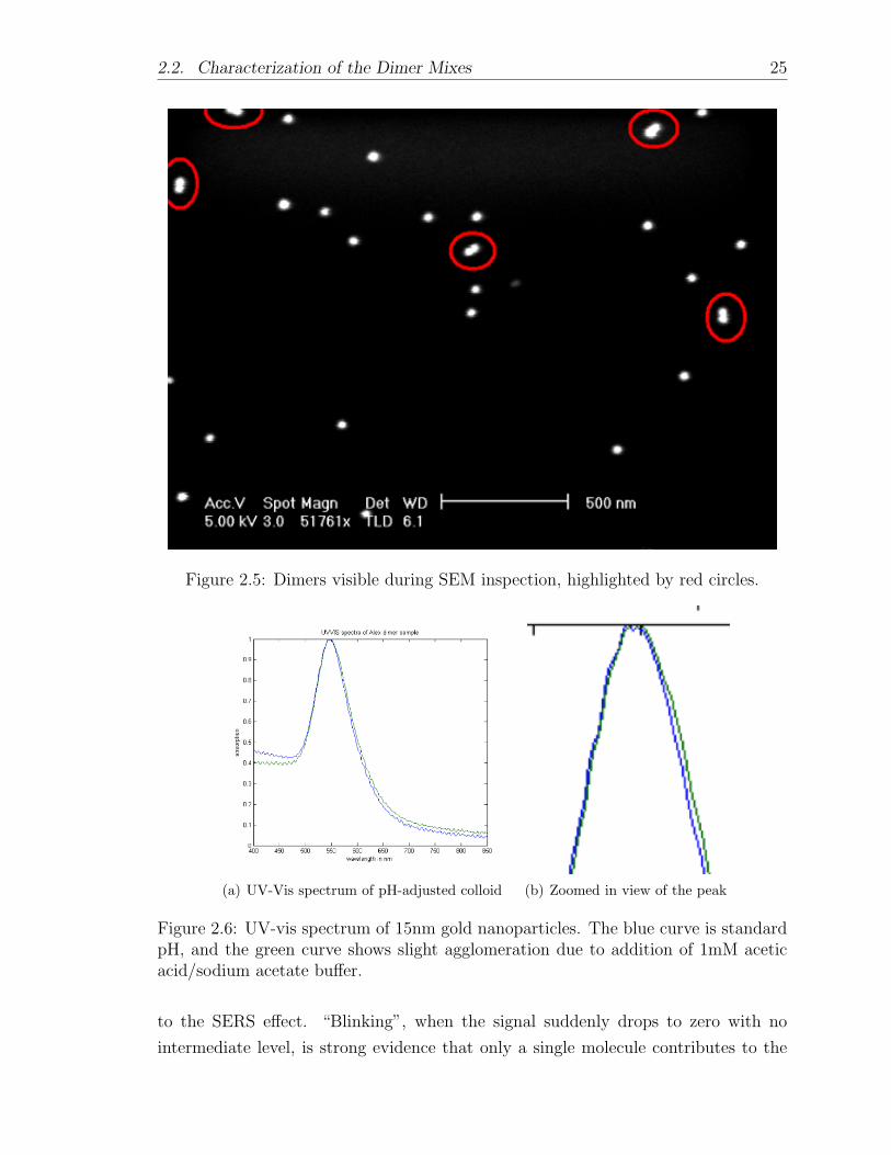
Figure 2.5: Dimers visible during SEM inspection, highlighted by red circles.
(a) UV-Vis spectrum of pH-adjusted colloid (b) Zoomed in view of the peak
Figure 2.6: UV-vis spectrum of 15nm gold nanoparticles. The blue curve is standardpH, and the green curve shows slight agglomeration due to addition of 1mM aceticacid/sodium acetate buffer.
to the SERS effect. “Blinking”, when the signal suddenly drops to zero with no
intermediate level, is strong evidence that only a single molecule contributes to the

2.3. Tweaking the Recipe 26
(a) Color of gold colloid determined by particlesize. Image from commercial supplier.
(negatively charged), in which case the nanoparticles areseparated by like-charge repulsion. The steric shielding is achieved by a monolayer of TA capping agent preventingirreversible gold-gold metal bonds from forming. The smallthickness of the capping monolayer allows the particles to getclose enough together to undergo a blue colour change, whilstbeing sterically shielded from irreversible aggregation. Theresults of a series of pH changes are seen in Figure 3. Here thenanoparticle solution is changed to an acidic pH through theaddition of HCl, and then subsequently modified to a basic pHthrough the further addition of NaOH.
Figure 3. Digital photo showing the colour of the TA-capped nanoparticlesunder different pH conditions, where a) the sample is at its initial pH of 5.84,
b) the addition of 50 l of HCl (1 M) modifies the pH to 2.49, and c) the addition of 50 l of HCl (1 M) caused a blue colour change which was
subsequently followed by the addition of 100 l of NaOH (1 M) resulting in a final pH of 11.34 and a recovery of the red solution colour.
That the particles are capable of being resuspended isevidence that the TA capping agent sterically shields thenanoparticles from irreversible gold-gold metallic bindingwhen the electrostatic stabilization is removed at the acidicsolution pH, (i.e. the protonation of the carboxylic acid end-groups resulting in a decrease of the surface charge on thenanoparticles).
C. TEG-capped nanoparticlesThe ability of TEG to minimize non-specific binding is
seen in Figure 4, where the particles which are capped with TEG exhibit a minimal shift in their absorption spectrum whenAvidin is added to the system. The non-specific binding ofAvidin to citrate-stabilized nanoparticles is demonstrated bythe red-shift of the absorption peak for unprotectednanoparticles under the same addition of Avidin.
400 500 600 700 800
0.0
0.2
0.4
0.6
0.8
1.0
Abso
rptio
n
Wavelength (nm)
Citrate-stabilizedCitrate + Avidin TEG-capped TEG + Avidin
Figure 4. Visible absorption spectra of 1 ml of citrate-stabilized, and TEG-capped, nanoparticles before and 10 minutes after the addition of 10 l of
Avidin (200 g/ml).
D. NTA and mixed NTA/TEG cappingThe absorption spectra for citrate, TEG- and NTA-
stabilized nanoparticles are seen in Figure 5. The plasmonabsorption peaks are shown in Table 1 for both theexperimental data and for theoretical calculations using thetheory described by Mulvaney [5].
400 500 600 700
0.0
0.2
0.4
0.6
0.8
1.0
Abso
rptio
n
Wavelength (nm)
Citrate-stabilized TEG-capped NTA-capped
Figure 5. Visible absorption spectra of citrate-stabilized, TEG-capped, and NTA-capped nanoparticles which indicate respective plasmon absorption
peaks at 518.2, 521.5, and 524.9 nm.
TABLE I. THEORETICAL AND EXPERIMENTAL PLASMON PEAKPOSITIONS FOR CAPPED NANOPARTICLES.
Plasmon Absorption Peak position and Shift (nm)Cappingagent Theoretical Shift Experimental Shift
Citrate 519.3 - 518.2 -
TEG 521.2 1.9 521.5 3.3
NTA 521.8 2.5 524.5 6.3
As can be seen from Table 1, the nanoparticles display an experimental peak-absorption shift about twice that predictedby the theory [5]. However, the data qualitatively agrees withthe theoretical model, as the longer NTA capping agent showsa greater shift compared to that of the shorter TEG cappingagent.
The relative concentration of NTA and TEG compounds onthe surface of the nanoparticles is expected to be proportional to their concentration in solution. The Zeta potentials of thevarious mixed NTA/TEG-capped nanoparticle samples areseen in Figure 6. The Zeta potential provides an indication ofthe amount of charge on the surface of the nanoparticles;however, both the ionic strength and the pH of the solution are important factors during Zeta potential measurements.
In general, there is a trend indicating that larger relativeamounts of NTA in solution lead to larger Zeta potentials forthe incubated nanoparticles. Sample 1, which is capped withonly TEG molecules, shows a potential of -12 mV. Sample 9, which is NTA-capped, shows a potential of -30 mV. Samples2-8 show the trend of increasing Zeta potential with increasingratio of NTA to TEG in solution during incubation.
222
(b) Apparent agglomer-ation of colloid followingacidification, reversed byincreasing pH. From (30).
Figure 2.7: Colors of gold colloid. (a) The color transitions from a deep red to apeachy orange for large diameter particles. (b) Agglomeration of 15nm colloid underacidification. Original color shown in (A) and recovered in (C). The agglomeration(visible in (B)) was reversible in this case due to the presence of a protecting mono-layer. See (30). Citrate-stabilized colloid permanently agglomerates under acidicconditions.
observed signal. The signal blinks off when the molecule no longer responds to the
incident light, usually as a result of damage to its structure.
On a few occasions, we observed a Raman signal in a dimer mix, seeming to
indicate that the dimers were bound by the linker molecule. However, we were unable
to replicate these results in numerous repeated efforts. Additionally, we observed no
discernible difference between control mixes and varied linker concentrations during
SEM inspection. This led us to believe that in fact no linking was taking place. The
apparent Raman signal seen on several occasions remains mysterious, but most likely
it resulted from some human error, either inadvertent contamination of the sample or
addition of the molecule in a concentration several orders of magnitude higher than
intended. The latter mistake would actually be fairly easy to make. During serial
dilution, if one was to skip the final dilution step, transfer from the wrong solution, or
miscalculate the amount to transfer in each step, the final concentration could vary
drastically from the expected value.
2.3 Tweaking the Recipe
We came up with several explanations for why the dimer recipe failed to actually
produce dimers joined by single molecules. One hypothesis was that disulfide forma-
tion between the thiol end groups was polymerizing the linker molecules. Though
we were already using a protected thiol, and only performing the deprotection step

2.3. Tweaking the Recipe 27
Figure 2.8: Apparent Raman enhancement within a dimer of 250nm nanoparticles.However, results such as these were not reproducible. Inset: SEM image of the dimersupposedly responsible for signal.
in a nitrogen environment, trace amounts of oxygen could have oxidized the thiols
to disulfides. To combat the oxidation of the thiols, we added an excess of sodium
borohydride (NaBH4), a strong reducing agent. NaBH4 is known to reduce disulfide
bonds to free thiols; it is commonly used as a protein denaturant. However, the
addition of reducing agent did not result in apparent linking (see Table 2.1).
Another hypothesis was that the formation of the Au-S bond requires the presence
of an oxidizing agent, and mixing the reagents under nitrogen was actually inhibiting
the linking process. Thus, we stirred the mix in open air and bubbled air through
the mix to ensure the presence of oxygen, but we observed no linking (see Table 2.1).
We also considered the possibility that the linker molecule is out-competed by
the citrate ions for access to the gold surface. Because it is stabilized by citrate, the
conjugate base of a weak acid, the colloid is extremely sensitive to changes in pH.
Adding strong acid or base, even in small amounts, will cause rapid agglomeration
of the colloid. By making very slight adjustments, one can presumably “dial down”
the citrate affinity for the gold surface, opening up small gaps for the linker molecule.
Using an acetic acid/sodium acetate buffer, we gently lowered the mix’s pH until we
observed a discernible difference between a control sample and one with a large excess
of linker molecule, as determined by UV-vis spectroscopy. Unfortunately, the control

2.4. Possible Modes of Failure 28
sample turned out to have ∼5% dimers due to random agglomeration, rendering this
method infeasible for the production of single-molecule dimers.
2.4 Possible Modes of Failure
Geometry of the Au-S bond It could be that the problem is one of geometry.
Though we idealize the nanoparticles as perfect spheres, in reality their surfaces can be
quite irregular, especially at the length scale of a nanometer, the approximate length
of the BPD molecule. It could be that the molecule tends not to bind perpendicular
to the surface, as would be ideal for linking. In 2007, Jadzinsky et al. published
a high-resolution structure of a gold nanoparticle, less than a nanometer in size,
functionalized with p-mercaptobenzoic acid (p-MBA). The imaging was done by x-
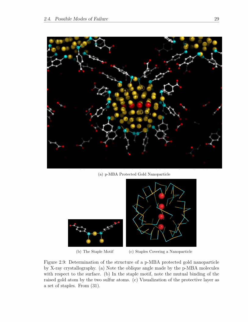
ray crystallography (31) (see Figure 2.9). They observed that the molecule tended
to bind to the surface in what they called a “staple motif” involving two sulfur
atoms and three gold atoms. These findings have important implications for our
work. Namely, the observed oblique binding angle between the p-MBA molecule
and the gold surface indicates that our linker molecule may need to be longer in
order to effectively stretch between two nanoparticles. Alternatively, we could use a
linker molecule with methylene groups on the end to provide flexibility; however, this
change would suppress conductance. The observation of the staple motif also suggests
cooperativity between pairs of Au-S bonds; perhaps a single Au-S bond is unstable.
This hypothesis would explain why monolayers form readily on nanoparticle surfaces,
yet single-molecule linking has proved so challenging. The authors also noted stacking
of the p-MBA phenyl rings, another point favoring monolayer formation over binding
of a single molecule. The evidence noted here suggests a “heterogeneous monolayer”
approach might have more success, where a linker molecule is embedded within a
monolayer formed by a stub thiol. The diluent thiol could presumably stabilize the
Au-S bond of the linker and favorably interact with its hydrophobic phenyl groups.
This configuration is essentially the goal of the “click chemistry” approach discussed
later (see Chapter 3).
Kinetics The linking may also be significantly hindered by the kinetics of the sys-
tem. The linking process requires three objects to join together in a specific orienta-
tion; each is in very low concentration, and the two nanoparticles are quite massive
and thus slow-moving. On the other hand, the assembly can take place in steps,
where the linker first binds to one nanoparticle. The linking is then completed when
2.4. Possible Modes of Failure 29
Fig. S9. !"#$%&'%()#%*+,-(./%-(+0*(0+#%-)&$"12%"1(#+3.+("*/#%"1(#+.*("&1%4#5".(#5%()+&02)%
),5+&2#1%6&15"12%6#($##1%*.+6&7,/"*%.*"5-8
(a) p-MBA Protected Gold Nanoparticle
(b) The Staple Motif (c) Staples Covering a Nanoparticle
Figure 2.9: Determination of the structure of a p-MBA protected gold nanoparticleby X-ray crystallography. (a) Note the oblique angle made by the p-MBA moleculeswith respect to the surface. (b) In the staple motif, note the mutual binding of theraised gold atom by the two sulfur atoms. (c) Visualization of the protective layer asa set of staples. From (31).

2.5. Gold Colloid in Organic Solvent: Synthesis vs. Phase Transfer 30
another nanoparticle comes close enough for the free thiol to bind its surface. Also,
the frequency of nanoparticle-nanoparticle collisions must be quite high, given the
speed with which the colloid can crash out under adverse conditions. Nevertheless,
we tried to address these kinetic issues by allowing the mix to stir longer (24 hrs) at
room temperature, as well as maintaining constant stirring after transferring the mix
to the refrigerator.
Solvent Environment Another possible issue is the solubility of the linker molecule
in the predominately aqueous environment. At such low concentrations, while the
molecule may be apparently soluble, it could preferentially partition to the surface
phase of the mix, as opposed to the bulk solution phase. Returning again to the cit-
rate stabilizer, it might be that the strongly charged environment of the nanoparticle
surface is energetically unfavorable for the molecule. Whatever the exact cause, we
investigated the possibility of performing the linking reaction in an all-organic solvent
environment more favorable to linker molecule solubility.
2.5 Gold Colloid in Organic Solvent: Synthesis vs.
Phase Transfer
Numerous recipes have been reported for the synthesis of gold colloid dispersible in
organic solvent, representing variations on a recipe developed by Brust et al. in 1994
(32). In this scheme, the gold ions are transferred from the aqueous phase into the
organic phase by means of a phase-transfer catalyst. The reduction and particle
nucleation then takes place in the organic phase. Particle growth halts when the
passivating molecule, an alkanethiol, can completely cover the surface area of the
nanoparticles. It is easy to imagine how one could make dimers by this method,
introducing a small amount of dithiol complemented by alkanethiol in much greater
concentration, thereby synthesizing both the nanoparticles and the dimers in one fell
swoop. However, we found it difficult to synthesize monodisperse, regularly shaped
colloid with diameters greater than roughly 40nm or so, while our contacting method
is ideally suited to larger nanoparticles (diameter >100nm).
These larger nanoparticles are commercially available and are generally monodis-
perse and regular. However, the commercial gold colloid is only available in aque-
ous solvent. We briefly explored phase-transfer methods as an alternative to direct
synthesis in organic solvent, hoping to combine the convenience and regularity of

2.6. Alternate Ligands 31
commercial colloid with the potentially favorable properties of the organic environ-
ment. Several techniques have been reported in the literature for phase transferring
gold nanoparticles into nonpolar organic solvent. One method developed by Lala et
al. rendered octadecanethiol molecule water-soluble by forming inclusion complexes
with cyclodextrin. The water-soluble thiol was then introduced to the nanoparticles,
and during vigorous shaking of a biphasic mixture, the gold colloid migrated to the
organic phase (33). We followed their recipe and found some success when using thi-
ols with shorter alkyl chains (up to 8 carbons). One of the major drawbacks of this
approach, and similarly with the direct synthesis method, is that the linker molecule
now must displace covalently bound thiols, as opposed to weakly adsorbed citrate
ions, in order to link two nanoparticles.
We considered replacing the stabilizing layer with alkyl amines to facilitate inclu-
sion of the linker into the SAM on the nanoparticle surface. Given the relatively weak
coupling between nitrogen and gold atoms, we believed that the linker dithiol could
replace the amines and bind to the nanoparticles. Sastry et al. reported a protocol
for the phase transfer of gold nanoparticles into toluene using octadecylamine (ODA)
as the transfer agent (34). However, we were unable to replicate their results despite
several attempts, using nonylamine and dodecylamine instead of ODA. We attempted
a similar protocol using several other agents—benzonitrile, benzyl mercaptan, dode-
canethiol, and 4-butylaniline—though none proved effective at phase transferring the
colloid.
2.6 Alternate Ligands
In light of the results of Venkataraman et al. (see 1.1.2), and those of Jadzinsky
et al. (see 2.4), we explored the use of diamines as an alternative to dithiol linker
molecules. Though the gold-nitrogen (Au-N) bond is much weaker than the Au-S
bond, it appears to preferentially form such that the molecule sits perpendicular to
the surface (12). This property would certainly facilitate linking. Using a similar
recipe to the standard approach developed for the dithiol molecule, we attempted to
form dimers by addition of o-tolidine, a diamine analogous to BPD except for the
presence of two methyl groups. As with the dithiol, however, the control sample was
not markedly different from one containing the molecule. Consequently, the further
use of diamines was put on hold to focus efforts on other approaches.
Bipyridine molecules could represent another substitute for dithiols. Bipyridine
has been used occasionally in mechanical break junction measurements with STM,
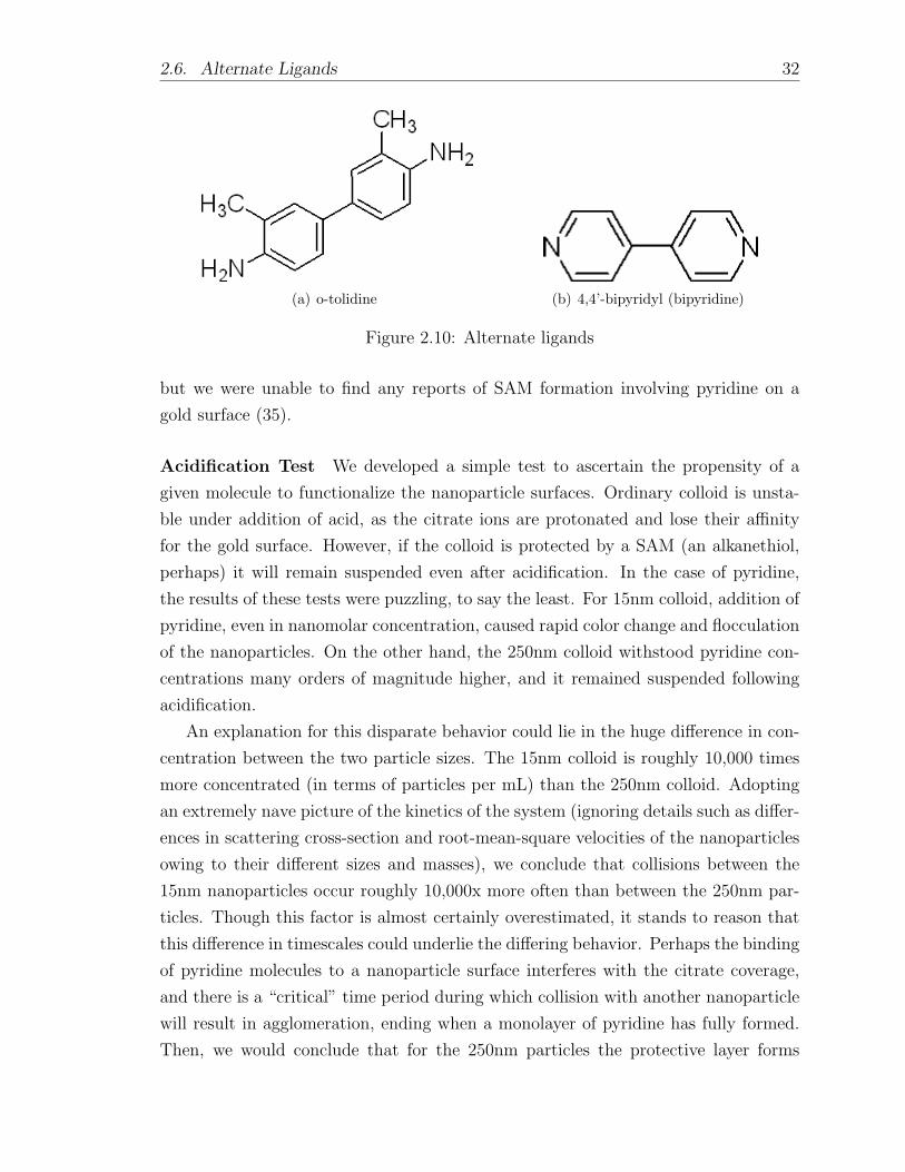
2.6. Alternate Ligands 32
(a) o-tolidine (b) 4,4’-bipyridyl (bipyridine)
Figure 2.10: Alternate ligands
but we were unable to find any reports of SAM formation involving pyridine on a
gold surface (35).
Acidification Test We developed a simple test to ascertain the propensity of a
given molecule to functionalize the nanoparticle surfaces. Ordinary colloid is unsta-
ble under addition of acid, as the citrate ions are protonated and lose their affinity
for the gold surface. However, if the colloid is protected by a SAM (an alkanethiol,
perhaps) it will remain suspended even after acidification. In the case of pyridine,
the results of these tests were puzzling, to say the least. For 15nm colloid, addition of
pyridine, even in nanomolar concentration, caused rapid color change and flocculation
of the nanoparticles. On the other hand, the 250nm colloid withstood pyridine con-
centrations many orders of magnitude higher, and it remained suspended following
acidification.
An explanation for this disparate behavior could lie in the huge difference in con-
centration between the two particle sizes. The 15nm colloid is roughly 10,000 times
more concentrated (in terms of particles per mL) than the 250nm colloid. Adopting
an extremely nave picture of the kinetics of the system (ignoring details such as differ-
ences in scattering cross-section and root-mean-square velocities of the nanoparticles
owing to their different sizes and masses), we conclude that collisions between the
15nm nanoparticles occur roughly 10,000x more often than between the 250nm par-
ticles. Though this factor is almost certainly overestimated, it stands to reason that
this difference in timescales could underlie the differing behavior. Perhaps the binding
of pyridine molecules to a nanoparticle surface interferes with the citrate coverage,
and there is a “critical” time period during which collision with another nanoparticle
will result in agglomeration, ending when a monolayer of pyridine has fully formed.
Then, we would conclude that for the 250nm particles the protective layer forms

2.6. Alternate Ligands 33
quickly enough that the probability of agglomeration is very low, and not fast enough
to prevent agglomeration for the 15nm particles. If this theory is indeed correct, then
following sufficient dilution the 15nm colloid should survive the addition of pyridine;
likewise, sufficiently concentrated 250nm particles should agglomerate when pyridine
is added. However, the factors by which the colloid must be concentrated/diluted to
observe these effects are likely quite impractical. Nevertheless, the results with the
250nm colloid suggest that bipyridine may indeed be a viable linker molecule, and it
merits further investigation.

Chapter 3
The “Click” Approach
Finally, we sought to make dimers by “click” chemistry rather than direct introduc-
tion of a linker molecule. In this approach, the nanoparticles are functionalized with
precursors that will be joined together by chemical reaction. The reaction is formally
known as Copper(I)-catalyzed Azide-Alkyne Cycloaddition (CuAAC), forming a tria-
zole ring. This reaction is handy for several reasons: it works best in aqueous solvent;
it is extremely high-yield; and it works well despite low concentrations of reactants.
Joining nanoparticles by this reaction has been previously demonstrated; however, in
that work the goal was not to make single-molecule junctions, nor were the molecules
particularly interesting candidates for conductance measurements (36). This reaction
has also been used to join a molecule to a relatively high-conductance ligand bound
to a gold surface, demonstrating its usefulness in the context of electron transport
measurements (37).
We have developed the following scheme to make use of the CuAAC reaction.
First, the nanoparticles are functionalized with a mix of stub thiols and azide-terminated
thiols. When present in suitably low concentration with respect to the stub thiol, each
nanoparticle should only have one azide, permitting the formation of dimers but ren-
dering formation of higher-order structures impossible. Following introduction of a
diacetylene linker and catalyst, the “click” reaction should proceed to join pairs of
nanoparticles. One of the nice features of this reaction is that its yield theoretically
could be 100%, unlike dithiol linking which is effectively capped at ∼10% if one wishes
to stay in the single-molecule regime. Also, with some clever chemistry this method
could be applied to make trimers or even more complex structures, though certainly
that goal is well beyond our current capabilities.

3.1. Resin Approach: Single-Molecule Functionalization 35
3.1 Resin Approach: Single-Molecule Functional-
ization
We originally tried a resin-based synthesis as a means of functionalizing the nanopar-
ticle with a single azide.1 The nanoparticles were to be passivated with a monolayer
capped with diazonium groups. The nanoparticle can then bind to a benzylamine
resin. Because of the spacing of the active sites in the resin, the nanoparticle would
be bound by exactly one molecule. During the cleave step, this molecule would be
converted to an azide, and thus each nanoparticle would be monofunctionalized with
azide. See Figure 3.1 below. In practice, however, we found that the nanoparticles
were too big to effectively penetrate the pores of the resin. We abandoned the resin-
based approach in favor of the less elegant, but hopefully more effective, monolayer
method.
Figure 3.1: An overview of the steps in the resin-based “click” synthesis
1Resin-based approach proposed by Wataru Ebina.

3.2. Functionalization/Characterization of the Nanoparticles with HeterogeneousMonolayers 36
3.2 Functionalization/Characterization of the Nanopar-
ticles with Heterogeneous Monolayers
As discussed in earlier sections, the ideal solvent environment for the nanoparticles—
pure water—will poorly solubilize organic molecules with long alkyl chains. Here, we
report the use of an anionic surfactant to render alkanethiols soluble in the aqueous
medium of the gold colloid. Thus, we can functionalize the gold nanoparticles using
a minimal amount of organic solvent. We use sodium dodecyl sulfate (SDS) as the
surfactant, which is readily water soluble with a critical micelle concentration (CMC)
of ∼8mM. As an additional bonus, SDS is also known to effectively stabilize gold
colloid. When dissolved in ethanol and introduced slowly, the alkanethiol is incorpo-
rated into the micelles formed by the surfactant, thereby providing “reservoirs”, so
to speak, of thiol to bind the gold surfaces of the nanoparticles.
The nanoparticles can then be characterized by several techniques. First, one can
acidify the colloid; if it agglomerates, then it is likely that the monolayer failed to form
(see 2.6). The nanoparticles are first centrifuged and re-suspended multiple times in
pure water to remove excess thiol and SDS. As a control, we acidified colloid that
originally contained only SDS and observed that it agglomerated. The alkanethiol-
capped nanoparticles, on the other hand, survived acidification, indicating that a
monolayer had indeed coated the gold surface.
Additionally, they can be characterized by X-ray photoelectron spectroscopy (XPS),
a spectroscopy method that performs elemental analysis by determining the kinetic
energy of electrons ejected from the surface of a sample. Another technique that may
prove useful is infrared (IR) spectroscopy, which excites vibrational modes of the
bonds between atoms and can be used to identify the presence of certain functional
groups.
We are currently working to extend this surfactant-based method to azide-terminated
thiols. Initial attempts appear to have failed, based on XPS data as well as the qual-
itative acidification test. These failures are likely related to the age of the thioazide
we were using; perhaps the free thiol has oxidized over time and is now inactive. We
have just received a fresh batch and will be retrying this method. The end goal will
be to functionalize a nanoparticle with a fully conjugated molecule terminated by
thiol and azide groups in order to maximize conductance, with a diluent alkyl thiol
to make up the rest of the monolayer.
3.3. Clicking the Nanoparticles Together 37
3.3 Clicking the Nanoparticles Together
Once we have successfully functionalized the nanoparticles with azide, the next step
will be to perform the CuAAC reaction to make dimers. The “click” reaction is
performed in the presence of copper(I) ions, which serve as a catalyst. Cu1+ ions
are unstable in aqueous solution, so this catalyst is typically made in situ by reduc-
tion of copper(II), and stabilized by tris[(1-benzyl-1H-1,2,3-triazol-4-yl)methyl]amine
(TBTA). Based on the concern that the reduction of copper ions might plate metal
onto the nanoparticles, we add Cu metal, instead of a strong reducing agent, to the re-
action mix containing Cu2+. Phenyl diacetylene, a molecule terminated by two alkyne
groups, serves as the linker to join two azide-terminated molecules. See appendix for
a detailed reaction procedure.
Following the synthesis step, the nanoparticles can be characterized by SEM in-
spection. IR spectroscopy could also provide evidence of the triazole ring, the product
of the click reaction.

Future Directions
Currently, the most promising approach to dimer synthesis appears to be the “click”
method, making use of the CuAAC reaction. No doubt, certain aspects of the di-
rect approach deserve to be revisited, such as the investigation of alternate ligands
and possible methods of stabilizing the Au-S bond. The CuAAC reaction, on the
other hand, has proved to be exceptionally robust, and it has been used to produce
structures similar to the single-molecule dimers we hope to make.
Once we can successfully make dimers that unambiguously contain single molecules,
we can revisit the contacting technique and hopefully measure electron transport
through the bound molecule. In the following section, I have laid out a few of the
problems we expect might arise when patterning contacts to the molecule, along with
potential solutions.
4.1 Will Processing Damage the Molecule?
One major doubt is that the molecule might become unbound when applying resist.
The resist deposition process involves a bake step to remove solvent and harden the
plastic. Typical recipes using poly(methyl methacrylate) (PMMA) bake at 180C for
2 minutes. Such high temperature could potentially cause irreparable harm to the
molecule. One concern is the possible dissociation of the Au-S bond. Thermogravi-
metric analysis (TGA), where the relative weight loss of a nanoparticle is measured
with increasing temperature, demonstrates that passivating thiol layers on gold typ-
ically begin to vaporize at temperatures ca. 200C (38). While this is no guarantee
that the molecule will emerge unscathed from a bake step at 180C , it is at least
somewhat reassuring. That being said, we can reduce the temperature of this bake
step if necessary. The high temperature serves mostly to quickly drive off the solvent.
At lower temperatures, baking in a vacuum oven can expedite the solvent evapora-
tion. PMMA undergoes a glass transition around 105C. We have experienced some
difficulties baking below this temperature when depositing a thick layer (>50nm) of

4.1. Will Processing Damage the Molecule? 39
thermally evaporated metal (see Figure 4.2) despite a slow evaporation rate.
Figure 4.2: SEM image of a device after PMMA outgassed during metal evaporation,possibly due to insufficient baking.
A final concern is if the e-beam lithography itself might damage the molecule,
as high-energy electrons are scattered mere tens of nanometers away. Given the
molecule’s small cross-section, as well as the shield provided by the nanoparticle and
thick layer of resist, stray electrons might not pose a threat. However, if this issue
arises, it could be addressed by using larger nanoparticles, thereby putting greater
distance between the patterned area and the molecule.
4.1.1 Metallized DNA
Another promising area to investigate is the use of metallized DNA to bind to the
ends of a molecule. However, many problems remain to be solved before metallized
DNA can be used as a reliable electrical contact to single molecules. As noted earlier,
grain formation in the metal coating on the DNA results in poorly conducting wires.
Probably the biggest question mark is the quality of the contact between the DNA
and the target molecule. In 2003, Keren et al. reported the fabrication of a field-
effect transistor based on a single-walled carbon nanotube (SWNT) contacted by
metallized DNA (39). They noted the presence of a large series resistance in the

4.1. Will Processing Damage the Molecule? 40
device, which they attributed to poor contact between the SWNT and DNA (see
Figure 4.3). In order to effectively measure electron transport, the contact between
DNA and molecule will need to be well characterized and likely significantly improved.
Figure 4.3: Carbon nanotubes contacted by metallized DNA. Note the grains in the“wire.” (a) A single SWNT. (b) A rope of SWNTs. Scale bars 100nm. From (39).

Appendix A
Experimental Methods
Chemicals and Glassware All chemicals were used as received from the manufac-
turer with no additional purification. The gold colloid was purchased from Ted Pella,
Inc. Some processes had dedicated glassware; otherwise, disposable 20mL scintillation
vials were used for most experiments.
A.1 Gold Colloid in Organic Solvent
A.1.1 Synthesis
Gold colloid in toluene was synthesized following an adaptation of the recipe published
by Brust et al. (32). The following is a typical recipe used to make small (diameter
∼5nm) nanoparticles. 17.75 mg of HAuCl4 was dissolved in 6mL of deionized water.
4.0mg of tetraoctylammonium bromide (TOAB) was dissolved in 16mL of toluene.
The water and toluene were then mixed, and after stirring for about 20 minutes,
the orange color had migrated from the aqueous to the organic phase. 34mg of
dodecanethiol was added to the organic phase. Then, a freshly-prepared solution
containing 18.9 mg sodium borohydride (NaBH4) in 5mL deionized water was added
slowly to the stirring solution. The mix was then allowed to stir overnight. The
following day, the organic phase was washed once with dilute H2SO4 and twice with
pure deionized water.
A.1.2 Phase Transfer
α-cyclodextrin inclusion complexes Following the method of (33), 100mg of
α-cyclodextrin was dissolved in 5mL of distilled water and warmed gently to a tem-

A.2. Dimer Mixes 42
perature of 50C. Then, 1.8µL of octanethiol was added. The mix was allowed to
stir for 2 days at 50C, after which time the octanethiol had apparently dissolved.
Then, 1mL of 80nm gold colloid was added, along with 5mL of chloroform. During
sonication, the reddish color migrated from the aqueous phase to the organic.
Phase transfer by fatty amines This procedure was adapted from the method
reported by Sastry et al. (34). A solution containing 20µL of nonylamine in 1ml
toluene was prepared. 1mL of 80nm colloid was then added, but no phase transfer
was observed despite vigorous shaking and sonication.
A.2 Dimer Mixes
A.2.1 Preparation
The following is a typical example of a dimer mix, prepared so as to have a 1:10
ratio of linker molecule to nanoparticles. The 250nm colloid contains 3.6×10⁻⁸ parti-
cles/mL. To 1mL of colloid, we added 10µL of NH4OH to cleave the protecting groups
from the linker molecule. The mix was then transferred to a glove bag filled with ni-
trogen, and we then added 0.5mL of 4,4’-biphenyl dithioacetate (BPDAc) dissolved
in 3:2 tetrahydrofuran (THF) / ethanol (EtOH), containing 3.6×10⁻⁷ molecules of
linker. This dilute solution was prepared by dissolving 2mg of BPDAc in 5 mL
of 3:2 THF/EtOH, then serially diluting by transferring 40.8µ into another 5mL of
THF/EtOH a total of 5 times. The mix was then allowed to stir for about 4 hours
before being sealed with parafilm, removed from the glove bag, and stored in the
refrigerator at 4C.
A.2.2 Deposition Process
We deposited gold nanostructures onto silicon (Si) wafers using the following tech-
nique. The wafer was placed under an ozone lamp for 10 minutes, then cleaned
with acetone, isopropyl alchol (IPA), and Milli-Q water to remove surface contami-
nants. 25µL of poly-L-lysine was deposited on the surface, and the wafer was spun
at 3000rpm to ensure even coverage. This step provides an adhesive layer to bind
the nanoparticles. Then, 50µL of the colloid or dimer mix was deposited on the sur-
face and spun at 4000rpm. For the more dilute mixes (i.e. those containing larger
nanoparticles), this deposition step was repeated 2-3 times.

A.3. Fabrication of Contacts 43
A.3 Fabrication of Contacts
An alignment grid with markers spaced by 20µ was patterned onto the Si wafer
using standard lithography techniques. Then, the nanoparticles are deposited on
the surface as described above. Suitable candidates for contacting are located in
an optical microscope under dark field imaging, which makes the nanoparticles very
visible. A digital camera attached to the microscope captures an image of the particle
and the adjacent grid marks. This image file is then processed to make an alignment
file to direct the SEM. The wafer is covered with a thick layer (roughly a micron) of
PMMA in multiple deposition steps. Each step is followed by baking in a vacuum
oven to remove the solvent. Large bond pads are patterned close to the nanoparticles
of interest and 30nm of Ti/Au is deposited. The PMMA deposition is repeated, and
the alignment file is used to pattern contacts stretching between the bond pads and
the nanoparticles. A thick layer (roughly 200nm) of Au is then deposited by thermal
evaporation, since we found that for some reason, electron-beam evaporated gold
would not stick to the nanoparticles. During liftoff, the wafer is minimally sonicated
to remove excess gold without dislodging the nanoparticles.
A.4 The “Click” Process
The following is a typical procedure for attempting to “click” the nanoparticles. Since
there is no diluent thiol, the resulting junction will not be single-molecule.
A.4.1 Functionalization of the Nanoparticles
We prepared 5mL of a 20mM solution of sodium dodecyl sulfate (SDS) in distilled
water. To this solution, we added 1mL of 15nm colloid. While rapidly stirring, we
then added 50µL of a solution containing 2mg of azido-undecanethiol in 5mL ethanol.
Excess azide was then removed by repeatedly centrifuging out the nanoparticles, re-
placing the supernatant with pure distilled water, and redispersing the nanoparticles.
A.4.2 Performing the “Click” Reaction
The nanoparticles are separated into two populations. To 1mL of nanoparticles, we
add an excess of phenyl diacetylene, along with 10µL of 50mM aqueous Cu(NO3)2,
30mM of TBTA in dimethyl sulfoxide (DMSO), and a small piece of copper metal
that has been polished with sandpaper to remove any oxide.

References
[1] A. Neuhausen, Private communication, 2008.
[2] A. Aviram and M. A. Ratner, Chemical Physics Letters 29, 277 (1974).
[3] Y. Xue and M. A. Ratner, Physical Review B 68 (2003).
[4] Online at: http://www.ehcc.kyoto-u.ac.jp/laboratory/material/material.htm,
2008.
[5] H. C. Kolb, M. G. Finn, and K. B. Sharpless, Angewandte Chemie International
Edition 40, 2004 (2001).
[6] A. Nitzan and M. A. Ratner, Science 300, 1384 (2003).
[7] K. I. Bolotin, F. Kuemmeth, A. N. Pasupathy, and D. C. Ralph, Applied Physics
Letters 84, 3154 (2004).
[8] L. A. Bumm et al., Science 271, 1705 (1996).
[9] X. D. Cui et al., Science 294, 571 (2001).
[10] L. Venkataraman, J. E. Klare, C. Nuckolls, M. S. Hybertsen, and M. L. Steiger-
wald, Nature 442, 904 (2006).
[11] N. Agraıt, J. G. Rodrigo, and S. Vieira, Physical Review B 47 (1993).
[12] L. Venkataraman et al., Nano Letters 6, 458 (2006).
[13] M. A. Reed, C. Zhou, C. J. Muller, T. P. Burgin, and J. M. Tour, Science 278,
252 (1997).
[14] J. van Ruitenbeek, E. Scheer, and H. Weber, Contacting individual molecules
using mechanically controllable break junctions, in Introducing Molecular Elec-
tronics, , Springer Lecture Notes in Physics Vol. 680, pp. 253–274, Springer,
2005.

References 45
[15] H. Park, A. K. L. Lim, A. P. Alivisatos, J. Park, and P. L. McEuen, Applied
Physics Letters 75, 301 (1999).
[16] J. Park et al., Nature 417, 722 (2002).
[17] L. H. Yu and D. Natelson, Nano Letters 4, 79 (2004).
[18] A. A. Houck, J. Labaziewicz, E. K. Chan, J. A. Folk, and I. L. Chuang, Nano
Letters 5, 1685 (2005).
[19] Z. K. Keane, J. W. Ciszek, J. M. Tour, and D. Natelson, Nano Letters 6, 1518
(2006).
[20] D. R. Ward et al., Nano Letters 8, 919 (2008).
[21] D. P. Long et al., Applied Physics Letters 86, 153105 (2005).
[22] T. Dadosh et al., Nature 436, 677 (2005).
[23] C. Zhou, M. R. Deshpande, M. A. Reed, L. Jones II, and J. M. Tour, Applied
Physics Letters 71, 611 (1997).
[24] C. P. Collier et al., Science 289, 1172 (2000).
[25] C. P. Collier et al., Science 285, 391 (1999).
[26] R. F. Service, Science 302, 556 (2003).
[27] C. N. Lau, D. R. Stewart, R. S. Williams, and M. Bockrath, Nano Letters 4,
569 (2004).
[28] J. E. Green et al., Nature 445, 414 (2007).
[29] L. C. Brousseau, III, J. P. Novak, S. M. Marinakos, and D. L. Feldheim, Ad-
vanced Materials 11, 447 (1999).
[30] C. S. Barton et al., Functional monolayer surfaces on gold nanoparticles for
specific binding of histidine-tagged proteins, in Nanoscience and Nanotechnology,
2006. ICONN ’06. International Conference on, 2006.
[31] P. D. Jadzinsky, G. Calero, C. J. Ackerson, D. A. Bushnell, and R. D. Kornberg,
Science 318, 430 (2007).

References 46
[32] M. Brust, M. Walker, D. Bethell, D. J. Schiffrin, and R. Whyman, Journal of
the Chemical Society , 801 (1994).
[33] N. Lala, S. P. Lalbegi, S. D. Adyanthaya, and M. Sastry, Langmuir 17, 3766
(2001).
[34] M. Sastry, A. Kumar, and P. Mukherjee, Colloids and Surfaces A: Physicochem-
ical and Engineering Aspects 181, 255 (2001).
[35] B. Xu and N. J. Tao, Science 301, 1221 (2003).
[36] R. Voggu, P. Suguna, S. Chandrasekaran, and C. N. R. Rao, Chemical Physics
Letters 443, 118 (2007).
[37] J. P. Collman et al., Science 315, 1565 (2007).
[38] X. Zou et al., Journal of Colloid and Interface Science 295, 401 (2006).
[39] K. Keren, R. S. Berman, E. Buchstab, U. Sivan, and E. Braun, Science 302,
1380 (2003).