metallurgy of high-silicon steel parts produced using
TRANSCRIPT

lable at ScienceDirect
Acta Materialia 110 (2016) 207e216
Contents lists avai
Acta Materialia
journal homepage: www.elsevier .com/locate/actamat
Full length article
Metallurgy of high-silicon steel parts produced using Selective LaserMelting
Michele Garibaldi, Ian Ashcroft*, Marco Simonelli, Richard HagueAdditive Manufacturing and 3D Printing Research Group, Faculty of Engineering, The University of Nottingham, Nottingham NG7 2RD, United Kingdom
a r t i c l e i n f o
Article history:Received 10 February 2016Received in revised form11 March 2016Accepted 12 March 2016Available online 22 March 2016
Keywords:Additive manufacturingFerritic steelsDirectional solidificationTextureSolidification microstructures
* Corresponding author.E-mail address: [email protected] (I.
http://dx.doi.org/10.1016/j.actamat.2016.03.0371359-6454/© 2016 The Authors. Published by Elsevierlicenses/by/4.0/).
a b s t r a c t
The metallurgy of high-silicon steel (6.9%wt.Si) processed using Selective Laser Melting (SLM) is pre-sented for the first time in this study. High-silicon steel has great potential as a soft magnetic alloy, but itsemployment has been limited due to its poor workability. The effect of SLM-processing on the metallurgyof the alloy is investigated in this work using microscopy, X-Ray Diffraction (XRD) and Electron Back-scatter Diffraction (EBSD). XRD analysis suggests that the SLM high-silicon steel is a single ferritic phase(solid solution), with no sign of phase ordering. This is expected to have beneficial effects on the materialproperties, since ordering has been shown to make silicon steels more brittle and electrically conductive.For near-fully dense samples, columnar grains with a high aspect ratio and oriented along the builddirection are found. Most importantly, a <001> fibre-texture along the build direction can be changedinto a cube-texture when the qualitative shape of the melt-pool is altered (from shallow to deep) byincreasing the energy input of the scanning laser. This feature could potentially open the path to themanufacture of three-dimensional grain-oriented high-silicon steels for electromechanical applications.© 2016 The Authors. Published by Elsevier Ltd on behalf of Acta Materialia Inc. This is an open access
article under the CC BY license (http://creativecommons.org/licenses/by/4.0/).
1. Introduction
Over the past few years, Additive Manufacturing (AM) tech-nologies have been enjoying an ever-growing success, thanks to theunrivalled design freedom they offer for the fabrication of bothplastic and metallic components [1]. In particular, Selective LaserMelting (SLM) is emerging across a broad range of sectors,including automotive, medical and aerospace, for the creation offunctional metallic parts. SLM achieves densities comparable to thebulk material by applying a high-power laser beam to a layer ofmetallic powder, according to the data contained inside the CAD fileof the part. The laser energy fully melts the powders together,consequently creating solid metal upon cooling.
The use of laser-based AM has been investigated for processing arange of metallic materials for structural applications, includingstainless and carbon steels, as well as a number of titanium, cobaltand aluminium alloys [2e5]. However, the potential of thismanufacturing technology for applications other than structural isalmost unexplored. A significant example in this regard is repre-sented by those materials with ferromagnetic properties, such as
Ashcroft).
Ltd on behalf of Acta Materialia Inc
soft and permanent magnets. Applications that rely upon suchmaterials include the large family of devices that transform elec-trical energy into mechanical energy, such as motors, and frommechanical to electrical, such as AC generators. The contribution ofZhang et al. [6] is the sole example of the application of SLM forprocessing a soft magnetic alloy. In their paper, the authors showedthe beneficial effect of microstructure refinement by SLM-processing on the DC soft magnetic properties of Permalloy. Thelack of further reference on the topic indicates a gap in the litera-ture, as it seems that the successful processing of magnetic corematerials through AM has the potential to open the path to a newgeneration of designs for highly performing electromechanicaldevices.
An important class of soft magnetic materials are silicon steels,which are iron alloys with silicon in concentrations ranging from2e7%wt. Within the family of silicon steels, Fe-6.5%Si alloys have ahigh potential in magnetic device applications due to their highelectrical resistivity, near-zero magnetostriction, and low magne-tocrystalline anisotropy [7]. Despite their high potential, these al-loys are rarely used in commercial applications because of theirvery limited ductility, which results in poor workability. A recenttechnique developed by JFE Steel employs a chemical vapourdeposition treatment to add silicon once the lamination has beencreated [8]. The two 6.5%Si lamination types obtained through this
. This is an open access article under the CC BY license (http://creativecommons.org/

M. Garibaldi et al. / Acta Materialia 110 (2016) 207e216208
technique, namely JNEX and JNHF, represent the only examples ofcommercialised high-silicon electrical steels. Other attempts ofhigh-silicon steel processing have been explored in the literature, inthe form of powder cores [9], cast strips [10] and electron-beamphysical vapour deposited sheets [11].
The tool-free nature of SLM could offer an alternativemanufacturing route for processing near-fully dense high-siliconsteel parts with unique microstructural properties. Importantly,owing to the additive nature of the SLM process and the thermalhistory the material experiences, a crystallographic texture can beinduced. A number of contributions have shown that SLM pro-cessing can create interesting crystallographic features [12,13]. InRefs. [12], a high power laser was employed to produce highlyanisotropic stainless steel with strong morphological and crystal-lographic textures. In Refs. [13], it was shown that changing thescan strategy (i.e., the path followed by the processing laser) affectsthe crystallographic texture of AlSi10 Mg. The authors showed thata strong fibre texture obtained by scanning every layer using uni-directional vectors could be changed into a weak cube texturewhen scan vectors rotated by 90� within and between layers wereemployed. As regards to the silicon steels, controlling the crystal-lographic texture is very attractive in a number of applications,since the <001> crystallographic direction is the “easy axis” ofmagnetisation [14]. While cold rolling is a widespread method toobtain laminations with strong <001> texture along the rollingdirection and <101> texture along the transverse and normal di-rections (cube-on-edge or Goss texture, as explained in Ref. [15]), amanufacturing process able to produce cube-textured parts couldpotentially extend the applicability range of the alloy.
The aim of this paper is to show that three-dimensional high-silicon steel parts can be manufactured using SLM and to presenttheir metallurgy. First, the contribution of laser energy density isstudied with the goal of promoting part densification. Then, themicrostructure is investigated in terms of solid phase formation,grain size and morphology, as well as crystallographic texture.
2. Experimental methods
2.1. Sample manufacturing and post-processing
High-silicon steel powder with approximately 6.9% wt. Si (referto Table 1 for a list of the alloying elements) was provided by LPWTechnology Ltd., Runcorn, UK. It was experimentally verified thatthe powder particles are approximately spherical in shape with asymmetrical size distribution centred at 35 mm. Particle size rangesfrom approximately 10 mme60 mm. This is in fairly good agreementwith the range declared by the supplier (15 mm-45 mm). Powderwas first dried at 60 �C for 120 min and then processed to producetest samples using a Realizer SLM-50 (Realizer GmbH, Borchen,Germany), equipped with a continuous 100 W yttrium fibre laser(YLM- 100-AC). The SLM process was conducted under an Argonatmosphere with an oxygen level below 0.4%. The platform onwhich the specimens were built was kept at 200 �C to maintain thepart at an elevated temperature so as to reduce thermal expansiongradients. Standard cubic samples of dimensions 5 � 5 � 5 mmwere produced for analysing the porosity, crack formation and the
Table 1Alloying elements concentration range of the employed high-silicon steel powdersaccording to supplier LPW Technologies Ltd.
Element
Si Mn C P O
Concentration (%wt.) 6.9 0.05 0.01 0.009 0.0065
microstructures.As regards themanufacturing process, themain SLM parameters
are defined in Fig. 1. In the present study, laser power (P), laserbeam focus position, hatch-spacing, scan distance and layer thick-ness were kept constant. The values chosen for these parametersare those recommended by the Realizer SLM-50 manufacturer forprocessing stainless steel powders. Among the alloys routinelyprocessed using the Realizer SLM-50 (which include Co-Cr,AlSi10 Mg and Ti6Al4V), the thermal and optical properties ofatomised stainless steel powder are expected to be the closest tothose of silicon steel, owing to the similar iron content in the twoalloys. The scan speed (v) was varied in order to study the effects ofthe energy input E ¼ P/v on the material properties. As regards thescan strategy, each layer was scanned once using vectors orientedalong either the X-axis (scan direction-x, SDx) or the Y-axis (scandirection-y, SDy), alternatively. This strategy is referred to as bidi-rectional X-Y in the present manuscript. Table 2 summarises theprocess parameter values used in this study. For simplicity, eachsample is identified by the values of energy input E used to build it.For instance, the sample manufactured using P ¼ 70 W andv ¼ 0.5 m/s, which corresponds to an energy input E ¼ 140 J/m isreferred to as S140.
2.2. Study of sample metallurgy
In order to investigate the porosity andmicrostructural features,themanufactured 5� 5� 5mm cubic samples were cut along threeperpendicular planes, parallel to the cube faces. The test specimenswere cross-sectioned, mounted, and polished. The relative porositywas determined from the optical micrographs of the vertical cross-sections of the samples. An Eclipse LV100ND microscope (Nikon,Tokyo, Japan) was used to obtain the micrographs. As a quantitativemeans of assessing crack formation, the cumulative crack length(c.c.l.) was used. This parameter was defined as c:c:l: ¼ 1=n
P
i
P
jlij,
where lij is the length of the jth crack on the ith polished samplesurface and n is the total number of sample surfaces considered foreach sample. To achieve repeatability, for each test sample a min-imum of four to a maximum of six cross-sectional optical micro-graphs were acquired and analysed using the open source imageprocessing software ImageJ [16].
A TM3030 scanning electron microscope (SEM) by Hitachi,Tokyo, Japan, with a 20 kV accelerating voltage and backscatteredelectron detector was used to evaluate themicrostructures. In orderto assess grain morphology and size, SEM micrographs were ac-quired from both the horizontal (top) and vertical (front and side)cross-sections of each sample. In order to visualise melt-poolboundaries, the sample surfaces were etched by exposing them toa solution of 2% Nital for 40se60s. In addition, the SEM wasequipped with an Energy Dispersive X-ray (EDX) detector that wasused to assess the distribution of the main alloying elements in thebuilt parts.
Solid phase distribution and lattice parameter were measuredby XRD using a D500 diffractometer (Siemens, Munich, Germany)with CoKa radiation. Diffraction peaks in the range 2q ¼ [25�, 90�]were considered for determining the solid phase. The acquisitionconditions were step size Dq ¼ 0.05� and step time t ¼ 8s. Back-ground removal and Ka2 radiation stripping were performedbefore peak indexing using Diffrac. EVA software (Bruker, Billerica,Massachusetts). The lattice parameter was measured from the sixthdiffraction peak (corresponding to diffraction plane family {222}) inorder to achieve high accuracy. The acquisition conditions werestep size Dq ¼ 0.02� and step time t ¼ 30 s.
For the analysis of the crystallographic texture intensity usingEBSD, a Nova 600 Nanolab Dualbeam FIB/FEG-SEM system (FEI,Hillsboro, Oregon)was employed. EBSDmaps and pole figures were
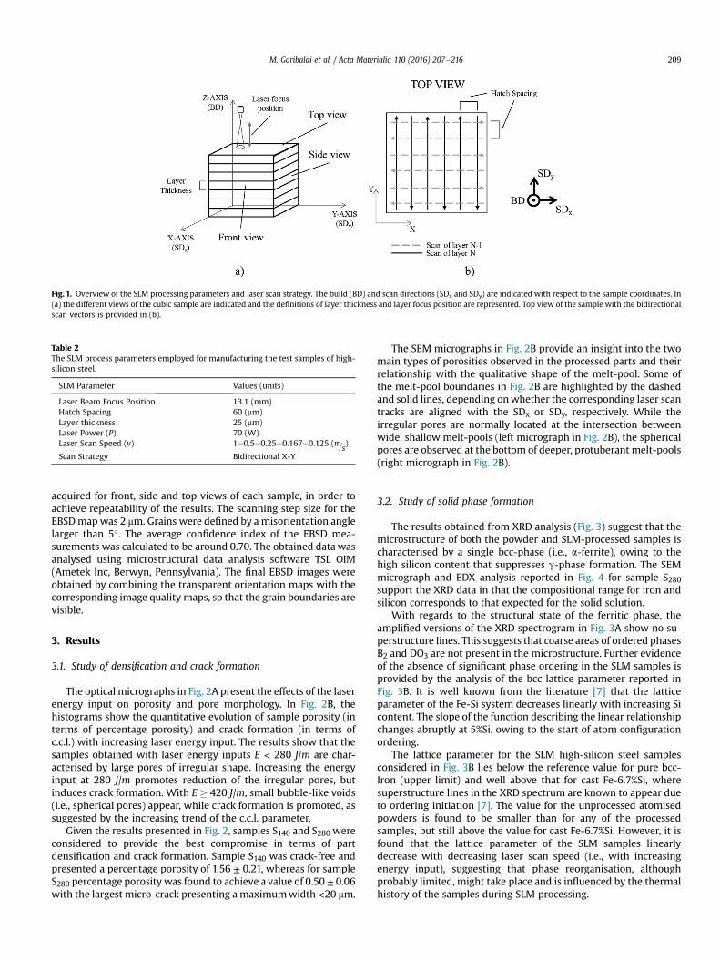
Fig. 1. Overview of the SLM processing parameters and laser scan strategy. The build (BD) and scan directions (SDx and SDy) are indicated with respect to the sample coordinates. In(a) the different views of the cubic sample are indicated and the definitions of layer thickness and layer focus position are represented. Top view of the sample with the bidirectionalscan vectors is provided in (b).
Table 2The SLM process parameters employed for manufacturing the test samples of high-silicon steel.
SLM Parameter Values (units)
Laser Beam Focus Position 13.1 (mm)Hatch Spacing 60 (mm)Layer thickness 25 (mm)Laser Power (P) 70 (W)Laser Scan Speed (v) 1e0.5e0.25e0.167e0.125 (m=s
)
Scan Strategy Bidirectional X-Y
M. Garibaldi et al. / Acta Materialia 110 (2016) 207e216 209
acquired for front, side and top views of each sample, in order toachieve repeatability of the results. The scanning step size for theEBSDmapwas 2 mm. Grains were defined by a misorientation anglelarger than 5�. The average confidence index of the EBSD mea-surements was calculated to be around 0.70. The obtained data wasanalysed using microstructural data analysis software TSL OIM(Ametek Inc, Berwyn, Pennsylvania). The final EBSD images wereobtained by combining the transparent orientation maps with thecorresponding image quality maps, so that the grain boundaries arevisible.
3. Results
3.1. Study of densification and crack formation
The optical micrographs in Fig. 2A present the effects of the laserenergy input on porosity and pore morphology. In Fig. 2B, thehistograms show the quantitative evolution of sample porosity (interms of percentage porosity) and crack formation (in terms ofc.c.l.) with increasing laser energy input. The results show that thesamples obtained with laser energy inputs E < 280 J/m are char-acterised by large pores of irregular shape. Increasing the energyinput at 280 J/m promotes reduction of the irregular pores, butinduces crack formation. With E � 420 J/m, small bubble-like voids(i.e., spherical pores) appear, while crack formation is promoted, assuggested by the increasing trend of the c.c.l. parameter.
Given the results presented in Fig. 2, samples S140 and S280 wereconsidered to provide the best compromise in terms of partdensification and crack formation. Sample S140 was crack-free andpresented a percentage porosity of 1.56 ± 0.21, whereas for sampleS280 percentage porosity was found to achieve a value of 0.50 ± 0.06with the largest micro-crack presenting a maximumwidth <20 mm.
The SEM micrographs in Fig. 2B provide an insight into the twomain types of porosities observed in the processed parts and theirrelationship with the qualitative shape of the melt-pool. Some ofthe melt-pool boundaries in Fig. 2B are highlighted by the dashedand solid lines, depending onwhether the corresponding laser scantracks are aligned with the SDx or SDy, respectively. While theirregular pores are normally located at the intersection betweenwide, shallow melt-pools (left micrograph in Fig. 2B), the sphericalpores are observed at the bottom of deeper, protuberant melt-pools(right micrograph in Fig. 2B).
3.2. Study of solid phase formation
The results obtained from XRD analysis (Fig. 3) suggest that themicrostructure of both the powder and SLM-processed samples ischaracterised by a single bcc-phase (i.e., a-ferrite), owing to thehigh silicon content that suppresses g-phase formation. The SEMmicrograph and EDX analysis reported in Fig. 4 for sample S280support the XRD data in that the compositional range for iron andsilicon corresponds to that expected for the solid solution.
With regards to the structural state of the ferritic phase, theamplified versions of the XRD spectrogram in Fig. 3A show no su-perstructure lines. This suggests that coarse areas of ordered phasesB2 and DO3 are not present in the microstructure. Further evidenceof the absence of significant phase ordering in the SLM samples isprovided by the analysis of the bcc lattice parameter reported inFig. 3B. It is well known from the literature [7] that the latticeparameter of the Fe-Si system decreases linearly with increasing Sicontent. The slope of the function describing the linear relationshipchanges abruptly at 5%Si, owing to the start of atom configurationordering.
The lattice parameter for the SLM high-silicon steel samplesconsidered in Fig. 3B lies below the reference value for pure bcc-Iron (upper limit) and well above that for cast Fe-6.7%Si, wheresuperstructure lines in the XRD spectrum are known to appear dueto ordering initiation [7]. The value for the unprocessed atomisedpowders is found to be smaller than for any of the processedsamples, but still above the value for cast Fe-6.7%Si. However, it isfound that the lattice parameter of the SLM samples linearlydecrease with decreasing laser scan speed (i.e., with increasingenergy input), suggesting that phase reorganisation, althoughprobably limited, might take place and is influenced by the thermalhistory of the samples during SLM processing.

Fig. 2. Effect of processing laser energy input on sample porosity. In a) the optical micrographs of different SLM samples are shown (left), alongside the values of percent porosityand c.c.l. plotted against laser energy input (right). The SEM micrographs in b) show two examples of irregular (left) and spherical pores (right). The dashed and solid lines indicatethe transversal and longitudinal melt-pool cross-sections, respectively.
M. Garibaldi et al. / Acta Materialia 110 (2016) 207e216210
3.3. Study of microstructures
The SEM micrographs in Figs. 5 and 6 provide insights into themicrostructural features of samples S140 and S280 for the top andfront views (please note that the microstructures for the front viewof the samples were also found for the side view and are thereforenot shown here). Fig. 5 shows that the grain boundaries of theprocessed samples are not always clearly identifiable. However, inthe vertical plane the grains appear to present an overall columnarmorphology and are more or less oriented along the BD, suggestingthat epitaxial growth of the grains takes place, according to a grainselection process in which grains whose “easy growth” directions(the <001> family for the bcc system) are oriented along the di-rection of solidification outgrow the less optimally oriented grains.For sample S280 the grains appear more elongated and in somecases span several hundred microns along the BD.
As regards the horizontal plane of the samples, the two micro-graphs at bottom of Fig. 5 show that the grain structure of sampleS280 is coarser than that of sample S140. Furthermore, the grains areequiaxed for sample S140, whereas the grain structure of sampleS280 is more heterogeneous. In particular, two grain morphologiesare of interest in the higher energy input sample. Regions of fine,equiaxed grains (indicated by the letter C in Fig. 5) are found incorrespondence of the scan track centreline. Adjacent to the cen-trelines (which are not always visible owing to melt-pool overlap),
regions of coarser, elongated grains (identified by the letter E inFig. 5) are observed.
From the SEM images in Fig. 5 the melt-pool boundaries are alsovisible and appear to significantly affect the grain structures of thetwo samples considered. In the vertical plane, the transversal melt-pool cross-sections of sample S140 are shallow and flat, whereas inS280 both shallow and protuberant melt-pools are observed, insimilar proportions. Since melt-pool shape determines the orien-tation of the heat flow and consequently the solidification patterns,it significantly affects grain orientation. In this regard, the frontview of the samples in Fig. 5 suggest that in sample S140 the lon-gitudinal melt-pool cross-sections are more irregular than insample S280 and this causes the formation of a more heterogeneousgrain orientation in the former sample.
In order to understand how shallow and protuberant melt-poolsaffect the grain structures, the SEM micrographs in Fig. 6 offer acloser look at the two types of melt-pool shapes for the front viewof the samples. Inside both melt-pool types, the grains are formedby cellular-dendritic solidification substructures that appear as thinstringy features stretching parallel to the longitudinal axis of thegrains. The fact that the cellular substructures become visible uponetching suggests that eccess-solute partitioning into the cellularspacings has occurred during solidification. The orientations of thesolidification substructures in different regions of the melt-poolsare indicated by the arrows in Fig. 6. Inside the shallow melt-

Fig. 3. XRD analysis of SLM high-silicon steel. In a), the main and amplified plots show the XRD spectra for powder and samples S140 and S280. In b) the lattice parameters are shownfor four samples processed using different energy inputs, the powder and the reference values of pure iron and cast Fe-6.7%Si from Ref. [7].
Fig. 4. Grain composition of sample S280 measured by EDX. SEM image of the investigated region (a), EDX spectrum corresponding to region 1 (b), and chemical composition in thethree regions under exam (c).
M. Garibaldi et al. / Acta Materialia 110 (2016) 207e216 211
pools (Fig. 6C and D) the solidification substructures grow mainlyparallel to the BD, regardless of the location within the melt-pool,owing to the almost vertical orientation of the solidification frontnormal.
In the protuberant melt-pools (Fig. 6A and B) the growth pathorientation depends on the location inside the melt-pool. In cor-respondence of the melt-pool centreline the cellular substructuresand corresponding grains are oriented along the BD and growepitaxially. In the regions adjacent to the centreline, growth has
mainly occurred towards the centreline according to the inclinationof the melt-pool boundaries. The grains in this region of the melt-pool correspond, in the horizontal plane of the sample, to theelongated structures identified by the letter E in the image at thebottom-right of Fig. 5. In these regions epitaxial growth along theBD should be hindered by the inclination of the melt-pool bound-ary with respect to the BD. However, since the lateral melt-poolboundaries are oriented more or less along the BD in the protu-berant portion of the melt-pool, the cellular-dendrites growing

Fig. 5. SEM micrographs for the top and front views of samples S140 and S280. The boundaries of some of the melt-pool cross-sections are highlighted by the dashed and solid lines,depending on the orientation. In the top view of sample S280 the letter E and C indicate regions of elongated and equiaxed grains, respectively.
Fig. 6. Cross-sections of deep and shallowmelt-pools in the sample vertical plane. The grain and solidification structures inside deep and shallow melt-pools are visible for partiallyremelted layers (a and c, respectively) and for the top layer (b and d, respectively). The local growth direction of the solidification structures is indicated by the arrows. The dashedlines highlight the melt-pool boundaries.
M. Garibaldi et al. / Acta Materialia 110 (2016) 207e216212
direction in Fig. 5A and B is often observed to shift by angles close to90� in the vertical plane. In these situations the shift does notprompt the nucleation of a new grain since the grain orientation isnot affected, owing to the orthogonality of the lattice vectors in thebcc crystal structure. Therefore, the existing grains can still growacrossmultiplemelt-pools. The samemechanism is observed as thesolidification structures growing from the lateral melt-poolboundaries approach the melt-pool centreline. Here, some grainsare observed to shift their direction of growth abruptly by nearly
90�, as the images in Fig. 5A and B also show.At the top layer of the parts (Fig. 6B and D), the upper portion of
both the deep and shallow melt-pools is characterised by grainsthat have grown almost horizontally, following the direction of thesolidification front, which is almost vertical in that region of themelt-pool. However, for the previous layers the upper part of themelt-pools is remelted when a new layer is deposited and thereforewill disappear from the structure.

M. Garibaldi et al. / Acta Materialia 110 (2016) 207e216 213
3.4. Study of crystallographic texture
EBSD data analysis shows a crystallographic texture in the grainsof SLM high-silicon steel. Fig. 7 shows the resulting PFs of twodifferent samples. These are samples S140 (left-hand plots) and S280(right-hand plots). The PF plots quantify the texture intensities forthe three crystallographic direction families <001>, <101> and<111> with respect to the front view of the sample. Both samplespresent a <001> texture along the BD, which is consistent with themorphological orientation of the columnar grains discussed inSection 3.3. Fig. 7 also shows that the fibre-texture in sample S140 isaltered into a cube-texture by increasing the energy input to 280 J/m. In the cube-textured sample, the <001> axes are aligned withthe BD and, in the scanning plane of the sample, with the directionsrunning approximately halfway between the SDx and SDy. How-ever, a larger spread of the texture is observed around these di-rections than around the BD.
The maximum texture intensity of S280 is found to be almosttwice the maximum intensity of S140. This suggests that the laserenergy input largely affects the intensity of the texture, with alarger energy input producing a more textured sample.
The EBSD maps of sample S280 in Fig. 8 aim at providing anoverview of the correlation between grain morphology and their<001> texture, both along the BD and, in the scanning plane, alongthe bisector of the angle between the SDx and the SDy. The colour-coded EBSD maps for the front view of the sample (Fig. 8A) showthat the majority of the long columnar grains of sample S280 pref-erentially orient their <001> axes along the BD (left image inFig. 8A). This result corroborates the hypothesis of epitaxial graingrowth along the BD. Along the SDx-SDy bisector (right image inFig. 8A), a smaller portion of the grains is red coloured.
In the horizontal plane (Fig. 8C) the majority of the grains arecoloured red when the orientation of the <001> directions isconsidered along the BD (left image in Fig. 8C), regardless of grainmorphology. Conversely, the analysis along the SDx-SDy bisectordirection (right image in Fig. 8C) reveals that there is a correlationbetween the morphology of the grains and their crystallographictexture. In particular, the grains that present an equiaxedmorphology in the horizontal plane tend to be characterised by a<001> texture along the BD only (fibre-texture), whereas a large
Fig. 7. Pole figures (PF) showing the preferred orientation of the <001> crystallographic d
portion of the elongated grains present a <001> texture both alongthe BD and approximately along the SDx-SDy bisector directions(cube-texture). The latter more or less correspond to the orienta-tion directions of the elongated grains. The IPFs (Fig. 8B and D) areconsistent with the EBSD maps in that in the scanning plane thecrystallographic texture is characterised by a lower peak intensityand larger spread than along the BD.
4. Discussion
4.1. Origin of defects
It is known from the literature of SLM alloys that increasing theenergy input promotes densification of the part by improvingpowder melting and reducing melt-pool instabilities (e.g., balling)[17e19]. However, it has been shown in Fig. 2 that while theamount of irregular porosities is reduced with the increase in en-ergy input, the formation of the spherical pores and cracks withincreasing energy input prevents the part from reaching full den-sity. Spherical porosity formation is associated with the transitionbetween different welding modes. The qualitative change of themelt-pool shape from flat to protuberant at high energy inputs, asshown in Fig. 2B, suggests that conduction mode welding isreplaced by key-hole welding [17]. The formation of a key-holeoccurs by surface vaporization of material, thus involving the cre-ation of gas bubbles that can remain trapped inside the melt-poolduring solidification. Furthermore, the dynamics of the Mar-angoni flow increases with laser energy input, thus increasing theprobability of any gas (either newly formed or originally trappedwithin the highly packed powder particles) being dragged towardsthe bottom of the melt-pool [20].
The formation of cracks can be attributed to the thermal stressesinduced during SLM processing. As presented in the literature [21],SLM introduces tensile residual stresses in the part owing to thelocalised application of high energy over a very short time interval(in the order of the ms) which, alongside the poor heat conductivityof the powder bed, develops a high thermal gradient around thelaser spot. Differential expansion takes place and eventually theheat affected zone, whose tendency to expand is inhibited by thesurrounding material, is plastically compressed. During cooling, the
irection for samples S280 and S140 and for three samples views (front, side and top).

Fig. 8. EBSD maps (a and c) and IPFs (b and d) for the front and top views of sample S280. The maps/IPFs on the left of each frame show the texture found along the BD. The maps andIPFs on the right of each frame show the texture along the bisector of the angle formed by SDx and SDy. The white arrows in the EBSD image for the top view indicate the directionsof two laser scan tracks that are still visible.
M. Garibaldi et al. / Acta Materialia 110 (2016) 207e216214
upper layer's tendency to contract is again counteracted by theunderlying layers, thus creating tensile stresses. In the presentstudy, cracks propagate more or less parallel to the scanning plane(i.e., the horizontal plane), as observed in Fig. 2A. On the otherhand, inter-granular crack propagation has not been observed andthis is probably linked to the absence of significant macro-segregation phenomena at the grain boundaries.
4.2. Origin of solid phase formation
The results from the XRD analysis presented in Fig. 3 can beexplained by considering the extremely high cooling rates (nor-mally varying from 103 up to 106 K/s in laser welding [22]) at whichthe material solidifies during SLM processing. Such fast cooling,often results in non-equilibrium phase formation, i.e., the binaryFe-Si system is “frozen” into the disordered solid solution. The
order of magnitude of the cooling rates during gas-atomisation iscomparable to those reached during SLM, thus explaining therelatively high lattice parameter value of the LPW powder withrespect to cast Fe-6.7%Si. Literature results [23] suggest that tosuppress the B2 ordered phase when the concentration of Si is 5.6%,an average cooling rate of 340 K/s is necessary. Therefore, the highaverage cooling rates achieved during SLM processing can reason-ably be expected to lie beyond the ordering suppression threshold.
The suppression of the ordered phases B2 and DO3 can bebeneficial, since it makes silicon steels less brittle and electricallyconductive [9,23]. The at least partial suppression of phase orderingmight be another advantageous aspect of using SLM for processinghigh-silicon steel. However, it should be noted that XRD alone isgenerally not sufficient to characterise phase ordering. As discussedin section 3.3, the processed parts are characterised by fine cellulargrain substructures and by visible melt-pool boundaries. These

M. Garibaldi et al. / Acta Materialia 110 (2016) 207e216 215
featuresmight indicatemicro-segregation sites where intermetallicFe3Si could have potentially precipitated.
4.3. Origin of texture
The comparison between samples S140 and S280 has shown thatdoubling the laser energy input promotes columnar grain forma-tion (Fig. 5) and intensifies the crystallographic texture along theBD (Fig. 7). The dependency of morphological and crystallographictexture intensities on laser energy input in SLM-processed partshad already been reported by the authors of [12], which found thatby replacing a 400 W laser beam source with a 1000 W one, themorphological and crystallographic textures of an SLM austeniticstainless steel could be remarkably increased. The relationship canbe explained by the increased amount of partial remelting and, asshown in Fig. 5, by the improved smoothness of the depositedlayers. These phenomena both occur when the energy input of thescanning laser is increased. Partial remelting of the grains whosecrystallographic directions of “easy growth” (the <001> family inbcc systems) orient along the BD provides a substrate for the newlyprocessed material to solidify epitaxially, as well-known fromweldmetal solidification theory [22]. Clearly, a greater amount of opti-mally oriented grains will result in stronger texture intensities.
Fig. 7 has also shown that increasing the energy input from140 J/m to 280 J/m also alters the <001> fibre-texture into a cubic-texture, characterised by the tendency of the <001> axes to orientboth along the BD and more or less along the direction of theSDx�SDy bisector. This has been associated to the appearance ofdeeper, protuberant melt-pools, whose solidification front is almosthorizontal at the melt-pool centreline, but shifts its direction to-wards the BD at the melt-pool sides. The protuberant melt-poolshape determines a shift in the growth direction of the cellular-dendritic solidification structures of nearly 90� in the verticalplane with respect to the BD, as the images in Fig. 6A and B haveshown. The 90� shift in the growth direction is attributed to theorthogonality of the axes in the bcc system, which causes thecrystallographic axis of the <001> family closer to the thermalgradient direction to be activated at the lateral boundaries of themelt-pool, thus allowing the underlying grain to grow across themelt-pool boundary horizontally.
In the scanning plane, the solidification structures that havegrown almost horizontally have produced grains characterised byan elongated cross-section and oriented following the solidificationfront normal (refer to the grains identified by the letter E in Fig. 5).Importantly, the morphological orientation has also prompted acrystallographic texture, and the EBSD results (Figs. 7 and 8) haveshown that in the scanning plane the <001> crystallographic axestend to align along a range of directions close to the SDx-SDybisector, following the morphological orientation of the grains. Theformation of a cube-texture for an SLM alloy is reported in theliterature [13], where it is attributed to the employment of a bidi-rectional X-Y scan strategy. While in the present study the forma-tion of the cube-texture is attributed to the morphology of themelt-pool, understanding the effect of the scanning strategy onthe development of the crystallographic texture would be of greatinterest. Unfortunately, a more extensive exploration of the effect ofthe SLM-process design space on the texture of the samples hasbeen, to this date, limited by the alloy's brittle nature, which makesthe creation of near-fully dense parts a challenge.
It is finally noteworthy that the nature of the specific alloy underinvestigation promotes texture formation, since the high siliconcontent suppresses g-phase formation from the phase diagramthus leaving no secondary phase to hinder ferritic graindevelopment.
5. Conclusions
The main findings of this research can be summarised in thefollowing points:
- Near-fully dense high-silicon steel three-dimensional partswere manufactured using SLM for the first time in this work,starting from pre-alloyed powder;
- The SLM high-silicon steel is a single ferritic phase and super-structure lines could not be observed from the XRD measure-ments, suggesting the fast cooling rates of SLM retard phaseordering formation;
- The microstructure of the samples is characterised by columnargrains oriented towards the BD. Increasing the processing laserenergy input seems to promote grain elongation both along theBD and in the scanning plane of the sample;
- By increasing the laser energy input, a crystallographic <001>fibre-texture can be altered into a cube-texture. This has beenassociated with a change in the qualitative shape of the melt-pool from shallow to protuberant.
In conclusion, this research has shown that SLM might poten-tially open the path to an alternative route for the manufacture ofgrain-oriented high-silicon steels for magnetic applications, sincethe <001> directions are the so-called “easy axes” of magnet-isation. How the metallurgy affects the magnetic properties is thesubject of ongoing research.
Acknowledgements
The research leading to these results has received funding fromthe People Programme (Marie Curie Actions) of the EuropeanUnion’0073 Seventh Framework Programme (FP7/2007-2013) un-der REA grant agreement no 608322.
References
[1] N. Hopkinson, R. Hague, P. Dickens, Rapid Manufacturing: an Industrial Rev-olution for the Digital Age, John Wiley & Sons, 2006.
[2] M. Rombouts, J.-P. Kruth, L. Froyen, P. Mercelis, Fundamentals of selectivelaser melting of alloyed steel powders, CIRP Ann-Manuf Technol. 55 (2006)187e192.
[3] L. Thijs, F. Verhaeghe, T. Craeghs, J. Van Humbeeck, J.-P. Kruth, A study of themicrostructural evolution during selective laser melting of Tie6Ale4V, ActaMater 58 (2010) 3303e3312.
[4] B. Vandenbroucke, J.-P. Kruth, Selective laser melting of biocompatible metalsfor rapid manufacturing of medical parts, Rapid Prototyp. J. 13 (2007)196e203.
[5] E. Louvis, P. Fox, C.J. Sutcliffe, Selective laser melting of aluminium compo-nents, J. Mater Process Technol. 211 (2011) 275e284.
[6] B. Zhang, N.-E. Fenineche, H. Liao, C. Coddet, Microstructure and magneticproperties of FeeNi alloy fabricated by selective laser melting Fe/Ni mixedpowders, J Mater Sci Technol 29 (2013) 757e760.
[7] R.M. Bozorth, Ferromagnetism, Wiley-VCH, 1993.[8] M. Namikawa, H. Ninomiya, T. Yamaji, High silicon steel sheets realizing
excellent high frequency reactor performance, JFE Tech. Rep. 6 (2005) 12e17.[9] P. Jang, B. Lee, G. Choi, Effects of annealing on the magnetic properties of
Fee6.5% Si alloy powder cores, J. Appl. Phys. 103 (2008), 07E743.[10] H.-T. Liu, Z.-Y. Liu, Y.-Q. Qiu, Y. Sun, G.-D. Wang, Microstructure, texture and
magnetic properties of strip casting Fee6.2 wt% Si steel sheet, J. Mater ProcessTechnol. 212 (2012) 1941e1945.
[11] X. He, X. Li, Y. Sun, Microstructure and magnetic properties of high siliconelectrical steel produced by electron beam physical vapor deposition, J. Magn.Magn. Mater 320 (2008) 217e221.
[12] T. Niendorf, S. Leuders, A. Riemer, H.A. Richard, T. Tr€oster, D. Schwarze, Highlyanisotropic steel processed by selective laser melting, Metall. Mater Trans. B44 (2013) 794e796.
[13] L. Thijs, K. Kempen, J.-P. Kruth, J. Van Humbeeck, Fine-structured aluminiumproducts with controllable texture by selective laser melting of pre-alloyedAlSi10Mg powder, Acta Mater 61 (2013) 1809e1819.
[14] R. Hilzinger, W. Rodewald, Magnetic materials, Vacuumschmelze, 2013.[15] P. Beckley, Electrical Steels for Rotating Machines, IET, 2002.[16] http://imagej.net [as on 08/02/2016].

M. Garibaldi et al. / Acta Materialia 110 (2016) 207e216216
[17] N.B. Dahotre, S. Harimkar, Laser Fabrication and Machining of Materials,Springer Science and Business Media, New York, USA, 2008.
[18] I. Yadroitsev, P. Bertrand, I. Smurov, Parametric analysis of the selective lasermelting process, Appl. Surf. Sci. 253 (2007) 8064e8069.
[19] N.T. Aboulkhair, N.M. Everitt, I. Ashcroft, C. Tuck, Reducing porosity inAlSi10Mg parts processed by selective laser melting, Addit. Manuf. 1 (2014)77e86.
[20] G. Ng, A. Jarfors, G. Bi, H. Zheng, Porosity formation and gas bubble retention
in laser metal deposition, Appl. Phys. A 97 (2009) 641e649.[21] H. Pohl, A. Simchi, M. Issa, H.C. Dias, Thermal stresses in direct metal laser
sintering, in: 12th Solid Freeform Fabrication Symposium, Austin, TX, 2001.[22] S. David, J. Vitek, Correlation between solidification parameters and weld
microstructures, Int. Mater Rev. 34 (1989) 213e245.[23] J. Shin, J. Bae, H. Kim, H. Lee, T. Lee, E. Lavernia, Z. Lee, Orderingedisordering
phenomena and micro-hardness characteristics of B2 phase in Fee(5e6.5%) Sialloys, Mater Sci. Eng. A 407 (2005) 282e290.