measurement 3. testing of logical network built from
TRANSCRIPT

1
Measurement 3.
Testing of logical network built from functional elements
The aim of the laboratory is to practice locating the failures in a logical network. The logic
network realizes a reaction time measurement instrument (RIM). The instrument is realized on a
SPARTAN 3 FPGA.
The instrument is controlled by 3 buttons. The Start button (BTN3) starts the measurement -
when pressed, either the left side LED (LD7) or the right side LED (LD0) will be turned on and a
4-digit decimal counter-chain starts to count from 0000 state. The state of the counter-chain is
displayed on the time multiplexed 4 digit 7 segment LED display. The rate of the counting is 1
msec. Counting can be stopped by pressing the appropriate button: SWL (left side button) or
SWR (right side button). The display shows the elapsed time since the pressing of the START
button; counting stops when the appropriate side button (SWL or SWR) is pressed. If neither
SWL nor SWR is pressed, counting is automatically stopped when 9999 is reached. The counter
can be reset by the RESET button (BTN2).
START-STOP
divider
BCD counterLED
4 digits
7 segments
display
random
generator
Q0
t1msec
MEAS
CLEAR
Q0
L_RSWL SWR
LD_L LD_R
clk(50MHz)
clk
clk
L_R
START
chain
unit
Simplified functional diagram
The place of the buttons and the LEDs on the FPGA panel
2
The operation of the instrument (see the schematic on the last page)
The divider unit divides the 50MHz clock signal by 50000 and activates the t1msec signal once
in every 1msec. The width of this signal is 20nsec (1 period of the 50MHz clock signal).
The random generator unit produces the logical level of the L_R signal randomly, and activates
the LD_L or LD_R signal depending on the L_R signal. The least significant bit of the divider
counter is sampled by a D flip-flop. The D flip-flop is disabled when the measuring is started
(MEAS signal), so the state of the D flip-flop (L_R) is random.
The START-STOP unit is responsible for resetting the counter (CLEAR signal); enabling or
stopping the counter (MEAS signal). The START-STOP unit consists of 2 parts: a state machine
and a stp_cond combinational network.
The stp_cond module generates the P signal; this signal is active when the signal generated by
pressing the appropriate button is activated or the counter reaches 9999 (indicated by the OVR
signal). SE will be active when SWL and SWR buttons (signals) are inactive, to avoid the
swindle.
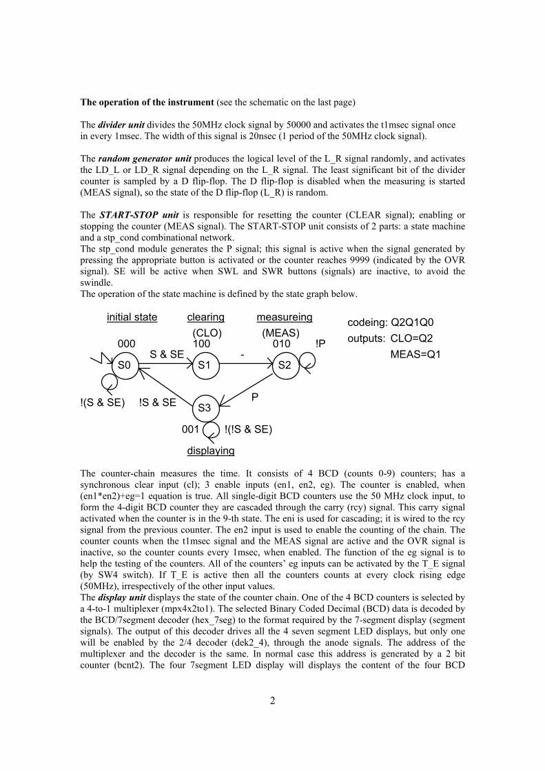
The operation of the state machine is defined by the state graph below.
000 100 010
001
S0 S1 S2
S3
S & SE
P!S & SE
-
!(S & SE)
!P
!(!S & SE)
codeing: Q2Q1Q0
CLO=Q2
MEAS=Q1
outputs:(CLO) (MEAS)
clearing measureing
displaying
initial state
The counter-chain measures the time. It consists of 4 BCD (counts 0-9) counters; has a
synchronous clear input (cl); 3 enable inputs (en1, en2, eg). The counter is enabled, when
(en1*en2)+eg=1 equation is true. All single-digit BCD counters use the 50 MHz clock input, to
form the 4-digit BCD counter they are cascaded through the carry (rcy) signal. This carry signal
activated when the counter is in the 9-th state. The eni is used for cascading; it is wired to the rcy
signal from the previous counter. The en2 input is used to enable the counting of the chain. The
counter counts when the t1msec signal and the MEAS signal are active and the OVR signal is
inactive, so the counter counts every 1msec, when enabled. The function of the eg signal is to
help the testing of the counters. All of the counters’ eg inputs can be activated by the T_E signal
(by SW4 switch). If T_E is active then all the counters counts at every clock rising edge
(50MHz), irrespectively of the other input values.
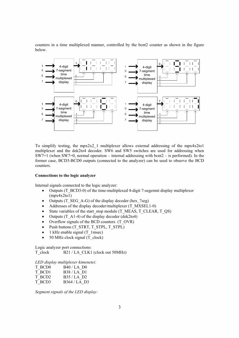
The display unit displays the state of the counter chain. One of the 4 BCD counters is selected by
a 4-to-1 multiplexer (mpx4x2to1). The selected Binary Coded Decimal (BCD) data is decoded by
the BCD/7segment decoder (hex_7seg) to the format required by the 7-segment display (segment
signals). The output of this decoder drives all the 4 seven segment LED displays, but only one
will be enabled by the 2/4 decoder (dek2_4), through the anode signals. The address of the
multiplexer and the decoder is the same. In normal case this address is generated by a 2 bit
counter (bcnt2). The four 7segment LED display will displays the content of the four BCD
3
counters in a time multiplexed manner, controlled by the bcnt2 counter as shown in the figure
below.
4-digit
7-segment
time
multiplexed
display
4-digit
7-segment
time
multiplexed
display
4-digit
7-segment
time
multiplexed
display
4-digit
7-segment
time
multiplexed
display
To simplify testing, the mpx2x2_1 multiplexer allows external addressing of the mpx4x2to1
multiplexer and the dek2to4 decoder. SW6 and SW5 switches are used for addressing when
SW7=1 (when SW7=0, normal operation – internal addressing with bcnt2 – is performed). In the
former case, BCD3-BCD0 outputs (connected to the analyzer) can be used to observe the BCD
counters.
Connections to the logic analyzer
Internal signals connected to the logic analyzer:
• Outputs (T_BCD3-0) of the time-multiplexed 4-digit 7-segemnt display multiplexer
(mpx4x2to1)
• Outputs (T_SEG_A-G) of the display decoder (hex_7seg)
• Addresses of the display decoder/multiplexer (T_MXSEL1-0)
• State variables of the start_stop module (T_MEAS, T_CLEAR, T_QS)
• Outputs (T_A1-4) of the display decoder (dek2to4)
• Overflow signals of the BCD counters (T_OVR)
• Push buttons (T_STRT, T_STPL, T_STPL)
• 1 kHz enable signal (T_1msec)
• 50 MHz clock signal (T_clock)
Logic analyzer port connections:
T_clock B21 / LA_CLK1 (clock out 50MHz)
LED display multiplexer kimenetei:
T_BCD0 B40 / LA_D0
T_BCD1 B38 / LA_D1
T_BCD2 B35 / LA_D2
T_BCD3 B364 / LA_D3
Segment signals of the LED display:

4
T_SEG_A B33 / LA_D4
T_SEG_B B32 / LA_D5
T_SEG_C B31 / LA_D6
T_SEG_D B30 / LA_D7
T_SEG_E B29 / LA_D8
T_SEG_F B28 / LA_D9
T_SEG_G B27 / LA_D10
START_STOP state machine:
T_MEAS B26 / LA_D11
T_CLEAR B25 / LA_D12
T_QS B24 / LA_D13
Overflow signal of the counter chain:
T_OVR B14 / LA_D14
1msec-os counter enable signal:
T_t1msec D23 / LA_CLK2
Switches:
T_STRT B22 / LA_D15
T_STPL B20 / LA_D16
T_STPR B19 / LA_D17
Outputs of the display decoder:
T_A1 B18 / LA_D18
T_A2 B17 / LA_D19
T_A3 B16 / LA_D20
T_A4 B15 / LA_D21
Address signals of the display decoder/multiplexer:
T_MXSEL0 B14 / LA_D22
T_MXSEL1 B13 / LA_D23

5
1. Functional checking of the RIM
1.1. First you get a failure-free configuration file from the instructor (rim.bit). Download the file to the FPGA board and study the operation of the RIM!
1.2. Second you will get a configuration file with some failures (rimij.bit). Download the file to the FPGA board and study the operation of the RIM and write down the differences from the
normal operation.
2. Finding failures on the RIM
2.1. On the basis of the founded deviations, try to locate the functional units which contain the failures and try to guess the kind of the failures!
2.2. Select one of the suspicious units and check the operation of the unit by logic analyzer! 2.3. Ask the instructor for the Verilog description of the suspicious unit. Locate and correct the
problem in the module. Give back the corrected module to the instructor. The instructor will
generate a new configuration file using the corrected module and give it back to you.
2.4. Download the corrected file to the FPGA board and continue the work till the operation of the RIM is entirely correct. Write down all the founded failures and the way you found them.
If you use logic analyzer to find a failure, insert a screenshot into the documentation which
shows the appropriate waveform diagram!

6