mcp73861/2/3/4 data sheet
TRANSCRIPT

MCP73861/2/3/4Advanced Single or Dual Cell, Fully Integrated Li-Ion/Li-Polymer
Charge Management Controllers
Features:• Linear Charge Management Controllers:
- Integrated Pass Transistor- Integrated Current Sense- Reverse-Blocking Protection
• High-Accuracy Preset Voltage Regulation: + 0.5% • Four Selectable Voltage Regulation Options:
- 4.1V, 4.2V – MCP73861/3- 8.2V, 8.4V – MCP73862/4
• Programmable Charge Current: 1.2A Maximum• Programmable Safety Charge Timers• Preconditioning of Deeply Depleted Cells• Automatic End-of-Charge Control• Optional Continuous Cell Temperature Monitoring• Charge Status Output for Direct LED Drive• Fault Output for Direct LED Drive• Automatic Power-Down• Thermal Regulation• Temperature Range: -40°C to +85°C• Packaging: 16-Pin, 4 x 4 QFN
16-Pin SOIC
Applications:• Lithium-Ion/Lithium-Polymer Battery Chargers• Personal Data Assistants (PDAs)• Cellular Telephones• Hand-Held Instruments• Cradle Chargers• Digital Cameras• MP3 Players
Description:The MCP7386X family of devices features highlyadvanced linear charge management controllers foruse in space-limited, cost-sensitive applications. Thedevices combine high-accuracy, constant voltage andcurrent regulation, cell preconditioning, celltemperature monitoring, advanced safety timers,automatic charge termination, internal current sensing,reverse-blocking protection, charge status and faultindication in either a space-saving 16-pin 4 x 4 QFNpackage, or a 16-pin SOIC package. The MCP7386Xprovides a complete, fully functional, stand-alonecharge management solution with a minimum numberof external components.
The MCP73861/3 is intended for applications utilizingsingle-cell Lithium-Ion or Lithium-Polymer batterypacks, while the MCP73862/4 is intended for dualseries cell Lithium-Ion or Lithium-Polymer batterypacks. The MCP73861/3 has two selectablevoltage-regulation options available (4.1V and 4.2V),for use with either coke or graphite anodes and operatewith an input voltage range of 4.5V to 12V. TheMCP73862/4 has two selectable voltage-regulationoptions available (8.2V and 8.4V), for use with coke orgraphite anodes, and operate with an input voltagerange of 8.7V to 12V.The MCP73861/2 and MCP73863/4 differ only in thefunction of the charge status output (STAT1) when acharge cycle has been completed. The MCP73861/2flashes the output, while the MCP73863/4 turns theoutput off. Refer to Section 5.2.1 “Charge StatusOutputs (STAT1, STAT2)”.The MCP7386X family of devices are fully specifiedover the ambient temperature range of -40°C to +85°C.
2004-2013 Microchip Technology Inc. DS21893F-page 1

MCP73861/2/3/4
Package TypesVDD1
VBAT3
THERM
EN
TIMER
STAT1
STAT2 1
2
3
4
14
15
16
PROG
VDD2
VSET
VSS1
THREF
VBAT1
VBAT2
5
6
7
8 9
10
11
12
13
VSS2
VSS3
16-Pin SOIC16-Pin QFN
2VDD2
VSS1
VSET VBAT3
VBAT2
PR
OG
VBAT1
THR
EF
THER
M
TIM
ER
VSS3S
TAT1
STA
T2E
N
VS
S2
VDD2 EP
161
15 14 13
3
4
12
1110
95 6 7 8
17
DS21893F-page 2 2004-2013 Microchip Technology Inc.

MCP73861/2/3/4
Typical ApplicationFunctional Block Diagram
ENSTAT1STAT2
VSET
VDD
VSS
TIMERPROG
THERMTHREF
VBAT3VBAT
+–
Single Lithium-Ion Cell
2, 31
MCP73861/3
5
6784, 9, 13
10, 1112
141615
5V
6.19 kΩ
4.7µF
1.2A Lithium-Ion Battery Charger
4.7 µF
7.32 kΩ0.1µF Note: Pin numbers shown are for QFN
package. Please refer to Section 6.0 “Applications” for details.
+–
Charge Termination Comparator
Voltage Control Amplifier
+–
UVLO COMPARATOR
VUVLO
+–
Temperature Comparators
+–
Bias and Reference Generator
VUVLO VREF (1.2V)
Power-OnDelay
+
–
+–
VREF
VREF
Oscillator
IREG/12
Constant-Voltage/Recharge Comp.
Precondition Control
Charge_OKPrecon
VDD
Charge Current Control Amplifier
+
–
VREF
VREF
+–
Precondition Comp.
Charge Control,Charge Timers And Status Logic Drv Stat 2
Drv Stat 1
Charge_OK
IREG/12
VDD1
THERM
EN
TIMER
STAT1
STAT2
VBAT3
VSS1
PROG
VSET
THREF
VBAT1
90
110 kΩ
10 kΩ
10 kΩ
100 kΩ
50 kΩ
50 kΩ
G = 0.001
11 kΩ
1 kΩ
600 kΩ(1.65 MΩ)
148.42 kΩ
1.58 kΩ
VDD2 VBAT2
300.04 kΩ
10.3 kΩ(8.58 kΩ)
4 kΩ
Direction Control
kΩ
VSS2VSS3
Values in ( ) reflect the MCP73862/4 devices
2004-2013 Microchip Technology Inc. DS21893F-page 3

MCP73861/2/3/4
1.0 ELECTRICAL CHARACTERISTICS
Absolute Maximum Ratings†VDDN...............................................................................13.5VVBATN, VSET, EN, STAT1, STAT2 w.r.t. VSS.................................................................-0.3 to (VDD + 0.3)VPROG, THREF, THERM, TIMER w.r.t. VSS............. -0.3 to 6VMaximum Junction Temperature, TJ ............ Internally LimitedStorage temperature .....................................-65°C to +150°CESD protection on all pins:
Human Body Model (1.5 kΩ in series with 100 pF)4 kVMachine Model (200 pF, No series resistance) ...........300V
† Notice: Stresses above those listed under “MaximumRatings” may cause permanent damage to the device. This isa stress rating only and functional operation of the device atthose or any other conditions above those indicated in theoperational listings of this specification is not implied.Exposure to maximum rating conditions for extended periodsmay affect device reliability.
DC CHARACTERISTICSElectrical Specifications: Unless otherwise indicated, all limits apply for VDD= [VREG(typ.) + 0.3V] to 12V, TA = -40°C to +85°C. Typical values are at +25°C, VDD = [VREG (typ.) + 1.0V]
Parameters Sym. Min. Typ. Max. Units Conditions
Supply InputSupply Voltage VDD 4.5 — 12 V MCP73861/3
8.7 — 12 V MCP73862/4Supply Current ISS — 0.17 4 µA Disabled
— 0.53 4 mA OperatingUVLO Start Threshold VSTART 4.25 4.5 4.65 V MCP73861/3
8.45 8.8 9.05 V MCP73862/4VDD Low-to-High
UVLO Stop Threshold VSTOP 4.20 4.4 4.55 V MCP73861/38.40 8.7 8.95 V MCP73862/4
VDD High-to-LowVoltage Regulation (Constant-Voltage Mode)Regulated Output Voltage VREG 4.079 4.1 4.121 V MCP73861/3, VSET = VSS
4.179 4.2 4.221 V MCP73861/3,VSET = VDD
8.159 8.2 8.241 V MCP73862/4, VSET = VSS
8.358 8.4 8.442 V MCP73862/4, VSET = VDD
VDD = [VREG(typ.) + 1V], IOUT = 10 mA TA = -5°C to +55°C
Line Regulation ΔVBAT/VBAT)| /ΔVDD
— 0.025 0.25 %/V VDD = [VREG(typ.)+1V] to 12VIOUT = 10 mA
Load Regulation ΔVBAT/VBAT|
— 0.01 0.25 % IOUT = 10 mA to 150 mAVDD = [VREG(typ.)+1V]
Supply Ripple Attenuation PSRR — 60 — dB IOUT = 10 mA, 10 Hz to 1 kHz— 42 — dB IOUT = 10 mA, 10 Hz to 10 kHz— 28 — dB IOUT = 10 mA, 10 Hz to 1 MHz
Output Reverse LeakageCurrent
IDISCHARGE — 0.23 1 µA VDD < VBAT = VREG(typ.), VDD = 1.5 kΩ to Ground
Output Reverse Leakage Switchover Time
IDISCHARGE_SW
— 0 1000 ms VDD < VBAT, VDD <= 1.5 kΩ to Ground
DS21893F-page 4 2004-2013 Microchip Technology Inc.

MCP73861/2/3/4
Current Regulation (Fast Charge Constant-Current Mode)Fast Charge CurrentRegulation
IREG 85 100 115 mA PROG = OPEN1020 1200 1380 mA PROG = VSS
425 500 575 mA PROG = 1.6 kΩTA= -5°C to +55°C
Preconditioning Current Regulation (Trickle Charge Constant-Current Mode)Precondition CurrentRegulation
IPREG 5 10 15 mA PROG = OPEN60 120 180 mA PROG = VSS
25 50 75 mA PROG = 1.6 kΩTA=-5°C to +55°C
Precondition ThresholdVoltage
VPTH 2.70 2.80 2.90 V MCP73861/3, VSET = VSS
2.75 2.85 2.95 V MCP73861/3, VSET = VDD
5.40 5.60 5.80 V MCP73862/4, VSET = VSS
5.50 5.70 5.90 V MCP73862/4, VSET = VDD
VBAT Low-to-HighCharge TerminationCharge Termination Current
ITERM 6 8.5 11 mA PROG = OPEN70 90 120 mA PROG = VSS
32 41 50 mA PROG = 1.6 kΩTA=-5°C to +55°C
Automatic RechargeRecharge Threshold Voltage
VRTH VREG -300 mV VREG -200 mV VREG -100 mV V MCP73861/3VREG -600 mV VREG -400 mV VREG -200 mV V MCP73862/4
VBAT High-to-LowThermistor ReferenceThermistor ReferenceOutput Voltage
VTHREF 2.475 2.55 2.625 V TA = 25°C, VDD = VREG(typ.) + 1V,ITHREF = 0 mA
Thermistor Reference Source Current
ITHREF 200 — — µA
Thermistor Reference Line Regulation
ΔVTHREF/VTHREF)|/ΔVDD
— 0.1 0.25 %/V VDD = [VREG(typ.) + 1V] to 12V
Thermistor Reference Load Regulation
ΔVTHREF/VTHREF|
0.01 0.10 % ITHREF = 0 mA to 0.20 mA
Thermistor ComparatorUpper Trip Threshold VT1 1.18 1.25 1.32 VUpper Trip Point Hysteresis VT1HYS — -50 — mVLower Trip Threshold VT2 0.59 0.62 0.66 VLower Trip Point Hysteresis VT2HYS — 80 — mVInput Bias Current IBIAS — — 2 µAStatus Indicator – STAT1, STAT2Sink Current ISINK 4 8 12 mALow Output Voltage VOL — 200 400 mV ISINK = 1 mAInput Leakage Current ILK — 0.01 1 µA ISINK = 0 mA, VSTAT1,2 = 12V
DC CHARACTERISTICS (CONTINUED)Electrical Specifications: Unless otherwise indicated, all limits apply for VDD= [VREG(typ.) + 0.3V] to 12V, TA = -40°C to +85°C. Typical values are at +25°C, VDD = [VREG (typ.) + 1.0V]
Parameters Sym. Min. Typ. Max. Units Conditions
2004-2013 Microchip Technology Inc. DS21893F-page 5

MCP73861/2/3/4
TEMPERATURE SPECIFICATIONS
Enable InputInput High Voltage Level VIH 1.4 — — VInput Low Voltage Level VIL — — 0.8 VInput Leakage Current ILK — 0.01 1 µA VENABLE = 12VThermal ShutdownDie Temperature TSD — 155 — °CDie Temperature Hysteresis
TSDHYS — 10 — °C
DC CHARACTERISTICS (CONTINUED)Electrical Specifications: Unless otherwise indicated, all limits apply for VDD= [VREG(typ.) + 0.3V] to 12V, TA = -40°C to +85°C. Typical values are at +25°C, VDD = [VREG (typ.) + 1.0V]
Parameters Sym. Min. Typ. Max. Units Conditions
AC CHARACTERISTICSElectrical Specifications: Unless otherwise indicated, all limits apply for VDD = [VREG (typ.) + 0.3V] to 12V, TA = -40°C to +85°C. Typical values are at +25°C, VDD = [VREG (typ.) + 1.0V]
Parameters Sym. Min. Typ. Max. Units Conditions
UVLO Start Delay tSTART — — 5 ms VDD Low-to-HighCurrent RegulationTransition Time Out of Preconditioning
tDELAY — — 1 ms VBAT < VPTH to VBAT > VPTH
Current Rise Time Out of Preconditioning
tRISE — — 1 ms IOUT Rising to 90% of IREG
Fast Charge Safety Timer Period
tFAST 1.1 1.5 1.9 Hours CTIMER = 0.1 µF
Preconditioning Current RegulationPreconditioning Charge Safety Timer Period
tPRECON 45 60 75 Minutes CTIMER = 0.1 µF
Charge TerminationElapsed Time Termination Period
tTERM 2.2 3 3.8 Hours CTIMER = 0.1 µF
Status IndicatorsStatus Output turn-off tOFF — — 200 µs ISINK = 1 mA to 0 mAStatus Output turn-on tON — — 200 µs ISINK = 0 mA to 1 mA
Electrical Specifications: Unless otherwise indicated, all limits apply for VDD = [VREG (typ.) + 0.3V] to 12V.Typical values are at +25°C, VDD = [VREG (typ.) + 1.0V]
Parameters Sym. Min. Typ. Max. Units Conditions
Temperature RangesSpecified Temperature Range TA -40 — +85 °COperating Temperature Range TJ -40 — +125 °CStorage Temperature Range TA -65 — +150 °CThermal Package ResistancesThermal Resistance, 16-lead, 4 mm x 4 mm QFN
JA — 47 — °C/W 4-Layer JC51-7 Standard Board, Natural Convection
Thermal Resistance, 16-lead SOIC JA — 86.1 — °C/W 4-Layer JC51-7 Standard Board, Natural Convection
DS21893F-page 6 2004-2013 Microchip Technology Inc.

MCP73861/2/3/4
2.0 TYPICAL PERFORMANCE CURVES
NOTE: Unless otherwise indicated, VDD = [VREG(typ.) + 1V], IOUT = 10 mA and TA= +25°C, Constant-voltage mode.
FIGURE 2-1: Battery Regulation Voltage (VBAT) vs. Charge Current (IOUT).
FIGURE 2-2: Battery Regulation Voltage (VBAT) vs. Supply Voltage (VDD).
FIGURE 2-3: Battery Regulation Voltage (VBAT) vs. Supply Voltage (VDD).
FIGURE 2-4: Supply Current (ISS) vs. Charge Current (IOUT).
FIGURE 2-5: Supply Current (ISS) vs. Supply Voltage (VDD).
FIGURE 2-6: Supply Current (ISS) vs. Supply Voltage (VDD).
Note: The graphs and tables provided following this note are a statistical summary based on a limited number ofsamples and are provided for informational purposes only. The performance characteristics listed hereinare not tested or guaranteed. In some graphs or tables, the data presented may be outside the specifiedoperating range (e.g., outside specified power supply range) and therefore outside the warranted range.
4.193
4.195
4.197
4.199
4.201
4.203
4.205
4.207
10 100 1000
Charge Current (mA)
Bat
tery
Reg
ulat
ion
Volta
ge (V
)
MCP73861/3VSET = VDDVDD = 5.2V
3.80
3.90
4.00
4.10
4.20
4.30
4.40
4.5 6.0 7.5 9.0 10.5 12.0
Supply Voltage (V)
Bat
tery
Reg
ulat
ion
Volta
ge (V
)
MCP73861/3VSET = VDD
IOUT = 1000 mA
4.193
4.195
4.197
4.199
4.201
4.203
4.205
4.207
4.5 6.0 7.5 9.0 10.5 12.0
Supply Voltage (V)
Bat
tery
Reg
ulat
ion
Volta
ge (V
)
MCP73861/3VSET = VDDIOUT = 10 mA
0.40
0.50
0.60
0.70
0.80
0.90
1.00
10 100 1000
Charge Current (mA)
Supp
ly C
urre
nt (m
A)
MCP73861/3VSET = VDDVDD = 5.2V
0.40
0.60
0.80
1.00
1.20
1.40
1.60
4.5 6.0 7.5 9.0 10.5 12.0
Supply Voltage (V)
Supp
ly C
urre
nt (m
A)
MCP73861/3VSET = VDD
IOUT = 1000 mA
0.40
0.50
0.60
0.70
0.80
0.90
1.00
4.5 6.0 7.5 9.0 10.5 12.0
Supply Voltage (V)
Supp
ly C
urre
nt (m
A)
MCP73861/3VSET = VDD
IOUT = 10 mA
2004-2013 Microchip Technology Inc. DS21893F-page 7

MCP73861/2/3/4
NOTE: Unless otherwise indicated, VDD = [VREG(typ.) + 1V], IOUT = 10 mA and TA= +25°C, Constant-voltage mode.FIGURE 2-7: Output Leakage Current (IDISCHARGE) vs. Battery Regulation Voltage (VBAT).
FIGURE 2-8: Thermistor Reference Voltage (VTHREF) vs. Supply Voltage (VDD).
FIGURE 2-9: Thermistor Reference Voltage (VTHREF) vs. Thermistor Bias Current (ITHREF).
FIGURE 2-10: Supply Current (ISS) vs. Ambient Temperature (TA).
FIGURE 2-11: Battery Regulation Voltage (VBAT) vs. Ambient Temperature (TA).
FIGURE 2-12: Thermistor Reference Voltage (VTHREF) vs. Ambient Temperature (TA).
0.000.050.100.150.200.250.300.350.400.45
2.0 2.4 2.8 3.2 3.6 4.0 4.4
Battery Regulation Voltage (V)
Out
put L
eaka
ge C
urre
nt (µ
A) MCP73861/3
VSET = VDDVDD = VSS
+25°C
-40°C
+85°C
2.500
2.510
2.520
2.530
2.540
2.550
4.5 6.0 7.5 9.0 10.5 12.0
Supply Voltage (V)
Ther
m. R
efer
ence
Vol
tage
(V)
MCP73861/3VSET = VDDITHREF = 100 µA
2.500
2.505
2.510
2.515
2.520
0 25 50 75 100 125 150 175 200
Therm. Bias Current (µA)
Ther
m. R
efer
ence
Vol
tage
(V)
MCP73861/3VSET = VDD
0.40
0.60
0.80
1.00
1.20
1.40
1.60
-40
-30
-20
-10 0 10 20 30 40 50 60 70 80
Ambient Temperature (°C)
Supp
ly C
urre
nt (m
A)
MCP73861/3VSET = VDDIOUT = 10 mA
4.193
4.195
4.197
4.199
4.201
4.203
4.205
4.207
-40
-30
-20
-10 0 10 20 30 40 50 60 70 80
Ambient Temperature (°C)
Bat
tery
Reg
ulat
ion
Volta
ge (V
)
MCP73861/3VSET = VDDIOUT = 10 mA
2.500
2.505
2.510
2.515
2.520
-40
-30
-20
-10 0 10 20 30 40 50 60 70 80
Ambient Temperature (°C)
Ther
m. R
efer
ence
Vol
tage
(V)
MCP73861/3VSET = VDDITHREF = 100 µA
DS21893F-page 8 2004-2013 Microchip Technology Inc.

MCP73861/2/3/4
NOTE: Unless otherwise indicated, VDD = [VREG(typ.) + 1V], IOUT = 10 mA and TA= +25°C, Constant-voltage mode.FIGURE 2-13: Battery Regulation Voltage (VBAT) vs. Charge Current (IOUT).
FIGURE 2-14: Battery Regulation Voltage (VBAT) vs. Supply Voltage (VDD).
FIGURE 2-15: Battery Regulation Voltage (VBAT) vs. Supply Voltage (VDD).
FIGURE 2-16: Supply Current (ISS) vs. Charge Current (IOUT).
FIGURE 2-17: Supply Current (ISS) vs. Supply Voltage (VDD).
FIGURE 2-18: Supply Current (ISS) vs. Supply Voltage (VDD).
8.393
8.395
8.397
8.399
8.401
8.403
8.405
8.407
10 100 1000
Charge Current (mA)
Bat
tery
Reg
ulat
ion
Volta
ge (V
)
MCP73862/4VSET = VDDVDD = 9.4V
8.393
8.395
8.397
8.399
8.401
8.403
8.405
8.407
10.0 10.4 10.8 11.2 11.6 12.0
Supply Voltage (V)
Bat
tery
Reg
ulat
ion
Volta
ge (V
)
MCP73862/4VSET = VDDIOUT = 1000 mA
8.398
8.400
8.402
8.404
8.406
8.408
8.410
8.412
9.0 9.5 10.0 10.5 11.0 11.5 12.0
Supply Voltage (V)
Bat
tery
Reg
ulat
ion
Volta
ge (V
)
MCP73862/4VSET = VDDIOUT = 10 mA
0.40
0.50
0.60
0.70
0.80
0.90
1.00
10 100 1000
Charge Current (mA)
Supp
ly C
urre
nt (m
A)
MCP73862/4VSET = VDDVDD = 9.4V
0.40
0.60
0.80
1.00
1.20
1.40
1.60
9.0 9.5 10.0 10.5 11.0 11.5 12.0
Supply Voltage (V)
Supp
ly C
urre
nt (m
A)
MCP73862/4VSET = VDDIOUT = 1000 mA
0.40
0.50
0.60
0.70
0.80
0.90
1.00
9.0 9.5 10.0 10.5 11.0 11.5 12.0
Supply Voltage (V)
Supp
ly C
urre
nt (m
A)
MCP73862/4VSET = VDDIOUT = 10 mA
2004-2013 Microchip Technology Inc. DS21893F-page 9

MCP73861/2/3/4
NOTE: Unless otherwise indicated, VDD = [VREG(typ.) + 1V], IOUT = 10 mA and TA= +25°C, Constant-voltage mode.FIGURE 2-19: Output Leakage Current (IDISCHARGE) vs. Battery Regulation Voltage (VBAT).
FIGURE 2-20: Thermistor Reference Voltage (VTHREF) vs. Supply Voltage (VDD).
FIGURE 2-21: Thermistor Reference Voltage (VTHREF) vs. Thermistor Bias Current (ITHREF).
FIGURE 2-22: Supply Current (ISS) vs. Ambient Temperature (TA).
FIGURE 2-23: Battery Regulation Voltage (VBAT) vs. Ambient Temperature (TA).
FIGURE 2-24: Thermistor Reference Voltage (VTHREF) vs. Ambient Temperature (TA).
0.000.050.100.150.200.250.300.350.400.45
4.0 4.8 5.6 6.4 7.2 8.0 8.8
Battery Regulation Voltage (V)
Out
put L
eaka
ge C
urre
nt (µ
A)
MCP73862/4VSET = VDDVDD = VSS
+25°C
-40°C
+85°C
2.530
2.540
2.550
2.560
2.570
9.0 9.5 10.0 10.5 11.0 11.5 12.0
Supply Voltage (V)
Ther
m. R
efer
ence
Vol
tage
(V)
MCP73862/4VSET = VDDITHREF = 100 µA
2.540
2.542
2.544
2.546
2.548
2.550
0 25 50 75 100 125 150 175 200
Thermistor Bias Current (µA)
Ther
m. R
efer
ence
Vol
tage
(V)
MCP73862/4VSET = VDD
0.40
0.60
0.80
1.00
1.20
1.40
1.60
-40
-30
-20
-10 0 10 20 30 40 50 60 70 80
Ambient Temperature (°C)
Supp
ly C
urre
nt (m
A)
MCP73862/4VSET = VDDIOUT = 10 mA
8.386
8.390
8.394
8.398
8.402
8.406
8.410
8.414
-40
-30
-20
-10 0 10 20 30 40 50 60 70 80
Ambient Temperature (°C)
Bat
tery
Reg
ulat
ion
Volta
ge (V
)
MCP73862/4VSET = VDD
IOUT = 10 mA
2.530
2.534
2.538
2.542
2.546
2.550
-40
-30
-20
-10 0 10 20 30 40 50 60 70 80
Ambient Temperature (°C)
Ther
m. R
efer
ence
Vol
tage
(V)
MCP73862/4VSET = VDD
ITHREF = 100 µA
DS21893F-page 10 2004-2013 Microchip Technology Inc.

MCP73861/2/3/4
NOTE: Unless otherwise indicated, VDD = [VREG(typ.) + 1V], IOUT = 10 mA and TA= +25°C, Constant-voltage mode.FIGURE 2-25: Line Transient Response.
FIGURE 2-26: Load Transient Response.
FIGURE 2-27: Power Supply Ripple Rejection.
FIGURE 2-28: Line Transient Response.
FIGURE 2-29: Load Transient Response.
FIGURE 2-30: Power Supply Ripple Rejection.
VDD
VBAT
MCP73861VDD Stepped from 5.2V to 6.2VIOUT = 10 mACOUT = 10 µF, X7R, Ceramic
VBAT
IOUT
MCP73861VDD 5.2VCOUT = 10 µF, X7R, Ceramic
100 mA
10 mA
-80-70-60-50-40-30-20-10
0
0.01 0.1 1 10 100 1000
Frequency (kHz)
Atte
nuat
ion
(dB
)
MCP73861VDD = 5.2VVAC = 100 mVp-pIOUT = 10 mACOUT = 10 μF, Ceramic
VDD
VBAT
MCP73861VDD Stepped from 5.2V to 6.2VIOUT = 500 mACOUT = 10 µF, X7R, Ceramic
VBAT
500 mA IOUT
MCP73861VDD 5.2VCOUT = 10 µF, X7R, Ceramic
10 mA
-80-70-60-50-40-30-20-10
0
0.01 0.1 1 10 100 1000
Frequency (kHz)
Atte
nuat
ion
(dB
)
MCP73861VDD = 5.2VVAC = 100 mVp-pIOUT = 100 mACOUT = 10 μF, X7R, Ceramic
2004-2013 Microchip Technology Inc. DS21893F-page 11

MCP73861/2/3/4
NOTE: Unless otherwise indicated, VDD = [VREG(typ.) + 1V], IOUT = 10 mA and TA= +25°C, Constant-voltage mode.FIGURE 2-31: Charge Current (IOUT) vs. Programming Resistor (RPROG).
FIGURE 2-32: Charge Current (IOUT) vs. Ambient Temperature (TA).
0
200
400
600
800
1000
1200
OPEN 4.8k 1.6k 536 0
Programming Resistor ()
Cha
rge
Cur
rent
(mA
)
MCP73861/2/3/4VSET = VDD
493
495
497
499
501
503
505
-40
-30
-20
-10 0 10
20
30
40
50
60
70
80
Cha
rge
Cur
rent
(mA
)
Ambient Temperature (°C)
MCP73861/2/3/4 VSET = VDD RPROG = 1.6 kΩ
DS21893F-page 12 2004-2013 Microchip Technology Inc.
MCP73861/2/3/4
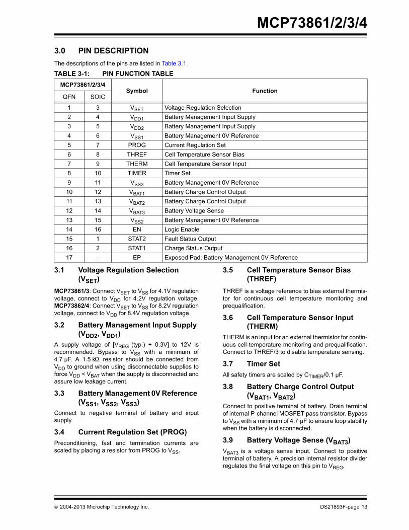
3.0 PIN DESCRIPTIONThe descriptions of the pins are listed in Table 3.1.
3.1 Voltage Regulation Selection (VSET)
MCP73861/3: Connect VSET to VSS for 4.1V regulationvoltage, connect to VDD for 4.2V regulation voltage.MCP73862/4: Connect VSET to VSS for 8.2V regulationvoltage, connect to VDD for 8.4V regulation voltage.
3.2 Battery Management Input Supply (VDD2, VDD1)
A supply voltage of [VREG (typ.) + 0.3V] to 12V isrecommended. Bypass to VSS with a minimum of4.7 µF. A 1.5 kΩ resistor should be connected fromVDD to ground when using disconnectable supplies toforce VDD < VBAT when the supply is disconnected andassure low leakage current.
3.3 Battery Management 0V Reference (VSS1, VSS2, VSS3)
Connect to negative terminal of battery and inputsupply.
3.4 Current Regulation Set (PROG)Preconditioning, fast and termination currents arescaled by placing a resistor from PROG to VSS.
3.5 Cell Temperature Sensor Bias (THREF)
THREF is a voltage reference to bias external thermis-tor for continuous cell temperature monitoring andprequalification.
3.6 Cell Temperature Sensor Input (THERM)
THERM is an input for an external thermistor for contin-uous cell-temperature monitoring and prequalification.Connect to THREF/3 to disable temperature sensing.
3.7 Timer SetAll safety timers are scaled by CTIMER/0.1 µF.
3.8 Battery Charge Control Output (VBAT1, VBAT2)
Connect to positive terminal of battery. Drain terminalof internal P-channel MOSFET pass transistor. Bypassto VSS with a minimum of 4.7 µF to ensure loop stabilitywhen the battery is disconnected.
3.9 Battery Voltage Sense (VBAT3)VBAT3 is a voltage sense input. Connect to positiveterminal of battery. A precision internal resistor dividerregulates the final voltage on this pin to VREG.
TABLE 3-1: PIN FUNCTION TABLEMCP73861/2/3/4
Symbol FunctionQFN SOIC
1 3 VSET Voltage Regulation Selection2 4 VDD1 Battery Management Input Supply3 5 VDD2 Battery Management Input Supply4 6 VSS1 Battery Management 0V Reference5 7 PROG Current Regulation Set6 8 THREF Cell Temperature Sensor Bias7 9 THERM Cell Temperature Sensor Input8 10 TIMER Timer Set9 11 VSS3 Battery Management 0V Reference
10 12 VBAT1 Battery Charge Control Output11 13 VBAT2 Battery Charge Control Output12 14 VBAT3 Battery Voltage Sense13 15 VSS2 Battery Management 0V Reference14 16 EN Logic Enable15 1 STAT2 Fault Status Output16 2 STAT1 Charge Status Output17 – EP Exposed Pad; Battery Management 0V Reference
2004-2013 Microchip Technology Inc. DS21893F-page 13

MCP73861/2/3/4
3.10 Logic Enable (EN)EN is an input to force charge termination, initiatecharge, clear faults or disable automatic recharge.3.11 Fault Status Output (STAT2)STAT2 is a current-limited, open-drain drive for directconnection to a LED for charge status indication. Alter-natively, a pull-up resistor can be applied for interfacingto a host microcontroller.
3.12 Charge Status Output (STAT1)STAT1 is a current-limited, open-drain drive for directconnection to a LED for charge status indication. Alter-natively, a pull-up resistor can be applied for interfacingto a host microcontroller.
3.13 Exposed Pad (EP)There is an internal electrical connection between theexposed thermal pad and VSS. The EP must beconnected to the same potential as the VSS pin on thePrinted Circuit Board (PCB).
DS21893F-page 14 2004-2013 Microchip Technology Inc.

MCP73861/2/3/4
4.0 DEVICE OVERVIEWThe MCP7386X family of devices are highly advancedlinear charge management controllers. Refer to thefunctional block diagram. Figure 4-2 depicts the opera-tional flow algorithm from charge initiation tocompletion and automatic recharge.
4.1 Charge Qualification and Preconditioning
Upon insertion of a battery, or application of an externalsupply, the MCP7386X family of devices automaticallyperforms a series of safety checks to qualify thecharge. The input source voltage must be above theUndervoltage Lockout (UVLO) threshold, the enablepin must be above the logic-high level and the celltemperature must be within the upper and lower thresh-olds. The qualification parameters are continuouslymonitored. Deviation beyond the limits automaticallysuspends or terminates the charge cycle. The inputvoltage must deviate below the UVLO stop thresholdfor at least one clock period to be considered valid.
Once the qualification parameters have been met, theMCP7386X initiates a charge cycle. The charge statusoutput is pulled low throughout the charge cycle (seeTable 5-1 for charge status outputs). If the batteryvoltage is below the preconditioning threshold (VPTH),the MCP7386X preconditions the battery with atrickle-charge. The preconditioning current is set toapproximately 10% of the fast charge regulationcurrent. The preconditioning trickle-charge safelyreplenishes deeply depleted cells and minimizes heatdissipation during the initial charge cycle. If the batteryvoltage has not exceeded the preconditioning thresh-old before the preconditioning timer has expired, a faultis indicated and the charge cycle is terminated.
4.2 Constant Current Regulation – Fast Charge
Preconditioning ends, and fast charging begins, whenthe battery voltage exceeds the preconditioningthreshold. Fast charge regulates to a constant current(IREG), which is set via an external resistor connectedto the PROG pin. Fast charge continues until thebattery voltage reaches the regulation voltage (VREG),or the fast charge timer expires; in which case, a faultis indicated and the charge cycle is terminated.
4.3 Constant Voltage RegulationWhen the battery voltage reaches the regulationvoltage (VREG), constant voltage regulation begins.The MCP7386X monitors the battery voltage at theVBAT pin. This input is tied directly to the positiveterminal of the battery.
The MCP7386X selects the voltage regulation valuebased on the state of VSET. With VSET tied to VSS, theMCP73861/3 and MCP73862/4 regulate to 4.1V and8.2V, respectively. With VSET tied to VDD, theMCP73861/3 and MCP73862/4 regulate to 4.2V and8.4V, respectively.
4.4 Charge Cycle Completion and Automatic Re-Charge
The MCP7386X monitors the charging current duringthe Constant-voltage regulation mode. The chargecycle is considered complete when the charge currenthas diminished below approximately 8% of theregulation current (IREG), or the elapsed timer hasexpired.
The MCP7386X automatically begins a new chargecycle when the battery voltage falls below the rechargethreshold (VRTH), assuming all the qualificationparameters are met.
4.5 Thermal RegulationThe MCP7386X family limits the charge current basedon the die temperature. Thermal regulation optimizesthe charge cycle time while maintaining device reliabil-ity. If thermal regulation is entered, the timer is automat-ically slowed down to ensure that a charge cycle willnot terminate prematurely. Figure 4-1 depicts thethermal regulation profile.
FIGURE 4-1: Typical Maximum Charge Current vs. Die Temperature.
4.6 Thermal ShutdownThe MCP7386X family suspends charge if the dietemperature exceeds 155°C. Charging will resumewhen the die temperature has cooled by approximately10°C. The thermal shutdown is a secondary safetyfeature in the event that there is a failure within thethermal regulation circuitry.
0
200
400
600
800
1000
1200
1400
0 20 40 60 80 100 120 140
Die Temperature (° C)
Max
imum
Cha
rge
Cur
rent
(mA
)
Minimum Maximum
2004-2013 Microchip Technology Inc. DS21893F-page 15

MCP73861/2/3/4
FIGURE 4-2: Operational Flow Algorithm.
Pre
cond
ition
ing
Mod
eC
harg
e C
urre
nt =
I PR
EG
Res
et S
afet
y Ti
mer
Yes
Initi
aliz
e
No
Yes
VB
AT >
VP
THS
TAT1
= O
n
VB
AT >
VP
TH
Yes
VD
D <
VU
VLO
No
No
Saf
ety
Tim
er
Yes
Tem
pera
ture
OK
No
STAT
1 =
Off
Safe
ty T
imer
Sus
pend
edC
harg
e C
urre
nt =
0
Faul
tC
harg
e C
urre
nt =
0R
eset
Saf
ety
Tim
er
or E
N L
owN
oS
TAT1
= O
ff
Con
stan
t-Cur
rent
Mod
e C
harg
e C
urre
nt =
I RE
GR
eset
Saf
ety
Tim
er
VB
AT =
VR
EG
No
No
Saf
ety
Tim
er
Yes
Tem
pera
ture
OK
Con
stan
t-Vol
tage
Mod
eO
utpu
t Vol
tage
= V
RE
G
I OU
T <
I TE
RM
Yes
VB
AT <
VR
TH
Ela
psed
Tim
er
Cha
rge
Term
inat
ion
Cha
rge
Cur
rent
= 0
Res
et S
afet
y Ti
mer N
oS
TAT1
= F
lash
ing
Yes
Yes
Tem
pera
ture
OK
No
STA
T1 =
Fla
shin
gS
afet
y Ti
mer
Sus
pend
edC
harg
e C
urre
nt =
0
Yes
Yes
VD
D <
VU
VLO
or E
N L
ow
No
Yes
Yes
Tem
pera
ture
OK
No
STAT
1 =
Off
Cha
rge
Cur
rent
= 0
Yes
No
STA
T1 =
Off
V DD
> V
UV
LO
Exp
ired
Exp
ired
No
STA
T1 =
Off
Saf
ety
Tim
er S
uspe
nded
Cha
rge
Cur
rent
= 0
EN
Hig
h
Expi
red
Not
e 1:
The
qual
ifica
tion
para
met
ers
are
cont
inuo
usly
mon
itore
d th
roug
hout
the
char
ge c
ycle
. Ref
er to
Sect
ion
4.1,
“C
harg
e Q
ualif
icat
ion
and
Prec
ondi
tioni
ng”,
for d
etai
ls.
Not
e 2:
The
char
ge c
urre
nt w
ill be
sca
led
base
d on
the
die
tem
pera
ture
dur
ing
ther
mal
regu
latio
n. R
efer
to
Sect
ion
4.5,
“T
herm
al
Reg
ulat
ion”
, fo
rde
tails
.
Not
e 1
Not
e 1
STA
T2 =
On
STAT
2 =
Flas
hing
STA
T2 =
Off
STAT
2 =
Flas
hing
STA
T2 =
Off
Not
e 2
STA
T2 =
Fla
shin
g
STA
T1 =
Off
(MC
P738
63/4
)
(MC
P738
61/2
)
STA
T2 =
Off
(All
Dev
ices
)
DS21893F-page 16 2004-2013 Microchip Technology Inc.

MCP73861/2/3/4
5.0 DETAILED DESCRIPTION
5.1 Analog Circuitry
5.1.1 BATTERY MANAGEMENT INPUT SUPPLY (VDD1, VDD2)
The VDD input is the input supply to the MCP7386X.The MCP7386X automatically enters a Power-downmode if the voltage on the VDD input falls below theUVLO voltage (VSTOP). This feature prevents drainingthe battery pack when the VDD supply is not present.The VDD inputs should be tied to ground with a resistor<= 1.5 kΩ to prevent VDD from floating and staying atVBAT level if the input supply is disconnected. Theresistor will assure that VDD < VBAT when the inputsupply is removed.
5.1.2 PROG INPUTFast charge current regulation can be scaled by placinga programming resistor (RPROG) from the PROG inputto VSS. Connecting the PROG input to VSS allows for amaximum fast charge current of 1.2A, typically. Theminimum fast charge current is 100 mA, set by lettingthe PROG input float. The following formula calculatesthe value for RPROG:
The preconditioning trickle-charge current and thecharge termination current are scaled to approximately10% and 8% of IREG, respectively.
5.1.3 CELL TEMPERATURE SENSOR BIAS (THREF)
A 2.5V voltage reference is provided to bias an externalthermistor for continuous cell temperature monitoringand prequalification. A ratio metric window comparisonis performed at threshold levels of VTHREF/2 andVTHREF/4.
5.1.4 CELL TEMPERATURE SENSOR INPUT (THERM)
The MCP73861/2/3/4 continuously monitors tempera-ture by comparing the voltage between the THERMinput and VSS with the upper and lower temperaturethresholds. A negative or positive temperature coeffi-cient, NTC or PTC thermistor and an external voltage-divider typically develop this voltage. The temperaturesensing circuit has its own reference to which itperforms a ratio metric comparison. Therefore, it isimmune to fluctuations in the supply input (VDD). The
temperature-sensing circuit is removed from thesystem when VDD is not applied, eliminating additionaldischarge of the battery pack.
Figure 6-1 depicts a typical application circuit withconnection of the THERM input. The resistor values ofRT1 and RT2 are calculated with the followingequations.
For NTC thermistors:
For PTC thermistors:
Applying a voltage equal to VTHREF/3 to the THERMinput disables temperature monitoring.
5.1.5 TIMER SET INPUT (TIMER)The TIMER input programs the period of the safetytimers by placing a timing capacitor (CTIMER) betweenthe TIMER input pin and VSS. Three safety timers areprogrammed via the timing capacitor.
The preconditioning safety timer period:
The fast charge safety timer period:
The elapsed time termination period:
The preconditioning timer starts after qualification andresets when the charge cycle transitions to the fastcharge, Constant-current mode. The fast charge timerand the elapsed timer start once the MCP7386Xtransitions from preconditioning. The fast charge timerresets when the charge cycle transitions to theConstant-voltage mode. The elapsed timer will expireand terminate the charge if the sensed current does notdiminish below the termination threshold.
RPROG13.2 11 IREG–
12 IREG 1.2–----------------------------------------=
Where:
IREG = the desired fast charge current in amps.RPROG = measured in kΩ
RT12 RCOLD RHOTRCOLD RHOT–
----------------------------------------------=
RT22 RCOLD RHOTRCOLD 3 R HOT–----------------------------------------------=
RT12 RCOLD RHOTRHOT RCOLD–
----------------------------------------------=
RT22 RCOLD RHOTRHOT 3 R COLD–----------------------------------------------=
Where:
RCOLD and RHOT are the thermistor resis-tance values at the temperature window ofinterest.
tPRECONCTIMER0.1F------------------- 1.0Hour s=
tFASTCTIMER0.1F------------------- 1.5Hours=
tTERMCTIMER0.1F------------------- 3.0Hours=
2004-2013 Microchip Technology Inc. DS21893F-page 17

MCP73861/2/3/4
During thermal regulation, the timer is slowed downproportional to the charge current.5.1.6 BATTERY VOLTAGE SENSE (VBAT3)The MCP7386X monitors the battery voltage at theVBAT3 pin. This input is tied directly to the positiveterminal of the battery pack.
5.1.7 BATTERY CHARGE CONTROL OUTPUT (VBAT1, VBAT2)
The battery charge control output is the drain terminalof an internal P-channel MOSFET. The MCP7386Xprovides constant current and voltage regulation to thebattery pack by controlling this MOSFET in the linearregion. The battery charge control output should beconnected to the positive terminal of the battery pack.
5.2 Digital Circuitry
5.2.1 CHARGE STATUS OUTPUTS (STAT1, STAT2)
Two status outputs provide information on the state ofcharge. The current-limited, open-drain outputs can beused to illuminate external LEDs. Optionally, a pull-upresistor can be used on the output for communicationwith a host microcontroller. Table 5-1 summarizes thestate of the status outputs during a charge cycle.
The flashing rate (1 Hz) is based off a timer capacitor(CTIMER) of 0.1 µF. The rate will vary based on thevalue of the timer capacitor.
During a Fault condition, the STAT1 status output willbe off and the STAT2 status output will be on. Torecover from a Fault condition, the input voltage mustbe removed and then reapplied, or the enable input(EN) must be de-asserted to a logic-low, then assertedto a logic-high.
When the voltage on the THERM input is outside thepreset window, the charge cycle will not start, or will besuspended. The charge cycle is not terminated andrecovery is automatic. The charge cycle will resume (orstart) once the THERM input is valid and all otherqualification parameters are met. During an invalidTHERM condition, the STAT1 status output will be offand the STAT2 status output will flash.
5.2.2 VSET INPUTThe VSET input selects the regulated output voltage ofthe MCP7386X. With VSET tied to VSS, the MCP73861/3 and MCP73862/4 regulate to 4.1V and 8.2V, respec-tively. With VSET tied to VDD, the MCP73861/3 andMCP73862/4 regulate to 4.2V and 8.4V, respectively.
5.2.3 LOGIC ENABLE (EN)The logic enable input pin (EN) can be used to termi-nate a charge at any time during the charge cycle, aswell as to initiate a charge cycle or initiate a rechargecycle.
Applying a logic-high input signal to the EN pin, or tyingit to the input source, enables the device. Applying alogic-low input signal disables the device and termi-nates a charge cycle. When disabled, the device’ssupply current is reduced to 0.17 µA, typically.
TABLE 5-1: STATUS OUTPUTSCHARGE
CYCLE STAT1 STAT1 STAT2
Qualification Off OffPreconditioning On OffConstant-Current Fast Charge
On Off
Constant-Voltage On OffCharge Complete Flashing (1 Hz,
50% duty cycle)(MCP73861/2) Off
(All Devices)Off
(MCP73863/4)Fault Off OnTHERM Invalid Off Flashing (1 Hz
50% duty cycle)Disabled – Sleep mode
Off Off
Input Voltage Dis-connected (1.5KΩ Pulldown)
Off Off
Legend: Off state: Open-drain is high-impedanceOn state: Open-drain can sink current
typically 7 mAFlashing: Toggles between off state and
on state
DS21893F-page 18 2004-2013 Microchip Technology Inc.

MCP73861/2/3/4
6.0 APPLICATIONSThe MCP7386X is designed to operate in conjunctionwith a host microcontroller or in stand-alone applica-tions. The MCP7386X provides the preferred chargealgorithm for Lithium-Ion and Lithium-Polymer cellsConstant-current followed by Constant-voltage.
Figure 6-1 illustrates a typical stand-alone applicationcircuit, while Figures 6-2 and 6-3 illustrate theaccompanying charge profile
.
FIGURE 6-1: Typical Application Circuit.
FIGURE 6-2: Typical Charge Profile.
ENSTAT1 STA
T2
VSET
VSS3
VDD1
VDD2
VSS2
TIMERPROGTH
ER
M
THR
EF
VBAT3
VBAT2
VBAT1
CTIMER
Unregulated Wall Cube
RPROG
RT1
RT2
+–
Single Lithium-IonCell
VSS1
1
2
3
4
MCP73861
141516
5 6 7 89
10
11
1213
1.5K
RegulationVoltage (VREG)
RegulationCurrent (IREG)
TransitionThreshold(VPTH)
PreconditionCurrent (IPREG)
Precondition Safety Timer
Fast Charge Safety Timer
Elapsed Time Termination Timer
Charge Voltage
Preconditioning Mode
Constant-Current Mode
Constant-VoltageMode
Charge Current
TerminationCurrent (ITERM)
2004-2013 Microchip Technology Inc. DS21893F-page 19

MCP73861/2/3/4
FIGURE 6-3: Typical Charge Profile in Thermal Regulation.
6.1 Application Circuit Design Due to the low efficiency of linear charging, the mostimportant factors are thermal design and cost, whichare a direct function of the input voltage, output currentand thermal impedance between the battery chargerand the ambient cooling air. The worst-case situation iswhen the device has transitioned from thePreconditioning mode to the Constant-current mode. Inthis situation, the battery charger has to dissipate themaximum power. A trade-off must be made betweenthe charge current, cost and thermal requirements ofthe charger.
6.1.1 COMPONENT SELECTIONSelection of the external components in Figure 6-1 iscrucial to the integrity and reliability of the chargingsystem. The following discussion is intended as a guidefor the component selection process.
6.1.1.1 Current Programming Resistor (RPROG)
The preferred fast charge current for Lithium-Ion cellsis at the 1C rate, with an absolute maximum current atthe 2C rate. For example, a 500 mAh battery pack hasa preferred fast charge current of 500 mA. Charging atthis rate provides the shortest charge cycle timeswithout degradation to the battery pack performance orlife.
1200 mA is the maximum charge current obtainablefrom the MCP7386X. For this situation, the PROG inputshould be connected directly to VSS.
6.1.1.2 Thermal ConsiderationsThe worst-case power dissipation in the batterycharger occurs when the input voltage is at themaximum and the device has transitioned from the Pre-conditioning mode to the Constant-current mode. Inthis case, the power dissipation is:
Regulation Voltage (VREG)Regulation Current (IREG)
Transition Threshold (VPTH)
Precondition Safety Timer
Fast Charge Safety Timer
Elapsed Time Termination Timer
Charge Voltage
Preconditioning Mode
Constant-Current Mode
Constant-Voltage Mode
Charge Current
Precondition Current (IPREG)Termination Current (ITERM)
PowerDissipation VDDMAX VPTHMIN– IREGMAX=
Where:
VDDMAX = the maximum input voltageIREGMAX = the maximum fast charge currentVPTHMIN = the minimum transition threshold
voltage
DS21893F-page 20 2004-2013 Microchip Technology Inc.

MCP73861/2/3/4
Power dissipation with a 5V, ±10% input voltage sourceis:With the battery charger mounted on a 1 in2 pad of1 oz. copper, the junction temperature rise is 60°C,approximately. This would allow for a maximum operat-ing ambient temperature of 50°C before thermalregulation is entered.
6.1.1.3 External CapacitorsThe MCP7386X is stable with or without a battery load.In order to maintain good AC stability in the Constant-voltage mode, a minimum capacitance of 4.7 µF isrecommended to bypass the VBAT pin to VSS. Thiscapacitance provides compensation when there is nobattery load. In addition, the battery and interconnec-tions appear inductive at high frequencies. Theseelements are in the control feedback loop duringConstant-voltage mode. Therefore, the bypasscapacitance may be necessary to compensate for theinductive nature of the battery pack.
Virtually any good quality output filter capacitor can beused, independent of the capacitor’s minimumEffective Series Resistance (ESR) value. The actualvalue of the capacitor (and its associated ESR)depends on the output load current. A 4.7 µF ceramic,tantalum or aluminum electrolytic capacitor at theoutput is usually sufficient to ensure stability for up to a1A output current.
6.1.1.4 Reverse-Blocking ProtectionThe MCP7386X provides protection from a faulted orshorted input, or from a reversed-polarity input source.Without the protection, a faulted or shorted input woulddischarge the battery pack through the body diode ofthe internal pass transistor.
6.1.1.5 Enable InterfaceIn the stand-alone configuration, the enable pin isgenerally tied to the input voltage. The MCP7386Xautomatically enters a Low-power mode when voltageon the VDD input falls below the UVLO voltage (VSTOP),reducing the battery drain current to 0.23 µA,typically.
6.1.1.6 Charge Status InterfaceTwo status outputs provide information on the state ofcharge. The current-limited, open-drain outputs can beused to illuminate external LEDs. Refer to Table 5-1 fora summary of the state of the status outputs during acharge cycle.
6.2 PCB Layout IssuesFor optimum voltage regulation, place the battery packas close as possible to the device’s VBAT and VSS pins,recommended to minimize voltage drops along thehigh current-carrying PCB traces.
If the PCB layout is used as a heatsink, adding manyvias in the heatsink pad can help conduct more heat tothe backplane of the PCB, thus reducing the maximumjunction temperature.
PowerDissipation 5.5V 2.7V– 575mA 1.61W= =
2004-2013 Microchip Technology Inc. DS21893F-page 21

MCP73861/2/3/4
NOTES:DS21893F-page 22 2004-2013 Microchip Technology Inc.

MCP73861/2/3/4
7.0 PACKAGING INFORMATION
7.1 Package Marking Information
16-Lead QFN Example:
16-Lead SOIC (150 mil) Example:
XXXXXXXXXXXXX
YYWWNNNXXXXXXXXXXXXX
MCP73861
1108256
Legend: XX...X Customer-specific informationY Year code (last digit of calendar year)YY Year code (last 2 digits of calendar year)WW Week code (week of January 1 is week ‘01’)NNN Alphanumeric traceability code Pb-free JEDEC designator for Matte Tin (Sn)* This package is Pb-free. The Pb-free JEDEC designator ( )
can be found on the outer packaging for this package.
Note: In the event the full Microchip part number cannot be marked on one line, it willbe carried over to the next line, thus limiting the number of availablecharacters for customer-specific information.
3e
3e
I/SL^ 3e
XXXXXXXXXXXXXXXXX
YWWNNN
73861I/ML1108256
2004-2013 Microchip Technology Inc. DS21893F-page 23

MCP73861/2/3/4
!""#$%&
' !"# $% &" ' ()"&'"!&) & #*&& & # + !!*!"& #, ' !#& -./
012 0!' ! & $& " !**&"&& !-32 % ' !("!"*&"&& (%%'&"! !
' 3& '!&" &+ #*!( ! ! & + %&& #&&&244***''4+
5&! 66--' !6'&! 7 78 9
7"') %! 7 :& :/018 ; & &#%% /1&&+ !! , -38 <#& - 01-$! ##<#& - / :/ 8 6 & 01-$! ##6 & / :/ 1&&<#& ) / , ,/1&&6 & 6 , /1&&&-$! ## = > >
D
E
N
2
1
EXPOSEDPAD
D2
E22
1
e
b
KN
NOTE 1
A3
A1
A
LTOP VIEW BOTTOM VIEW
* 10
DS21893F-page 24 2004-2013 Microchip Technology Inc.

MCP73861/2/3/4
Note: For the most current package drawings, please see the Microchip Packaging Specification located at http://www.microchip.com/packaging
2004-2013 Microchip Technology Inc. DS21893F-page 25

MCP73861/2/3/4
Note: For the most current package drawings, please see the Microchip Packaging Specification located at http://www.microchip.com/packaging
DS21893F-page 26 2004-2013 Microchip Technology Inc.

MCP73861/2/3/4
Note: For the most current package drawings, please see the Microchip Packaging Specification located at http://www.microchip.com/packaging
2004-2013 Microchip Technology Inc. DS21893F-page 27

MCP73861/2/3/4
Note: For the most current package drawings, please see the Microchip Packaging Specification located at http://www.microchip.com/packaging
DS21893F-page 28 2004-2013 Microchip Technology Inc.

MCP73861/2/3/4
APPENDIX A: REVISION HISTORY
Revision F (March 2013)The following is the list of modifications:
1. Added the Output Reverse Leakage SwitchoverTime parameter to the DC Characteristics table.
2. Updated Section 3.2.3. Updated Section 5.1.1.4. Updated Figure 6-1.
Revision E (April 2011)The following is the list of modifications:
1. Updated Figure 2-4.
Revision D (December 2008)The following is the list of modifications:
1. Updated package outline diagrams.
Revision C (August 2005)The following is the list of modifications:
1. Added MCP73863 and MCP73864 devicesthroughout data sheet.
2. Added Appendix A: Revision History.3. Updated QFN and SOIC package diagrams.
Revision B (December 2004)The following is the list of modifications:
Added SOIC package throughout data sheet.
Revision A (June 2004)Original Release of this Document.
2004-2013 Microchip Technology Inc. DS21893F-page 29

MCP73861/2/3/4
NOTES:DS21893F-page 30 2004-2013 Microchip Technology Inc.

MCP73861/2/3/4
PRODUCT IDENTIFICATION SYSTEMTo order or obtain information, e.g., on pricing or delivery, contact the Microchip sales office.
PART NO. X /XX
PackageTemperatureRange
Device
Device: MCP73861: Single-Cell Charge Controller with Temperature Monitor
MCP73861T: Single-Cell Charge Controller with Temperature Monitor, Tape and Reel
MCP73862: Dual Series Cells Charge Controller with Temperature Monitor
MCP73862T: Dual Series Cells Charge Controller with Temperature Monitor, Tape and Reel
MCP73863: Single-cell Charge Controller with Temperature Monitor
MCP73863T: Single-Cell Charge Controller with Temperature Monitor, Tape and Reel
MCP73864: Dual Series Cells Charge Controller with Temperature Monitor
MCP73864T: Dual Series Cells Charge Controller with Temperature Monitor, Tape and Reel
Temperature Range: I = -40C to +85C (Industrial)
Package: ML = Plastic Quad Flat No Lead, 4x4 mm Body (QFN),16-lead
SL = Plastic Small Outline, 150 mm Body (SOIC),16-lead
Examples:a) MCP73861-I/ML: Single-Cell Controller
16LD-QFN package.b) MCP73861T-I/ML: Tape and Reel,
Single-Cell Controller16LD-QFN package.
c) MCP73861-I/SL: Single-Cell Controller16LD-SOIC package.
d) MCP73861T-I/SL: Tape and Reel,Single-Cell Controller16LD-SOIC package.
a) MCP73862-I/ML: Dual-Cell Controller16LD-QFN package.
b) MCP73862T-I/ML: Tape and Reel,Dual-Cell Controller16LD-QFN package.
c) MCP73862-I/SL: Dual-Cell Controller16LD-SOIC package.
d) MCP73862T-I/SL: Tape and Reel,Dual-Cell Controller16LD-SOIC package.
a) MCP73863-I/ML: Single-Cell Controller16LD-QFN package.
b) MCP73863T-I/ML: Tape and Reel,Single-Cell Controller16LD-QFN package.
c) MCP73863-I/SL: Single-Cell Controller16LD-SOIC package.
d) MCP73863T-I/SL: Tape and Reel,Single-Cell Controller16LD-SOIC package.
a) MCP73864-I/ML: Dual-Cell Controller16LD-QFN package.
b) MCP73864T-I/ML: Tape and Reel,Dual-Cell Controller16LD-QFN package.
c) MCP73864-I/SL: Dual-Cell Controller16LD-SOIC package.
d) MCP73864T-I/SL: Tape and Reel,Dual-Cell Controller16LD-SOIC package.
2004-2013 Microchip Technology Inc. DS21893F-page 31

MCP73861/2/3/4
NOTES:DS21893F-page 32 2004-2013 Microchip Technology Inc.

Note the following details of the code protection feature on Microchip devices:• Microchip products meet the specification contained in their particular Microchip Data Sheet.
• Microchip believes that its family of products is one of the most secure families of its kind on the market today, when used in the intended manner and under normal conditions.
• There are dishonest and possibly illegal methods used to breach the code protection feature. All of these methods, to our knowledge, require using the Microchip products in a manner outside the operating specifications contained in Microchip’s Data Sheets. Most likely, the person doing so is engaged in theft of intellectual property.
• Microchip is willing to work with the customer who is concerned about the integrity of their code.
• Neither Microchip nor any other semiconductor manufacturer can guarantee the security of their code. Code protection does not mean that we are guaranteeing the product as “unbreakable.”
Code protection is constantly evolving. We at Microchip are committed to continuously improving the code protection features of ourproducts. Attempts to break Microchip’s code protection feature may be a violation of the Digital Millennium Copyright Act. If such actsallow unauthorized access to your software or other copyrighted work, you may have a right to sue for relief under that Act.
Information contained in this publication regarding deviceapplications and the like is provided only for your convenienceand may be superseded by updates. It is your responsibility toensure that your application meets with your specifications.MICROCHIP MAKES NO REPRESENTATIONS ORWARRANTIES OF ANY KIND WHETHER EXPRESS ORIMPLIED, WRITTEN OR ORAL, STATUTORY OROTHERWISE, RELATED TO THE INFORMATION,INCLUDING BUT NOT LIMITED TO ITS CONDITION,QUALITY, PERFORMANCE, MERCHANTABILITY ORFITNESS FOR PURPOSE. Microchip disclaims all liabilityarising from this information and its use. Use of Microchipdevices in life support and/or safety applications is entirely atthe buyer’s risk, and the buyer agrees to defend, indemnify andhold harmless Microchip from any and all damages, claims,suits, or expenses resulting from such use. No licenses areconveyed, implicitly or otherwise, under any Microchipintellectual property rights.
2004-2013 Microchip Technology Inc.
QUALITY MANAGEMENT SYSTEM CERTIFIED BY DNV
== ISO/TS 16949 ==
Trademarks
The Microchip name and logo, the Microchip logo, dsPIC, FlashFlex, KEELOQ, KEELOQ logo, MPLAB, PIC, PICmicro, PICSTART, PIC32 logo, rfPIC, SST, SST Logo, SuperFlash and UNI/O are registered trademarks of Microchip Technology Incorporated in the U.S.A. and other countries.
FilterLab, Hampshire, HI-TECH C, Linear Active Thermistor, MTP, SEEVAL and The Embedded Control Solutions Company are registered trademarks of Microchip Technology Incorporated in the U.S.A.
Silicon Storage Technology is a registered trademark of Microchip Technology Inc. in other countries.
Analog-for-the-Digital Age, Application Maestro, BodyCom, chipKIT, chipKIT logo, CodeGuard, dsPICDEM, dsPICDEM.net, dsPICworks, dsSPEAK, ECAN, ECONOMONITOR, FanSense, HI-TIDE, In-Circuit Serial Programming, ICSP, Mindi, MiWi, MPASM, MPF, MPLAB Certified logo, MPLIB, MPLINK, mTouch, Omniscient Code Generation, PICC, PICC-18, PICDEM, PICDEM.net, PICkit, PICtail, REAL ICE, rfLAB, Select Mode, SQI, Serial Quad I/O, Total Endurance, TSHARC, UniWinDriver, WiperLock, ZENA and Z-Scale are trademarks of Microchip Technology Incorporated in the U.S.A. and other countries.
SQTP is a service mark of Microchip Technology Incorporated in the U.S.A.
GestIC and ULPP are registered trademarks of Microchip Technology Germany II GmbH & Co. KG, a subsidiary of Microchip Technology Inc., in other countries.
All other trademarks mentioned herein are property of their respective companies.
© 2004-2013, Microchip Technology Incorporated, Printed in the U.S.A., All Rights Reserved.
Printed on recycled paper.
ISBN: 9781620770405
Microchip received ISO/TS-16949:2009 certification for its worldwide
DS21893F-page 33
headquarters, design and wafer fabrication facilities in Chandler and Tempe, Arizona; Gresham, Oregon and design centers in California and India. The Company’s quality system processes and procedures are for its PIC® MCUs and dsPIC® DSCs, KEELOQ® code hopping devices, Serial EEPROMs, microperipherals, nonvolatile memory and analog products. In addition, Microchip’s quality system for the design and manufacture of development systems is ISO 9001:2000 certified.

DS21893F-page 34 2004-2013 Microchip Technology Inc.
AMERICASCorporate Office2355 West Chandler Blvd.Chandler, AZ 85224-6199Tel: 480-792-7200 Fax: 480-792-7277Technical Support: http://www.microchip.com/supportWeb Address: www.microchip.comAtlantaDuluth, GA Tel: 678-957-9614 Fax: 678-957-1455BostonWestborough, MA Tel: 774-760-0087 Fax: 774-760-0088ChicagoItasca, IL Tel: 630-285-0071 Fax: 630-285-0075ClevelandIndependence, OH Tel: 216-447-0464 Fax: 216-447-0643DallasAddison, TX Tel: 972-818-7423 Fax: 972-818-2924DetroitFarmington Hills, MI Tel: 248-538-2250Fax: 248-538-2260IndianapolisNoblesville, IN Tel: 317-773-8323Fax: 317-773-5453Los AngelesMission Viejo, CA Tel: 949-462-9523 Fax: 949-462-9608Santa ClaraSanta Clara, CA Tel: 408-961-6444Fax: 408-961-6445TorontoMississauga, Ontario, CanadaTel: 905-673-0699 Fax: 905-673-6509
ASIA/PACIFICAsia Pacific OfficeSuites 3707-14, 37th FloorTower 6, The GatewayHarbour City, KowloonHong KongTel: 852-2401-1200Fax: 852-2401-3431Australia - SydneyTel: 61-2-9868-6733Fax: 61-2-9868-6755China - BeijingTel: 86-10-8569-7000 Fax: 86-10-8528-2104China - ChengduTel: 86-28-8665-5511Fax: 86-28-8665-7889China - ChongqingTel: 86-23-8980-9588Fax: 86-23-8980-9500China - HangzhouTel: 86-571-2819-3187 Fax: 86-571-2819-3189China - Hong Kong SARTel: 852-2943-5100 Fax: 852-2401-3431China - NanjingTel: 86-25-8473-2460Fax: 86-25-8473-2470China - QingdaoTel: 86-532-8502-7355Fax: 86-532-8502-7205China - ShanghaiTel: 86-21-5407-5533 Fax: 86-21-5407-5066China - ShenyangTel: 86-24-2334-2829Fax: 86-24-2334-2393China - ShenzhenTel: 86-755-8864-2200 Fax: 86-755-8203-1760China - WuhanTel: 86-27-5980-5300Fax: 86-27-5980-5118China - XianTel: 86-29-8833-7252Fax: 86-29-8833-7256China - XiamenTel: 86-592-2388138 Fax: 86-592-2388130China - ZhuhaiTel: 86-756-3210040 Fax: 86-756-3210049
ASIA/PACIFICIndia - BangaloreTel: 91-80-3090-4444 Fax: 91-80-3090-4123India - New DelhiTel: 91-11-4160-8631Fax: 91-11-4160-8632India - PuneTel: 91-20-2566-1512Fax: 91-20-2566-1513Japan - OsakaTel: 81-6-6152-7160 Fax: 81-6-6152-9310Japan - TokyoTel: 81-3-6880- 3770 Fax: 81-3-6880-3771Korea - DaeguTel: 82-53-744-4301Fax: 82-53-744-4302Korea - SeoulTel: 82-2-554-7200Fax: 82-2-558-5932 or 82-2-558-5934Malaysia - Kuala LumpurTel: 60-3-6201-9857Fax: 60-3-6201-9859Malaysia - PenangTel: 60-4-227-8870Fax: 60-4-227-4068Philippines - ManilaTel: 63-2-634-9065Fax: 63-2-634-9069SingaporeTel: 65-6334-8870Fax: 65-6334-8850Taiwan - Hsin ChuTel: 886-3-5778-366Fax: 886-3-5770-955Taiwan - KaohsiungTel: 886-7-213-7828Fax: 886-7-330-9305Taiwan - TaipeiTel: 886-2-2508-8600 Fax: 886-2-2508-0102Thailand - BangkokTel: 66-2-694-1351Fax: 66-2-694-1350
EUROPEAustria - WelsTel: 43-7242-2244-39Fax: 43-7242-2244-393Denmark - CopenhagenTel: 45-4450-2828 Fax: 45-4485-2829France - ParisTel: 33-1-69-53-63-20 Fax: 33-1-69-30-90-79Germany - MunichTel: 49-89-627-144-0 Fax: 49-89-627-144-44Italy - Milan Tel: 39-0331-742611 Fax: 39-0331-466781Netherlands - DrunenTel: 31-416-690399 Fax: 31-416-690340Spain - MadridTel: 34-91-708-08-90Fax: 34-91-708-08-91UK - WokinghamTel: 44-118-921-5869Fax: 44-118-921-5820
Worldwide Sales and Service
11/29/12