mcp4021/2/3/4 low-cost nv digital pot with wiperlock … · 2018. 2. 1. · -0.5 0 +0.5 lsb 2.7v...
TRANSCRIPT
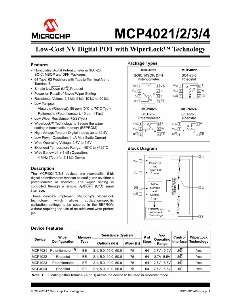
MCP4021/2/3/4Low-Cost NV Digital POT with WiperLock™ Technology
Features• Nonvolatile Digital Potentiometer in SOT-23,
SOIC, MSOP and DFN Packages
• 64 Taps: 63 Resistors with Taps to Terminal A and Terminal B
• Simple Up/Down (U/D) Protocol
• Power-on Recall of Saved Wiper Setting
• Resistance Values: 2.1 k, 5 k, 10 k or 50 k• Low Tempco:
- Absolute (Rheostat): 50 ppm (0°C to 70°C Typ.)
- Ratiometric (Potentiometer): 10 ppm (Typ.)
• Low Wiper Resistance: 75 (Typ.)
• WiperLock™ Technology to Secure the wiper setting in nonvolatile memory (EEPROM)
• High-Voltage Tolerant Digital Inputs: up to 12.5V
• Low-Power Operation: 1 µA Max Static Current
• Wide Operating Voltage: 2.7V to 5.5V
• Extended Temperature Range: –40°C to +125°C
• Wide Bandwidth (-3 dB) Operation:
- 4 MHz (Typ.) for 2.1 k Device
DescriptionThe MCP4021/2/3/4 devices are nonvolatile, 6-bitdigital potentiometers that can be configured as either apotentiometer or rheostat. The wiper setting iscontrolled through a simple Up/Down (U/D) serialinterface.
These device’s implement Microchip’s WiperLocktechnology, which allows application-specificcalibration settings to be secured in the EEPROMwithout requiring the use of an additional write-protectpin.
Package Types
Block Diagram
Device Features
.
A
W
B
MCP4021
SOIC, MSOP, DFN
MCP4022
SOT-23-6
MCP4023
SOT-23-6
MCP4024
SOT-23-5
RheostatPotentiometer
Potentiometer Rheostat
A
VSS
W
1
2
3
4
8
7
6
5
VDD U/D
NC
B
CS
4
1
2
3
5 W
CS
VDD
VSS
U/D
4
1
2
3
6 A
CS
VDD
VSS
U/D
5 WA
W
B
4
1
2
3
6 A
CS
VDD
VSS
U/D
5 W
A
W
W
AB B
VDD
VSS
U/D
W
B
(Re
sist
or
Arr
ay)
Wip
er
Re
gis
ter
CS
WiperLockEEPROM and
A
2-WireInterface
andControlLogic
Power-Upand
Brown-OutControl
Technology
DeviceWiper
ConfigurationMemory
Type
Resistance (typical)# of
Steps
VDD Operating
Range
Control Interface
WiperLock TechnologyOptions (k) Wiper ()
MCP4021 Potentiometer (1) EE 2.1, 5.0, 10.0, 50.0 75 64 2.7V - 5.5V U/D Yes
MCP4022 Rheostat EE 2.1, 5.0, 10.0, 50.0 75 64 2.7V- 5.5V U/D Yes
MCP4023 Potentiometer EE 2.1, 5.0, 10.0, 50.0 75 64 2.7V - 5.5V U/D Yes
MCP4024 Rheostat EE 2.1, 5.0, 10.0, 50.0 75 64 2.7V - 5.5V U/D Yes
Note 1: Floating either terminal (A or B) allows the device to be used in Rheostat mode.
2006-2017 Microchip Technology Inc. DS20001945F-page 1
MCP4021/2/3/4
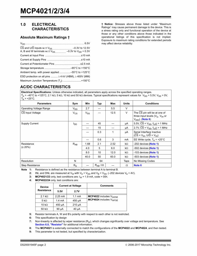
1.0 ELECTRICAL CHARACTERISTICS
Absolute Maximum Ratings †
VDD............................................................................................................. 6.5V
CS and U/D inputs w.r.t VSS................................... –0.3V to 12.5VA, B and W terminals w.r.t VSS................... –0.3V to VDD + 0.3V
Current at Input Pins ..................................................±10 mA
Current at Supply Pins ...............................................±10 mA
Current at Potentiometer Pins ...................................±2.5 mA
Storage temperature ....................................–65°C to +150°C
Ambient temp. with power applied ...............–55°C to +125°C
ESD protection on all pins 4 kV (HBM), 400V (MM)
Maximum Junction Temperature (TJ) . .........................+150°C
† Notice: Stresses above those listed under “MaximumRatings” may cause permanent damage to the device. This isa stress rating only and functional operation of the device atthose or any other conditions above those indicated in theoperational listings of this specification is not implied.Exposure to maximum rating conditions for extended periodsmay affect device reliability.
AC/DC CHARACTERISTICSElectrical Specifications: Unless otherwise indicated, all parameters apply across the specified operating ranges.TA = –40°C to +125°C, 2.1 k5 k10 kand50 kdevicesTypical specifications represent values for VDD = 5.5V, VSS = 0V,TA = +25°C.
Parameters Sym Min Typ Max Units Conditions
Operating Voltage Range VDD 2.7 — 5.5 V
CS Input Voltage VCS VSS — 12.5 V The CS pin will be at one of three input levels (VIL, VIH or VIHH). (Note 6)
Supply Current IDD — 45 — µA 5.5V, CS = VSS, fU/D = 1 MHz
— 15 — µA 2.7V, CS = VSS, fU/D = 1 MHz
— 0.3 1 µA Serial Interface Inactive(CS = VIH, U/D = VIH)
— 0.6 3 mA EE Write cycle, TA = +25°C
Resistance(± 20%)
RAB 1.68 2.1 2.52 k -202 devices(Note 1)
4.0 5 6.0 k -502 devices(Note 1)
8.0 10 12.0 k -103 devices(Note 1)
40.0 50 60.0 k -503 devices(Note 1)
Resolution N 64 Taps No Missing Codes
Step Resistance RS — RAB / 63 — Note 6
Note 1: Resistance is defined as the resistance between terminal A to terminal B.2: INL and DNL are measured at VW with VA = VDD and VB = VSS. (–202 devices VA = 4V).3: MCP4021/23 only, test conditions are: IW = 1.9 mA, code = 00h.4: MCP4022/24 only, test conditions are:
5: Resistor terminals A, W and B’s polarity with respect to each other is not restricted.6: This specification by design7: Non-linearity is affected by wiper resistance (RW), which changes significantly over voltage and temperature. See
Section 6.0, "Resistor" for additional information.8: The MCP4021 is externally connected to match the configurations of the MCP4022 and MCP4024, and then tested.9: This parameter is not tested, but specified by characterization.
Device Resistance
Current at Voltage Comments
5.5V 2.7V
2.1 k 2.25 mA 1.1 mA MCP4022 includes VWZSE MCP4024 includes VWFSE 5 k 1.4 mA 450 µA
10 k 450 µA 210 µA
50 k 90 µA 40 µA
DS20001945F-page 2 2006-2017 Microchip Technology Inc.

MCP4021/2/3/4
Wiper Resistance (Note 3, Note 4) RW — 70 125 5.5V
— 70 325 2.7V
Nominal Resistance Tempco R/T — 50 — ppm/°C TA = –20°C to +70°C
— 100 — ppm/°C TA = –40°C to +85°C
— 150 — ppm/°C TA = –40°C to +125°C
Ratiometeric Tempco VWA/T — 10 — ppm/°C MCP4021 and MCP4023 only,code = 1Fh
Full-Scale Error VWFSE -0.5 -0.1 +0.5 LSb Code 3Fh (MCP4021/23 only)
Zero-Scale Error VWZSE -0.5 +0.1 +0.5 LSb Code 00h (MCP4021/23 only)
Monotonicity N Yes Bits
Potentiometer Integral Non-linearity INL -0.5 ±0.25 +0.5 LSb MCP4021/23 only (Note 2)
Potentiometer DifferentialNonlinearity
DNL -0.5 ±0.25 +0.5 LSb MCP4021/23 only (Note 2)
Resistor Terminal Input Voltage Range (Terminals A, B and W)
VA,VW,VB Vss — VDD V Note 5, Note 6
Maximum current through A, W or B IW — — 2.5 mA Note 6
Leakage current into A, W or B IWL — 100 — nA MCP4021 A = W = B = VSS
— 100 — nA MCP4022/23 A = W = VSS
— 100 — nA MCP4024 W = VSS
Capacitance (PA) CAW — 75 — pF f =1 MHz, code = 1Fh
Capacitance (Pw) CW — 120 — pF f =1 MHz, code = 1Fh
Capacitance (PB) CBW — 75 — pF f =1 MHz, code = 1Fh
Bandwidth -3 dB BW — 4 — MHz -202 devices
Code = 1F,output load = 30 pF
— 2 — MHz -502 devices
— 1 — MHz -103 devices
— 200 — kHz -503 devices
AC/DC CHARACTERISTICS (CONTINUED)Electrical Specifications: Unless otherwise indicated, all parameters apply across the specified operating ranges.TA = –40°C to +125°C, 2.1 k5 k10 kand50 kdevicesTypical specifications represent values for VDD = 5.5V, VSS = 0V,TA = +25°C.
Parameters Sym Min Typ Max Units Conditions
Note 1: Resistance is defined as the resistance between terminal A to terminal B.2: INL and DNL are measured at VW with VA = VDD and VB = VSS. (–202 devices VA = 4V).3: MCP4021/23 only, test conditions are: IW = 1.9 mA, code = 00h.4: MCP4022/24 only, test conditions are:
5: Resistor terminals A, W and B’s polarity with respect to each other is not restricted.6: This specification by design7: Non-linearity is affected by wiper resistance (RW), which changes significantly over voltage and temperature. See
Section 6.0, "Resistor" for additional information.8: The MCP4021 is externally connected to match the configurations of the MCP4022 and MCP4024, and then tested.9: This parameter is not tested, but specified by characterization.
Device Resistance
Current at Voltage Comments
5.5V 2.7V
2.1 k 2.25 mA 1.1 mA MCP4022 includes VWZSE MCP4024 includes VWFSE 5 k 1.4 mA 450 µA
10 k 450 µA 210 µA
50 k 90 µA 40 µA
2006-2017 Microchip Technology Inc. DS20001945F-page 3
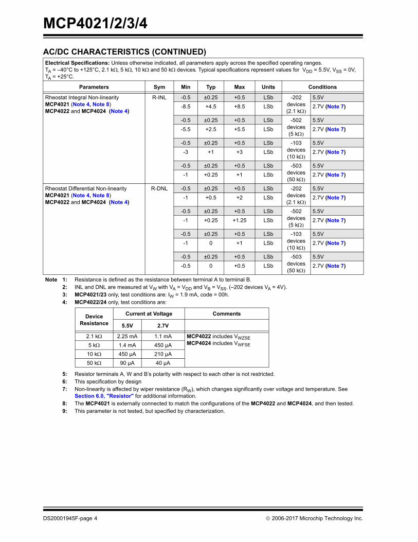
MCP4021/2/3/4
Rheostat Integral Non-linearity MCP4021 (Note 4, Note 8) MCP4022 and MCP4024 (Note 4)
R-INL -0.5 ±0.25 +0.5 LSb -202devices(2.1 k
5.5V
-8.5 +4.5 +8.5 LSb 2.7V (Note 7)
-0.5 ±0.25 +0.5 LSb -502devices(5 k
5.5V
-5.5 +2.5 +5.5 LSb 2.7V (Note 7)
-0.5 ±0.25 +0.5 LSb -103devices(10 k
5.5V
-3 +1 +3 LSb 2.7V (Note 7)
-0.5 ±0.25 +0.5 LSb -503devices(50 k
5.5V
-1 +0.25 +1 LSb 2.7V (Note 7)
Rheostat Differential Non-linearity MCP4021 (Note 4, Note 8) MCP4022 and MCP4024 (Note 4)
R-DNL -0.5 ±0.25 +0.5 LSb -202devices(2.1 k
5.5V
-1 +0.5 +2 LSb 2.7V (Note 7)
-0.5 ±0.25 +0.5 LSb -502devices(5 k
5.5V
-1 +0.25 +1.25 LSb 2.7V (Note 7)
-0.5 ±0.25 +0.5 LSb -103devices(10 k
5.5V
-1 0 +1 LSb 2.7V (Note 7)
-0.5 ±0.25 +0.5 LSb -503devices(50 k
5.5V
-0.5 0 +0.5 LSb 2.7V (Note 7)
AC/DC CHARACTERISTICS (CONTINUED)Electrical Specifications: Unless otherwise indicated, all parameters apply across the specified operating ranges.TA = –40°C to +125°C, 2.1 k5 k10 kand50 kdevicesTypical specifications represent values for VDD = 5.5V, VSS = 0V,TA = +25°C.
Parameters Sym Min Typ Max Units Conditions
Note 1: Resistance is defined as the resistance between terminal A to terminal B.2: INL and DNL are measured at VW with VA = VDD and VB = VSS. (–202 devices VA = 4V).3: MCP4021/23 only, test conditions are: IW = 1.9 mA, code = 00h.4: MCP4022/24 only, test conditions are:
5: Resistor terminals A, W and B’s polarity with respect to each other is not restricted.6: This specification by design7: Non-linearity is affected by wiper resistance (RW), which changes significantly over voltage and temperature. See
Section 6.0, "Resistor" for additional information.8: The MCP4021 is externally connected to match the configurations of the MCP4022 and MCP4024, and then tested.9: This parameter is not tested, but specified by characterization.
Device Resistance
Current at Voltage Comments
5.5V 2.7V
2.1 k 2.25 mA 1.1 mA MCP4022 includes VWZSE MCP4024 includes VWFSE 5 k 1.4 mA 450 µA
10 k 450 µA 210 µA
50 k 90 µA 40 µA
DS20001945F-page 4 2006-2017 Microchip Technology Inc.
MCP4021/2/3/4
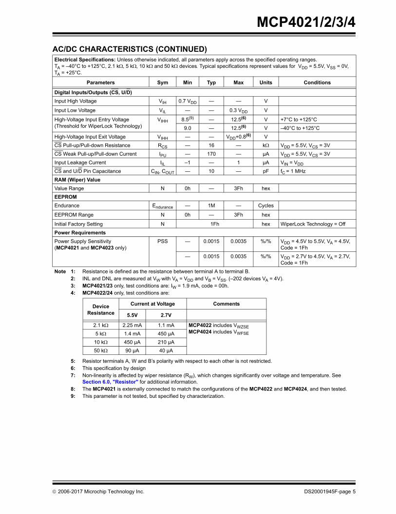
Digital Inputs/Outputs (CS, U/D)
Input High Voltage VIH 0.7 VDD — — V
Input Low Voltage VIL — — 0.3 VDD V
High-Voltage Input Entry Voltage (Threshold for WiperLock Technology)
VIHH 8.5(9) — 12.5(6) V +7°C to +125°C
9.0 — 12.5(6) V –40°C to +125°C
High-Voltage Input Exit Voltage VIHH — — VDD+0.8(6) V
CS Pull-up/Pull-down Resistance RCS — 16 — k VDD = 5.5V, VCS = 3V
CS Weak Pull-up/Pull-down Current IPU — 170 — µA VDD = 5.5V, VCS = 3V
Input Leakage Current IIL –1 — 1 µA VIN = VDD
CS and U/D Pin Capacitance CIN, COUT — 10 — pF fC = 1 MHz
RAM (Wiper) Value
Value Range N 0h — 3Fh hex
EEPROM
Endurance Endurance — 1M — Cycles
EEPROM Range N 0h — 3Fh hex
Initial Factory Setting N 1Fh hex WiperLock Technology = Off
Power Requirements
Power Supply Sensitivity (MCP4021 and MCP4023 only)
PSS — 0.0015 0.0035 %/% VDD = 4.5V to 5.5V, VA = 4.5V,Code = 1Fh
— 0.0015 0.0035 %/% VDD = 2.7V to 4.5V, VA = 2.7V,Code = 1Fh
AC/DC CHARACTERISTICS (CONTINUED)Electrical Specifications: Unless otherwise indicated, all parameters apply across the specified operating ranges.TA = –40°C to +125°C, 2.1 k5 k10 kand50 kdevicesTypical specifications represent values for VDD = 5.5V, VSS = 0V,TA = +25°C.
Parameters Sym Min Typ Max Units Conditions
Note 1: Resistance is defined as the resistance between terminal A to terminal B.2: INL and DNL are measured at VW with VA = VDD and VB = VSS. (–202 devices VA = 4V).3: MCP4021/23 only, test conditions are: IW = 1.9 mA, code = 00h.4: MCP4022/24 only, test conditions are:
5: Resistor terminals A, W and B’s polarity with respect to each other is not restricted.6: This specification by design7: Non-linearity is affected by wiper resistance (RW), which changes significantly over voltage and temperature. See
Section 6.0, "Resistor" for additional information.8: The MCP4021 is externally connected to match the configurations of the MCP4022 and MCP4024, and then tested.9: This parameter is not tested, but specified by characterization.
Device Resistance
Current at Voltage Comments
5.5V 2.7V
2.1 k 2.25 mA 1.1 mA MCP4022 includes VWZSE MCP4024 includes VWFSE 5 k 1.4 mA 450 µA
10 k 450 µA 210 µA
50 k 90 µA 40 µA
2006-2017 Microchip Technology Inc. DS20001945F-page 5

MCP4021/2/3/4
FIGURE 1-1: Increment Timing Waveform.
CS
U/D
tLCUR
tLO
tHI
tLUC
W
tCSHI
tS
1/fUD
tCSLO
tS
tLCUFtLUC tLCUF
SERIAL TIMING CHARACTERISTICS
Electrical Specifications: Unless otherwise noted, all parameters apply across the specified operating ranges.Extended (E): VDD = +2.7V to 5.5V, TA = -40°C to +125°C.
Parameters Sym Min Typ Max Units Conditions
CS Low Time tCSLO 5 — — µs
CS High Time tCSHI 500 — — ns
U/D to CS Hold Time tLUC 500 — — ns
CS to U/D Low Setup Time tLCUF 500 — — ns
CS to U/D High Setup Time tLCUR 3 — — µs
U/D High Time tHI 500 — — ns
U/D Low Time tLO 500 — — ns
Up/Down Toggle Frequency fUD — — 1 MHz
Wiper Settling Time tS 0.5 — — µs 2.1 k CL = 100 pF
1 — — µs 5 k CL = 100 pF
2 — — µs 10 k CL = 100 pF
10 5 — µs 50 k CL = 100 pF
Wiper Response on Power-Up tPU — 200 — ns
Internal EEPROM Write Time twc — — 5 ms @25°C
— — 10 ms -40°C to +125°C
DS20001945F-page 6 2006-2017 Microchip Technology Inc.

MCP4021/2/3/4
FIGURE 1-2: Decrement Timing Waveform.
CS
U/D
tLCUR
tHI
tLO
W
tS
tCSLO
tLUC
tCSHI
tLUC tLCUF
tS
1/fUD
SERIAL TIMING CHARACTERISTICS
Electrical Specifications: Unless otherwise noted, all parameters apply across the specified operating ranges.Extended (E): VDD = +2.7V to 5.5V, TA = –40°C to +125°C.
Parameters Sym Min Typ Max Units Conditions
CS Low Time tCSLO 5 — — µs
CS High Time tCSHI 500 — — ns
U/D to CS Hold Time tLUC 500 — — ns
CS to U/D Low Setup Time tLCUF 500 — — ns
CS to U/D High Setup Time tLCUR 3 — — µs
U/D High Time tHI 500 — — ns
U/D Low Time tLO 500 — — ns
Up/Down Toggle Frequency fUD — — 1 MHz
Wiper Settling Time tS 0.5 — — µs 2.1 k CL = 100 pF
1 — — µs 5 k CL = 100 pF
2 — — µs 10 k CL = 100 pF
10 5 — µs 50 k CL = 100 pF
Wiper Response on Power-Up tPU — 200 — ns
Internal EEPROM Write Time twc — — 5 ms @25°C
— — 10 ms -40°C to +125°C
2006-2017 Microchip Technology Inc. DS20001945F-page 7
MCP4021/2/3/4
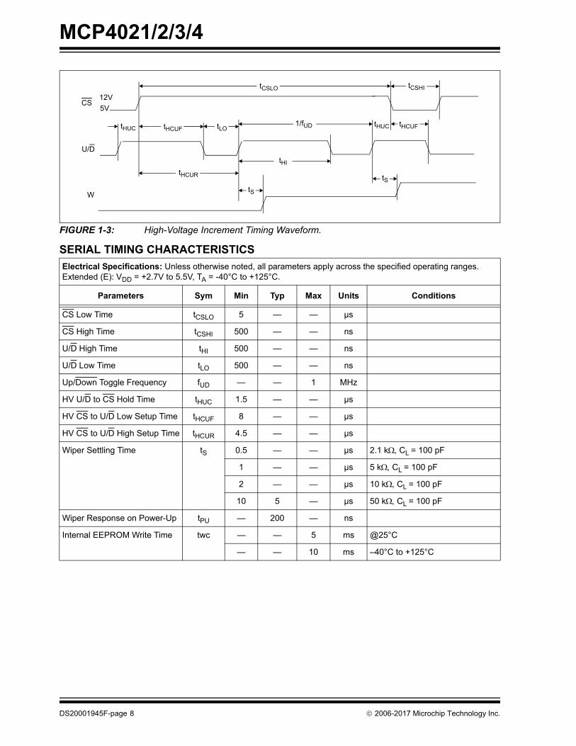
FIGURE 1-3: High-Voltage Increment Timing Waveform.
CS
U/D
tHCUR
tLO
tHI
tHUC
W
tCSHI
tS
1/fUD
tCSLO
tS
tHCUFtHUC tHCUF
5V
12V
SERIAL TIMING CHARACTERISTICS
Electrical Specifications: Unless otherwise noted, all parameters apply across the specified operating ranges.Extended (E): VDD = +2.7V to 5.5V, TA = -40°C to +125°C.
Parameters Sym Min Typ Max Units Conditions
CS Low Time tCSLO 5 — — µs
CS High Time tCSHI 500 — — ns
U/D High Time tHI 500 — — ns
U/D Low Time tLO 500 — — ns
Up/Down Toggle Frequency fUD — — 1 MHz
HV U/D to CS Hold Time tHUC 1.5 — — µs
HV CS to U/D Low Setup Time tHCUF 8 — — µs
HV CS to U/D High Setup Time tHCUR 4.5 — — µs
Wiper Settling Time tS 0.5 — — µs 2.1 k CL = 100 pF
1 — — µs 5 k CL = 100 pF
2 — — µs 10 k CL = 100 pF
10 5 — µs 50 k CL = 100 pF
Wiper Response on Power-Up tPU — 200 — ns
Internal EEPROM Write Time twc — — 5 ms @25°C
— — 10 ms –40°C to +125°C
DS20001945F-page 8 2006-2017 Microchip Technology Inc.
MCP4021/2/3/4
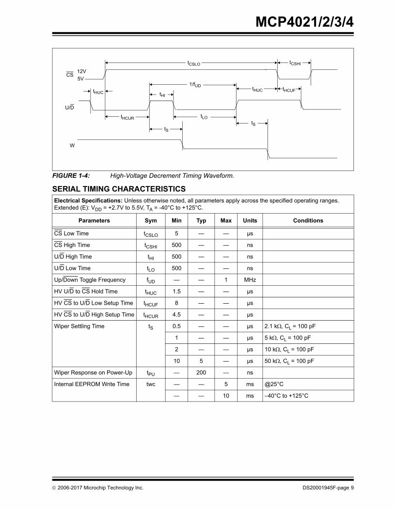
FIGURE 1-4: High-Voltage Decrement Timing Waveform.
CS
U/D
tHCUR
tHI
tLO
W
tS
tCSLO
tHUC
tCSHI
tHUC tHCUF
tS
5V
12V
1/fUD
SERIAL TIMING CHARACTERISTICS
Electrical Specifications: Unless otherwise noted, all parameters apply across the specified operating ranges.Extended (E): VDD = +2.7V to 5.5V, TA = -40°C to +125°C.
Parameters Sym Min Typ Max Units Conditions
CS Low Time tCSLO 5 — — µs
CS High Time tCSHI 500 — — ns
U/D High Time tHI 500 — — ns
U/D Low Time tLO 500 — — ns
Up/Down Toggle Frequency fUD — — 1 MHz
HV U/D to CS Hold Time tHUC 1.5 — — µs
HV CS to U/D Low Setup Time tHCUF 8 — — µs
HV CS to U/D High Setup Time tHCUR 4.5 — — µs
Wiper Settling Time tS 0.5 — — µs 2.1 k CL = 100 pF
1 — — µs 5 k CL = 100 pF
2 — — µs 10 k CL = 100 pF
10 5 — µs 50 k CL = 100 pF
Wiper Response on Power-Up tPU — 200 — ns
Internal EEPROM Write Time twc — — 5 ms @25°C
— — 10 ms –40°C to +125°C
2006-2017 Microchip Technology Inc. DS20001945F-page 9
MCP4021/2/3/4
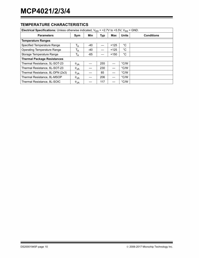
TEMPERATURE CHARACTERISTICS Electrical Specifications: Unless otherwise indicated, VDD = +2.7V to +5.5V, VSS = GND.
Parameters Sym Min Typ Max Units Conditions
Temperature Ranges
Specified Temperature Range TA -40 — +125 °C
Operating Temperature Range TA -40 — +125 °C
Storage Temperature Range TA -65 — +150 °C
Thermal Package Resistances
Thermal Resistance, 5L-SOT-23 JA — 255 — °C/W
Thermal Resistance, 6L-SOT-23 JA — 230 — °C/W
Thermal Resistance, 8L-DFN (2x3) JA — 85 — °C/W
Thermal Resistance, 8L-MSOP JA — 206 — °C/W
Thermal Resistance, 8L-SOIC JA — 117 — °C/W
DS20001945F-page 10 2006-2017 Microchip Technology Inc.

MCP4021/2/3/4
2.0 TYPICAL PERFORMANCE CURVES
Note: Unless otherwise indicated, TA = +25°C, VDD = 5V, VSS = 0V.
FIGURE 2-1: Device Current (IDD) vs. U/D Frequency (fU/D) and Ambient Temperature (VDD = 2.7V and 5.5V).
FIGURE 2-2: Write Current (IWRITE) vs. Ambient Temperature and VDD.
FIGURE 2-3: Device Current (ISHDN) vs. Ambient Temperature and VDD. (CS = VDD).
FIGURE 2-4: CS Pull-up/Pull-down Resistance (RCS) and Current (ICS) vs. CS Input Voltage (VCS) (VDD = 5.5V).
FIGURE 2-5: CS High Input Entry/Exit Threshold vs. Ambient Temperature and VDD.
Note: The graphs and tables provided following this note are a statistical summary based on a limited number ofsamples and are provided for informational purposes only. The performance characteristics listed hereinare not tested or guaranteed. In some graphs or tables, the data presented may be outside the specifiedoperating range (e.g., outside specified power supply range) and therefore outside the warranted range.
0
10
20
30
40
50
60
70
80
0.20 0.40 0.60 0.80 1.00fU/D (MHz)
Dev
ice
Cur
rent
(ID
D) (
µA)
2.7V -40°C2.7V 25°C2.7V 85°C2.7V 125°C5.5V -40°C5.5V 25°C5.5V 85°C5.5V 125°C
0.0
100.0
200.0
300.0
400.0
500.0
600.0
-40 25 85 125Ambient Temperature (°C)
Dev
ice
Cur
rent
(ID
D) (
µA)
VDD = 2.7V
VDD = 5.5V
0.0
0.1
0.2
0.3
0.4
0.5
0.6
0.7
0.8
-40 25 85 125Ambient Temperature (°C)
Dev
ice
Cur
rent
(ID
D) (
µA)
VDD = 2.7V
VDD = 5.5V
0
50
100
150
200
250
9 8 7 6 5 4 3 2 1VCS (V)
RC
S (k
Ohm
s)
-1000-800-600-400-20002004006008001000
Ics
(µA
)
ICS
RCS
0
2
4
6
8
10
12
-40 -20 0 20 40 60 80 100 120Ambient Temperature (°C)
CS
V PP
Thre
shol
d (V
)
1.8V Entry2.7V Entry5.5V Entry1.8V Exit2.7V Exit5.5V Exit
2006-2017 Microchip Technology Inc. DS20001945F-page 11
MCP4021/2/3/4
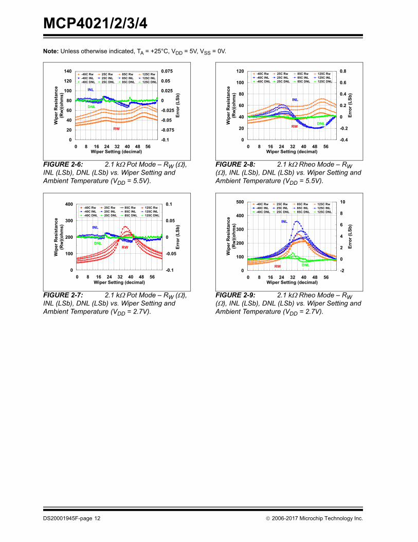
Note: Unless otherwise indicated, TA = +25°C, VDD = 5V, VSS = 0V.
FIGURE 2-6: 2.1 k Pot Mode – RW (), INL (LSb), DNL (LSb) vs. Wiper Setting and Ambient Temperature (VDD = 5.5V).
FIGURE 2-7: 2.1 k Pot Mode – RW (), INL (LSb), DNL (LSb) vs. Wiper Setting and Ambient Temperature (VDD = 2.7V).
FIGURE 2-8: 2.1 k Rheo Mode – RW (), INL (LSb), DNL (LSb) vs. Wiper Setting and Ambient Temperature (VDD = 5.5V).
FIGURE 2-9: 2.1 k Rheo Mode – RW (), INL (LSb), DNL (LSb) vs. Wiper Setting and Ambient Temperature (VDD = 2.7V).
0
20
40
60
80
100
120
140
0 8 16 24 32 40 48 56Wiper Setting (decimal)
Wip
er R
esis
tanc
e (R
w)(o
hms)
-0.1
-0.075
-0.05
-0.025
0
0.025
0.05
0.075
Erro
r (LS
b)
-40C Rw 25C Rw 85C Rw 125C Rw-40C INL 25C INL 85C INL 125C INL-40C DNL 25C DNL 85C DNL 125C DNL
INL
DNL
RW
0
100
200
300
400
0 8 16 24 32 40 48 56Wiper Setting (decimal)
Wip
er R
esis
tanc
e (R
w)(o
hms)
-0.1
-0.05
0
0.05
0.1
Erro
r (LS
b)
-40C Rw 25C Rw 85C Rw 125C Rw-40C INL 25C INL 85C INL 125C INL-40C DNL 25C DNL 85C DNL 125C DNL
INL
DNLRW
0
20
40
60
80
100
120
0 8 16 24 32 40 48 56Wiper Setting (decimal)
Wip
er R
esis
tanc
e (R
w)(o
hms)
-0.4
-0.2
0
0.2
0.4
0.6
0.8
Erro
r (LS
b)
-40C Rw 25C Rw 85C Rw 125C Rw-40C INL 25C INL 85C INL 125C INL-40C DNL 25C DNL 85C DNL 125C DNL
INL
DNLRW
0
100
200
300
400
500
0 8 16 24 32 40 48 56Wiper Setting (decimal)
Wip
er R
esis
tanc
e (R
w)(o
hms)
-2
0
2
4
6
8
10
Erro
r (LS
b)
-40C Rw 25C Rw 85C Rw 125C Rw-40C INL 25C INL 85C INL 125C INL-40C DNL 25C DNL 85C DNL 125C DNL
INL
DNLRW
DS20001945F-page 12 2006-2017 Microchip Technology Inc.

MCP4021/2/3/4
Note: Unless otherwise indicated, TA = +25°C, VDD = 5V, VSS = 0V.
FIGURE 2-10: 2.1 k – Nominal Resistance () vs. Ambient Temperature and VDD.
FIGURE 2-11: 2.1 k – RWB () vs. Wiper Setting and Ambient Temperature.
2000
2020
2040
2060
2080
-40 0 40 80 120Ambient Temperature (°C)
Nom
inal
Res
ista
nce
(RA
B)(O
hms)
VDD = 2.7V
VDD = 5.5V
0
500
1000
1500
2000
2500
0 8 16 24 32 40 48 56 64Wiper Setting (decimal)
RW
B (O
hms)
-40°C25°C85°C125°C
2006-2017 Microchip Technology Inc. DS20001945F-page 13

MCP4021/2/3/4
Note: Unless otherwise indicated, TA = +25°C, VDD = 5V, VSS = 0V.
FIGURE 2-12: 2.1 k – Low-Voltage Decrement Wiper Settling Time (VDD = 2.7V).
FIGURE 2-13: 2.1 k – Low-Voltage Decrement Wiper Settling Time (VDD = 5.5V).
FIGURE 2-14: 2.1 k – Power-Up Wiper Response Time.
FIGURE 2-15: 2.1 k – Low-Voltage Increment Wiper Settling Time (VDD = 2.7V).
FIGURE 2-16: 2.1 k – Low-Voltage Increment Wiper Settling Time (VDD = 5.5V).
U/D
WIPER
U/D
WIPER
WIPER
VDD
U/D
WIPER
U/D
WIPER
DS20001945F-page 14 2006-2017 Microchip Technology Inc.

MCP4021/2/3/4
Note: Unless otherwise indicated, TA = +25°C, VDD = 5V, VSS = 0V.
FIGURE 2-17: 5 k Pot Mode – RW (), INL (LSb), DNL (LSb) vs. Wiper Setting and Ambient Temperature (VDD = 5.5V).
FIGURE 2-18: 5 k Pot Mode – RW (), INL (LSb), DNL (LSb) vs. Wiper Setting and Ambient Temperature (VDD = 2.7V).
FIGURE 2-19: 5 k Rheo Mode – RW (), INL (LSb), DNL (LSb) vs. Wiper Setting and Ambient Temperature (VDD = 5.5V).
FIGURE 2-20: 5 k Rheo Mode – RW (), INL (LSb), DNL (LSb) vs. Wiper Setting and Ambient Temperature (VDD = 2.7V).
0
20
40
60
80
100
120
140
0 8 16 24 32 40 48 56Wiper Setting (decimal)
Wip
er R
esis
tanc
e (R
w)(o
hms)
-0.1
-0.075
-0.05
-0.025
0
0.025
0.05
0.075
Erro
r (LS
b)
-40C Rw 25C Rw 85C Rw 125C Rw-40C INL 25C INL 85C INL 125C INL-40C DNL 25C DNL 85C DNL 125C DNL
INL
DNL
RW
050
100150200250300350400450
0 8 16 24 32 40 48 56Wiper Setting (decimal)
Wip
er R
esis
tanc
e (R
w)(o
hms)
-0.125-0.1-0.075-0.05-0.02500.0250.050.0750.1
Erro
r (LS
b)
-40C Rw 25C Rw 85C Rw 125C Rw-40C INL 25C INL 85C INL 125C INL-40C DNL 25C DNL 85C DNL 125C DNL
INL
DNL
RW
0
20
40
60
80
100
120
0 8 16 24 32 40 48 56Wiper Setting (decimal)
Wip
er R
esis
tanc
e (R
w)(o
hms)
-0.6
-0.4
-0.2
0
0.2
0.4
0.6
Erro
r (LS
b)
-40C Rw 25C Rw 85C Rw 125C Rw-40C INL 25C INL 85C INL 125C INL-40C DNL 25C DNL 85C DNL 125C DNL
INL
DNL
RW
0
100
200
300
400
500
600
0 8 16 24 32 40 48 56Wiper Setting (decimal)
Wip
er R
esis
tanc
e (R
w)(o
hms)
-1
0
1
2
3
4
5
Erro
r (LS
b)
-40C Rw 25C Rw 85C Rw 125C Rw-40C INL 25C INL 85C INL 125C INL-40C DNL 25C DNL 85C DNL 125C DNL
INL
DNLRW
2006-2017 Microchip Technology Inc. DS20001945F-page 15

MCP4021/2/3/4
Note: Unless otherwise indicated, TA = +25°C, VDD = 5V, VSS = 0V.
FIGURE 2-21: 5 k – Nominal Resistance () vs. Ambient Temperature and VDD.
FIGURE 2-22: 5 k – RWB () vs. Wiper Setting and Ambient Temperature.
4800
4825
4850
4875
4900
4925
4950
-40 -20 0 20 40 60 80 100 120Ambient Temperature (°C)
Nom
inal
Res
ista
nce
(RA
B)(O
hms)
2.7V Vdd5.5V Vdd
VDD = 2.7V
VDD = 5.5V
0
1000
2000
3000
4000
5000
6000
0 8 16 24 32 40 48 56 64Wiper Setting (decimal)
RW
B (O
hms)
-40°C25°C85°C125°C
DS20001945F-page 16 2006-2017 Microchip Technology Inc.
MCP4021/2/3/4
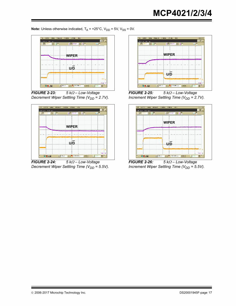
Note: Unless otherwise indicated, TA = +25°C, VDD = 5V, VSS = 0V.
FIGURE 2-23: 5 k – Low-Voltage Decrement Wiper Settling Time (VDD = 2.7V).
FIGURE 2-24: 5 k – Low-Voltage Decrement Wiper Settling Time (VDD = 5.5V).
FIGURE 2-25: 5 k – Low-Voltage Increment Wiper Settling Time (VDD = 2.7V).
FIGURE 2-26: 5 k – Low-Voltage Increment Wiper Settling Time (VDD = 5.5V).
U/D
WIPER
U/D
WIPER
U/D
WIPER
U/D
WIPER
2006-2017 Microchip Technology Inc. DS20001945F-page 17
MCP4021/2/3/4
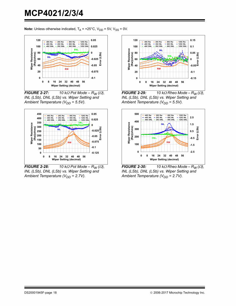
Note: Unless otherwise indicated, TA = +25°C, VDD = 5V, VSS = 0V.
FIGURE 2-27: 10 k Pot Mode – RW (), INL (LSb), DNL (LSb) vs. Wiper Setting and Ambient Temperature (VDD = 5.5V).
FIGURE 2-28: 10 k Pot Mode – RW (), INL (LSb), DNL (LSb) vs. Wiper Setting and Ambient Temperature (VDD = 2.7V).
FIGURE 2-29: 10 k Rheo Mode – RW (), INL (LSb), DNL (LSb) vs. Wiper Setting and Ambient Temperature (VDD = 5.5V).
FIGURE 2-30: 10 k Rheo Mode – RW (), INL (LSb), DNL (LSb) vs. Wiper Setting and Ambient Temperature (VDD = 2.7V).
0
20
40
60
80
100
120
0 8 16 24 32 40 48 56Wiper Setting (decimal)
Wip
er R
esis
tanc
e (R
w)(o
hms)
-0.1
-0.075
-0.05
-0.025
0
0.025
0.05
Erro
r (LS
b)
-40C Rw 25C Rw 85C Rw 125C Rw-40C INL 25C INL 85C INL 125C INL-40C DNL 25C DNL 85C DNL 125C DNL
INL
DNL
RW
050
100150200250300350400450
0 8 16 24 32 40 48 56Wiper Setting (decimal)
Wip
er R
esis
tanc
e (R
w)(o
hms)
-0.125
-0.1
-0.075
-0.05
-0.025
0
0.025
0.05
Erro
r (LS
b)
-40C Rw 25C Rw 85C Rw 125C Rw-40C INL 25C INL 85C INL 125C INL-40C DNL 25C DNL 85C DNL 125C DNL
INL
DNL
RW
0
20
40
60
80
100
120
0 8 16 24 32 40 48 56Wiper Setting (decimal)
Wip
er R
esis
tanc
e (R
w)(o
hms)
-0.15
-0.1
-0.05
0
0.05
0.1
0.15
Erro
r (LS
b)
-40C Rw 25C Rw 85C Rw 125C Rw-40C INL 25C INL 85C INL 125C INL-40C DNL 25C DNL 85C DNL 125C DNL
INL
DNL
RW
0
100
200
300
400
500
0 8 16 24 32 40 48 56Wiper Setting (decimal)
Wip
er R
esis
tanc
e (R
w)(o
hms)
-2.5
-1.5
-0.5
0.5
1.5
2.5
Erro
r (LS
b)
-40C Rw 25C Rw 85C Rw 125C Rw-40C INL 25C INL 85C INL 125C INL-40C DNL 25C DNL 85C DNL 125C DNL
INL
DNL
RW
DS20001945F-page 18 2006-2017 Microchip Technology Inc.
MCP4021/2/3/4
Note: Unless otherwise indicated, TA = +25°C, VDD = 5V, VSS = 0V.
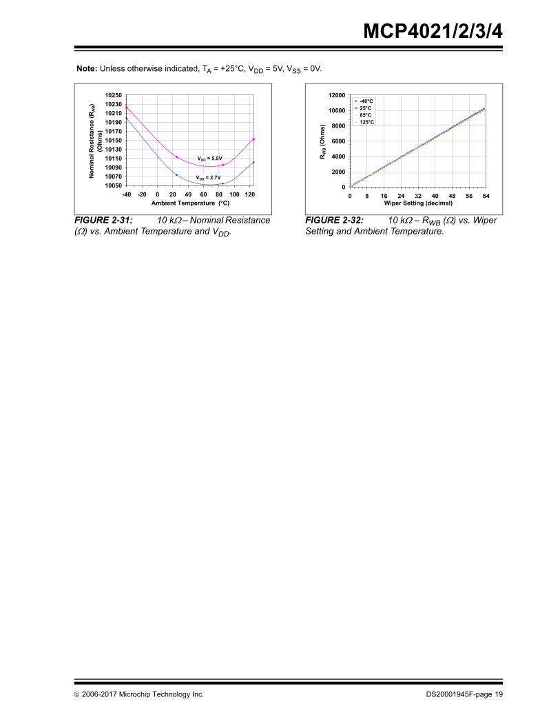
FIGURE 2-31: 10 k – Nominal Resistance () vs. Ambient Temperature and VDD.
FIGURE 2-32: 10 k – RWB () vs. Wiper Setting and Ambient Temperature.
1005010070100901011010130101501017010190102101023010250
-40 -20 0 20 40 60 80 100 120Ambient Temperature (°C)
Nom
inal
Res
ista
nce
(RA
B)(O
hms)
VDD = 2.7V
VDD = 5.5V
0
2000
4000
6000
8000
10000
12000
0 8 16 24 32 40 48 56 64Wiper Setting (decimal)
RW
B (O
hms)
-40°C25°C85°C125°C
2006-2017 Microchip Technology Inc. DS20001945F-page 19
MCP4021/2/3/4
Note: Unless otherwise indicated, TA = +25°C, VDD = 5V, VSS = 0V.
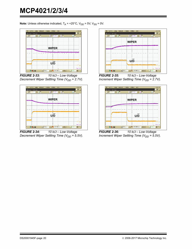
FIGURE 2-33: 10 k – Low-Voltage Decrement Wiper Settling Time (VDD = 2.7V).
FIGURE 2-34: 10 k – Low-Voltage Decrement Wiper Settling Time (VDD = 5.5V).
FIGURE 2-35: 10 k – Low-Voltage Increment Wiper Settling Time (VDD = 2.7V).
FIGURE 2-36: 10 k – Low-Voltage Increment Wiper Settling Time (VDD = 5.5V).
U/D
WIPER
U/D
WIPER
U/D
WIPER
U/D
WIPER
DS20001945F-page 20 2006-2017 Microchip Technology Inc.

MCP4021/2/3/4
Note: Unless otherwise indicated, TA = +25°C, VDD = 5V, VSS = 0V.
FIGURE 2-37: 50 k Pot Mode – RW (), INL (LSb), DNL (LSb) vs. Wiper Setting and Ambient Temperature (VDD = 5.5V).
FIGURE 2-38: 50 k Pot Mode – RW (), INL (LSb), DNL (LSb) vs. Wiper Setting and Ambient Temperature (VDD = 2.7V).
FIGURE 2-39: 50 k Rheo Mode – RW (), INL (LSb), DNL (LSb) vs. Wiper Setting and Ambient Temperature (VDD = 5.5V).
FIGURE 2-40: 50 k Rheo Mode – RW (), INL (LSb), DNL (LSb) vs. Wiper Setting and Ambient Temperature (VDD = 2.7V).
0
40
80
120
160
200
0 8 16 24 32 40 48 56Wiper Setting (decimal)
Wip
er R
esis
tanc
e (R
w)(o
hms)
-0.15
-0.1
-0.05
0
0.05
0.1
Erro
r (LS
b)
-40C Rw 25C Rw 85C Rw 125C Rw-40C INL 25C INL 85C INL 125C INL-40C DNL 25C DNL 85C DNL 125C DNL
INL
DNL
RW
0
100
200
300
400
500
600
0 8 16 24 32 40 48 56Wiper Setting (decimal)
Wip
er R
esis
tanc
e (R
w)(o
hms)
-0.1
-0.075
-0.05
-0.025
0
0.025
0.05
Erro
r (LS
b)
-40C Rw 25C Rw 85C Rw 125C Rw-40C INL 25C INL 85C INL 125C INL-40C DNL 25C DNL 85C DNL 125C DNL
INL
DNL
RW
0
50
100
150
200
0 8 16 24 32 40 48 56Wiper Setting (decimal)
Wip
er R
esis
tanc
e (R
w)(o
hms)
-0.1
-0.05
0
0.05
0.1
0.15
Erro
r (LS
b)
-40C Rw 25C Rw 85C Rw 125C Rw-40C INL 25C INL 85C INL 125C INL-40C DNL 25C DNL 85C DNL 125C DNL
INL
DNL
RW
0
100
200
300
400
500
600
0 8 16 24 32 40 48 56Wiper Setting (decimal)
Wip
er R
esis
tanc
e (R
w)(o
hms)
-1.5
-1
-0.5
0
0.5
1
1.5
Erro
r (LS
b)
-40C Rw 25C Rw 85C Rw 125C Rw-40C INL 25C INL 85C INL 125C INL-40C DNL 25C DNL 85C DNL 125C DNL
INL
DNL
RW
2006-2017 Microchip Technology Inc. DS20001945F-page 21
MCP4021/2/3/4
Note: Unless otherwise indicated, TA = +25°C, VDD = 5V, VSS = 0V.
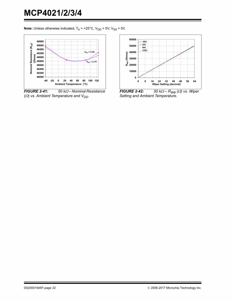
FIGURE 2-41: 50 k – Nominal Resistance () vs. Ambient Temperature and VDD.
FIGURE 2-42: 50 k – RWB () vs. Wiper Setting and Ambient Temperature.
48000482004840048600488004900049200494004960049800
-40 -20 0 20 40 60 80 100 120Ambient Temperature (°C)
Nom
inal
Res
ista
nce
(RA
B)(O
hms)
VDD = 2.7V
VDD = 5.5V
0
10000
20000
30000
40000
50000
60000
0 8 16 24 32 40 48 56 64Wiper Setting (decimal)
RW
B (O
hms)
-40C25C85C125C
DS20001945F-page 22 2006-2017 Microchip Technology Inc.
MCP4021/2/3/4
Note: Unless otherwise indicated, TA = +25°C, VDD = 5V, VSS = 0V.
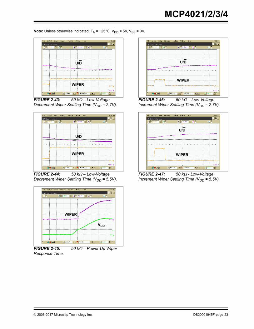
FIGURE 2-43: 50 k – Low-Voltage Decrement Wiper Settling Time (VDD = 2.7V).
FIGURE 2-44: 50 k – Low-Voltage Decrement Wiper Settling Time (VDD = 5.5V).
FIGURE 2-45: 50 k – Power-Up Wiper Response Time.
FIGURE 2-46: 50 k – Low-Voltage Increment Wiper Settling Time (VDD = 2.7V).
FIGURE 2-47: 50 k - Low-Voltage Increment Wiper Settling Time (VDD = 5.5V).
U/D
WIPER
U/D
WIPER
VDD
WIPER
U/D
WIPER
U/D
WIPER
2006-2017 Microchip Technology Inc. DS20001945F-page 23

MCP4021/2/3/4
Note: Unless otherwise indicated, TA = +25°C, VDD = 5V, VSS = 0V.
FIGURE 2-48: -3 dB Bandwidth vs. Temperature.
FIGURE 2-49: -3 dB Bandwidth Test Circuit.
00.5
11.5
22.5
33.5
44.5
-40 25 125
Temperature (°C)
-3dB
Fre
quen
cy (M
Hz) 2.1 k
5 k
10 k
50 k
VIN
-
+
+5V
VOUT
2.5V DC
OFFSETGND
A
B
DUT
W~
DS20001945F-page 24 2006-2017 Microchip Technology Inc.
MCP4021/2/3/4
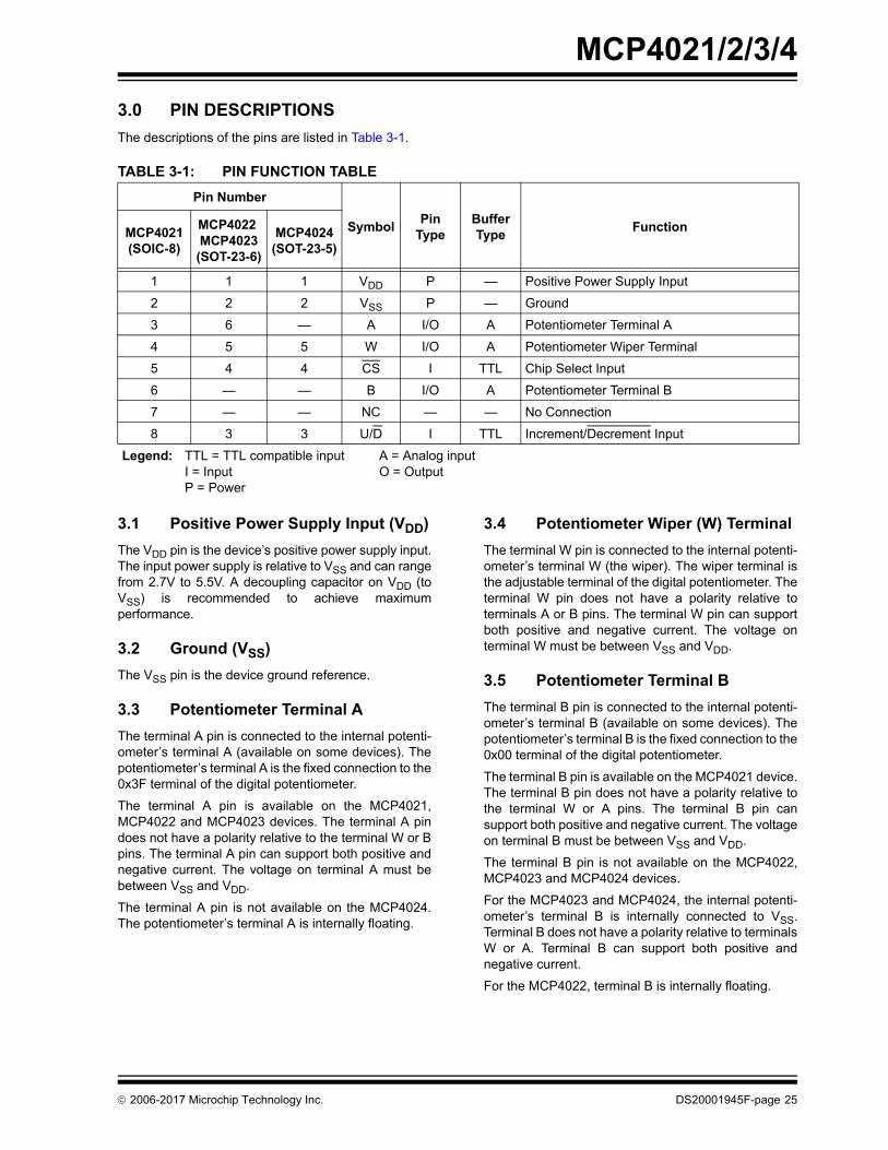
3.0 PIN DESCRIPTIONS
The descriptions of the pins are listed in Table 3-1.
TABLE 3-1: PIN FUNCTION TABLE
3.1 Positive Power Supply Input (VDD)
The VDD pin is the device’s positive power supply input.The input power supply is relative to VSS and can rangefrom 2.7V to 5.5V. A decoupling capacitor on VDD (toVSS) is recommended to achieve maximumperformance.
3.2 Ground (VSS)
The VSS pin is the device ground reference.
3.3 Potentiometer Terminal A
The terminal A pin is connected to the internal potenti-ometer’s terminal A (available on some devices). Thepotentiometer’s terminal A is the fixed connection to the0x3F terminal of the digital potentiometer.
The terminal A pin is available on the MCP4021,MCP4022 and MCP4023 devices. The terminal A pindoes not have a polarity relative to the terminal W or Bpins. The terminal A pin can support both positive andnegative current. The voltage on terminal A must bebetween VSS and VDD.
The terminal A pin is not available on the MCP4024.The potentiometer’s terminal A is internally floating.
3.4 Potentiometer Wiper (W) Terminal
The terminal W pin is connected to the internal potenti-ometer’s terminal W (the wiper). The wiper terminal isthe adjustable terminal of the digital potentiometer. Theterminal W pin does not have a polarity relative toterminals A or B pins. The terminal W pin can supportboth positive and negative current. The voltage onterminal W must be between VSS and VDD.
3.5 Potentiometer Terminal B
The terminal B pin is connected to the internal potenti-ometer’s terminal B (available on some devices). Thepotentiometer’s terminal B is the fixed connection to the0x00 terminal of the digital potentiometer.
The terminal B pin is available on the MCP4021 device.The terminal B pin does not have a polarity relative tothe terminal W or A pins. The terminal B pin cansupport both positive and negative current. The voltageon terminal B must be between VSS and VDD.
The terminal B pin is not available on the MCP4022,MCP4023 and MCP4024 devices.
For the MCP4023 and MCP4024, the internal potenti-ometer’s terminal B is internally connected to VSS.Terminal B does not have a polarity relative to terminalsW or A. Terminal B can support both positive andnegative current.
For the MCP4022, terminal B is internally floating.
Pin Number
SymbolPin
TypeBuffer Type
FunctionMCP4021 (SOIC-8)
MCP4022 MCP4023
(SOT-23-6)
MCP4024 (SOT-23-5)
1 1 1 VDD P — Positive Power Supply Input
2 2 2 VSS P — Ground
3 6 — A I/O A Potentiometer Terminal A
4 5 5 W I/O A Potentiometer Wiper Terminal
5 4 4 CS I TTL Chip Select Input
6 — — B I/O A Potentiometer Terminal B
7 — — NC — — No Connection
8 3 3 U/D I TTL Increment/Decrement Input
Legend: TTL = TTL compatible input A = Analog input I = Input O = Output P = Power
2006-2017 Microchip Technology Inc. DS20001945F-page 25

MCP4021/2/3/4
3.6 Chip Select (CS)
The CS pin is the chip select input. Forcing the CS pinto VIL enables the serial commands. These commandscan increment and decrement the wiper. Depending onthe command, the wiper may (or may not) be saved tononvolatile memory (EEPROM). Forcing the CS pin toVIHH enables the high-voltage serial commands. Thesecommands can increment and decrement the wiperand enable or disable the WiperLock technology. Thewiper is saved to nonvolatile memory (EEPROM).
The CS pin has an internal pull-up resistor. The resistorwill become “disabled” when the voltage on the CS pinis below the VIH level. This means that when the CS pinis “floating”, the CS pin will be pulled to the VIH level(serial communication (the U/D pin) is ignored). Andwhen the CS pin is driven low (VIL), the resistancebecomes very large to reduce the device currentconsumption when serial commands are occurring.See Figure 2-4 for additional information.
3.7 Increment/Decrement (U/D)
The U/D pin input is used to increment or decrementthe wiper on the digital potentiometer. An incrementmoves the wiper one step toward terminal A, while adecrement moves the wiper one step towardterminal B.
DS20001945F-page 26 2006-2017 Microchip Technology Inc.
MCP4021/2/3/4
4.0 GENERAL OVERVIEW
The MCP402X devices are general purpose digitalpotentiometers intended to be used in applicationswhere a programmable resistance with moderatebandwidth is desired.
Applications generally suited for the MCP402X devicesinclude:
• Set point or offset trimming
• Sensor calibration
• Selectable gain and offset amplifier designs
• Cost-sensitive mechanical trim pot replacement
The digital potentiometer is available in four nominalresistances (RAB), where the nominal resistance isdefined as the resistance between terminal A andterminal B. The four nominal resistances are 2.1 k,5 k, 10 k and 50 k
There are 63 resistors in a string between terminal Aand terminal B. The wiper can be set to tap onto any ofthese 63 resistors thus providing 64 possible settings(including terminal A and terminal B).
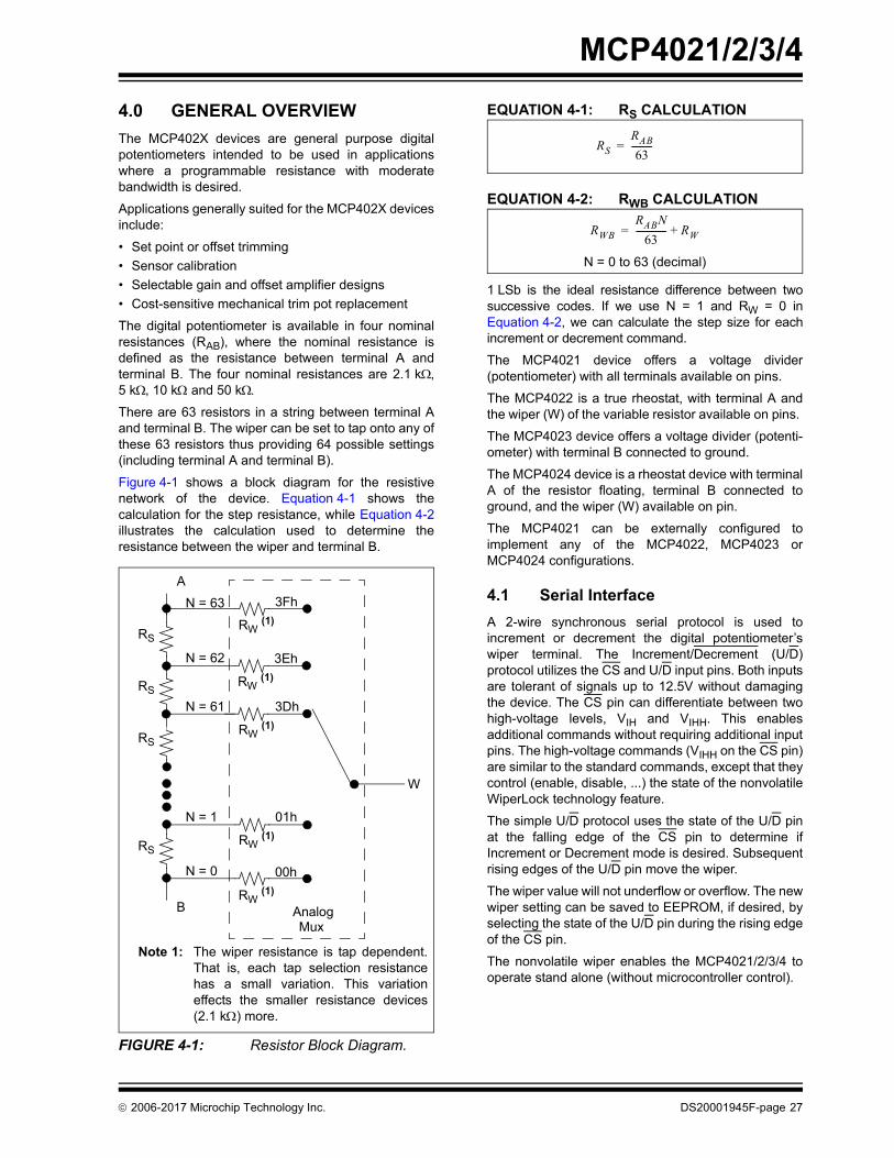
Figure 4-1 shows a block diagram for the resistivenetwork of the device. Equation 4-1 shows thecalculation for the step resistance, while Equation 4-2illustrates the calculation used to determine theresistance between the wiper and terminal B.
FIGURE 4-1: Resistor Block Diagram.
EQUATION 4-1: RS CALCULATION
EQUATION 4-2: RWB CALCULATION
1 LSb is the ideal resistance difference between twosuccessive codes. If we use N = 1 and RW = 0 inEquation 4-2, we can calculate the step size for eachincrement or decrement command.
The MCP4021 device offers a voltage divider(potentiometer) with all terminals available on pins.
The MCP4022 is a true rheostat, with terminal A andthe wiper (W) of the variable resistor available on pins.
The MCP4023 device offers a voltage divider (potenti-ometer) with terminal B connected to ground.
The MCP4024 device is a rheostat device with terminalA of the resistor floating, terminal B connected toground, and the wiper (W) available on pin.
The MCP4021 can be externally configured toimplement any of the MCP4022, MCP4023 orMCP4024 configurations.
4.1 Serial Interface
A 2-wire synchronous serial protocol is used toincrement or decrement the digital potentiometer’swiper terminal. The Increment/Decrement (U/D)protocol utilizes the CS and U/D input pins. Both inputsare tolerant of signals up to 12.5V without damagingthe device. The CS pin can differentiate between twohigh-voltage levels, VIH and VIHH. This enablesadditional commands without requiring additional inputpins. The high-voltage commands (VIHH on the CS pin)are similar to the standard commands, except that theycontrol (enable, disable, ...) the state of the nonvolatileWiperLock technology feature.
The simple U/D protocol uses the state of the U/D pinat the falling edge of the CS pin to determine ifIncrement or Decrement mode is desired. Subsequentrising edges of the U/D pin move the wiper.
The wiper value will not underflow or overflow. The newwiper setting can be saved to EEPROM, if desired, byselecting the state of the U/D pin during the rising edgeof the CS pin.
The nonvolatile wiper enables the MCP4021/2/3/4 tooperate stand alone (without microcontroller control).
RS
A
RS
RS
RS
B
N = 63
N = 62
N = 61
N = 1
N = 0
RW (1)
W
01h
AnalogMux
RW (1)
00h
RW (1)
3Dh
RW (1)
3Eh
RW (1)
3Fh
Note 1: The wiper resistance is tap dependent.That is, each tap selection resistancehas a small variation. This variationeffects the smaller resistance devices(2.1 k) more.
RSRAB63---------=
RWBRABN
63-------------- RW+=
N = 0 to 63 (decimal)
2006-2017 Microchip Technology Inc. DS20001945F-page 27

MCP4021/2/3/4
4.2 The WiperLock Technology
The MCP4021/2/3/4 device’s WiperLock technologyallows application-specific calibration settings to besecured in the EEPROM without requiring the use of anadditional write-protect pin.
The WiperLock technology prevents the serialcommands from doing the following:
• Incrementing or decrementing the wiper setting
• Writing the wiper setting to the nonvolatile memory
Enabling and disabling the WiperLock technologyfeature requires high-voltage serial commands(CS = VIHH). Incrementing and decrementing the wiperrequires high-voltage commands when the feature isenabled. The high-voltage threshold (VIHH) is intendedto prevent the wiper setting from being altered by noiseor intentional transitions on the U/D and CS pins, whilestill providing flexibility for production or calibrationenvironments.
Both the CS and U/D input pins are tolerant of signalsup to 12V. This allows the flexibility to multiplex thedigital pot’s control signals onto application signals formanufacturing/calibration.
4.3 Power-up
When the device powers up, the last saved wipersetting is restored.
While VDD < Vmin (2.7V), the electrical performancemay not meet the data sheet specifications (seeFigure 4-2). The wiper may be unknown or initialized tothe value stored in the EEPROM. Also the device maybe capable of incrementing, decrementing and writingto its EEPROM, if a valid command is detected on theCS and U/D pins.
The default settings of the MCP4021/2/3/4 device’sfrom the factory are shown in Table 4-1.
TABLE 4-1: DEFAULT FACTORY SETTINGS SELECTION
It is good practice in your manufacturing flow toconfigure the device to your desired settings.
4.4 Brown-Out
If the device VDD is below the specified minimumvoltage, care must be taken to ensure that the CS andU/D pins do not “create” any of the serial commands.
When the device VDD drops below Vmin (2.7V), theelectrical performance may not meet the data sheetspecifications (see Figure 4-2). The wiper may beunknown or initialized to the value stored in theEEPROM. Also the device may be capable ofincrementing, decrementing and writing to its EEPROMif a valid command is detected on the CS and U/D pins.
4.5 Serial Interface Inactive
The serial interface is inactive any time the CS pin is atVIH and all write cycles are completed.
FIGURE 4-2: Power-up and Brown-out.
Pa
cka
ge
Co
de
Def
ault
P
OR
Wip
er
Set
tin
g
Wip
er
Co
de
Wip
erL
oc
Tec
hn
olo
gy
Set
tin
g
Typ
ical
R
AB
Val
ue
–202 Mid-scale 1Fh Disabled 2.1 k
–502 Mid-scale 1Fh Disabled 5.0 k
–103 Mid-scale 1Fh Disabled 10.0 k
–503 Mid-scale 1Fh Disabled 50.0 k
VWP
VSS
VDD
2.7V
EEPROMWrite
Protect
OutsideSpecified AC/DC
Range
DS20001945F-page 28 2006-2017 Microchip Technology Inc.
MCP4021/2/3/4
5.0 SERIAL INTERFACE
5.1 Overview
The MCP4021/2/3/4 utilizes a simple 2-wire interface toincrement or decrement the digital potentiometer’swiper terminal (W), store the wiper setting in nonvolatilememory and turn the WiperLock technology feature onor off. This interface uses the Chip Select (CS) pin,while the U/D pin is the Up/Down input.
The Increment/Decrement protocol enables thedevice to move one step at a time through the rangeof possible resistance values. The wiper value isinitialized with the value stored in the internalEEPROM upon power-up. A wiper value of 00h con-nects the wiper to terminal B. A wiper value of 3Fhconnects the wiper to terminal A. Increment com-mands move the wiper toward terminal A, but will notincrement to a value greater than 3Fh. Decrementcommands move the wiper toward terminal B, butwill not decrement below 00h.
Refer to Section 1.0 “Electrical Characteristics”,AC/DC Electrical Characteristics table for detailed inputthreshold and timing specifications.
Communication is unidirectional. Therefore, the valueof the current wiper setting cannot be read out of theMCP402X device.
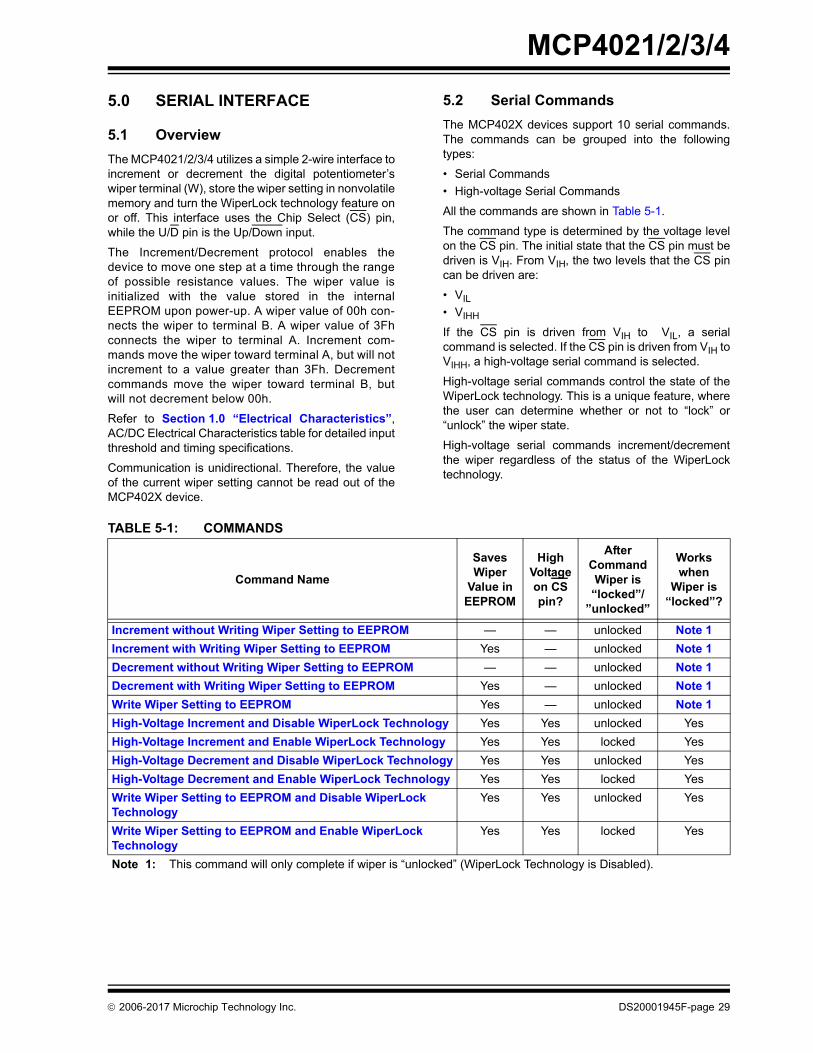
5.2 Serial Commands
The MCP402X devices support 10 serial commands.The commands can be grouped into the followingtypes:
• Serial Commands
• High-voltage Serial Commands
All the commands are shown in Table 5-1.
The command type is determined by the voltage levelon the CS pin. The initial state that the CS pin must bedriven is VIH. From VIH, the two levels that the CS pincan be driven are:
• VIL
• VIHH
If the CS pin is driven from VIH to VIL, a serialcommand is selected. If the CS pin is driven from VIH toVIHH, a high-voltage serial command is selected.
High-voltage serial commands control the state of theWiperLock technology. This is a unique feature, wherethe user can determine whether or not to “lock” or“unlock” the wiper state.
High-voltage serial commands increment/decrementthe wiper regardless of the status of the WiperLocktechnology.
TABLE 5-1: COMMANDS
Command Name
Saves Wiper
Value in EEPROM
High Voltage on CS pin?
After Command Wiper is
“locked”/”unlocked”
Works when
Wiper is “locked”?
Increment without Writing Wiper Setting to EEPROM — — unlocked Note 1
Increment with Writing Wiper Setting to EEPROM Yes — unlocked Note 1
Decrement without Writing Wiper Setting to EEPROM — — unlocked Note 1
Decrement with Writing Wiper Setting to EEPROM Yes — unlocked Note 1
Write Wiper Setting to EEPROM Yes — unlocked Note 1
High-Voltage Increment and Disable WiperLock Technology Yes Yes unlocked Yes
High-Voltage Increment and Enable WiperLock Technology Yes Yes locked Yes
High-Voltage Decrement and Disable WiperLock Technology Yes Yes unlocked Yes
High-Voltage Decrement and Enable WiperLock Technology Yes Yes locked Yes
Write Wiper Setting to EEPROM and Disable WiperLock Technology
Yes Yes unlocked Yes
Write Wiper Setting to EEPROM and Enable WiperLock Technology
Yes Yes locked Yes
Note 1: This command will only complete if wiper is “unlocked” (WiperLock Technology is Disabled).
2006-2017 Microchip Technology Inc. DS20001945F-page 29

MCP4021/2/3/4
5.2.1 INCREMENT WITHOUT WRITING WIPER SETTING TO EEPROM
This mode is achieved by initializing the U/D pin to ahigh state (VIH) prior to achieving a low state (VIL) on theCS pin. Subsequent rising edges of the U/D pinincrement the wiper setting toward terminal A. This isshown in Figure 5-1.
After the wiper is incremented to the desired position,the CS pin should be forced to VIH to ensure that“unexpected” transitions (on the U/D pin do not causethe wiper setting to increment. Driving the CS pin to VIHshould occur as soon as possible (within devicespecifications) after the last desired increment occurs.
The EEPROM value has not been updated to this newwiper value, so if the device voltage is lowered belowthe RAM retention voltage of the device, once thedevice returns to the operating range, the wiper will beloaded with the wiper setting in the EEPROM.
After the CS pin is driven to VIH (from VIL), any otherserial command may immediately be entered. This issince an EEPROM write cycle (twc) is not active.
FIGURE 5-1: Increment without Writing Wiper Setting to EEPROM.
Note: The wiper value will not overflow. That is,once the wiper value equals 0x3F,subsequent increment commands areignored.
EEPROM
U/D
CS
Wiper
1 2 3 4
WiperLock Technology
WiperLock Technology Enable
WiperLock Technology Disable
X+1X X+2 X+3 X+4
XX X X X
Note: If WiperLock technology enabled, wiper will not move.
VIH
VIH 5 6
VIL
VIL
DS20001945F-page 30 2006-2017 Microchip Technology Inc.
MCP4021/2/3/4
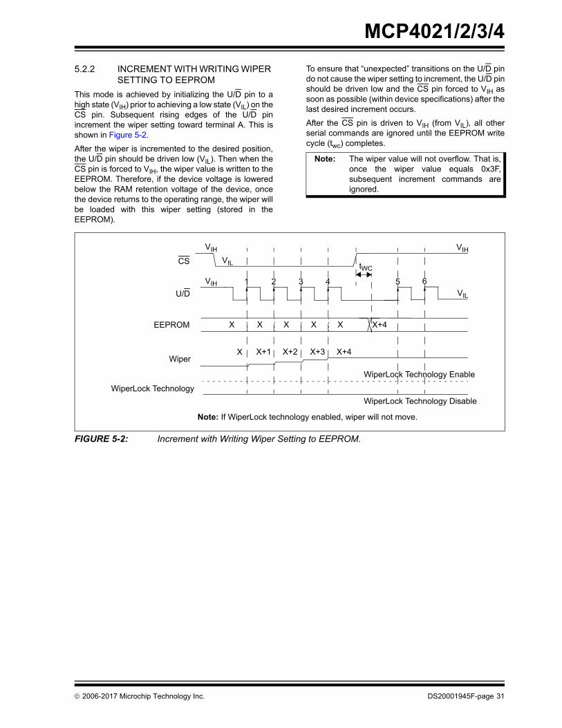
5.2.2 INCREMENT WITH WRITING WIPER SETTING TO EEPROM
This mode is achieved by initializing the U/D pin to ahigh state (VIH) prior to achieving a low state (VIL) on theCS pin. Subsequent rising edges of the U/D pinincrement the wiper setting toward terminal A. This isshown in Figure 5-2.
After the wiper is incremented to the desired position,the U/D pin should be driven low (VIL). Then when theCS pin is forced to VIH, the wiper value is written to theEEPROM. Therefore, if the device voltage is loweredbelow the RAM retention voltage of the device, oncethe device returns to the operating range, the wiper willbe loaded with this wiper setting (stored in theEEPROM).
To ensure that “unexpected” transitions on the U/D pindo not cause the wiper setting to increment, the U/D pinshould be driven low and the CS pin forced to VIH assoon as possible (within device specifications) after thelast desired increment occurs.
After the CS pin is driven to VIH (from VIL), all otherserial commands are ignored until the EEPROM writecycle (twc) completes.
FIGURE 5-2: Increment with Writing Wiper Setting to EEPROM.
Note: The wiper value will not overflow. That is,once the wiper value equals 0x3F,subsequent increment commands areignored.
EEPROM
U/D
CS
Wiper
1 2 3 4
WiperLock Technology
WiperLock Technology Enable
WiperLock Technology Disable
X+1X X+2 X+3 X+4
XX X X X X+4
Note: If WiperLock technology enabled, wiper will not move.
VIH
VIH
VIH
5 6
VIL
VIL tWC
2006-2017 Microchip Technology Inc. DS20001945F-page 31
MCP4021/2/3/4
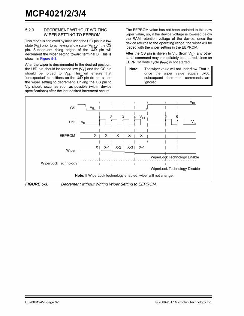
5.2.3 DECREMENT WITHOUT WRITING WIPER SETTING TO EEPROM
This mode is achieved by initializing the U/D pin to a lowstate (VIL) prior to achieving a low state (VIL) on the CSpin. Subsequent rising edges of the U/D pin willdecrement the wiper setting toward terminal B. This isshown in Figure 5-3.
After the wiper is decremented to the desired position,the U/D pin should be forced low (VIL) and the CS pinshould be forced to VIH. This will ensure that“unexpected” transitions on the U/D pin do not causethe wiper setting to decrement. Driving the CS pin toVIH should occur as soon as possible (within devicespecifications) after the last desired increment occurs.
The EEPROM value has not been updated to this newwiper value, so, if the device voltage is lowered belowthe RAM retention voltage of the device, once thedevice returns to the operating range, the wiper will beloaded with the wiper setting in the EEPROM.
After the CS pin is driven to VIH (from VIL), any otherserial command may immediately be entered, since anEEPROM write cycle (tWC) is not started.
FIGURE 5-3: Decrement without Writing Wiper Setting to EEPROM.
Note: The wiper value will not underflow. That is,once the wiper value equals 0x00,subsequent decrement commands areignored.
EEPROM
U/D
CS
Wiper
1 2 3 4
WiperLock Technology
WiperLock Technology Enable
WiperLock Technology Disable
X-1X X-2 X-3 X-4
XX X X X
Note: If WiperLock technology enabled, wiper will not change.
VIH
VIH 5 6
VIL
VIL
VIL
DS20001945F-page 32 2006-2017 Microchip Technology Inc.
MCP4021/2/3/4
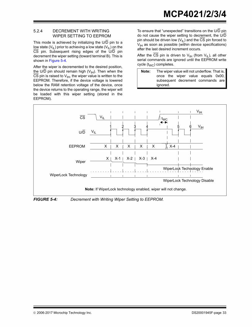
5.2.4 DECREMENT WITH WRITING WIPER SETTING TO EEPROM
This mode is achieved by initializing the U/D pin to alow state (VIL) prior to achieving a low state (VIL) on theCS pin. Subsequent rising edges of the U/D pindecrement the wiper setting (toward terminal B). This isshown in Figure 5-4.
After the wiper is decremented to the desired position,the U/D pin should remain high (VIH). Then when theCS pin is raised to VIH, the wiper value is written to theEEPROM. Therefore, if the device voltage is loweredbelow the RAM retention voltage of the device, oncethe device returns to the operating range, the wiper willbe loaded with this wiper setting (stored in theEEPROM).
To ensure that “unexpected” transitions on the U/D pindo not cause the wiper setting to decrement, the U/Dpin should be driven low (VIL) and the CS pin forced toVIH as soon as possible (within device specifications)after the last desired increment occurs.
After the CS pin is driven to VIH (from VIL), all otherserial commands are ignored until the EEPROM writecycle (tWC) completes.
FIGURE 5-4: Decrement with Writing Wiper Setting to EEPROM.
Note: The wiper value will not underflow. That is,once the wiper value equals 0x00,subsequent decrement commands areignored.
EEPROM
U/D
CS
Wiper
WiperLock Technology
WiperLock Technology Enable
WiperLock Technology Disable
X-1X X-2 X-3 X-4
XX X X X X-4
1 2 3 4
Note: If WiperLock technology enabled, wiper will not change.
VIH
VIH 5 6VIL
VIL tWC
2006-2017 Microchip Technology Inc. DS20001945F-page 33
MCP4021/2/3/4
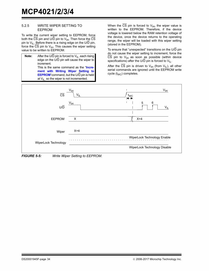
5.2.5 WRITE WIPER SETTING TO EEPROM
To write the current wiper setting to EEPROM, forceboth the CS pin and U/D pin to VIH. Then force the CSpin to VIL. Before there is a rising edge on the U/D pin,force the CS pin to VIH. This causes the wiper settingvalue to be written to EEPROM.
When the CS pin is forced to VIH, the wiper value iswritten to the EEPROM. Therefore, if the devicevoltage is lowered below the RAM retention voltage ofthe device, once the device returns to the operatingrange, the wiper will be loaded with this wiper setting(stored in the EEPROM).
To ensure that “unexpected” transitions on the U/D pindo not cause the wiper setting to increment, force theCS pin to VIH as soon as possible (within devicespecifications) after the U/D pin is forced to VIL.
After the CS pin is driven to VIH (from VIL), all otherserial commands are ignored until the EEPROM writecycle (tWC) completes.
FIGURE 5-5: Write Wiper Setting to EEPROM.
Note: After the U/D pin is forced to VIL, each risingedge on the U/D pin will cause the wiper toincrement. This is the same command as the “Incre-ment with Writing Wiper Setting toEEPROM“command, but the U/D pin is heldat VIL, so the wiper is not incremented.
EEPROM
U/D
CS
Wiper
WiperLock Technology
WiperLock Technology Enable
WiperLock Technology Disable
X+4
X X+4
VIH
VIH
VIH
5 6
VIL
VIL tWC
DS20001945F-page 34 2006-2017 Microchip Technology Inc.
MCP4021/2/3/4
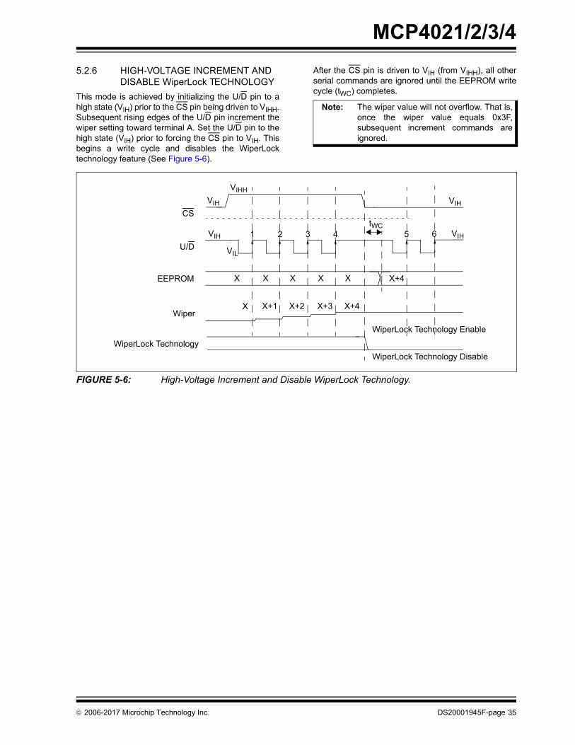
5.2.6 HIGH-VOLTAGE INCREMENT AND DISABLE WiperLock TECHNOLOGY
This mode is achieved by initializing the U/D pin to ahigh state (VIH) prior to the CS pin being driven to VIHH.Subsequent rising edges of the U/D pin increment thewiper setting toward terminal A. Set the U/D pin to thehigh state (VIH) prior to forcing the CS pin to VIH. Thisbegins a write cycle and disables the WiperLocktechnology feature (See Figure 5-6).
After the CS pin is driven to VIH (from VIHH), all otherserial commands are ignored until the EEPROM writecycle (tWC) completes.
FIGURE 5-6: High-Voltage Increment and Disable WiperLock Technology.
Note: The wiper value will not overflow. That is,once the wiper value equals 0x3F,subsequent increment commands areignored.
EEPROM
U/D
CS
Wiper
1 2 3 4
WiperLock Technology
WiperLock Technology Enable
WiperLock Technology Disable
X+1X X+2 X+3 X+4
XX X X X X+4
VIHH
VIH
VIH
VIH 5 6
VIL
VIH
tWC
2006-2017 Microchip Technology Inc. DS20001945F-page 35
MCP4021/2/3/4
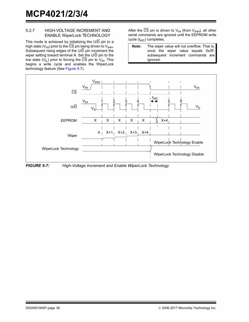
5.2.7 HIGH-VOLTAGE INCREMENT AND ENABLE WiperLock TECHNOLOGY
This mode is achieved by initializing the U/D pin to ahigh state (VIH) prior to the CS pin being driven to VIHH.Subsequent rising edges of the U/D pin increment thewiper setting toward terminal A. Set the U/D pin to thelow state (VIL) prior to forcing the CS pin to VIH. Thisbegins a write cycle and enables the WiperLocktechnology feature (See Figure 5-7).
After the CS pin is driven to VIH (from VIHH), all otherserial commands are ignored until the EEPROM writecycle (tWC) completes.
FIGURE 5-7: High-Voltage Increment and Enable WiperLock Technology.
Note: The wiper value will not overflow. That is,once the wiper value equals 0x3F,subsequent increment commands areignored.
EEPROM
U/D
CS
Wiper
1 2 3 4
WiperLock Technology
WiperLock Technology Enable
WiperLock Technology Disable
X+1X X+2 X+3 X+4
XX X X X X+4
VIHH
VIH
VIH
5 6
VIL
VIH
VIL
tWC
DS20001945F-page 36 2006-2017 Microchip Technology Inc.
MCP4021/2/3/4
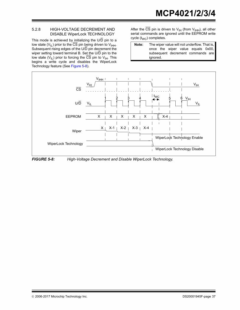
5.2.8 HIGH-VOLTAGE DECREMENT AND DISABLE WiperLock TECHNOLOGY
This mode is achieved by initializing the U/D pin to alow state (VIL) prior to the CS pin being driven to VIHH.Subsequent rising edges of the U/D pin decrement thewiper setting toward terminal B. Set the U/D pin to thelow state (VIL) prior to forcing the CS pin to VIH. Thisbegins a write cycle and disables the WiperLockTechnology feature (See Figure 5-8).
After the CS pin is driven to VIH (from VIHH), all otherserial commands are ignored until the EEPROM writecycle (tWC) completes.
FIGURE 5-8: High-Voltage Decrement and Disable WiperLock Technology.
Note: The wiper value will not underflow. That is,once the wiper value equals 0x00,subsequent decrement commands areignored.
EEPROM
U/D
CS
Wiper
1 2 3 4
WiperLock Technology
WiperLock Technology Enable
WiperLock Technology Disable
XX X X X X-4
X-1X X-2 X-3 X-4
VIHH
VIH
VIH
5 6
VIL
VIH
VIL
tWC
2006-2017 Microchip Technology Inc. DS20001945F-page 37

MCP4021/2/3/4
5.2.9 HIGH-VOLTAGE DECREMENT AND ENABLE WiperLock TECHNOLOGY
This mode is achieved by initializing the U/D pin to thelow state (VIL) prior to driving the CS pin to VIHH.Subsequent rising edges of the U/D pin decrement thewiper setting toward terminal B. Set the U/D pin to ahigh state (VIH) prior to forcing the CS pin to VIH. Thisbegins a write cycle and enables the WiperLocktechnology feature (See Figure 5-9).
After the CS pin is driven to VIH (from VIHH), all otherserial commands are ignored until the EEPROM writecycle (tWC) completes.
FIGURE 5-9: High-Voltage Decrement and Enable WiperLock Technology.
Note: The wiper value will not underflow. That is,once the wiper value equals 0x00,subsequent decrement commands areignored.
EEPROM
U/D
CS
Wiper
1 2 3 4
WiperLock Technology
WiperLock Technology Enable
WiperLock Technology Disable
XX X X X X-4
X-1X X-2 X-3 X-4
VIHH
VDD
VIH
VIH 5 6
VIH
VIL
tWC
DS20001945F-page 38 2006-2017 Microchip Technology Inc.
MCP4021/2/3/4
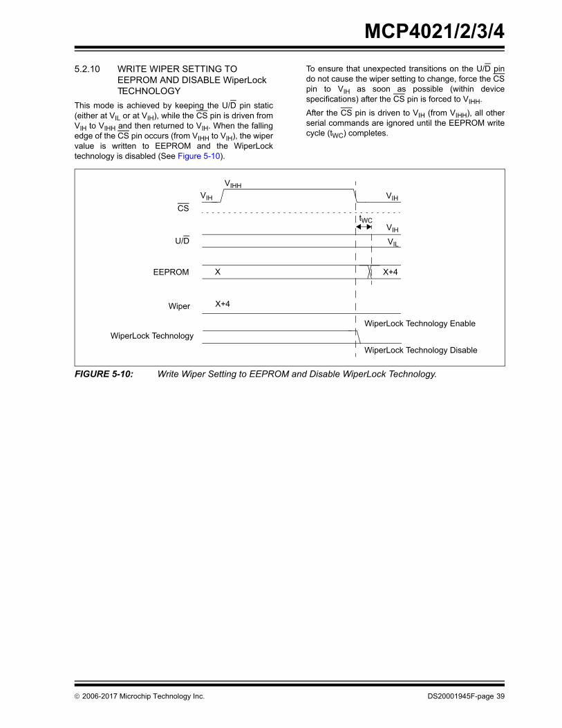
5.2.10 WRITE WIPER SETTING TO EEPROM AND DISABLE WiperLock TECHNOLOGY
This mode is achieved by keeping the U/D pin static(either at VIL or at VIH), while the CS pin is driven fromVIH to VIHH and then returned to VIH. When the fallingedge of the CS pin occurs (from VIHH to VIH), the wipervalue is written to EEPROM and the WiperLocktechnology is disabled (See Figure 5-10).
To ensure that unexpected transitions on the U/D pindo not cause the wiper setting to change, force the CSpin to VIH as soon as possible (within devicespecifications) after the CS pin is forced to VIHH.
After the CS pin is driven to VIH (from VIHH), all otherserial commands are ignored until the EEPROM writecycle (tWC) completes.
FIGURE 5-10: Write Wiper Setting to EEPROM and Disable WiperLock Technology.
EEPROM
U/D
CS
Wiper
WiperLock Technology
X+4
X X+4
WiperLock Technology Enable
WiperLock Technology Disable
VIHH
VIH
VIL
VIH VIH
tWC
2006-2017 Microchip Technology Inc. DS20001945F-page 39
MCP4021/2/3/4
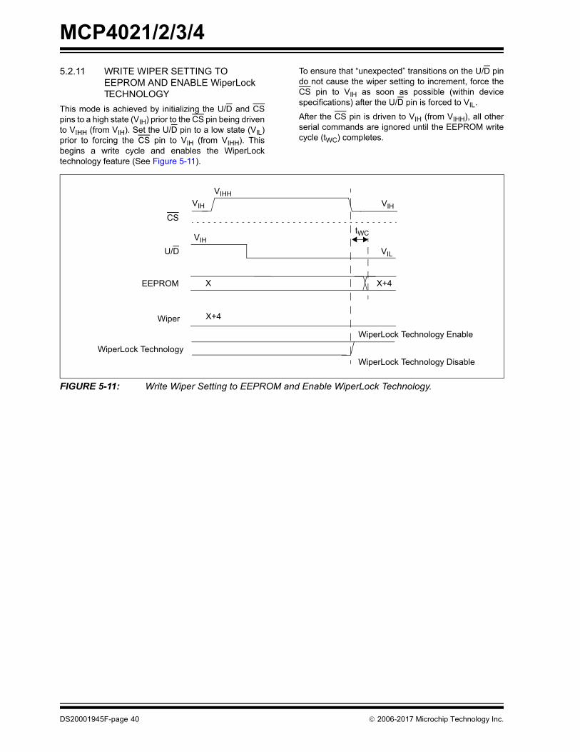
5.2.11 WRITE WIPER SETTING TO EEPROM AND ENABLE WiperLock TECHNOLOGY
This mode is achieved by initializing the U/D and CSpins to a high state (VIH) prior to the CS pin being drivento VIHH (from VIH). Set the U/D pin to a low state (VIL)prior to forcing the CS pin to VIH (from VIHH). Thisbegins a write cycle and enables the WiperLocktechnology feature (See Figure 5-11).
To ensure that “unexpected” transitions on the U/D pindo not cause the wiper setting to increment, force theCS pin to VIH as soon as possible (within devicespecifications) after the U/D pin is forced to VIL.
After the CS pin is driven to VIH (from VIHH), all otherserial commands are ignored until the EEPROM writecycle (tWC) completes.
FIGURE 5-11: Write Wiper Setting to EEPROM and Enable WiperLock Technology.
EEPROM
U/D
CS
Wiper
WiperLock Technology
X+4
X X+4
WiperLock Technology Enable
WiperLock Technology Disable
VIHH
VIH
VIH VIH
VIL
tWC
DS20001945F-page 40 2006-2017 Microchip Technology Inc.

MCP4021/2/3/4
5.3 CS High Voltage
Depending on the requirements of the system, the useof high voltage (VIHH) on the CS pin, may or may not berequired during system operation. Table 5-2 showspossible system applications, and whether a highvoltage (VIHH) is required on the system.
The MCP402X supports six high-voltage commands(the CS input voltage must meet the VIHH
specification).
TABLE 5-2: HIGH-VOLTAGE APPLICATIONS
5.3.1 TECHNIQUES TO FORCE THE CS PIN TO VIHH
The circuit in Figure 5-12 shows a method using theTC1240A doubling charge pump. When the SHDN pinis high, the TC1240A is off, and the level on the CS pinis controlled by the PIC® microcontrollers (MCUs) IO2pin.
When the SHDN pin is low, the TC1240A is on and theVOUT voltage is 2 * VDD. The resistor R1 allows the CSpin to go higher than the voltage such that the PICMCU’s IO2 pin “clamps” at approximately VDD.
FIGURE 5-12: Using the TC1240A to Generate the VIHH Voltage.
The circuit in Figure 5-13 shows the method used onthe MCP402X Nonvolatile Digital PotentiometerEvaluation Board. This method requires that thesystem voltage be approximately 5V. This ensures thatwhen the PIC10F206 enters a brown-out condition,there is an insufficient voltage level on the CS pin tochange the stored value of the wiper. The MCP402XNon-volatile Digital Potentiometer Evaluation BoardUser’s Guide (DS51546) contains a completeschematic.
GP0 is a general purpose I/O pin, while GP2 can eitherbe a general purpose I/O pin or it can output the internalclock.
For the serial commands, configure the GP2 pin as aninput (high impedance). The output state of the GP0 pinwill determine the voltage on the CS pin (VIL or VIH).
For high-voltage serial commands, force the GP0output pin to output a high level (VOH) and configure theGP2 pin to output the internal clock. This will form acharge pump and increase the voltage on the CS pin(when the system voltage is approximately 5V).
FIGURE 5-13: MCP402X Non-volatile Digital Potentiometer Evaluation Board (MCP402XEV) implementation to Generate the VIHH Voltage.
System OperationHigh
Voltage
Production calibration only - system should not update wiper setting
From Calibration
Unit
WiperLock Technology disabled during system operation
Not Required
Wiper setting can be updated and “locked” during system operation
Required
CS
PIC® MCU
MCP402X R1
IO1
IO2
C2
TC1240A VIN
SHDN
C+
C-
VOUT
C1
CS
PIC10F206
MCP402X
R1 GP0
GP2
C2 C1
2006-2017 Microchip Technology Inc. DS20001945F-page 41
MCP4021/2/3/4
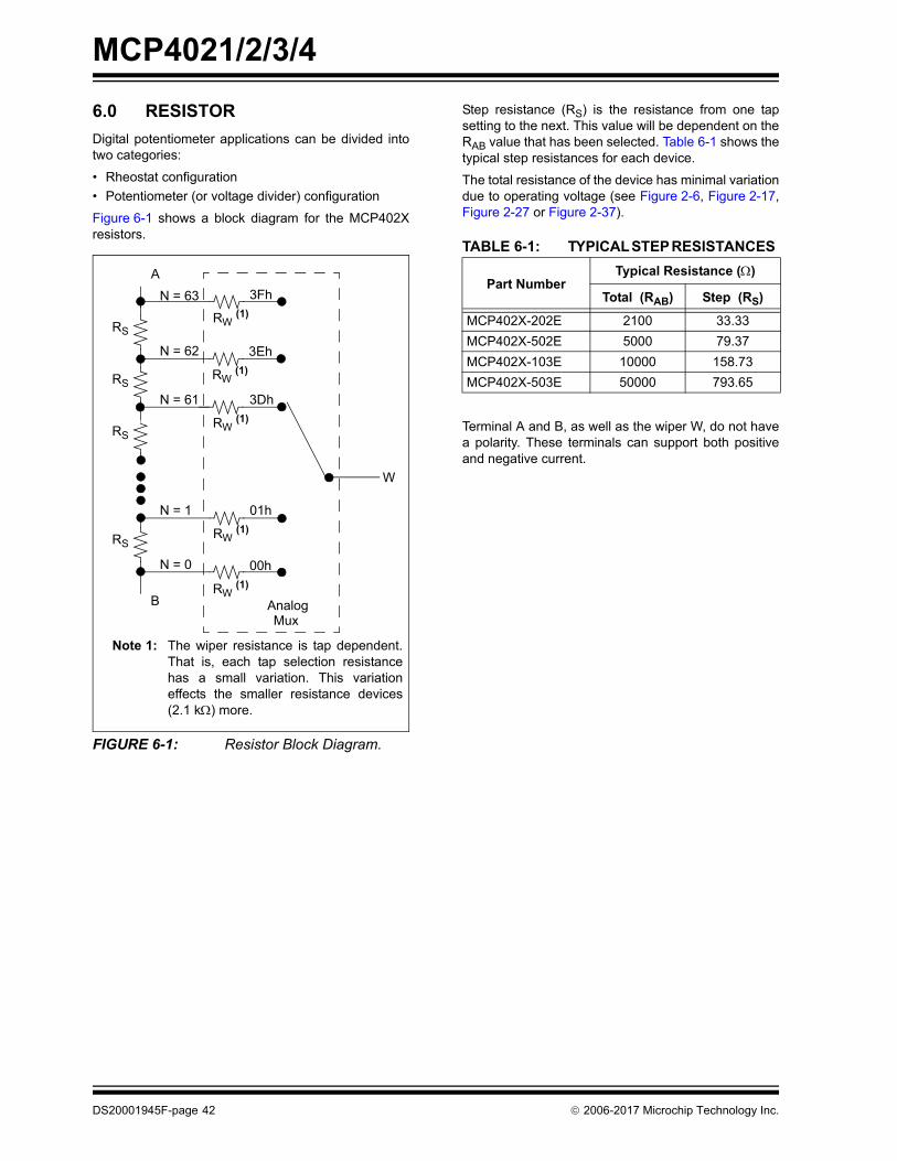
6.0 RESISTOR
Digital potentiometer applications can be divided intotwo categories:
• Rheostat configuration
• Potentiometer (or voltage divider) configuration
Figure 6-1 shows a block diagram for the MCP402Xresistors.
FIGURE 6-1: Resistor Block Diagram.
Step resistance (RS) is the resistance from one tapsetting to the next. This value will be dependent on theRAB value that has been selected. Table 6-1 shows thetypical step resistances for each device.
The total resistance of the device has minimal variationdue to operating voltage (see Figure 2-6, Figure 2-17,Figure 2-27 or Figure 2-37).
TABLE 6-1: TYPICAL STEP RESISTANCES
Terminal A and B, as well as the wiper W, do not havea polarity. These terminals can support both positiveand negative current.
RS
A
RS
RS
RS
B
N = 63
N = 62
N = 61
N = 1
N = 0
RW (1)
W
01h
AnalogMux
RW (1)
00h
RW (1)
3Dh
RW (1)
3Eh
RW (1)
3Fh
Note 1: The wiper resistance is tap dependent.That is, each tap selection resistancehas a small variation. This variationeffects the smaller resistance devices(2.1 k) more.
Part NumberTypical Resistance ()
Total (RAB) Step (RS)
MCP402X-202E 2100 33.33
MCP402X-502E 5000 79.37
MCP402X-103E 10000 158.73
MCP402X-503E 50000 793.65
DS20001945F-page 42 2006-2017 Microchip Technology Inc.

MCP4021/2/3/4
6.1 Resistor Configurations
6.1.1 RHEOSTAT CONFIGURATION
When used as a rheostat, two of the three digitalpotentiometer’s terminals are used as a resistiveelement in the circuit. With terminal W (wiper) andeither terminal A or terminal B, a variable resistor iscreated. The resistance will depend on the tap settingof the wiper and the wiper’s resistance. The resistanceis controlled by changing the wiper setting.
The unused terminal (B or A) should be left floating.Figure 6-2 shows the two possible resistors that can beused. Reversing the polarity of the A and B terminalswill not affect operation.
FIGURE 6-2: Rheostat Configuration.
This allows the control of the total resistance betweenthe two nodes. The total resistance depends on the“starting” terminal to the wiper terminal. At the code00h, the RBW resistance is minimal (RW), but the RAWresistance in maximized (RAB + RW). Conversely, at thecode 3Fh, the RAW resistance is minimal (RW), but theRBW resistance in maximized (RAB + RW).
The resistance step size (RS) equates to one LSb of theresistor.
The change in wiper-to-end terminal resistance overtemperature is shown in Figure 2-6, Figure 2-17,Figure 2-27 and Figure 2-37. The most variation overtemperature will occur in the first few codes due to thewiper resistance coefficient affecting the totalresistance. The remaining codes are dominated by thetotal resistance tempco RAB.
6.1.2 POTENTIOMETER CONFIGURATION
When used as a potentiometer, all three terminals aretied to different nodes in the circuit. This allows thepotentiometer to output a voltage proportional to theinput voltage. This configuration is sometimes calledvoltage divider mode. The potentiometer is used toprovide a variable voltage by adjusting the wiperposition between the two endpoints as shown inFigure 6-3. Reversing the polarity of the A and Bterminals will not affect operation.
FIGURE 6-3: Potentiometer Configuration.
The temperature coefficient of the RAB resistors isminimal by design. In this configuration, the resistors allchange uniformly, so minimal variation should be seen.
The wiper resistor temperature coefficient is differentfrom the RAB temperature coefficient. The voltage atnode V3 (Figure 6-3) is not dependent on this wiperresistance, just the ratio of the RAB resistors, so thistemperature coefficient in most cases can beignored.
Note: To avoid damage to the internal wipercircuitry in this configuration, care shouldbe taken to insure the current flow neverexceeds 2.5 mA.
A
B
W
Resistor
RAW RBWor
Note: To avoid damage to the internal wipercircuitry in this configuration, care shouldbe taken to insure the current flow neverexceeds 2.5 mA.
A
B
W
V1
V3
V2
2006-2017 Microchip Technology Inc. DS20001945F-page 43
MCP4021/2/3/4
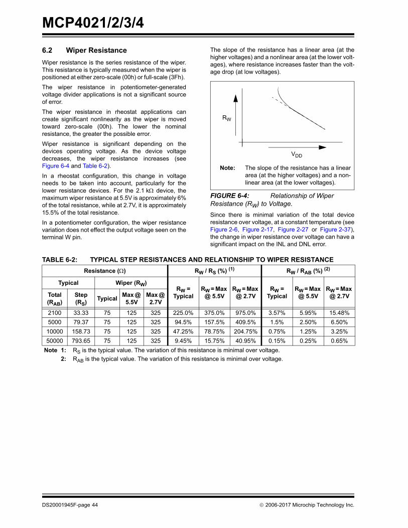
6.2 Wiper Resistance
Wiper resistance is the series resistance of the wiper.This resistance is typically measured when the wiper ispositioned at either zero-scale (00h) or full-scale (3Fh).
The wiper resistance in potentiometer-generatedvoltage divider applications is not a significant sourceof error.
The wiper resistance in rheostat applications cancreate significant nonlinearity as the wiper is movedtoward zero-scale (00h). The lower the nominalresistance, the greater the possible error.
Wiper resistance is significant depending on thedevices operating voltage. As the device voltagedecreases, the wiper resistance increases (seeFigure 6-4 and Table 6-2).
In a rheostat configuration, this change in voltageneeds to be taken into account, particularly for thelower resistance devices. For the 2.1 k device, themaximum wiper resistance at 5.5V is approximately 6%of the total resistance, while at 2.7V, it is approximately15.5% of the total resistance.
In a potentiometer configuration, the wiper resistancevariation does not effect the output voltage seen on theterminal W pin.
The slope of the resistance has a linear area (at thehigher voltages) and a nonlinear area (at the lower volt-ages), where resistance increases faster than the volt-age drop (at low voltages).
FIGURE 6-4: Relationship of Wiper Resistance (RW) to Voltage.
Since there is minimal variation of the total deviceresistance over voltage, at a constant temperature (seeFigure 2-6, Figure 2-17, Figure 2-27 or Figure 2-37),the change in wiper resistance over voltage can have asignificant impact on the INL and DNL error.
TABLE 6-2: TYPICAL STEP RESISTANCES AND RELATIONSHIP TO WIPER RESISTANCE
RW
VDD
Note: The slope of the resistance has a lineararea (at the higher voltages) and a non-linear area (at the lower voltages).
Resistance () RW / RS (%) (1) RW / RAB (%) (2)
Typical Wiper (RW) RW =
TypicalRW = Max
@ 5.5VRW = Max
@ 2.7VRW =
TypicalRW = Max
@ 5.5VRW = Max
@ 2.7VTotal (RAB)
Step (RS)
TypicalMax @
5.5VMax @
2.7V
2100 33.33 75 125 325 225.0% 375.0% 975.0% 3.57% 5.95% 15.48%
5000 79.37 75 125 325 94.5% 157.5% 409.5% 1.5% 2.50% 6.50%
10000 158.73 75 125 325 47.25% 78.75% 204.75% 0.75% 1.25% 3.25%
50000 793.65 75 125 325 9.45% 15.75% 40.95% 0.15% 0.25% 0.65%
Note 1: RS is the typical value. The variation of this resistance is minimal over voltage.
2: RAB is the typical value. The variation of this resistance is minimal over voltage.
DS20001945F-page 44 2006-2017 Microchip Technology Inc.

MCP4021/2/3/4
6.3 Operational Characteristics
Understanding the operational characteristics of thedevice’s resistor components is important to the systemdesign.
6.3.1 ACCURACY
6.3.1.1 Integral Nonlinearity (INL)
INL error for these devices is the maximum deviationbetween an actual code transition point and itscorresponding ideal transition point after offset andgain errors have been removed. These endpoints arefrom 0x00 to 0x3F. Refer to Figure 6-5.
Positive INL means higher resistance than ideal.Negative INL means lower resistance than ideal.
FIGURE 6-5: INL Accuracy.
6.3.1.2 Differential Non-Linearity (DNL)
DNL error is the measure of variations in code widthsfrom the ideal code width. A DNL error of zero wouldimply that every code is exactly 1 LSb wide.
FIGURE 6-6: DNL Accuracy.
6.3.1.3 Ratiometric Temperature Coefficient
The ratiometric temperature coefficient quantifies theerror in the ratio RAW/RWB due to temperature drift.This is typically the critical error when using apotentiometer device (MCP4021 and MCP4023) in avoltage divider configuration.
6.3.1.4 Absolute Temperature Coefficient
The absolute temperature coefficient quantifies theerror in the end-to-end resistance (nominal resistanceRAB) due to temperature drift. This is typically thecritical error when using a rheostat device (MCP4022and MCP4024) in an adjustable resistor configuration.
111
110
101
100
011
010
001
000
DigitalInputCode
ActualTransferFunction
INL < 0
Ideal TransferFunction
INL < 0
Digital Pot Output
111
110
101
100
011
010
001
000
DigitalInputCode
ActualTransferFunction
Ideal TransferFunction
Narrow Code < 1 LSb
Wide Code, > 1 LSb
Digital Pot Output
2006-2017 Microchip Technology Inc. DS20001945F-page 45

MCP4021/2/3/4
6.3.2 MONOTONIC OPERATION
Monotonic operation means that the device’sresistance increases with every step change (fromterminal A to terminal B or terminal B to terminal A).
The wiper resistance is different at each tap location.When changing from one tap position to the next (eitherincreasing or decreasing), the RW is less than theRS. When this change occurs, the device voltage andtemperature are the same for the two tap positions.
FIGURE 6-7: Resistance, RBW.
0x3F
0x3E
0x3D
0x03
0x02
0x01
0x00
Dig
ital I
npu
t Cod
e
Resistance (RBW)
RW (@ tap)
RS0
RS1
RS3
RS62
RS63
RBW = RSn + RW(@ Tap n) n = 0
n = ?
DS20001945F-page 46 2006-2017 Microchip Technology Inc.
MCP4021/2/3/4
7.0 DESIGN CONSIDERATIONS
In the design of a system with the MCP402X devices,the following considerations should be taken intoaccount:
• The power supply
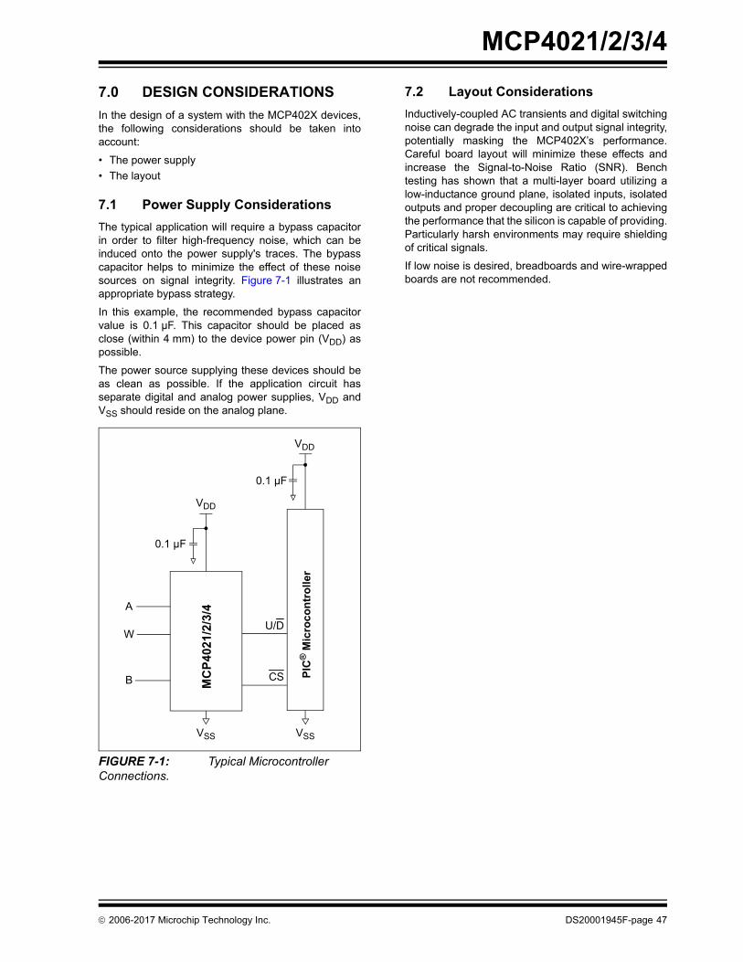
• The layout
7.1 Power Supply Considerations
The typical application will require a bypass capacitorin order to filter high-frequency noise, which can beinduced onto the power supply's traces. The bypasscapacitor helps to minimize the effect of these noisesources on signal integrity. Figure 7-1 illustrates anappropriate bypass strategy.
In this example, the recommended bypass capacitorvalue is 0.1 µF. This capacitor should be placed asclose (within 4 mm) to the device power pin (VDD) aspossible.
The power source supplying these devices should beas clean as possible. If the application circuit hasseparate digital and analog power supplies, VDD andVSS should reside on the analog plane.
FIGURE 7-1: Typical Microcontroller Connections.
7.2 Layout Considerations
Inductively-coupled AC transients and digital switchingnoise can degrade the input and output signal integrity,potentially masking the MCP402X’s performance.Careful board layout will minimize these effects andincrease the Signal-to-Noise Ratio (SNR). Benchtesting has shown that a multi-layer board utilizing alow-inductance ground plane, isolated inputs, isolatedoutputs and proper decoupling are critical to achievingthe performance that the silicon is capable of providing.Particularly harsh environments may require shieldingof critical signals.
If low noise is desired, breadboards and wire-wrappedboards are not recommended.
VDD
VDD
VSS VSS
MC
P4
021
/2/3
/4
0.1 µF
PIC
® M
icro
co
ntr
oll
er
0.1 µF
U/D
CS
W
B
A
2006-2017 Microchip Technology Inc. DS20001945F-page 47
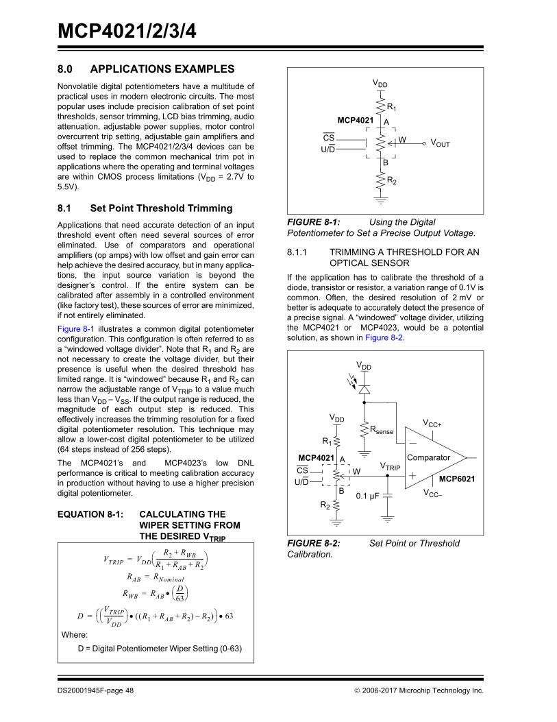
MCP4021/2/3/4
8.0 APPLICATIONS EXAMPLES
Nonvolatile digital potentiometers have a multitude ofpractical uses in modern electronic circuits. The mostpopular uses include precision calibration of set pointthresholds, sensor trimming, LCD bias trimming, audioattenuation, adjustable power supplies, motor controlovercurrent trip setting, adjustable gain amplifiers andoffset trimming. The MCP4021/2/3/4 devices can beused to replace the common mechanical trim pot inapplications where the operating and terminal voltagesare within CMOS process limitations (VDD = 2.7V to5.5V).
8.1 Set Point Threshold Trimming
Applications that need accurate detection of an inputthreshold event often need several sources of erroreliminated. Use of comparators and operationalamplifiers (op amps) with low offset and gain error canhelp achieve the desired accuracy, but in many applica-tions, the input source variation is beyond thedesigner’s control. If the entire system can becalibrated after assembly in a controlled environment(like factory test), these sources of error are minimized,if not entirely eliminated.
Figure 8-1 illustrates a common digital potentiometerconfiguration. This configuration is often referred to asa “windowed voltage divider”. Note that R1 and R2 arenot necessary to create the voltage divider, but theirpresence is useful when the desired threshold haslimited range. It is “windowed” because R1 and R2 cannarrow the adjustable range of VTRIP to a value muchless than VDD – VSS. If the output range is reduced, themagnitude of each output step is reduced. Thiseffectively increases the trimming resolution for a fixeddigital potentiometer resolution. This technique mayallow a lower-cost digital potentiometer to be utilized(64 steps instead of 256 steps).
The MCP4021’s and MCP4023’s low DNLperformance is critical to meeting calibration accuracyin production without having to use a higher precisiondigital potentiometer.
EQUATION 8-1: CALCULATING THE WIPER SETTING FROM THE DESIRED VTRIP
FIGURE 8-1: Using the Digital Potentiometer to Set a Precise Output Voltage.
8.1.1 TRIMMING A THRESHOLD FOR AN OPTICAL SENSOR
If the application has to calibrate the threshold of adiode, transistor or resistor, a variation range of 0.1V iscommon. Often, the desired resolution of 2 mV orbetter is adequate to accurately detect the presence ofa precise signal. A “windowed” voltage divider, utilizingthe MCP4021 or MCP4023, would be a potentialsolution, as shown in Figure 8-2.
FIGURE 8-2: Set Point or Threshold Calibration.VTRIP VDD
R2 RWB+
R1 RAB R2+ +----------------------------------- =
RAB RNominal=
RWB RABD63------ =
DVTRIPVDD-------------- R1 RAB R2+ + R2– 63=
Where:
D = Digital Potentiometer Wiper Setting (0-63)
VDD
VOUT
R2
A
R1
W
B
MCP4021
CS
U/D
VTRIP
0.1 µF
Comparator
VCC+
VCC–
VDD
Rsense
R1
R2
B
A
VDD
W
MCP4021
CS
U/D MCP6021
DS20001945F-page 48 2006-2017 Microchip Technology Inc.
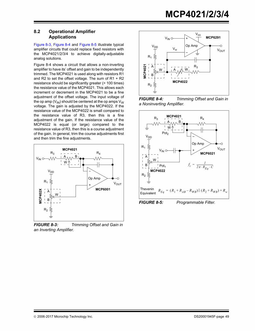
MCP4021/2/3/4
8.2 Operational Amplifier Applications
Figure 8-3, Figure 8-4 and Figure 8-5 illustrate typicalamplifier circuits that could replace fixed resistors withthe MCP4021/2/3/4 to achieve digitally-adjustableanalog solutions.
Figure 8-4 shows a circuit that allows a non-invertingamplifier to have its’ offset and gain to be independentlytrimmed. The MCP4021 is used along with resistors R1and R2 to set the offset voltage. The sum of R1 + R2resistance should be significantly greater (> 100 times)the resistance value of the MCP4021. This allows eachincrement or decrement in the MCP4021 to be a fineadjustment of the offset voltage. The input voltage ofthe op amp (VIN) should be centered at the op amps VWvoltage. The gain is adjusted by the MCP4022. If theresistance value of the MCP4022 is small compared tothe resistance value of R3, then this is a fineadjustment of the gain. If the resistance value of theMCP4022 is equal (or large) compared to theresistance value of R3, then this is a course adjustmentof the gain. In general, trim the course adjustments firstand then trim the fine adjustments.
FIGURE 8-3: Trimming Offset and Gain in an Inverting Amplifier.
FIGURE 8-4: Trimming Offset and Gain in a Noninverting Amplifier.
FIGURE 8-5: Programmable Filter.
Op Amp
VIN
VOUT
BA
W
+
–
MCP4021
R1
R2
B
A
VDD
W
R3 R4
MC
P40
2X
MCP6001
Op Amp
VIN
VOUT–
+
R1
R2
B
A
VDD
WR3
MCP6291
MC
P4
021
MCP4022
WA
VDD
VW
Op Amp
VINVOUT
BA
W
+
–
MCP4021
R1
R2
B
A
VDD
W
MCP4022
R3 R4
fc1
2 REq C -----------------------------=Pot1
Pot2
REq R1 RAB RWB–+ R2 RWB+ Rw+=TheveninEquivalent
MCP6021
2006-2017 Microchip Technology Inc. DS20001945F-page 49

MCP4021/2/3/4
8.3 Temperature Sensor Applications
Thermistors are resistors with very predictablevariation with temperature. Thermistors are a popularsensor choice when a low-cost, temperature-sensingsolution is desired. Unfortunately, thermistors havenonlinear characteristics that are undesirable, typicallyrequiring trimming in an application to achieve greateraccuracy. There are several common solutions to trimand linearize thermistors. Figure 8-6 and Figure 8-7are simple methods for linearizing a 3-terminal NTCthermistor. Both are simple voltage dividers using aPositive Temperature Coefficient (PTC) resistor (R1)with a transfer function capable of compensating for thelinearity error in the Negative Temperature Coefficient(NTC) thermistor.
The circuit, illustrated by Figure 8-6, utilizes a digitalrheostat for trimming the offset error caused by thethermistor’s part-to-part variation. This solution puts thedigital potentiometer’s RW into the voltage dividercalculation. The MCP4021/2/3/4’s RAB temperaturecoefficient is 50 ppm (-20°C to +70°C). RW’s error issubstantially greater than RAB’s error because RWvaries with VDD, wiper setting and temperature. For the50 k devices, the error introduced by RW is, in mostcases, insignificant as long as the wiper setting is > 6.For the 2 k devices, the error introduced by RW issignificant because it is a higher percentage of RWB.For these reasons, the circuit illustrated in Figure 8-6 isnot the most optimum method for “exciting” andlinearizing a thermistor.
FIGURE 8-6: Thermistor Calibration using a Digital Potentiometer in a Rheostat Configuration.
The circuit illustrated by Figure 8-7 utilizes a digitalpotentiometer for trimming the offset error. Thissolution removes RW from the trimming equation alongwith the error associated with RW. R2 is not required,but can be utilized to reduce the trimming “window” andreduce variation due to the digital potentiometer’s RABpart-to-part variability.
FIGURE 8-7: Thermistor Calibration using a Digital Potentiometer in a Potentiometer Configuration.
8.4 Wheatstone Bridge Trimming
Another common configuration to “excite” a sensor(such as a strain gauge, pressure sensor or thermistor)is the wheatstone bridge configuration. The wheat-stone bridge provides a differential output instead of asingle-ended output. Figure 8-8 illustrates awheatstone bridge utilizing one to three digitalpotentiometers. The digital potentiometers in thisexample are used to trim the offset and gain of thewheatstone bridge.
FIGURE 8-8: Wheatstone Bridge Trimming.
NTC
VDD
MCP4022
VOUT
Thermistor
R1
R2
W
A
NTC
VDD
MCP4021VOUT
Thermistor
R1
R2
VDD
MCP4022
VOUT
2.1 k
MCP402250 k
MCP402250 k
DS20001945F-page 50 2006-2017 Microchip Technology Inc.
MCP4021/2/3/4
9.0 DEVELOPMENT SUPPORT
9.1 Evaluation/Demonstration Boards
Currently there are three boards that are available thatcan be used to evaluate the MCP4021/2/3/4 family ofdevices.
1. The MCP402X Digital Potentiometer EvaluationBoard kit (MCP402XEV) contains a simpledemonstration board utilizing a PIC10F206, theMCP4021 and a blank PCB, which can bepopulated with any desired MCP4021/2/3/4device in a SOT-23-5, SOT-23-6 or 150 milSOIC 8-pin package.
This board has two push buttons to control whenthe PIC® microcontroller generates MCP402Xserial commands. The example firmwaredemonstrates the following commands:
• Increment
• Decrement
• High-Voltage Increment and Enable WiperLock Technology
• High-Voltage Decrement and Enable WiperLock Technology
• High-Voltage Increment and Disable WiperLock Technology
• High-Voltage Decrement and Disable WiperLock Technology
The populated board (with the MCP4021) canbe used to evaluate the other MCP402X devicesby appropriately jumpering the PCB pads.
2. The SOT-23-5/6 Evaluation Board (VSUPEV2)can be used to evaluate the characteristics ofthe MCP4022, MCP4023 and MCP4024devices.
3. The 8-pin SOIC/MSOP/TSSOP/DIP EvaluationBoard (SOIC8EV) can be used to evaluate thecharacteristics of the MCP4021 device in eitherthe SOIC or MSOP package.
4. The MCP4XXX Digital Potentiometer DaughterBoard allows the system designer to quicklyevaluate the operation of Microchip Technol-ogy's MCP42XXX and MCP402X Digital Poten-tiometers. The board supports two MCP42XXXdevices and an MCP402X device, which can bereplaced with an MCP401X device.
The board also has a voltage doubler device(TC1240A), which can be used to show theWiperLock Technology feature of the MCP4021.
These boards may be purchased directly from theMicrochip web site at www.microchip.com.
2006-2017 Microchip Technology Inc. DS20001945F-page 51
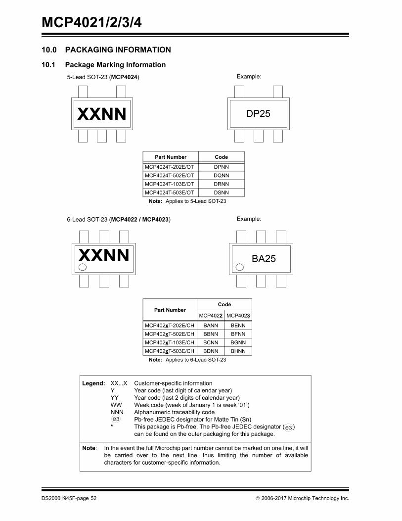
MCP4021/2/3/4
10.0 PACKAGING INFORMATION
10.1 Package Marking Information
5-Lead SOT-23 (MCP4024) Example:
Part Number Code
MCP4024T-202E/OT DPNN
MCP4024T-502E/OT DQNN
MCP4024T-103E/OT DRNN
MCP4024T-503E/OT DSNN
Note: Applies to 5-Lead SOT-23
6-Lead SOT-23 (MCP4022 / MCP4023) Example:
Part NumberCode
MCP4022 MCP4023
MCP402xT-202E/CH BANN BENN
MCP402xT-502E/CH BBNN BFNN
MCP402xT-103E/CH BCNN BGNN
MCP402xT-503E/CH BDNN BHNN
Note: Applies to 6-Lead SOT-23
Legend: XX...X Customer-specific informationY Year code (last digit of calendar year)YY Year code (last 2 digits of calendar year)WW Week code (week of January 1 is week ‘01’)NNN Alphanumeric traceability code Pb-free JEDEC designator for Matte Tin (Sn)* This package is Pb-free. The Pb-free JEDEC designator ( )
can be found on the outer packaging for this package.
Note: In the event the full Microchip part number cannot be marked on one line, it willbe carried over to the next line, thus limiting the number of availablecharacters for customer-specific information.
3e
3e
XXNN DP25
XXNN BA25
DS20001945F-page 52 2006-2017 Microchip Technology Inc.

MCP4021/2/3/4
Package Marking Information
8-Lead MSOP (MCP4021)
Example:
Example:8-Lead DFN (2x3) (MCP4021)
8-Lead SOIC (150 mil) (MCP4021) Example:
Part Number Code
MCP4021T-202E/MC AAA
MCP4021T-502E/MC AAB
MCP4021T-103E/MC AAC
MCP4021T-503E/MC AAD
Note: Applies to 8-Lead DFN
Part NumbersCode
8L-MSOP 8L-SOIC
MCP4021-202E/MS MCP4021-202E/SN 22
MCP4021-502E/MS MCP4021-502E/SN 52
MCP4021-103E/MS MCP4021-103E/SN 13
MCP4021-503E/MS MCP4021-503E/SN 53
AAA64025
402122
640256
NNN
402153E
SN^^ 1640
256
3e
8-Lead MSOP (MCP4021)
2006-2017 Microchip Technology Inc. DS20001945F-page 53

MCP4021/2/3/4
0.15 C D2X
NOTE 1 1 2
N
TOP VIEW
SIDE VIEW
Microchip Technology Drawing C04-028D [OT] Sheet 1 of
For the most current package drawings, please see the Microchip Packaging Specification located athttp://www.microchip.com/packaging
Note:
0.20 C
C
SEATING PLANE
A A2
A1
e
NX bB0.20 C A-B D
e1
D
E1
E1/2
E/2
E
DA
0.20 C 2X
(DATUM D)(DATUM A-B)
A
ASEE SHEET 2
5-Lead Plastic Small Outline Transistor (OT) [SOT23]
DS20001945F-page 54 2006-2017 Microchip Technology Inc.
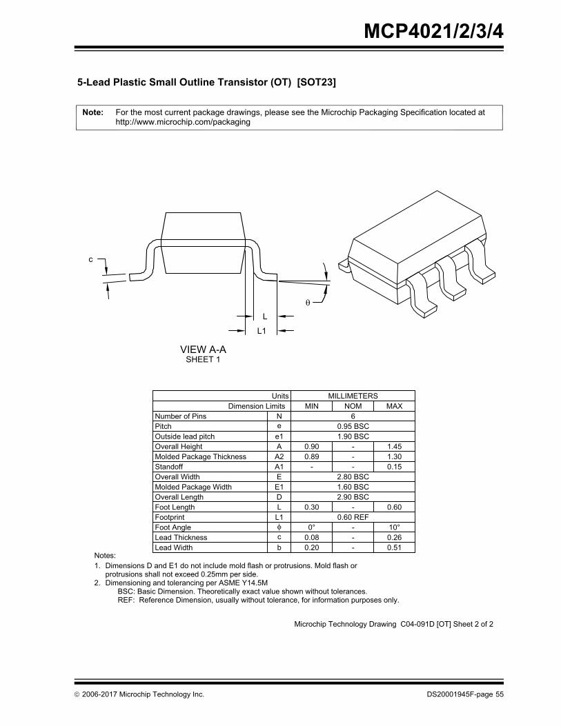
MCP4021/2/3/4
Microchip Technology Drawing C04-091D [OT] Sheet 2 of
For the most current package drawings, please see the Microchip Packaging Specification located athttp://www.microchip.com/packaging
Note:
c
L
L1
VIEW A-ASHEET 1
5-Lead Plastic Small Outline Transistor (OT) [SOT23]
protrusions shall not exceed 0.25mm per side.1.
BSC: Basic Dimension. Theoretically exact value shown without tolerances.2.
Foot Angle
Number of PinsPitchOutside lead pitchOverall HeightMolded Package ThicknessStandoffOverall WidthMolded Package WidthOverall LengthFoot LengthFootprint
Lead ThicknessLead Width
Notes:
L1
bc
Dimension Limits
EE1DL
e1AA2A1
Units
Ne
0°0.080.20 -
--
10°0.260.51
MILLIMETERS
0.95 BSC1.90 BSC
0.30
0.900.89
-
0.60 REF
2.90 BSC-
2.80 BSC1.60 BSC
--
-
MIN6
NOM
1.451.300.15
0.60
MAX
REF: Reference Dimension, usually without tolerance, for information purposes only.
Dimensions D and E1 do not include mold flash or protrusions. Mold flash or
Dimensioning and tolerancing per ASME Y14.5M
2006-2017 Microchip Technology Inc. DS20001945F-page 55

MCP4021/2/3/4
RECOMMENDED LAND PATTERN
5-Lead Plastic Small Outline Transistor (OT) [SOT23]
For the most current package drawings, please see the Microchip Packaging Specification located athttp://www.microchip.com/packaging
Note:
BSC: Basic Dimension. Theoretically exact value shown without tolerances.
Notes:1. Dimensioning and tolerancing per ASME Y14.5M
Microchip Technology Drawing No. C04-2091A [OT]
Dimension Limits
Contact Pad Length (X5)
Overall Width
Distance Between Pads
Contact Pad Width (X5)
Contact PitchContact Pad Spacing
3.90
1.10G
Z
Y1.70
0.60
MAXMIN
CX
E
UnitsNOM
0.95 BSC2.80
MILLIMETERS
Distance Between Pads GX 0.35
1
5
X
Y
Z C
E
GX
G
2
SILK SCREEN
DS20001945F-page 56 2006-2017 Microchip Technology Inc.
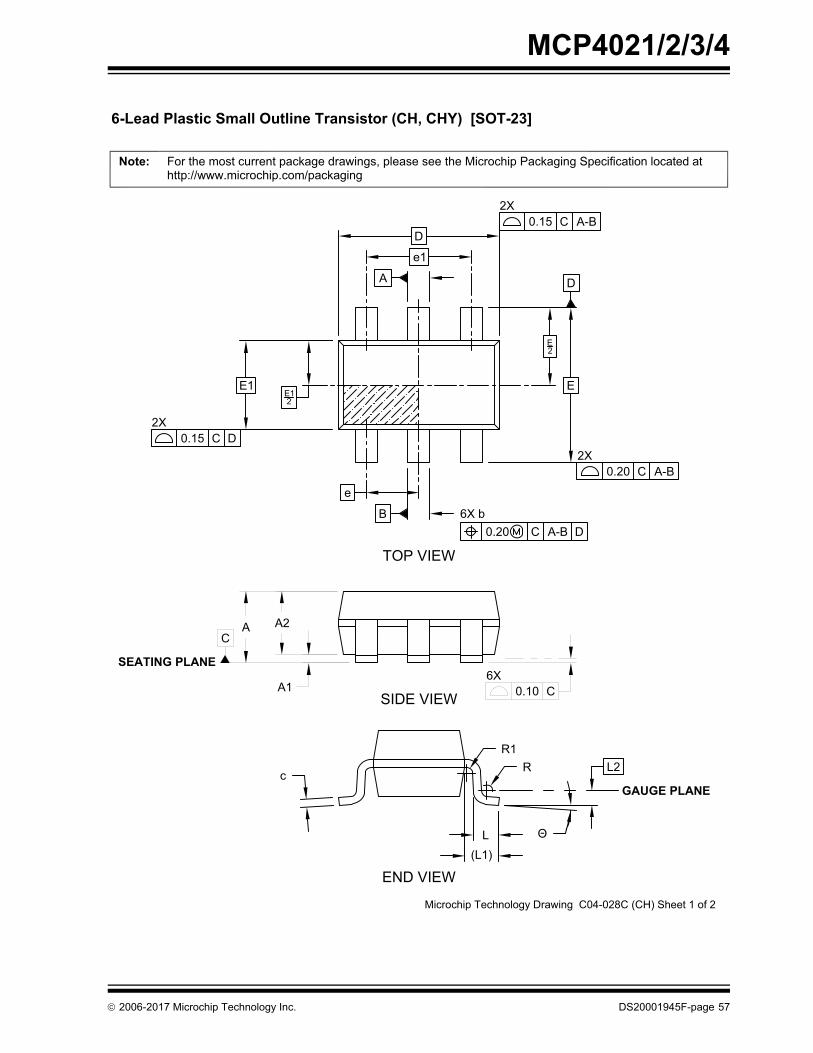
MCP4021/2/3/4
B
A
0.15 C A-B
0.15 C D
0.20 C A-B D
2X
TOP VIEW
SIDE VIEW
END VIEW
0.10 C
Microchip Technology Drawing C04-028C (CH) Sheet 1 of 2
2X
6X
For the most current package drawings, please see the Microchip Packaging Specification located athttp://www.microchip.com/packaging
Note:
6-Lead Plastic Small Outline Transistor (CH, CHY) [SOT-23]
D
EE1
e
e1
6X b
E2
E12
D
A A2
A1
L2
L(L1)
RR1
c
0.20 C A-B2X
C
SEATING PLANE
GAUGE PLANE
2006-2017 Microchip Technology Inc. DS20001945F-page 57
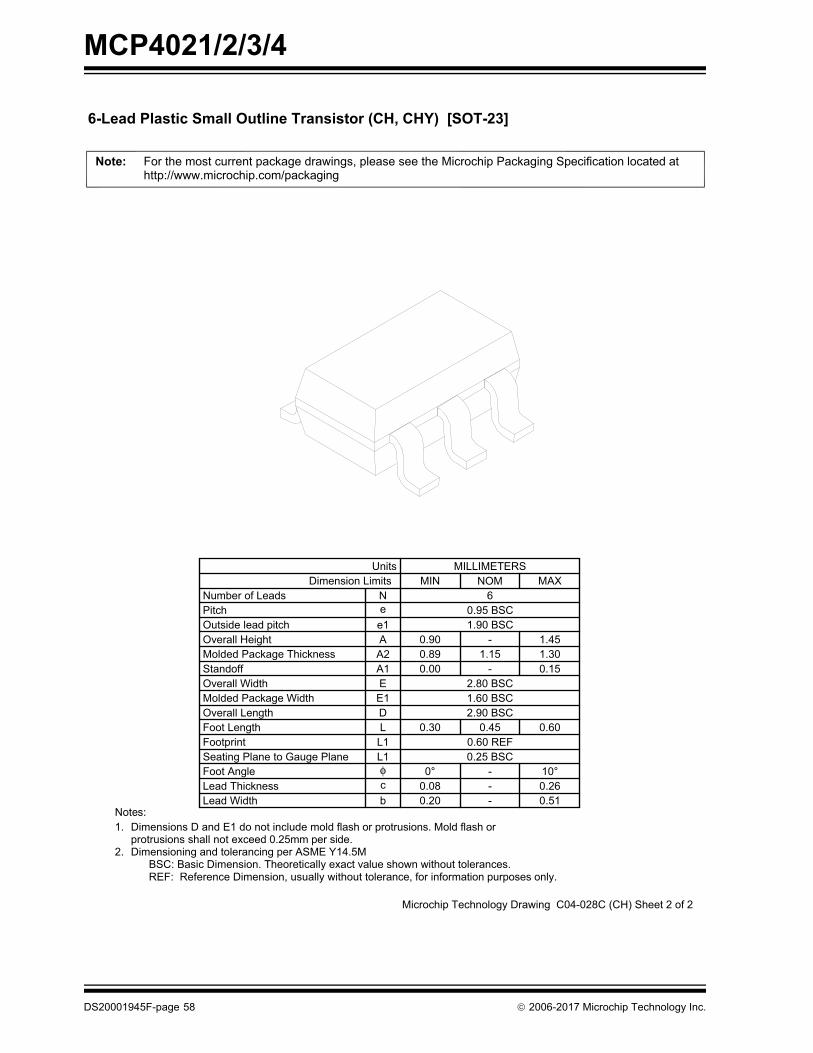
MCP4021/2/3/4
Microchip Technology Drawing C04-028C (CH) Sheet 2 of 2
6-Lead Plastic Small Outline Transistor (CH, CHY) [SOT-23]
For the most current package drawings, please see the Microchip Packaging Specification located athttp://www.microchip.com/packaging
Note:
protrusions shall not exceed 0.25mm per side.1.
BSC: Basic Dimension. Theoretically exact value shown without tolerances.2.
Notes:
REF: Reference Dimension, usually without tolerance, for information purposes only.
Dimensions D and E1 do not include mold flash or protrusions. Mold flash or
Dimensioning and tolerancing per ASME Y14.5M
Foot Angle
Number of LeadsPitchOutside lead pitchOverall HeightMolded Package ThicknessStandoffOverall WidthMolded Package WidthOverall LengthFoot LengthFootprint
Lead ThicknessLead Width
L1
φ
bc
Dimension Limits
EE1DL
e1AA2A1
Units
Ne
0°0.080.20 -
--
10°0.260.51
MILLIMETERS
0.95 BSC1.90 BSC
0.30
0.900.890.00
0.60 REF
2.90 BSC0.45
2.80 BSC1.60 BSC
1.15-
-
MIN6
NOM
1.451.300.15
0.60
MAX
Seating Plane to Gauge Plane L1 0.25 BSC
DS20001945F-page 58 2006-2017 Microchip Technology Inc.
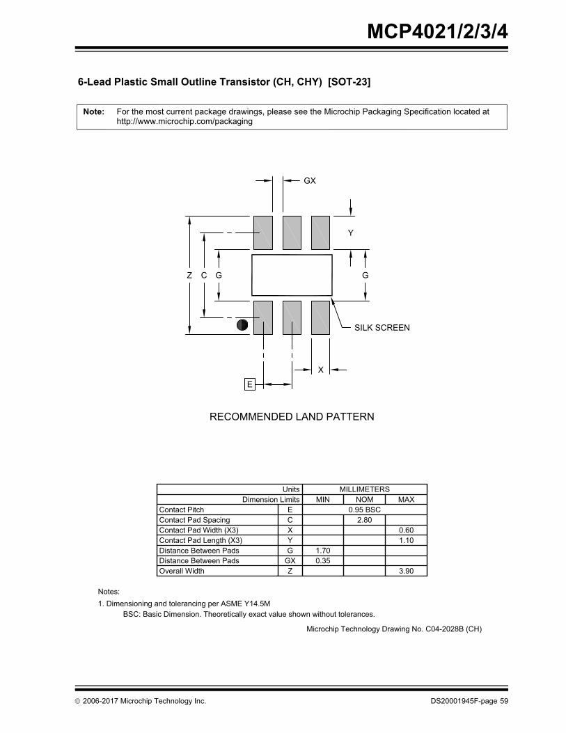
MCP4021/2/3/4
RECOMMENDED LAND PATTERN
Microchip Technology Drawing No. C04-2028B (CH)
6-Lead Plastic Small Outline Transistor (CH, CHY) [SOT-23]
For the most current package drawings, please see the Microchip Packaging Specification located athttp://www.microchip.com/packaging
Note:
BSC: Basic Dimension. Theoretically exact value shown without tolerances.
Notes:1. Dimensioning and tolerancing per ASME Y14.5M
Dimension Limits
Contact Pad Length (X3)
Overall Width
Distance Between Pads
Contact Pad Width (X3)
Contact PitchContact Pad Spacing
3.90
1.10G
Z
Y1.70
0.60
MAXMIN
CX
E
UnitsNOM
0.95 BSC2.80
MILLIMETERS
Distance Between Pads GX 0.35
E
X
GX
Y
GCZ
SILK SCREEN
G
2006-2017 Microchip Technology Inc. DS20001945F-page 59
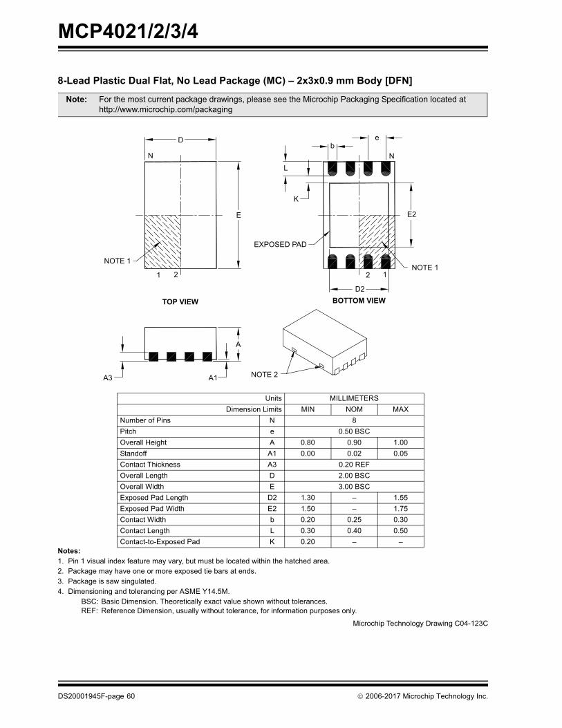
MCP4021/2/3/4
���������� �������������������������������������� !�""�#��$�%���&
�����'�� ��������!"�����# $�% �&"� �'�������*�+"&�'"!&�+ �����& #�3�&����&� ���&�� #��� ���� ���7�� �'������ ��� ����'�� � $�! #�&� �+��!��&� �#!�9� ���7�� ��!�!�3�!���"��& #��� ��' �!���������#�&�� �������� �����;�<���=��
>�?@ >�!�����' �!������� �� &������� $��&����" �!��3��3�&��"&�&�� ���� !��;G@ � % � �� ���' �!���*�"!"�����3�&��"&�&�� ���� *�%�����%��'�&����"��! !������
����' G���&� �'�!&��"�� �&���7�� �#��3���!*�� �! �! �&� �������������7������� ��%���&��������& #��&��&&@JJ333�'����������'J��7�����
K��&! ��QQ��;�;����' �!����Q�'�&! ��U UY� ��Z
U"'+ ���%����! U [��&�� ��=��>�?Y� �����\ ���& � ��[� ���� �����&��#�%%� �� ���� ���� ���=?��&��&�����7� !! �9 ������;GY� �����Q ��&� � �����>�?Y� �����]�#&� ; 9����>�?;$�! #���#�Q ��&� �� ��9� ^ ��==;$�! #���#�]�#&� ;� ��=� ^ ���=?��&��&�]�#&� + ���� ���= ��9�?��&��&�Q ��&� Q ��9� ���� ��=�?��&��&&�;$�! #���# _ ���� ^ ^
D
N
E
NOTE 1
1 2
EXPOSED PAD
NOTE 12 1
D2
K
L
E2
N
eb
A3 A1
A
NOTE 2
BOTTOM VIEWTOP VIEW
�������� � �������� ���3��� ?����9?
DS20001945F-page 60 2006-2017 Microchip Technology Inc.

MCP4021/2/3/4
Note: For the most current package drawings, please see the Microchip Packaging Specification located at http://www.microchip.com/packaging
2006-2017 Microchip Technology Inc. DS20001945F-page 61

MCP4021/2/3/4
Note: For the most current package drawings, please see the Microchip Packaging Specification located at http://www.microchip.com/packaging
DS20001945F-page 62 2006-2017 Microchip Technology Inc.
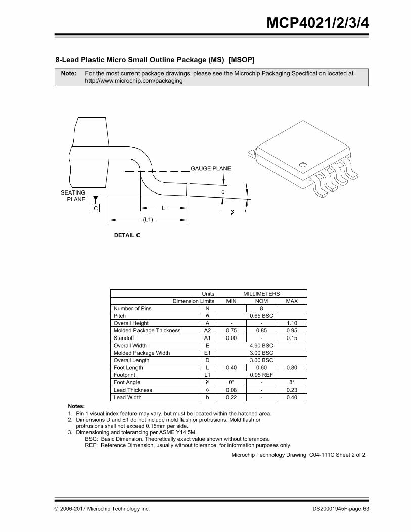
MCP4021/2/3/4
Note: For the most current package drawings, please see the Microchip Packaging Specification located at http://www.microchip.com/packaging
2006-2017 Microchip Technology Inc. DS20001945F-page 63

MCP4021/2/3/4
Note: For the most current package drawings, please see the Microchip Packaging Specification located at http://www.microchip.com/packaging
DS20001945F-page 64 2006-2017 Microchip Technology Inc.

MCP4021/2/3/4
0.25 C A–B D
CSEATING
PLANE
TOP VIEW
SIDE VIEW
VIEW A–A
0.10 C
0.10 C
Microchip Technology Drawing No. C04-057-SN Rev D Sheet 1 of 2
8X
For the most current package drawings, please see the Microchip Packaging Specification located athttp://www.microchip.com/packaging
Note:
8-Lead Plastic Small Outline (SN) - Narrow, 3.90 mm (.150 In.) Body [SOIC]
1 2
N
h
h
A1
A2A
A
B
e
D
E
E2
E12
E1
NOTE 5
NOTE 5
NX b
0.10 C A–B2X
H 0.23
(L1)L
R0.13
R0.13
VIEW C
SEE VIEW C
NOTE 1
D
2006-2017 Microchip Technology Inc. DS20001945F-page 65
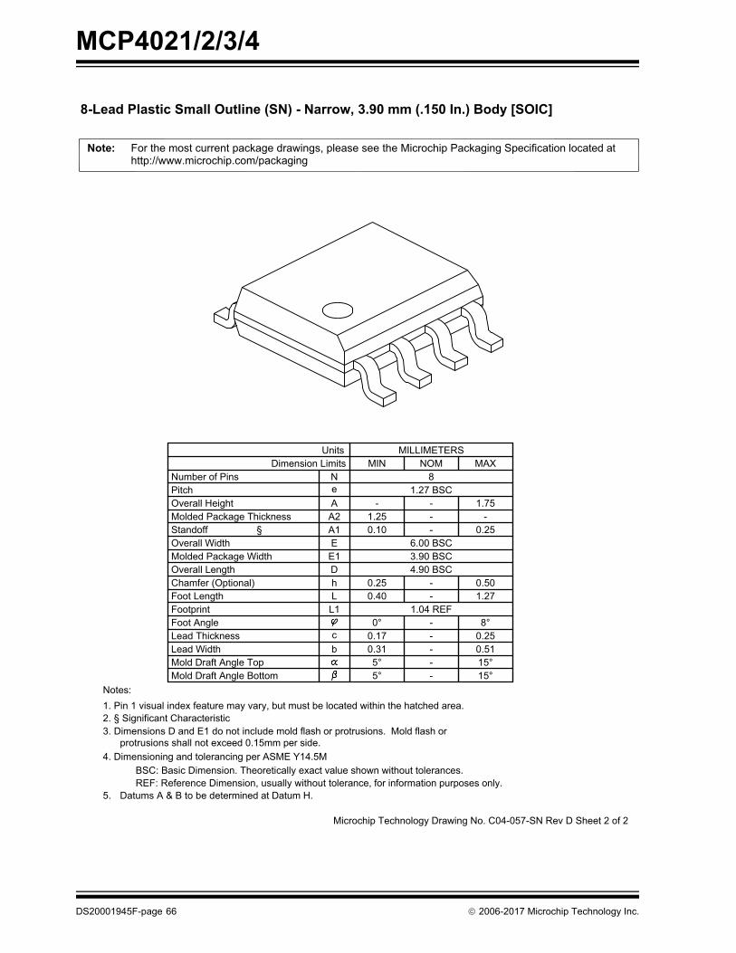
MCP4021/2/3/4
Microchip Technology Drawing No. C04-057-SN Rev D Sheet 2 of 2
8-Lead Plastic Small Outline (SN) - Narrow, 3.90 mm (.150 In.) Body [SOIC]
For the most current package drawings, please see the Microchip Packaging Specification located athttp://www.microchip.com/packaging
Note:
Foot Angle 0° - 8°
15°-5°Mold Draft Angle Bottom15°-5°Mold Draft Angle Top0.51-0.31bLead Width0.25-0.17cLead Thickness
1.27-0.40LFoot Length0.50-0.25hChamfer (Optional)
4.90 BSCDOverall Length3.90 BSCE1Molded Package Width6.00 BSCEOverall Width
0.25-0.10A1Standoff--1.25A2Molded Package Thickness
1.75--AOverall Height1.27 BSCePitch
8NNumber of PinsMAXNOMMINDimension Limits
MILLIMETERSUnits
protrusions shall not exceed 0.15mm per side.3. Dimensions D and E1 do not include mold flash or protrusions. Mold flash or
REF: Reference Dimension, usually without tolerance, for information purposes only.BSC: Basic Dimension. Theoretically exact value shown without tolerances.
1. Pin 1 visual index feature may vary, but must be located within the hatched area.2. § Significant Characteristic
4. Dimensioning and tolerancing per ASME Y14.5M
Notes:
§
Footprint L1 1.04 REF
5. Datums A & B to be determined at Datum H.
DS20001945F-page 66 2006-2017 Microchip Technology Inc.

MCP4021/2/3/4
RECOMMENDED LAND PATTERN
Microchip Technology Drawing C04-2057-SN Rev B
8-Lead Plastic Small Outline (SN) - Narrow, 3.90 mm Body [SOIC]
BSC: Basic Dimension. Theoretically exact value shown without tolerances.
Notes:Dimensioning and tolerancing per ASME Y14.5M1.
For the most current package drawings, please see the Microchip Packaging Specification located athttp://www.microchip.com/packaging
Note:
Dimension LimitsUnits
CContact Pad SpacingContact Pitch
MILLIMETERS
1.27 BSCMIN
EMAX
5.40
Contact Pad Length (X8)Contact Pad Width (X8)
Y1X1
1.550.60
NOM
E
X1
C
Y1
SILK SCREEN
2006-2017 Microchip Technology Inc. DS20001945F-page 67

MCP4021/2/3/4
NOTES:
DS20001945F-page 68 2006-2017 Microchip Technology Inc.
MCP4021/2/3/4
APPENDIX A: REVISION HISTORY
Revision F (December 2017)
The following is the list of modifications:
1. Updated the High-Voltage Input Entry Voltageentry in the “AC/DC Characteristics” table.
2. Updated Table 6-1 “Typical Step Resistances”.
Revision E (December 2006)
The following is the list of modifications:
1. Added device designators in conditions columnto associate units (MHz) in Bandwidth –3 dBparameter in the table “AC/DC Characteris-tics” table.
2. Added device designations in conditions columnfor R-INL and R-DNL specifications.
3. Added disclaimers to package outline drawings.
Revision D (October 2006)
The following is the list of modifications:
1. Changed the EEPROM write cycle time (TWC)from a maximum of 5 ms to a maximum of10 ms (overvoltage and temperature) with a typ-ical of 5 ms.
2. For the 10 k device, the rheostat differentialnonlinearity specification at 2.7V was changedfrom ±0.5 LSb to ±1.0 LSb.
3. Figure 2-9 in Section 2.0 “Typical Perfor-mance Curves” was updated with the correctdata.
4. Added Figure 2-48 for –3 db Bandwidthinformation.
5. Updated available Development Tools.
6. Added disclaimer to package outline drawings.
Revision C (November 2005)
The following is the list of modifications:
1. Enhanced Descriptions.
2. Reordered Sections.
3. Added 8-lead MSOP and DFN packages.
Revision B (April 2005)
The following is the list of modifications:
1. Updated part numbers in Product IdentifcationSection (PIS).
2. Added Appendix A: Revision History.
Revision A (April 2005)
• Original release of this document.
2006-2017 Microchip Technology Inc. DS20001945F-page 69
MCP4021/2/3/4
NOTES:
DS20001945F-page 70 2006-2017 Microchip Technology Inc.
MCP4021/2/3/4
PRODUCT IDENTIFICATION SYSTEM
To order or obtain information, e.g., on pricing or delivery, refer to the factory or the listed sales office.
Device: MCP4021: Single Potentiometer with U/D InterfaceMCP4021T: Single Potentiometer with U/D Interface
(Tape and Reel) (SOIC, MSOP)MCP4022: Single Rheostat with U/D interfaceMCP4022T: Single Rheostat with U/D interface
(Tape and Reel) (SOT-23-6)MCP4023: Single Potentiometer to GND with U/D
InterfaceMCP4023T: Single Potentiometer to GND with U/D
Interface (Tape and Reel) (SOT-23-6)MCP4024: Single Rheostat to GND with U/D
InterfaceMCP4024T: Single Rheostat to GND with U/D
Interface (Tape and Reel)(SOT-23-5)
Resistance Version: 202 = 2.1 k502 = 5 k103 = 10 k503 = 50 k
Temperature Range: E = -40°C to +125°C
Package: CH = Plastic Small Outline Transistor, 6-lead MC = Plastic Dual Flat No Lead (2x3x0.9 mm), 8-leadMS = Plastic MSOP, 8-leadSN = Plastic SOIC, (150 mil Body), 8-leadOT = Plastic Small Outline Transistor, 5-lead
PART NO. X /XX
PackageTemperatureRange
Device
Examples:
a) MCP4021-103E/MS: 10 k, 8-LD MSOPb) MCP4021-103E/SN: 10 k, 8-LD SOICc) MCP4021T-103E/MC: T/R, 10 k, 8-LD DFNd) MCP4021T-103E/MS: T/R, 10 k, 8-LD MSOPe) MCP4021T-103E/SN: T/R, 10 k, 8-LD SOICf) MCP4021-202E/MS: 2.1 k, 8-LD MSOPg) MCP4021-202E/SN: 2.1 k, 8-LD SOICh) MCP4021T-202E/MC: T/R, 2.1 k, 8-LD DFNi) MCP4021T-202E/MS: T/R, 2.1 k, 8-LD MSOPj) MCP4021T-202E/SN: T/R, 2.1 k, 8-LD SOICk) MCP4021-502E/MS: 5 k, 8-LD MSOPl) MCP4021-502E/SN: 5 k, 8-LD SOICm) MCP4021T-502E/MC: T/R, 5 k, 8-LD DFNn) MCP4021T-502E/MS: T/R, 5 k, 8-LD MSOPo) MCP4021T-502E/SN: T/R, 5 k, 8-LD SOICp) MCP4021-503E/MS: 50 k, 8-LD MSOPq) MCP4021-503E/SN: 50 k, 8-LD SOICr) MCP4021T-503E/MC: T/R, 50 k, 8-LD DFNs) MCP4021T-503E/MS: T/R, 50 k, 8-LD MSOPt) MCP4021T-503E/SN: T/R, 50 k, 8-LD SOIC
a) MCP4022T-202E/CH 2.1 k, 6-LD SOT-23b) MCP4022T-502E/CH 5 k, 6-LD SOT-23c) MCP4022T-103E/CH 10 k, 6-LD SOT-23d) MCP4022T-503E/CH 50 k, 6-LD SOT-23
a) MCP4023T-202E/CH 2.1 k, 6-LD SOT-23b) MCP4023T-502E/CH 5 k, 6-LD SOT-23c) MCP4023T-103E/CH 10 k, 6-LD SOT-23d) MCP4023T-503E/CH 50 k, 6-LD SOT-23
a) MCP4024T-202E/OT 2.1 k, 5-LD SOT-23b) MCP4024T-502E/OT 5 k, 5-LD SOT-23c) MCP4024T-103E/OT 10 k, 5-LD SOT-23d) MCP4024T-503E/OT 50 k, 5-LD SOT-23
XXX
ResistanceVersion
2006-2017 Microchip Technology Inc. DS20001945F-page 71

MCP4021/2/3/4
NOTES:
DS20001945F-page 72 2006-2017 Microchip Technology Inc.
Note the following details of the code protection feature on Microchip devices:
• Microchip products meet the specification contained in their particular Microchip Data Sheet.
• Microchip believes that its family of products is one of the most secure families of its kind on the market today, when used in the intended manner and under normal conditions.
• There are dishonest and possibly illegal methods used to breach the code protection feature. All of these methods, to our knowledge, require using the Microchip products in a manner outside the operating specifications contained in Microchip’s Data Sheets. Most likely, the person doing so is engaged in theft of intellectual property.
• Microchip is willing to work with the customer who is concerned about the integrity of their code.
• Neither Microchip nor any other semiconductor manufacturer can guarantee the security of their code. Code protection does not mean that we are guaranteeing the product as “unbreakable.”
Code protection is constantly evolving. We at Microchip are committed to continuously improving the code protection features of ourproducts. Attempts to break Microchip’s code protection feature may be a violation of the Digital Millennium Copyright Act. If such actsallow unauthorized access to your software or other copyrighted work, you may have a right to sue for relief under that Act.
Information contained in this publication regarding deviceapplications and the like is provided only for your convenienceand may be superseded by updates. It is your responsibility toensure that your application meets with your specifications.MICROCHIP MAKES NO REPRESENTATIONS ORWARRANTIES OF ANY KIND WHETHER EXPRESS ORIMPLIED, WRITTEN OR ORAL, STATUTORY OROTHERWISE, RELATED TO THE INFORMATION,INCLUDING BUT NOT LIMITED TO ITS CONDITION,QUALITY, PERFORMANCE, MERCHANTABILITY ORFITNESS FOR PURPOSE. Microchip disclaims all liabilityarising from this information and its use. Use of Microchipdevices in life support and/or safety applications is entirely atthe buyer’s risk, and the buyer agrees to defend, indemnify andhold harmless Microchip from any and all damages, claims,suits, or expenses resulting from such use. No licenses areconveyed, implicitly or otherwise, under any Microchipintellectual property rights unless otherwise stated.
2006-2017 Microchip Technology Inc.
Microchip received ISO/TS-16949:2009 certification for its worldwide headquarters, design and wafer fabrication facilities in Chandler and Tempe, Arizona; Gresham, Oregon and design centers in California and India. The Company’s quality system processes and procedures are for its PIC® MCUs and dsPIC® DSCs, KEELOQ® code hopping devices, Serial EEPROMs, microperipherals, nonvolatile memory and analog products. In addition, Microchip’s quality system for the design and manufacture of development systems is ISO 9001:2000 certified.
QUALITYMANAGEMENTSYSTEMCERTIFIEDBYDNV
== ISO/TS16949==
Trademarks
The Microchip name and logo, the Microchip logo, AnyRate, AVR, AVR logo, AVR Freaks, BeaconThings, BitCloud, CryptoMemory, CryptoRF, dsPIC, FlashFlex, flexPWR, Heldo, JukeBlox, KEELOQ, KEELOQ logo, Kleer, LANCheck, LINK MD, maXStylus, maXTouch, MediaLB, megaAVR, MOST, MOST logo, MPLAB, OptoLyzer, PIC, picoPower, PICSTART, PIC32 logo, Prochip Designer, QTouch, RightTouch, SAM-BA, SpyNIC, SST, SST Logo, SuperFlash, tinyAVR, UNI/O, and XMEGA are registered trademarks of Microchip Technology Incorporated in the U.S.A. and other countries.
ClockWorks, The Embedded Control Solutions Company, EtherSynch, Hyper Speed Control, HyperLight Load, IntelliMOS, mTouch, Precision Edge, and Quiet-Wire are registered trademarks of Microchip Technology Incorporated in the U.S.A.
Adjacent Key Suppression, AKS, Analog-for-the-Digital Age, Any Capacitor, AnyIn, AnyOut, BodyCom, chipKIT, chipKIT logo, CodeGuard, CryptoAuthentication, CryptoCompanion, CryptoController, dsPICDEM, dsPICDEM.net, Dynamic Average Matching, DAM, ECAN, EtherGREEN, In-Circuit Serial Programming, ICSP, Inter-Chip Connectivity, JitterBlocker, KleerNet, KleerNet logo, Mindi, MiWi, motorBench, MPASM, MPF, MPLAB Certified logo, MPLIB, MPLINK, MultiTRAK, NetDetach, Omniscient Code Generation, PICDEM, PICDEM.net, PICkit, PICtail, PureSilicon, QMatrix, RightTouch logo, REAL ICE, Ripple Blocker, SAM-ICE, Serial Quad I/O, SMART-I.S., SQI, SuperSwitcher, SuperSwitcher II, Total Endurance, TSHARC, USBCheck, VariSense, ViewSpan, WiperLock, Wireless DNA, and ZENA are trademarks of Microchip Technology Incorporated in the U.S.A. and other countries.
SQTP is a service mark of Microchip Technology Incorporated in the U.S.A.
Silicon Storage Technology is a registered trademark of Microchip Technology Inc. in other countries.
GestIC is a registered trademark of Microchip Technology Germany II GmbH & Co. KG, a subsidiary of Microchip Technology Inc., in other countries.
All other trademarks mentioned herein are property of their respective companies.
© 2017, Microchip Technology Incorporated, All Rights Reserved.
ISBN: 978-1-5224-2436-9
DS20001945F-page 73
DS20001945F-page 74 2006-2017 Microchip Technology Inc.
AMERICASCorporate Office2355 West Chandler Blvd.Chandler, AZ 85224-6199Tel: 480-792-7200 Fax: 480-792-7277Technical Support: http://www.microchip.com/supportWeb Address: www.microchip.com
AtlantaDuluth, GA Tel: 678-957-9614 Fax: 678-957-1455
Austin, TXTel: 512-257-3370
BostonWestborough, MA Tel: 774-760-0087 Fax: 774-760-0088
ChicagoItasca, IL Tel: 630-285-0071 Fax: 630-285-0075
DallasAddison, TX Tel: 972-818-7423 Fax: 972-818-2924
DetroitNovi, MI Tel: 248-848-4000
Houston, TX Tel: 281-894-5983
IndianapolisNoblesville, IN Tel: 317-773-8323Fax: 317-773-5453Tel: 317-536-2380
Los AngelesMission Viejo, CA Tel: 949-462-9523Fax: 949-462-9608Tel: 951-273-7800
Raleigh, NC Tel: 919-844-7510
New York, NY Tel: 631-435-6000
San Jose, CA Tel: 408-735-9110Tel: 408-436-4270
Canada - TorontoTel: 905-695-1980 Fax: 905-695-2078
ASIA/PACIFICAustralia - SydneyTel: 61-2-9868-6733
China - BeijingTel: 86-10-8569-7000
China - ChengduTel: 86-28-8665-5511
China - ChongqingTel: 86-23-8980-9588
China - DongguanTel: 86-769-8702-9880
China - GuangzhouTel: 86-20-8755-8029
China - HangzhouTel: 86-571-8792-8115
China - Hong Kong SARTel: 852-2943-5100
China - NanjingTel: 86-25-8473-2460
China - QingdaoTel: 86-532-8502-7355
China - ShanghaiTel: 86-21-3326-8000
China - ShenyangTel: 86-24-2334-2829
China - ShenzhenTel: 86-755-8864-2200
China - SuzhouTel: 86-186-6233-1526
China - WuhanTel: 86-27-5980-5300
China - XianTel: 86-29-8833-7252
China - XiamenTel: 86-592-2388138
China - ZhuhaiTel: 86-756-3210040
ASIA/PACIFICIndia - BangaloreTel: 91-80-3090-4444
India - New DelhiTel: 91-11-4160-8631
India - PuneTel: 91-20-4121-0141
Japan - OsakaTel: 81-6-6152-7160
Japan - TokyoTel: 81-3-6880- 3770
Korea - DaeguTel: 82-53-744-4301
Korea - SeoulTel: 82-2-554-7200
Malaysia - Kuala LumpurTel: 60-3-7651-7906
Malaysia - PenangTel: 60-4-227-8870
Philippines - ManilaTel: 63-2-634-9065
SingaporeTel: 65-6334-8870
Taiwan - Hsin ChuTel: 886-3-577-8366
Taiwan - KaohsiungTel: 886-7-213-7830
Taiwan - TaipeiTel: 886-2-2508-8600
Thailand - BangkokTel: 66-2-694-1351
Vietnam - Ho Chi MinhTel: 84-28-5448-2100
EUROPEAustria - WelsTel: 43-7242-2244-39Fax: 43-7242-2244-393
Denmark - CopenhagenTel: 45-4450-2828 Fax: 45-4485-2829
Finland - EspooTel: 358-9-4520-820
France - ParisTel: 33-1-69-53-63-20 Fax: 33-1-69-30-90-79
Germany - GarchingTel: 49-8931-9700
Germany - HaanTel: 49-2129-3766400
Germany - HeilbronnTel: 49-7131-67-3636
Germany - KarlsruheTel: 49-721-625370
Germany - MunichTel: 49-89-627-144-0 Fax: 49-89-627-144-44
Germany - RosenheimTel: 49-8031-354-560
Israel - Ra’anana Tel: 972-9-744-7705
Italy - Milan Tel: 39-0331-742611 Fax: 39-0331-466781
Italy - PadovaTel: 39-049-7625286
Netherlands - DrunenTel: 31-416-690399 Fax: 31-416-690340
Norway - TrondheimTel: 47-7289-7561
Poland - WarsawTel: 48-22-3325737
Romania - BucharestTel: 40-21-407-87-50
Spain - MadridTel: 34-91-708-08-90Fax: 34-91-708-08-91
Sweden - GothenbergTel: 46-31-704-60-40
Sweden - StockholmTel: 46-8-5090-4654
UK - WokinghamTel: 44-118-921-5800Fax: 44-118-921-5820
Worldwide Sales and Service
10/25/17