mc33816, sd6 programmable solenoid controller for ... · pdf file3 pin connections ... contact...
TRANSCRIPT

Document Number: MC33816 Rev. 8.0, 4/2018
NXP SemiconductorsData Sheet: Advance Information
SD6 programmable solenoid controller for precision solenoid control applicationsThe 33816 is a SMARTMOS programmable gate driver IC for precision solenoid control applications. The IC consists of five external MOSFET high-side pre-drivers and seven external MOSFET low-side pre-drivers. The 33816 provides a flexible solution for MOSFET’s gate drive with a versatile control and optimized latency time. Gate drive, diagnosis, and protection are managed through four independent microcores, and two Code RAM and two Data RAM banks.The IC contains two internal voltage regulators with overvoltage and undervoltage monitoring and protection. There are four current sense modules and VDS monitoring for fault detection and annunciation via a serial peripheral interface (SPI).The device includes both individual charge pump outputs for each high-side pre-drivers and a high-voltage DC-DC converter low-side pre-driver.These features along with cost effective packaging, make the 33816 ideal for powertrain engine control applications.Features• Battery voltage range, 5.0 V < VBATT < 32 V• Pre-drive operating voltage up to 72 V• High-side/ low-side pre-drive PWM capability up to 100 kHz–30 nC• All pre-drivers have four selectable slew rates• Eight selectable, pre-defined VDS monitoring thresholds• Encryption for microcode protection• Integrated 1.0 MHz back-up clock
Figure 1. MC33816 simplified application diagram
SOLENOID CONTROLLER
33816
AE SUFFIX (PB-FREE)98ASA00237D64-PIN LQFP
EXPOSED PAD
Applications• Automotive (12 V), truck and industrial (24 V)
powertrain• Diesel and gasoline direct injection• Transmission
VBATT
VCC5
MOSI
SCLK
CSB
MISO
START1
START6
FLAG0
DRVEN
IRQB
B_HS1
G_HS1
S_HS1
B_HS5
G_HS5
S_HS5
VSENSEP1
G_LS7
VBOOST
MOSI
SCLK
MISO
GPIO
MCU
33816
CSB
ETPU
FLAG2
ETPU
VBAT
VCCIO
VCC2P5
VCCP
5.0 V
CLK
GPIO
GPIO RESETB
OA_1ADC
OA_2ADC
G_LS1
D_LS1
VSENSEN1
VSENSEP3
VSENSEN3
VSENSEP4
VSENSEN4
VBAT
VBOOST
G_LS6
D_LS6
VBAT/VBOOST
GPIO
GPIO
GPIO
Load
* This document contains certain information on a new product.Specifications and information herein are subject to change without notice.
© NXP B.V. 2018

Table of Contents
1 Orderable parts . . . . . . . . . . . . . . . . . . . . . . . . . . . . . . . . . . . . . . . . . . . . . . . . . . . . . . . . . . . . . . . . . . . . . . . . . . . . . . . . . . . . . . . . 4
1.1 Cipher Key . . . . . . . . . . . . . . . . . . . . . . . . . . . . . . . . . . . . . . . . . . . . . . . . . . . . . . . . . . . . . . . . . . . . . . . . . . . . . . . . . . . . . . . 4
2 Internal block diagram . . . . . . . . . . . . . . . . . . . . . . . . . . . . . . . . . . . . . . . . . . . . . . . . . . . . . . . . . . . . . . . . . . . . . . . . . . . . . . . . . . . 5
2.1 Simplified internal diagram . . . . . . . . . . . . . . . . . . . . . . . . . . . . . . . . . . . . . . . . . . . . . . . . . . . . . . . . . . . . . . . . . . . . . . . . . . . 5
3 Pin connections . . . . . . . . . . . . . . . . . . . . . . . . . . . . . . . . . . . . . . . . . . . . . . . . . . . . . . . . . . . . . . . . . . . . . . . . . . . . . . . . . . . . . . . . 6
3.1 Pinout diagram . . . . . . . . . . . . . . . . . . . . . . . . . . . . . . . . . . . . . . . . . . . . . . . . . . . . . . . . . . . . . . . . . . . . . . . . . . . . . . . . . . . . 6
3.2 Pin definitions . . . . . . . . . . . . . . . . . . . . . . . . . . . . . . . . . . . . . . . . . . . . . . . . . . . . . . . . . . . . . . . . . . . . . . . . . . . . . . . . . . . . . 6
4 General product characteristics . . . . . . . . . . . . . . . . . . . . . . . . . . . . . . . . . . . . . . . . . . . . . . . . . . . . . . . . . . . . . . . . . . . . . . . . . . . . 9
4.1 Maximum ratings . . . . . . . . . . . . . . . . . . . . . . . . . . . . . . . . . . . . . . . . . . . . . . . . . . . . . . . . . . . . . . . . . . . . . . . . . . . . . . . . . . 9
4.2 Thermal characteristics . . . . . . . . . . . . . . . . . . . . . . . . . . . . . . . . . . . . . . . . . . . . . . . . . . . . . . . . . . . . . . . . . . . . . . . . . . . . 11
4.3 Operating conditions . . . . . . . . . . . . . . . . . . . . . . . . . . . . . . . . . . . . . . . . . . . . . . . . . . . . . . . . . . . . . . . . . . . . . . . . . . . . . . 12
4.4 Supply currents . . . . . . . . . . . . . . . . . . . . . . . . . . . . . . . . . . . . . . . . . . . . . . . . . . . . . . . . . . . . . . . . . . . . . . . . . . . . . . . . . . 13
5 General description . . . . . . . . . . . . . . . . . . . . . . . . . . . . . . . . . . . . . . . . . . . . . . . . . . . . . . . . . . . . . . . . . . . . . . . . . . . . . . . . . . . . 14
5.1 Introduction . . . . . . . . . . . . . . . . . . . . . . . . . . . . . . . . . . . . . . . . . . . . . . . . . . . . . . . . . . . . . . . . . . . . . . . . . . . . . . . . . . . . . 14
5.2 Features . . . . . . . . . . . . . . . . . . . . . . . . . . . . . . . . . . . . . . . . . . . . . . . . . . . . . . . . . . . . . . . . . . . . . . . . . . . . . . . . . . . . . . . . 14
5.3 Block diagram . . . . . . . . . . . . . . . . . . . . . . . . . . . . . . . . . . . . . . . . . . . . . . . . . . . . . . . . . . . . . . . . . . . . . . . . . . . . . . . . . . . 15
5.4 Functional description . . . . . . . . . . . . . . . . . . . . . . . . . . . . . . . . . . . . . . . . . . . . . . . . . . . . . . . . . . . . . . . . . . . . . . . . . . . . . 15
6 Functional block description . . . . . . . . . . . . . . . . . . . . . . . . . . . . . . . . . . . . . . . . . . . . . . . . . . . . . . . . . . . . . . . . . . . . . . . . . . . . . 16
6.1 Power up/down sequence . . . . . . . . . . . . . . . . . . . . . . . . . . . . . . . . . . . . . . . . . . . . . . . . . . . . . . . . . . . . . . . . . . . . . . . . . . 16
6.2 Power supplies and monitoring . . . . . . . . . . . . . . . . . . . . . . . . . . . . . . . . . . . . . . . . . . . . . . . . . . . . . . . . . . . . . . . . . . . . . . 17
6.3 High-side pre-drivers . . . . . . . . . . . . . . . . . . . . . . . . . . . . . . . . . . . . . . . . . . . . . . . . . . . . . . . . . . . . . . . . . . . . . . . . . . . . . . 33
6.4 Low-side pre-drivers (LS1 - LS6) . . . . . . . . . . . . . . . . . . . . . . . . . . . . . . . . . . . . . . . . . . . . . . . . . . . . . . . . . . . . . . . . . . . . . 41
6.5 VDS and VSRC monitor and load biasing . . . . . . . . . . . . . . . . . . . . . . . . . . . . . . . . . . . . . . . . . . . . . . . . . . . . . . . . . . . . . . 45
6.6 Current measurement . . . . . . . . . . . . . . . . . . . . . . . . . . . . . . . . . . . . . . . . . . . . . . . . . . . . . . . . . . . . . . . . . . . . . . . . . . . . . 52
6.7 Current measurement for DC-DC conversion . . . . . . . . . . . . . . . . . . . . . . . . . . . . . . . . . . . . . . . . . . . . . . . . . . . . . . . . . . . 60
6.8 OA_x output pin and multiplexer . . . . . . . . . . . . . . . . . . . . . . . . . . . . . . . . . . . . . . . . . . . . . . . . . . . . . . . . . . . . . . . . . . . . . 63
6.9 PLL and backup clock . . . . . . . . . . . . . . . . . . . . . . . . . . . . . . . . . . . . . . . . . . . . . . . . . . . . . . . . . . . . . . . . . . . . . . . . . . . . . 67
6.10 Digital I/Os . . . . . . . . . . . . . . . . . . . . . . . . . . . . . . . . . . . . . . . . . . . . . . . . . . . . . . . . . . . . . . . . . . . . . . . . . . . . . . . . . . . . . . 69
6.11 SPI interface . . . . . . . . . . . . . . . . . . . . . . . . . . . . . . . . . . . . . . . . . . . . . . . . . . . . . . . . . . . . . . . . . . . . . . . . . . . . . . . . . . . . . 71
6.12 Internal pull-up and pull-down . . . . . . . . . . . . . . . . . . . . . . . . . . . . . . . . . . . . . . . . . . . . . . . . . . . . . . . . . . . . . . . . . . . . . . . 75
6.15 Device logic block description . . . . . . . . . . . . . . . . . . . . . . . . . . . . . . . . . . . . . . . . . . . . . . . . . . . . . . . . . . . . . . . . . . . . . . . 81
7 CPU features and operation . . . . . . . . . . . . . . . . . . . . . . . . . . . . . . . . . . . . . . . . . . . . . . . . . . . . . . . . . . . . . . . . . . . . . . . . . . . . 160
7.1 Introduction . . . . . . . . . . . . . . . . . . . . . . . . . . . . . . . . . . . . . . . . . . . . . . . . . . . . . . . . . . . . . . . . . . . . . . . . . . . . . . . . . . . . 160
7.2 Features . . . . . . . . . . . . . . . . . . . . . . . . . . . . . . . . . . . . . . . . . . . . . . . . . . . . . . . . . . . . . . . . . . . . . . . . . . . . . . . . . . . . . . . 160
7.3 Symbols and notation . . . . . . . . . . . . . . . . . . . . . . . . . . . . . . . . . . . . . . . . . . . . . . . . . . . . . . . . . . . . . . . . . . . . . . . . . . . . . 161
8 CPU features and operation overview . . . . . . . . . . . . . . . . . . . . . . . . . . . . . . . . . . . . . . . . . . . . . . . . . . . . . . . . . . . . . . . . . . . . . 164
8.1 Introduction . . . . . . . . . . . . . . . . . . . . . . . . . . . . . . . . . . . . . . . . . . . . . . . . . . . . . . . . . . . . . . . . . . . . . . . . . . . . . . . . . . . . 164
8.2 Memory and signals management programming model . . . . . . . . . . . . . . . . . . . . . . . . . . . . . . . . . . . . . . . . . . . . . . . . . . 164
8.3 Addressing modes . . . . . . . . . . . . . . . . . . . . . . . . . . . . . . . . . . . . . . . . . . . . . . . . . . . . . . . . . . . . . . . . . . . . . . . . . . . . . . . 168
NXP Semiconductors 2
33816

9 Instruction set overview . . . . . . . . . . . . . . . . . . . . . . . . . . . . . . . . . . . . . . . . . . . . . . . . . . . . . . . . . . . . . . . . . . . . . . . . . . . . . . . . 170
9.1 Introduction . . . . . . . . . . . . . . . . . . . . . . . . . . . . . . . . . . . . . . . . . . . . . . . . . . . . . . . . . . . . . . . . . . . . . . . . . . . . . . . . . . . . . 170
9.2 Instruction set description . . . . . . . . . . . . . . . . . . . . . . . . . . . . . . . . . . . . . . . . . . . . . . . . . . . . . . . . . . . . . . . . . . . . . . . . . . 170
9.3 Arithmetic logic unit (ALU) instructions . . . . . . . . . . . . . . . . . . . . . . . . . . . . . . . . . . . . . . . . . . . . . . . . . . . . . . . . . . . . . . . . 172
9.4 Configuration instructions . . . . . . . . . . . . . . . . . . . . . . . . . . . . . . . . . . . . . . . . . . . . . . . . . . . . . . . . . . . . . . . . . . . . . . . . . . 174
9.5 Digital control . . . . . . . . . . . . . . . . . . . . . . . . . . . . . . . . . . . . . . . . . . . . . . . . . . . . . . . . . . . . . . . . . . . . . . . . . . . . . . . . . . . 177
9.6 Diagnosis Instructions . . . . . . . . . . . . . . . . . . . . . . . . . . . . . . . . . . . . . . . . . . . . . . . . . . . . . . . . . . . . . . . . . . . . . . . . . . . . 179
9.7 Flow control instructions . . . . . . . . . . . . . . . . . . . . . . . . . . . . . . . . . . . . . . . . . . . . . . . . . . . . . . . . . . . . . . . . . . . . . . . . . . . 179
9.8 Load instructions . . . . . . . . . . . . . . . . . . . . . . . . . . . . . . . . . . . . . . . . . . . . . . . . . . . . . . . . . . . . . . . . . . . . . . . . . . . . . . . . 181
10 Instruction glossary . . . . . . . . . . . . . . . . . . . . . . . . . . . . . . . . . . . . . . . . . . . . . . . . . . . . . . . . . . . . . . . . . . . . . . . . . . . . . . . . . . . 182
10.1 Introduction . . . . . . . . . . . . . . . . . . . . . . . . . . . . . . . . . . . . . . . . . . . . . . . . . . . . . . . . . . . . . . . . . . . . . . . . . . . . . . . . . . . . . 182
10.2 Glossary information . . . . . . . . . . . . . . . . . . . . . . . . . . . . . . . . . . . . . . . . . . . . . . . . . . . . . . . . . . . . . . . . . . . . . . . . . . . . . . 182
10.3 Operand subsets . . . . . . . . . . . . . . . . . . . . . . . . . . . . . . . . . . . . . . . . . . . . . . . . . . . . . . . . . . . . . . . . . . . . . . . . . . . . . . . . 183
10.4 Glossary . . . . . . . . . . . . . . . . . . . . . . . . . . . . . . . . . . . . . . . . . . . . . . . . . . . . . . . . . . . . . . . . . . . . . . . . . . . . . . . . . . . . . . . 185
11 Packaging . . . . . . . . . . . . . . . . . . . . . . . . . . . . . . . . . . . . . . . . . . . . . . . . . . . . . . . . . . . . . . . . . . . . . . . . . . . . . . . . . . . . . . . . . . . 297
11.1 Package mechanical dimensions . . . . . . . . . . . . . . . . . . . . . . . . . . . . . . . . . . . . . . . . . . . . . . . . . . . . . . . . . . . . . . . . . . . . 297
12 Revision history . . . . . . . . . . . . . . . . . . . . . . . . . . . . . . . . . . . . . . . . . . . . . . . . . . . . . . . . . . . . . . . . . . . . . . . . . . . . . . . . . . . . . . 301
3 NXP Semiconductors
33816

1 Orderable parts
This section describes the part numbers available to be purchased along with their differences. Valid orderable part numbers are provided on the web. To determine the orderable part numbers for this device, go to http://www.nxp.com and perform a part number search for the following device numbers.
1.1 Cipher Key
Contact a NXP sales representative to obtain devices with a specific encryption key and the associated code encryptor.
Table 1. Orderable part variations
Part number (1) Temperature (TA) Package
MC33816AE -40 °C to 125 °C LQFP 64-pin exposed pad
Notes1. To order parts in Tape & Reel, add the R2 suffix to the part number.
NXP Semiconductors 4
33816

2 Internal block diagram
2.1 Simplified internal diagram
Figure 2. 33816 simplified internal block diagram
���
�����
��
��
� �
����
��
���
��
�����
�����
�����
������
������
������
������
������
������
� ��
����
����
����
������
���
�����
����� ��!"#�$
��!"#�$%
�&%" ��'& �����
�� !"&#()�&
�� !"&#()�&
�� ��!�"�#
�*)#�& �+,-
������
.� ��!�"�#
+((&#% �+--$/
���� ��!�"�#
������ �&�+$)"�#
������*)!!&$ �
����")$ ���#���#&0�&1��*�2
��'& ���
����")$ ���#���#&0�&1��*�2
�)") ���
������*)!!&$ �
����")$ ���#���#&0�&1��*�2
��'& ���
����")$ ���#���#&0�&1��*�2
�)") ���
���� ���� ���� 0�3-�%&' �)'2
�#�%%4)# �5�"�*
6� �#&7'#�8&# ���� ��!�"�# � �96��
96��
�96��
6� �#&7'#�8&# ���� ��!�"�# � �96��
96��
�96��
6� �#&7'#�8&# ���� ��!�"�# � �96��
96��
�96��
6� �#&7'#�8&# ���� ��!�"�# � �96��
96��
�96��
6� �#&7'#�8&# ���� ��!�"�# � �96��
96��
�96��
�� �#&7'#�8&# ���� ��!�"�# � �9���
�9���
�� �#&7'#�8&# ���� ��!�"�# � �9���
�9���
�� �#&7'#�8&# ���� ��!�"�# � �9���
�9���
�� �#&7'#�8&# ���� ��!�"�# � �9���
�9���
�� �#&7'#�8&# ���� ��!�"�# � �9���
�9���
�� �#&7'#�8&# ���� ��!�"�# � �9���
�9���
�� �#&7'#�8&# : �9��:
�+##&!" �&)%+#& �
��������
��������
� �+3 +" � �9�
�+##&!" �&)%+#& �
��������
��������
�+##&!" �&)%+#& �
��������
��������
�+##&!" �&)%+#& �
��������
��������
� �+3 +" � �9�
5 NXP Semiconductors
33816

3 Pin connections
3.1 Pinout diagram
Figure 3. 33816 64-Pin LQFP-EP pinout diagram
3.2 Pin definitions
Table 2. 33816 pin definitions
Pin number Pin name Pin function Definition
1 CLK Input External clock pin - internal weak pull-up (2)
2 DRVEN Input Driver enable pin - internal weak pull-down (4)
3 RESETB Input Device reset pin - internal weak pull-up (2)
4 START1 Input/Output Trigger pin actuator 1/Flag_bus(3) - internal configurable pull-up/pull-down (3) (5)
5 START2 Input/Output Trigger pin actuator 2/Flag_bus(4) - internal configurable pull-up/pull-down (3) (5)
6 START3 Input/Output Trigger pin actuator 3/Flag_bus(5) - internal configurable pull-up/pull-down (3) (5)
7 START4 Input/Output Trigger pin actuator 4/Flag_bus(6) - internal configurable pull-up/pull-down (3) (5)
8 START5 Input/Output Trigger pin actuator 5/Flag_bus(7) - internal configurable pull-up/pull-down (3) (5)
9 START6 Input/Output Trigger pin actuator 6/Flag_bus(8) - internal configurable pull-up/pull-down (3) (5)
10 FLAG0 Input/Output General purpose I/O/Flag_bus(0) - internal weak pull-down (4)
Transparent Top View
CLKDRVEN
RESETBSTART1START2START3START4START5START6
FLAG0FLAG1FLAG2
CSBMOSIMISOSCLK
VC
CIO
DB
GD
GN
DV
CC
2P
5V
CC
5O
A_
1O
A_
2A
GN
DV
SE
NS
EN
1V
SE
NS
EP
1V
SE
NS
EN
2V
SE
NS
EP
2V
SE
NS
EN
3V
SE
NS
EP
3V
SE
NS
EN
4V
SE
NS
EP
4
VBOOSTG_LS1G_LS2G_LS3G_LS4G_LS5G_LS6G_LS7VCCPVBATTD_LS1D_LS2D_LS3D_LS4D_LS5D_LS6
IRQ
BS
_H
S1
G_H
S1
S_
HS
2G
_HS
2
S_
HS
3G
_HS
3
S_
HS
4G
_HS
4
S_
HS
5G
_HS
5
B_
HS
1
B_
HS
2
B_
HS
3
B_
HS
4
B_
HS
5
NXP Semiconductors 6
33816

11 FLAG1 Input/Output General purpose I/O/Flag_bus(1) - internal weak pull-down (4)
12 FLAG2 Input/Output General purpose I/O/Flag_bus(2) - internal weak pull-down (4)
13 CSB Input SPI chip select - internal pull-up (3)
14 MOSI Input SPI slave data input - internal weak pull-up (2)
15 MISO Output SPI slave data output
16 SCLK Input SPI clock - internal weak pull-up (2)
17 VCCIO Input Digital I/O buffer supply (3.3 V or 5.0 V)
18 DBG Input/Output Debug pin/Flag_bus(12) - internal weak pull-up (2)
19 DGND Ground Digital ground
20 VCC2P5 Output Internal 2.5 V digital power supply output/decoupling capacitor required
21 VCC5 Input Power supply input pin (5.0 V)
22 OA_1 Output Current sense analog output pin/Flag_bus(10) - internal weak pull-down (4)
23 OA_2 Output Current sense analog output pin/Flag_bus(11) - internal weak pull-down (4)
24 AGND Ground Analog ground
25 VSENSEN1 Input Current sense input comparator -
26 VSENSEP1 Input Current sense input comparator +
27 VSENSEN2 Input Current sense input comparator -
28 VSENSEP2 Input Current sense input comparator +
29 VSENSEN3 Input Current sense input comparator -
30 VSENSEP3 Input Current sense input comparator +
31 VSENSEN4 Input DC-DC current sense input comparator -
32 VSENSEP4 Input DC-DC current sense input comparator +
33 D_LS6 Input Low-side MOSFET drain pin monitor 6
34 D_LS5 Input Low-side MOSFET drain pin monitor 5
35 D_LS4 Input Low-side MOSFET drain pin monitor 4
36 D_LS3 Input Low-side MOSFET drain pin monitor 3
37 D_LS2 Input Low-side MOSFET drain pin monitor 2
38 D_LS1 Input Low-side MOSFET drain pin monitor 1
39 VBATT Input Battery input voltage
40 VCCP Input/Output Internal 7.0 V power supply output pin/External 7.0 V power supply input pin
41 G_LS7 Output DC-DC low-side MOSFET gate pin actuator 7
42 G_LS6 Output Low-side MOSFET gate pin actuator 6
43 G_LS5 Output Low-side MOSFET gate pin actuator 5
44 G_LS4 Output Low-side MOSFET gate pin actuator 4
45 G_LS3 Output Low-side MOSFET gate pin actuator 3
46 G_LS2 Output Low-side MOSFET gate pin actuator 2
47 G_LS1 Output Low-side MOSFET gate pin actuator 1
48 VBOOST Input DC-DC feedback pin/Boost voltage monitor pin
49 B_HS5 - High-side MOSFET bootstrap pin 5
Table 2. 33816 pin definitions (continued)
Pin number Pin name Pin function Definition
7 NXP Semiconductors
33816

50 G_HS5 Output High-side MOSFET gate pin actuator 5
51 S_HS5 Input High-side MOSFET source pin monitor 5
52 B_HS4 - High-side MOSFET bootstrap pin 4
53 G_HS4 Output High-side MOSFET gate pin actuator 4
54 S_HS4 Input High-side MOSFET source pin monitor 4
55 B_HS3 - High-side MOSFET bootstrap pin 3
56 G_HS3 Output High-side MOSFET gate pin actuator 3
57 S_HS3 Input High-side MOSFET source pin monitor 3
58 B_HS2 - High-side MOSFET bootstrap pin 2
59 G_HS2 Output High-side MOSFET gate pin actuator 2
60 S_HS2 Input High-side MOSFET source pin monitor 2
61 B_HS1 - High-side MOSFET bootstrap pin 1
62 G_HS1 Output High-side MOSFET gate pin actuator 1
63 S_HS1 Input High-side MOSFET source pin monitor 1
64 IRQB Input/Output Interrupt output/Flag_bus(9) - internal weak pull-down (4)
Exposed pad PGND Ground Power ground
Notes2. Internal weak pull-up to VCCIO is typically 480 k - Refer to the Internal pull-up and pull-down section.
3. Internal pull-up to VCCIO is typically 120 k - Refer to the Internal pull-up and pull-down section.
4. Internal weak pull-down to AGND is typically 480 k - Refer to the Internal pull-up and pull-down section.5. Internal pull-down to AGND is typically 120 k - Refer to the Internal pull-up and pull-down section.
Table 2. 33816 pin definitions (continued)
Pin number Pin name Pin function Definition
NXP Semiconductors 8
33816

4 General product characteristics
4.1 Maximum ratings
Table 3. Maximum ratings
All voltages are with respect to the power ground (PGND), unless otherwise noted. Exceeding these ratings may cause a malfunction or permanent damage to the device.
Symbol Description (rating) Min. Max. Unit Notes
VBOOSTMAX
VBOOST pin voltage range• Steady-state• Unpowered device
0.0–
7272
V (7)(9)
VBATT Battery voltage range (VBATT) -0.3 72 V (9)
VCC5 VCC5 input pin -0.3 18 V
VCCIO VCCIO input pin -0.3 18 V
VCCP VCCP input/output pin -0.3 9.0 V
VCC2P5 VCC2P5 output pin -0.3 3.0 V
VMAX_LOGIC
SPI interface and logic input and output voltage (CSB, MOSI, MISO, SCLK, CLK, RESETB, IRQB, DRVEN, START1, START2, START3, START4, START5, START6, FLAG0, FLAG1, FLAG2, DBG, OA_1, OA_2)
-0.3 18 V
VDGND Digital ground (DGND) -0.3 0.3 V
VAGND Analog ground (AGND) -0.3 0.3 V
VS_HSX
Source high-side MOSFET pin (S_HS1, S_HS2, S_HS3, S_HS4, S_HS5)• Nominal• Transients t < 400 ns• Transients t < 800 ns• Unpowered device
-3.0-8.0-6.0
–
VBOOSTMAX
VBOOSTMAX
VBOOSTMAX
40
V(6)
(6)
(7)
VB_HSX
Bootstrap high-side MOSFET pin (B_HS1, B_HS2, B_HS3, B_HS4, B_HS5)• Nominal
• Transients t < 400 ns
• Transients t < 800 ns
• Unpowered device
-0.3
-4.0
-2.0
–
VS_HSX+ VBS_HSX_CL
VS_HSX+ VBS_HSX_CL
VS_HSX+ VBS_HSX_CL
VS_HSX + VBS_HSX_CL
V
(9)
(6)
(6)
(6)(7)
VG_HSX Gate high-side MOSFET pin (G_HS1, G_HS2, G_HS3, G_HS4, G_HS5) VS_HSX - 0.3 VB_HSX + 0.3 V (7)(8)
VG_LSX
Gate high-side MOSFET pin (G_LS1, G_LS2, G_LS3, G_LS4, G_LS5, G_LS6, G_LS7)
• Nominal• Transients t < 5.0 ns
-0.3-1.5
VCCP + 0.3
VCCP + 1.5
V
(6)(10)
VD_LSX
Drain low-side MOSFET pin (D_LS1, D_LS2, D_LS3, D_LS4, D_LS5, D_LS6)• Nominal• Transients t < 400 ns• Unpowered device
-3.0-8.0
–
757540
V (6)
(6)(7)
9 NXP Semiconductors
33816

VSENSEP
Current measurement positive input pin voltage (VSENSEP1, VSENSEP2, VSENSEP3)
• Static at VCC5 < 10 V• Dynamic for max 5.0 s, 1.0 kHz repetition rate at VCC5 < 5.25 V• Dynamic for max 1.0 s at VCC5 < 5.25 V
-2.5-5.0-15
2.55.015
V(6)
(6)
VSENSEN
Current measurement negative input pin voltage (VSENSEN1, VSENSEN2, VSENSEN3)
• Static at VCC5 < 10 V• Dynamic for max 5.0 s, 1.0 kHz repetition rate at VCC5 < 5.25 V• Dynamic for max 1.0 s at VCC5 < 5.25 V
-1.0-5.0-15
1.05.015
V(6)
(6)
VSENSEP4
Current measurement four positive input pin voltage (VSENSEP4)• Static at VCC5 < 10 V• Dynamic for max 5.0 s, 1.0 kHz repetition rate at VCC5 < 5.25 V• Dynamic for max 1.0 s at VCC5 < 5.25 V
-4.2-5.0-15
2.55.015
V (6)
(6)
VSENSEN4
Current measurement four negative input pin voltage (VSENSEN4)• Static at VCC5 < 10 V• Dynamic for max 5.0 s, 1.0 kHz repetition rate at VCC5 < 5.25 V• Dynamic for max 1.0 s at VCC5 < 5.25 V
-3.0-5.0-15
1.05.015
V (6)
(6)
VESD1-1
VESD1-2
VESD1-3
VESD2-1
VESD2-2
ESD Voltage
Human Body Model (HBM) • All pins• VBOOST, VBATT, S_HSx• D_LSx
CDM• All pins• Corner pins (CLK, SCLK, VCCIO, VSENSEP4, D_LS6, VBOOST, B_HS5, IRQB)
200040008000
500750
V (11)
Notes6. This parameter is derived mainly from simulation.7. In case of application power-off just after the power-down all the system capacitors connected the pins VBATT, VBOOST, VS_HSx, VG_HSx and
VD_LSx are slowly discharged due to highly resistive discharge paths. A voltage remains on these pins until full capacitor discharge.8. Relative voltage is referenced to the corresponding pre-driver channel biasing.9. The differential voltage VBOOST-VB_HSx must not exceed 40 V when the device is unpowered.
10. Considering VCCP = 8.0 V - Energy of pulses < 0.0 V or > VCCP limited to 2.0 µJ.
11. ESD testing is performed in accordance with the Human Body Model (HBM) (CZAP = 100 pF, RZAP = 1500 ), and the Charge Device Model
(CDM), Robotic (CZAP = 4.0 pF).
Table 3. Maximum ratings (continued)
All voltages are with respect to the power ground (PGND), unless otherwise noted. Exceeding these ratings may cause a malfunction or permanent damage to the device.
Symbol Description (rating) Min. Max. Unit Notes
NXP Semiconductors 10
33816

4.2 Thermal characteristics
Table 4. Thermal ratings
Symbol Description (rating) Min. Typ. Max. Unit Notes
TA
TJ
Operating Temperature• Ambient• Junction
-40-40
––
125150
°C
TSTG Storage Temperature -40 – 150 °C
RJAThermal Resistance
• Junction-to-Ambient24.3 27 29.7 °C/W
(12) (13)
TPPRT Peak Package Reflow Temperature During Reflow – – Note 14 °C (14)
Notes12. Considering four layer FR4 PCB and 5.5 x 5.5 mm², with the exposed pad connected to the inner ground layer through 16 vias (Outer
diameter: 0.3 mm, Inner diameter: 0.25 mm).13. This parameter is derived from simulation.14. NXP’s package reflow capability meets Pb-free requirements for JEDEC standard J-STD-020C. For peak package reflow temperature
and moisture sensitivity levels (MSL), go to www.nxp.com, search by part number (remove prefixes/suffixes) and enter the core ID to view all orderable parts, and review parametrics.
11 NXP Semiconductors
33816

4.3 Operating conditions
This section describes the operating conditions of the device. Conditions apply to all the following data, unless otherwise noted.
Table 5. Operating conditions
Characteristics noted under conditions -40 ºC < TA< +125 ºC, referenced to DGND pin, unless otherwise noted. Typical values noted reflect the approximate parameter means at TA = 25 °C under nominal conditions, unless otherwise noted.
Symbol Characteristic Min. Typ. Max. Unit Notes
VCC5 VCC5 supply input voltage 4.75 5.0 5.25 V
VCC5_DIGITAL VCC5 supply input voltage for digital part functional only 4.0 5.0 5.25 V (15)
VCCIO VCCIO supply input voltage 3.0 – 5.25 V
VBATTVBATT power supply input voltage, Internal VCCP regulator, Normal operation
9.0 13.5 16 V
VBATT_BR
VBATT power supply input voltage, Internal VCCP regulator, Broken alternator regulator condition
• Duration < 1.0 hour16 – 18 V
VBATT_CRANKVBATT power supply input voltage, Internal or external VCCP regulator, Cranking condition
5.0 – 9.0 V (16)
VBATT_JSTART
VBATT power supply input voltage, Internal VCCP regulator, Jump start condition
• TA = 40 ºC, Duration < 2.0 min.18 – 28 V
VBATT_LOADDUMP
VBATT power supply input voltage, Internal VCCP regulator, Load dump
• Duration < 500 ms18 – 40 V
VBATT_EXTVBATT power supply input voltage, External VCCP regulator, Normal operation
9.0 – 32 V (17)
VBATT_BR_EXT
VBATT power supply input voltage, External VCCP regulator, Broken alternator regulator condition
• Duration < 1 hour32 – 36 V (17)
VBATT_JSTART_EXT
VBATT power supply input voltage, External VCCP regulator, Jump start condition
• TA = 40 ºC, Duration < 15 min.36 – 48 V (17)
VBATT_LOADDUMP_EXT
VBATT power supply input voltage, External VCCP regulator, Load dump
• Duration < 500 ms36 – 58 V
(17),(18)
VBOOST Boost output voltage 5.0 – VBOOSTMAX
V
Notes15. This parameter is derived mainly from simulation and is guaranteed by design characterization on a small sample size of typical devices under
typical conditions, unless otherwise noted.16. Full device functionality is guaranteed under cranking condition. However some derating can be observed on gate driver switching times and other
parameters.17. For 24 V system applications, the VCCP voltage must be externally supplied to limit power dissipation within the MC33816. Moreover, the
MOSFETs’ drain voltages must not exceed the high-side pre-driver pins max. ratings, even during transient conditions.18. Implementation of a transient suppressor circuitry is highly recommended to avoid exceeding the max. rating.
NXP Semiconductors 12
33816

4.4 Supply currents
This section describes the current consumption characteristics of the device, as well as the conditions for the measurements. All measurements are without output loads.
Table 6. Current consumption summary
Characteristics noted under conditions -40 ºC < TA < +125 ºC, referenced to DGND pin, unless otherwise noted. Typical values noted reflect the approximate parameter means at TA = 25 °C under nominal conditions, unless otherwise noted.
Symbol Characteristic Min. Typ. Max. Unit Notes
IVCC5
VCC5 supply current• fSYS = 24 MHz, no microcore running
• fSYS = 24 MHz, all microcores running––
4651
5156
mA (19)
IVCCIO
VCCIO supply current• fSYS = 24 MHz, no microcore running
• fSYS = 24 MHz, all microcores running––
451.0
70–
µAmA (19)
IVBATT_QUIESC
VBATT power supply current in reset stateVCC5 = VCCIO = 0.0 V
• VBATT = 13.5 V
• VBATT = 40 V––
––
180800
µA
IVBATT_OPER
VBATT power supply current in normal operationVBATT = 16 V
• DRVEN low, internal VCCP reg. off• DRVEN low, Internal VCCP reg. on• DRVEN high, VCCP max load 65 mA
–––
1.74.4
69.7
2.56.071
mA
IVBOOST_QUIESC
Boost supply current in reset stateVCC5 = VCCIO = 0 V
• VBOOST = 13.5 V
• VBOOST = 40 V
• VBOOST = 65 V
40150250
–––
65280450
µA
IVBOOST_OPER
Boost supply current in normal operation• VBOOST = 16 V
• VBOOST = 48 V
• VBOOST = 65 V
–––
4.24.554.9
4.855.355.75
mA
(20)
Notes19. This parameter is derived mainly from simulation and is guaranteed by design characterization on a small sample size of typical devices
under typical conditions, unless otherwise noted.20. The main current contributor is the charge pump, typically consuming 4.2 mA at VBOOST = 65 V
13 NXP Semiconductors
33816

5 General description
5.1 Introduction
The 33816 is a mixed signal IC for engine injector and electrical valve control, which provides a cost effective, flexible, and smart, high-side and low-side MOSFET gate drivers. The device includes both individual charge pump outputs for each high-side pre-driver and high-voltage DC-DC converter pre-driver. Gate drive, diagnosis, and protection against external faults, are managed through four independent and concurrent digital microcores using an extensive set of 93 microcode instructions. Each of the two logic channels, comprised of two microcores, has its own Code RAM and Data RAM. The internal microcode is protected against theft via encryption and corruption via check sums. All functions are designed to minimize the number of external components required.
5.2 Features
High-side and low-side pre-drivers• Five high-side pre-drivers for logic level N-channel MOSFETs using four programmable slew rates• Six low-side pre-drivers for logic level N-channel MOSFETs using four programmable slew rates• Integrated bootstrap circuitry for each high-side pre-driver• Integrated charge pump circuitry for each high-side pre-driver with 100% duty cycle capability
DC-DC converter• One low-side pre-driver, for a logic level N-channel MOSFET, can be optionally dedicated to providing a boost DC-DC converter
with four programmable slew rates• Boost voltage monitoring (with integrated feedback)
Current measurement and diagnostic• Four independent current measurement blocks, including A/D converters with programmable gain, which are based on 8-bit D/A
converters• One current measurement (channel 4) is optionally configurable to support DC-DC converter with overload detection• Five high-side and six low-side pre-drivers with independent VDS monitoring (eight programmable values) for fault protection and
diagnostics• Integrated load biasing to VBATT/2 for diagnosis (on all high-side sources and all low-side drains)• Capable of detecting missing ground connections
Power supplies and monitoring• Integrated 7.0 V linear regulator (VCCP) for HS/LS power supply (optionally externally supplied for 24 V battery system), with
undervoltage monitoring• Integrated 2.5 V linear regulator (VCC2P5) for digital core supply based on VCC5 input supply, with undervoltage monitoring• External 5.0 V supply (VCC5) with under/overvoltage monitoring• Temperature monitoring• Selectable VCCIO external supply (5.0 V or 3.3 V) for digital I/O
Digital block• Four digital microcores, each with their own ALU, and full access to the system crossbar switch• Two memory banks: 1024 x 16-bit of code RAM with built-in error detection and 64 x 16-bit of data RAM• A system-wide crossbar switch for analog resources configuration• Memory BIST activated by the SPI, with pass/fail status
PLL and backup clock• 12 to 24 MHz PLL internal system clock based on 1.0 MHz input clock• Loss of clock protection by means of internal backup 1.0 MHz clock
Control interface• 16-bit slave SPI up to 10 MHz – two protocols – programmable slew rate• 13 general purpose digital IOs – configurable through registers and microcode• Direct pre-driver inhibition input • Device reset input• Hardware interrupt output
NXP Semiconductors 14
33816

Miscellaneous• Built-in encryption for microcode protection• External digital I/O able to sustain voltages up to 18 V• High ESD performance• ESD strategy optimized for ESD System Level Stress (’System-efficient ESD Design’)• High ESD holding voltage (>80 V)• AEC-Q100 Rev G compliant• Heavy duty compliant• Enhanced analog testability based on JTAG
5.3 Block diagram
Figure 4. MC33816 - functional block diagram
5.4 Functional description
The general architecture consists of the combination of a set of four programmable microcores, integrated high-side and low-side pre-drivers for driving discrete power MOSFETs, measurement functions and means for diagnosis, and protection against external faults. Both battery voltage and booster voltage level high-side configurations are supported.The chip communicates with the main controller through an SPI bus and a flexible set of direct interface signals.The microcode managing the gate pre-drivers and diagnostics, is downloaded via the SPI. Data RAM and configuration registers are loaded via the SPI before or after the microcode download.A 1.0 MHz clock signal is up-converted to an internal 24 MHz clock, by an internal PLL, to clock each of the four microcores on their own phase of a 6.0 MHz clock derived from the 24 MHz internal clock. The microcores are enabled by writing the suitable register (Flash_enable of channel 1 (0x100) and Flash_enable of channel 2 (0x120)).The main MCU can reset the device at any time through the RESETB pin. The gate drivers are enabled by setting the drive enable signal applied on the DRVEN pin to a logic one.The initial gate actuation sequence start is performed by bringing the appropriate STARTx input pin high.Faults are reported to the MCU via the SPI or the Flag pins, if they are programmed as outputs. The IRQB pin can be used to interrupt the MCU when a fault occurs.
Five high-side pre-drivers
Six low-side pre-drivers
Integrated BootstrapIntegrated Charge Pump
DC-DC Converter
VBOOST Monitoring
Current measurement
Four current measurement blocks
one low-side pre-driver
One triple threshold current sense blockFive high-side VDS and VSRC monitoring
Six low-side VDS monitoringIntegrated load biasing
and diagnostic
Ground loss detection
Power supply
Integrated VCCP LDO regulatorIntegrated VCC2P5 regulator
VCC5 input voltage monitoringVCCIO input voltage monitoring
Temperature monitoring
and monitoringDigital block
Four digital microcoresCode RAM (1024 x 16-bit) x 2
Data RAM (64 x 16-bit) x 2Crossbar switch
PLL and backup clockInput clock monitoring
MC33816
OA digital/analog blockSPI and flags
Bandgap referencePOReset
control interface
15 NXP Semiconductors
33816

6 Functional block description
6.1 Power up/down sequence
The recommended power up procedure to properly start up the MC33816 is shown in the following timing diagram.
Figure 5. Power up sequence timing diagram
The detailed power up sequence description is provided below.
Table 7. Power up sequence description
Phase Sequence description
(1)Once a voltage is applied to VBATT, the voltage applied to VBOOST pin grows to VBATT-VD. VD is the voltage drop across the diode of the boost external circuitry.
(2a) Once a stable voltage is applied to the VCC5 pin the internal bandgap starts.
(2b) Once the internal bandgap output is stable the VREF2.5 reference voltage regulator starts.
(2c) Once the VREF2.5 reference voltage output is stable the VCC2P5 voltage regulator starts.
(3) Since VCC2P5 output voltage is in its expected output voltage range the POReset is released.
(4a) (4b) The internal charge pump starts when POReset is released and the suitable voltage is applied to the VBOOST pin.
(5a) (5b)The external CLK signal or any digital signal (IO) is taken into account (input signals) or produced (output signals) by the MC33816 since VCCIO and VCC voltage are supplied.
NXP Semiconductors 16
33816

During power up the voltage on VBATT pin can be higher than the voltage on the VBOOST pin.The device is tolerant of various ramp-ups or slopes on the voltage supplies. There is no dependence on voltage sequencing of the power supplies. The only requirement is that the power supplies always remain below their maximum allowable values.To power down the 33816 properly, it is recommended to assert the RESETB pin to the low state then switch off the VCC5, VCCIO and VBATT external supplies while injection or actuation is not occurring.A remaining voltage is present on the VBOOST pin until the boost output capacitor full discharge. This slow boost capacitor discharge must be considered with care to avoid any injury or system damage.
6.2 Power supplies and monitoring
The 33816 must be supplied by two external voltage sources, VBATT and VCC5. VCCIO must be connected to either a 5.0 V or 3.3 V source, depending on the logic levels desired. The 33816 provides internal regulators to supply its own VCC2P5 and VCCP voltages. VBOOST can be generated via external circuitry connected to the LS7 pre-driver, and monitored by the current sense block 4 and the VBOOST monitor input.Table 8 provides an overview of the voltage supplies monitorings and capabilities.
(6) Since a stable input signal at 1.0 MHz is applied to the CLK pin the internal PLL starts.
(7) Since the internal PLL is stable and locked the main MCU can release the reset signal by setting the RESETB pin to the high state.
(8a) (8b)The device configuration and microcode download through SPI communication can start once the VCC2P5 voltage is stable so the POReset is released and tDIGIOREADY time is reached. Moreover the RESETB pin states must be high.
(9a) (9b)The internal VCCP regulator is disabled by default and can then be enabled by SPI if no external VCCP voltage is applied to the VCCP pin. Moreover the internal charge pump must be operational for allowing the internal regulator VCCP to start.
(10)The Microcore can be enabled and the BOOST DC-DC converter starts. The MC33816 is now ready to start load actuation accordingly to signal applied the STARTx pin.
Table 8. 33816 power supplies overview
Power supply name
Purpose Nominal voltage Nominal currentExternally supplied or internally generated
Source of power
VCC5 Powers VCC2P5 5.0 V 51 mA Externally External regulator
VCCIO Digital I/O buffer supply 3.3 or 5.0 V 1.0 mA Externally External regulator
VBATT
Provides VBAT voltage and generates VCCP voltage (if not provided
externally)VCC5 and VCCIO must be provided
externally
VBAT - 0.7 V 4 to 70 mA Externally Vehicle battery with
reverse battery protection
VBOOST Power for injector actuation VBOOST 5.0 mA (21) Externally Boost converter or VBAT
Bandgap Internal reference 1.3 V – Internally VCC5
VREF2.5 1.0% reference for DACs 2.5 V – Internally VCC5
VCC2P5 Supply for logic core 2.5 V 15 mA Internally VCC5
VCCPGate voltage supply for low-side and
high-side pre-drivers7.0 V 65 mA max. Internally or externally VBAT or external regulator
VCP(charge pump)
Gate drive for high-side switches in case of bootstrap circuitry unavailable
VBOOST + 8.0 V max.
375 µA min. Internally VBOOST + VCC5
Note21. MC33816 internal consumption.
Table 7. Power up sequence description (continued)
17 NXP Semiconductors
33816

6.2.1 Band gap referenceIn order to achieve the precision required, the device contains a 1.27V band gap voltage reference. This band gap reference is accurate to 2.0% over the full temperature range. The band gap input is supplied by the external 5.0 V supply.
Figure 6. Bandgap reference overview
During power up, as soon as VCC5 is above VCC5_BGMIN, the band gap reference is started. When the band gap voltage is stable at the target level, and after a delay time of tBG_OK_AGF generated by an anti-glitch filter, the bg_ok signal is asserted. This signal is used to switch on the VCC2P5 regulator and to enable the VCCP internal regulator.At power down, the band gap reference is switched off at the VCC5 voltage switch off. A second internal 2.5 V reference voltage VREF2.5 is used by all the DACs. The reference voltage has a precision of 1.0%.
Table 9. Band gap reference electrical specifications
Characteristics noted under conditions -40 ºC < TA < +125 ºC, unless otherwise noted. Typical values noted reflect the approximate parameter means at TA = 25 °C under nominal conditions, unless otherwise noted. Characteristics referenced to AGND pin, unless otherwise noted.
Symbol Characteristic Min. Typ. Max. Unit Notes
VREF2.5 2.5 V reference voltage for DACs 2.475 2.5 2.525 V
VCC5_BGMIN Minimum VCC5 voltage for Bandgap operating – – 3.8 V
tBG_OK_AGF bg_ok anti-glitch filter time. – 9.0 – µs (22)
Note22. This parameter is derived mainly from simulation.
�������
��� �
�����������������������
���
����
���
NXP Semiconductors 18
33816

6.2.2 VCC2P5 and power on reset (POR)The integrated VCC2P5 voltage regulator provides 2.5 V to supply the logic core of the device. A voltage monitor on the regulator output provides a Power On Reset to keep the logic reset until the VCC2P5 voltage is within the working range.The VCC2P5 regulator input voltage is provided by the external VCC5 voltage input pin. The bg_ok signal must be asserted to allow the VCC2P5 regulator to start.
Figure 7. VCC2P5 voltage regulator and power on reset overview
If the VCC2P5 voltage is below the undervoltage lockout threshold VPORESETB- for a minimum duration of tPORESETB, the power on reset signal (POResetB) is asserted to the logic core after a delay of tD_PORESETB.
Figure 8. POResetB diagram
The POResetB signal combines with the external reset signal ResetB, issued from the RESETB pin and the SPIResetB signal coming from the SPI interface. The AND gate output RSTB is used to reset the logic core and all device internal modules.As long as RSTB is asserted, the SPI module is also inactive. The MCU can detect the reset state:• either by sending any message to the device and checking for the control pattern on MISO during command word. In case of RSTB
asserted the returned value is different from '0xA8'.• or by reading out any register with a reset value not equal to zero (example: Device Identification register (0x1D5)). In case of RSTB
asserted the returned value is '0x00'.
The logic core should be properly supplied with 2.5 V when 5.0 V is present at VCC5 pin (thus allowing logic core operations and communication with the microcontroller), even when no voltage is provided at the VBATT pin, and consequently no voltage is present on VCCP pin.
���������� ��
������ �������������
����
����
����
������
������� �
���� �
�� �
���� �
������� ����
19 NXP Semiconductors
33816

6.2.3 VCC5 voltageThe VCC5 voltage is externally powered and internally monitored. It supplies the internal VCC2P5 regulator.
6.2.3.1 VCC5 overvoltage monitoring
If the voltage applied to the VCC5 pin exceeds the VOVVCC5 threshold, the device disconnects after the TD_OVVCC5 delay, the VCC5 pin from the circuitry it powers, until the voltage returns to normal. This feature protects the VCC5 pin during a short to battery, up to a maximum voltage of 18 V.A VCC5 pin voltage above the VOVVCC5_VCCP threshold shuts down the VCCP internal regulator until the VCC5 voltage returns to its normal value.
Table 10. VCC2P5 AND POR electrical specifications
Characteristics noted under conditions -40 ºC < TA < +125 ºC, unless otherwise noted. Typical values noted reflect the approximate parameter means at TA = 25 °C under nominal conditions, unless otherwise noted. Characteristics referenced to AGND pin, unless otherwise noted.
Symbol Characteristic Min. Typ. Max. Unit Notes
VCC2P5 VCC2P5 supply output voltage 2.375 2.5 2.625 V (23)
IVCC2P5VCC2P5 supply output currentfSYS = 24 MHz, all microcores running
– -15 -25 mA (24)
IVCC2P5_LIM VCC2P5 supply output current limit -50 -70 -90 mA
VVCC5VCC5 - VCC2P5 voltage dropout
VCC5 = 4.0 V and IVCC2P5 = -25 mA– – 1.7 V
VPORESETB- VCC2P5 voltage threshold for asserting POResetB 2.0 2.11 2.21 V
VPORESETB+ VCC2P5 voltage threshold for deasserting PORsetB 2.07 2.19 2.3 V
VPORESETB_HYST VPORESETB voltage hysteresis 50 75 100 mV
tD_PORESETB Time from undervoltage detection to POResetB assertion – 0.7 1.5 µs (24)
tPORESETBPOResetB durationmin. CVCC2P5, min. VPORESETB_HYST and max IVCC2P5_LIM
361 – – ns (24)
Note23. Considering an external output capacitor CVCC2P5 minimum value of 0.5 µF, typical value of 1.0 µF, and maximum value of 3.0 µF.
24. This parameter is derived mainly from simulation and is guaranteed by design characterization on a small sample size of typical devices under typical conditions, unless otherwise noted.
Table 11. VCC5 slew rate
Characteristics noted under conditions -40 ºC < TA < +125 ºC, unless otherwise noted. Typical values noted reflect the approximate parameter mean at TA = 25 °C under nominal conditions, unless otherwise noted. Characteristics referenced to AGND pin, unless otherwise noted.
Symbol Characteristic Min. Typ. Max. Unit Notes
SRVCCC5 Max permissible slew rate on VCC5 5.0 – – V/ms
NXP Semiconductors 20
33816

6.2.3.2 VCC5 undervoltage monitoring
VCC5 undervoltage monitoring is used to disable all the pre-drivers, whenever the supply voltage at the VCC5 pin is not high enough to guarantee full functionality of the analog modules of the device. The output signal uv_vcc5 of this undervoltage monitoring is routed to all the pre-drivers and combined with uv_vccp signal. In the digital core, the uv_vcc5 is set high in the Driver_status (0x1D2) register when a VCC5 undervoltage condition is detected. In addition, an interrupt request (if a suitable interrupt vector is enabled in the Driver_config register (0x1C5)) is issued to the microcontroller, as soon as uv_vcc5 is asserted.
Table 12. VCC5 overvoltage monitoring electrical specifications
Characteristics noted under conditions -40 ºC < TA < +125 ºC, unless otherwise noted. Typical values noted reflect the approximate parameter means at TA = 25 °C under nominal conditions, unless otherwise noted. Characteristics referenced to AGND pin, unless otherwise noted.
Symbol Characteristic Min. Typ. Max. Unit Notes
VOVVCC5 VCC5 overvoltage threshold 7.5 8.5 10.0 V
tD_OVVCC5VCC5 overvoltage switch time
• Differential input voltage = 1.0 V– – 1.0 µs (25)
VOVVCC5_VCCP VCC5 overvoltage threshold for VCCP shutdown 6.2 6.9 7.5 V
Note25. This parameter is derived mainly from simulation and is guaranteed by design characterization on a small sample size of typical devices under
typical conditions, unless otherwise noted.
Table 13. VCC5 undervoltage monitoring electrical specifications
Characteristics noted under conditions -40 ºC < TA < +125 ºC, unless otherwise noted. Typical values noted reflect the approximate parameter means at TA = 25 °C under nominal conditions, unless otherwise noted. Characteristics referenced to AGND pin, unless otherwise noted.
Symbol Characteristic Min. Typ. Max. Unit Notes
VUVVCC5- VCC5 undervoltage low-voltage threshold 4.3 4.45 4.7 V
VUVVCC5+ VCC5 undervoltage high-voltage threshold 4.35 4.5 4.75 V
VUVVCC5_HYST VCC5 undervoltage hysteresis 30 50 85 mV
tD_UVVCC5VCC5 undervoltage switching time
• Differential input voltage = 1.0 V – – 150ns .(26)
tFILTER_UVVCC5 VCC5 undervoltage anti-glitch filter delay time 0.8 1.3 2.0 µs (26)
Note26. This parameter is derived mainly from simulation and is guaranteed by design characterization on a small sample size of typical devices under
typical conditions, unless otherwise noted.
21 NXP Semiconductors
33816

6.2.4 VCCP LDO regulator
Figure 9. VCCP LDO regulator
The voltage source at the VBATT input pin provides power for the VCCP regulator. This integrated linear regulator provides typically 7.0 V at the VCCP pin, to supply the pre-driver section of the device. The regulator uses low drop out features to extend the system’s operating range when VBATT temporarily falls below its normal operating range, for example during engine crank conditions. This avoids problems caused by insufficient gate voltage, such as slow MOSFET switching and increased on-state losses. A capacitor is required at the VCCP pin to provide the high peak currents required when charging a MOSFET gate.The low dropout mode of the regulator is active only when the voltage at VCC5 is above the VCC5 undervoltage threshold VUVVCC5+. At low VCC5, the regulator may be active, but with an increased dropout voltage.At power-up, the VCCP regulator is activated only when the band gap voltage is stable at its nominal value and, therefore, the POResetB signal is released high. When the voltage at VBATT exceeds its undervoltage lockout threshold at typically 4.7 V, the internal charge pump becomes active and enables the VCCP regulator.If VCC5 is not present or low, POResetB is active and the VCCP regulator is disabled.The VCCP node can also be powered by an external voltage source connected to the VCCP pin. This external source is recommended for 24 V applications. The internal VCCP regulator is sized for 12 V system operation, including the ISO voltage transients specified for those systems. But for 24 V system operation, the internal VCCP linear regulator dissipates too much power. In this case, the internal VCCP regulator should be switched off via the vccp_external_enable signal, by setting the vccp_ext_en bit of the Driver_status register (0x1C5) to ‘1’, and using an external supply.Using an external regulator introduces the possibility of the VCCP voltage being greater than the battery voltage and potentially sourcing current from VCCP to VBATT. The internal regulator’s back-to-back MOSFETs avoid this problem by blocking such current when the regulator is disabled. The VCCP regulator is controlled via the vccp_external_enable signal from the digital core. The VCCP regulator is switched off by default after reset. When the VCCP regulator is disabled during a reset condition (RESETB pin is low), or when the vccp_external_enable signal is high, it is switched off to reduce quiescent current drawn from the VBATT pin.
NXP Semiconductors 22
33816

6.2.4.1 VCCP undervoltage monitoring
Figure 10. VCCP undervoltage monitoring
Whether an internal or external (24 V applications) VCCP regulator is implemented, the VCCP voltage is internally monitored by a voltage comparator to detect voltages below the minimum operating range. When VCCP falls below its undervoltage threshold VUVVCCP-, the gate driver outputs are automatically switched off by the digital core.The gate drivers are re-enabled after the VCCP voltage rises above the VUVVCCP+ upper threshold, and after a tFILTER_UVVCCP filter delay.When an undervoltage occurs, operations are stopped before insufficient gate driver supply voltage causes a malfunction.Moreover, during a battery voltage disconnection, VCCP quickly decays, causing all MOSFETs to be switched off before the VBATT external input capacitor completely discharges. The digital core monitors the undervoltage comparator output (uv_vccp) to implement the protection strategies described previously. In addition, if the vccp_irq_en bit of the Driver_status register (0x1C5) is set high, an interrupt request is issued to the microcontroller through the IRQB pin as soon as uv_vccp signal is asserted and the uv_vccp flag bit in the Driver_status register (0x1D2) is set high.
Table 14. VCCP LDO regulator electrical specifications
Characteristics noted under conditions -40 ºC < TA < +125 ºC, unless otherwise noted. Typical values noted reflect the approximate parameter means at TA = 25 °C under nominal conditions, unless otherwise noted. Characteristics referenced to PGND pin, unless otherwise noted.
Symbol Characteristic Min. Typ. Max. Unit Notes
VCCPVCCP output voltage
• 0.0 mA < IVCCP < 65 mA6.5 7.0 7.5 V (27)
VCCP_EXT VCCP input voltage range (VCCP externally supplied) 5.0 – 9.0 V
IVCCPVCCP output current (average during PWM operation)
• 9.0 V < VBATT < 18 V – – -65 mA (28)
IVCCP_MAX VCCP output current limitation -100 -150 -200 mA
VVCCP
VBATT to VCCP voltage dropout• VBATT = 5.0 V and IVCCP = - 65 mA
• VBATT = 5.0 V and IVCCP = - 50 mA
• VBATT = 5.0 V and IVCCP = - 30 mA
• VBATT = 5.0 V and IVCCP = - 10 mA
––––
––––
35028017060
mV
Note27. Considering an external output capacitor CVCCP connected to PGND pin with a minimum value of 1.0 µF, a typically value of 4.7 µF, and a
maximum value of 14 µF.28. This parameter is derived mainly from simulation and is guaranteed by design characterization on a small sample size of typical devices under
typical conditions, unless otherwise noted.
������������ �� ��������
���� ����
����
����
������
�����
��� �������
������� ������������
����
23 NXP Semiconductors
33816

6.2.5 DC-DC converterThe boost converter uses low-side pre-driver LS7, current measurement block four, external passive components, and the VBAT supply to create an output voltage up to 72 V. Figure 11 shows one of two possible topologies that differ in how the boost capacitor is connected. A more detailed block diagram of current measurement block four (Figure 21) shows it has two positive and one negative current comparators.
Figure 11. Boost converter topology for fixed frequency mode
The key principle driving a boost converter is the tendency of an inductor to resist changes in current. When the switch is turned on, the current flows through the inductor and energy is stored in it. When the switch is turned off, the inductor transfers all or part of its stored energy into its output capacitance and the load. The inductor’s voltage polarity changes such that it adds to the input voltage. Thus, the voltage across the inductor and the input voltage are in series, and together charge the output capacitor through the diode to a voltage greater than the input voltage.The boost converter requires a VBATT voltage greater than 4.7 V to operate, and the device must not be in a reset state. A VCCP voltage greater than the VUVVCCP+ threshold enables the low-side driver. Boost operation can be inhibited by the DRVEN pin (low state), if the ls7_ovr bit of the Driver_config register (0x1C5) is set to ‘0’ (reset value is ‘1’).
Table 15. VCCP undervoltage monitoring electrical specifications
Characteristics noted under conditions -40 ºC < TA < +125 ºC, unless otherwise noted. Typical values noted reflect the approximate parameter means at TA = 25 °C under nominal conditions, unless otherwise noted. Characteristics referenced to AGND pin, unless otherwise noted.
Symbol Characteristic Min. Typ. Max. Unit Notes
VUVVCCP- VCCP undervoltage low-voltage threshold 4.30 4.50 4.68 V
VUVVCCP+ VCCP undervoltage high-voltage threshold 4.40 4.55 4.73 V
VUVVCCP_HYST VCCP undervoltage hysteresis 30 50 70 mV
tD_UVVCCPVCCP UV switching time
• 1.0 V differential input voltage. – – 2.5µs (29)
tFILTER_UVVCCP VCCP UV anti-glitch filter delay time 0.8 1.3 2.0 µs (29)
Note29. This parameter is derived mainly from simulation and is guaranteed by design characterization on a small sample size of typical devices under
typical conditions, unless otherwise noted.
NXP Semiconductors 24
33816

The boost voltage regulation loop is controlled by one of the microcores. The boost output voltage is set according to the boost_threshold, an 8-bit word in the Boost_dac register (0x19B). The boost comparator filter time and type can be specified in the Boost_filter register (0x19D).The current measurement block four monitors the current through the low-side switch. Its two positive comparators allow asynchronous current regulation between the thresholds defined by the DAC4n_value (4:0) and the DAC4h_value (4:0). The negative comparator that uses the DAC4neg_value (4:0) allows diagnostics during injection by detecting over current drawn from the boost output capacitor in variable frequency mode only.The boost regulator operates in one of two hysteretic modes: ‘Variable Frequency’ and ‘Fixed Frequency’.Both modes operate in a hysteretic mode based on the instantaneous voltage at VBOOST pin. The boost regulator turns on or off as the output voltage falls below or rises above a threshold window centered on the desired output. When the regulator is on, the ‘Variable Frequency’ and ‘Fixed Frequency’ modes control the power switch differently as described by the following.
6.2.5.1 Variable frequency mode
The variable frequency mode requires the topology shown in Figure 12. Note that in this topology the boost capacitor and the inductor share the current sense resistor, and the inductor current is accurately measured only when there is no load current in the output filter capacitor. Therefore, to ensure the inductor current never exceeds its saturation levels, the boost converter operation must be suspended during boost injection phases.
Figure 12. Boost converter topology for variable frequency mode
In variable frequency mode, on/off switching is triggered by sense current falling below a lower current threshold and by rising above an upper current threshold. This mode uses a hysteretic current control loop within a hysteretic voltage control loop. Once the current thresholds are programmed, hardware controls the current regulation loop while microcode controls the voltage regulation loop. Duty cycle and frequency vary with operating conditions. While in the hysteretic current control mode, the converter operates ‘asynchronously’ because microcode does not directly control the timing of each switching edge. A dedicated internal circuitry enabled by microcode manages the current modulation.Whenever VBOOST falls below the desired regulation window, the boost circuit can be activated. The microcode must first set the upper VBOOST threshold (boost_threshold) in the Boost_dac register (0x19B). The regulator must wait until the output of the boost comparator is valid, that is, after the vboost_filter has expired. Once the switching begins, energy is delivered to the output each cycle, the output voltage rises until it eventually exceeds the upper boost_threshold. At this time LS7 is turned off, the microcode sets boost_threshold to its low value, and the regulator pauses until the vboost_filter expires again. It then waits for VBOOST to cross the lower threshold before beginning a new boost cycle.
6.2.5.2 Fixed frequency mode
The fixed frequency mode uses the topology shown in Figure 11. Because the VBOOST capacitor does not share the sense resistor with the MOSFET in this topology, it is not necessary to suspend the boost conversion during boost injection phases.
25 NXP Semiconductors
33816

In fixed frequency mode, the microcode directly controls the period each switching cycle. The low-side switch is turned on and then off for a fixed time. All switch timing is under control of the microcode. A hysteretic voltage control loop starts and stops on/off cycling. Each time the boost is activated the microcode must first set the upper VBOOST threshold and wait until the VBOOST comparator has settled before activating the power switch. When the VBOOST reaches the upper threshold, switching is suspended and the VBOOST threshold is reset to its lower level.
6.2.5.3 Boost start up sequence
After VCCP stabilizes above its VUVVCCP+ undervoltage threshold and ResetB is released (RESETB pin is high), the microcode is launched by writing the pre_flash_enable bit of the suitable Flash_enable registers (0x100, 0x120) by SPI. The boost regulation starts immediately, unless the DRVEN pin controls LS7. In this case, the DRVEN must be set to high to start regulation.Using a software based soft start routine is highly recommended. This is accomplished by incrementing the boost_threshold in the Boost_dac register (0x19B) in the microcode.
6.2.5.4 Low-side pre-driver for DC-DC converter (LS7)
The 33816 provides a seventh independent low-side pre-driver designed to drive the gate of external low-side configuration N-channel logic level MOSFET. This pre-driver dedicated to DC-DC conversion supports highest PWM frequency and can be used for general purpose.The pre-driver does not have a diagnosis feature. Internal to the device, a gate to source pull-down resistor holds the external MOSFETs in off state while the device is in a power on reset state (RSTB low).This low-side pre-driver is supplied by VCCP voltage. The logic command ls7_command to switch the external MOSFET is provided by the digital microcore. This command is generated taking into account following signals:
• The signal DrvEn issued from the DRVEN pin is added to the control signal for the driver. As long as the DrvEn signal is negated, the low-side pre-driver is switched off. The low-side pre-driver for the DC-DC converter includes a feature to override the switch off path via a DrvEn signal. As long as the ls7_en_ovr bit of the Driver_config register (0x1C5) is set to ‘1’, the pre-driver is not influenced by the DrvEn signal.
• The VCCP undervoltage signals (uv_vccp) issue from the VCCP monitoring. During an undervoltage, the external MOSFET is switched off
• The VCC5 undervoltage signals (uv_vcc5) issued from the VCC5 monitoring. During an undervoltage, the external MOSFET is switched off
• The signal cksys_drven issued from the clock monitoring: In cases of a missing clock, the external MOSFET is switched off while the digital core has not switched to the internal backup clock. This condition can be optionally disabled by setting the bit cksys_missing_disable_driver of the Backup_clock_status_handle (0x1C7) register to ‘0’.
• The logic command coming from channel logic (ls7_in)
A truth table describing the status of the ls7_command signal is given in Table 16.
Table 16. Low-side seven pre-driver truth table
DrvEn ls7_en_ovr uv_vccp uv_vcc5 cksys_drven ls7_in ls7_command Driver status
0 0 – – – – 0(30) off
– – 1 – – – 0(30) off
– – – 1 – – 0(30) off
– – – – 0 – 0(30) off
– – – -– – 0 0(30) off
– 1 0 0 1 1 1(31) on
1 – 0 0 1 1 1(31) on
Note30. When ls7_command is low, the G_LS7 pin is driven low (pull-down to PGND voltage)31. When ls7_command is high, the G_LS7 pin is driven high (pull-up to VCCP voltage)
NXP Semiconductors 26
33816

Table 17. Low-side pre-drivers on state electrical specifications
Characteristics noted under conditions -40 ºC < TA < +125 ºC, unless otherwise noted. Typical values noted reflect the approximate parameter means at TA = 25 °C under nominal conditions, unless otherwise noted. Characteristics referenced to PGND pin, unless otherwise noted.
Symbol Characteristic Min. Typ. Max. Unit Notes
VG_LS7 G_LS7 operating voltage 0.0 – VCCP V (32)
fG_LS7_PWMPWM frequency
• 5.0 V < VBATT < 18 V 0.0 – 300kHz
(32) (33) (34)
DCG_LS7 Duty cycle 0.0 – 100 % (32) (33)
IG_LS7_PWM
G_LS7 current (average during PWM operation)• QG = QG_LS7; fPWM = 300 kHz
• QG = QG_LS7; fPWM = 100 kHz
• QG = QG_LS7; fPWM = 50 kHz
–––
9.03.01.5
22.57.5
3.75
mA (32)
IG_LS7_SRC Peak source gate drive current – 680 – mA (32)
IG_LS7_SRCPeak sink gate drive current at fastest slew rate setting with minimum RG_LS7 of 2.0 and VCCP/VGS = 7.0 V
– 2200 – mA (32)
tR_G_LS7Turn on rise time at 1500 V/µs slew rate; 10%-90% of out voltage; VCCP = 7.0 V; at Open pin
3.5 – 11 ns (32)
tF_G_LS7Turn on fall time at 1500 V/µs slew rate; 10%-90% of out voltage; VCCP = 7.0 V; at Open pin
3.5 – 11 ns (32)
tR_G_LS7Turn on rise time at 300-25 V/µs slew rate; 10%-90% of out voltage; VCCP = 7.0 V; at Open pin
5.0 – 25 ns (32)
tF_G_LS7Turn on fall time at 300-25 V/µs slew rate; 10%-90% of out voltage; VCCP = 7.0 V; at Open pin
5.0 – 25 ns (32)
tDON_G_LS7Turn on propagation delay at 1500 V/µs slew rate; 10% of out voltage change; CLOAD = 4.7 nF; RG = 40.2 ; VCCP = 7.0 V
10 – 50 ns (32)
tDOFF_G_LS7Turn off propagation delay at 1500 V/µs slew rate; 10% of out voltage change; CLOAD = 4.7 nF; RG = 40.2 ; VCCP = 7.0 V
10 – 50 ns (32)
tDON_G_LS7Turn on propagation delay at 300 V/µs slew rate; 10% of out voltage change; CLOAD = 4.7 nF; RG = 40.2 ; VCCP = 7.0 V
10 – 70 ns (32)
tDOFF_G_LS7Turn off propagation delay at 300 V/µs slew rate; 10% of out voltage change; CLOAD = 4.7 nF; RG = 40.2 ; VCCP = 7.0 V
10 – 70 ns (32)
tDON_G_LS7Turn on propagation delay at 50 V/µs slew rate; 10% of out voltage change; CLOAD = 4.7 nF; RG = 40.2 ; VCCP = 7.0 V
15 – 100 ns (32)
tDOFF_G_LS7Turn off propagation delay at 50 V/µs slew rate; 10% of out voltage change; CLOAD = 4.7 nF; RG = 40.2 ; VCCP = 7.0 V
15 – 100 ns (32)
tDOFF_G_LS7Turn on propagation delay at 25 V/µs slew rate; 10% of out voltage change; CLOAD = 4.7 nF; RG = 40.2 ; VCCP = 7.0 V
15 – 120 ns (32)
tDOFF_G_LS7Turn off propagation delay at 25 V/µs slew rate; 10% of out voltage change; CLOAD = 4.7 nF; RG = 40.2 ; VCCP = 7.0 V
15 – 120 ns (32)
Note32. This parameter is derived mainly from simulation and is guaranteed by design characterization on a small sample size of typical devices under
typical conditions, unless otherwise noted.33. A series resistor to the MOSFET gate of 2.0 must be implemented if using the fastest slew rate setting. For all the other slew rate settings the
minimum resistor is 0 .
34. The external low-side MOSFET gate charge must not exceed 75 nC. A gate charge of maximum 100 nC is admitted if the fPWM 225 kHz.
27 NXP Semiconductors
33816

6.2.5.4.1 Low-side pre-driver slew rate control
The driver strength can be selected among a set of four values by the SPI registers. The strength for the rising and falling edge can be chosen independently by the signals ls7_slewrate_p (1:0) and ls7_slew rate_n (1:0), issued by the digital core and accessible by means of the bits slew rate_ls7_rising(1:0) and slew rate_ls7_falling(1:0) in the Ls_slew rate register (0x18F).The slew rate is determined by the PMOS and NMOS RDSON of the push/pull driver circuitry.The typical gate slew rate values are defined in Table 19 and Table 20. These values are given as reference and are impacted by the external circuitry.
Table 18. Low-side pre-drivers off state electrical specifications
Characteristics noted under conditions -40 ºC < TA < +125 ºC, unless otherwise noted. Typical values noted reflect the approximate parameter means at TA = 25 °C under nominal conditions, unless otherwise noted. Characteristics referenced to PGND pin, unless otherwise noted.
Symbol Characteristic Min. Typ. Max. Unit Notes
RPD_LS7 G_LS7 to PGND pull-down resistor 25 50 90 k
Table 19. Low-side seven pre-drivers PMOS slew rate settings
ls7_slewrate_p(1:0) Slew rate (V/µs)RDSON_PMOS
(switching on) (Ohm)
00 1500 5.0
01 300 14.6
10 50 85
11 25 170
Table 20. Low-side seven pre-drivers NMOS slew rate settings
ls7_slewrate_n(1:0) Slew Rate (V/µs)RDSON_NMOS (switching
off) (Ohm)
00 1500 1.1
01 300 5.9
10 50 35
11 25 69
Table 21. Low-side seven pre-drivers slew rates characteristics
Characteristics noted under conditions -40 ºC < TA < +125 ºC, unless otherwise noted. Typical values noted reflect the approximate parameter means at TA = 25 °C under nominal conditions, unless otherwise noted.
Symbol Characteristic Min. Typ. Max. Unit Notes
RDS_HSx_p
(00)
G_HSx pMOS RDS_ON (00), 1500 V/µs, VCCP = 7.0 V• at external VGS = 2.5 V
• at external VGS = 1.0 to 4.0 V;3.02.6
5.0–
8.610.7
RDS_HSx_n
(00)
G_HSx nMOS RDS_ON (00), 1500 V/µs, VCCP = 7.0 V• at external VGS = 2.5 V
• at external VGS = 1.0 to 4.0 V;0.60.5
1.1–
2.02.9
RDS_HSx_p
(01)
G_HSx pMOS RDS_ON (01), 300 V/µs, VCCP = 7.0 V• at external VGS = 2.5 V
• at external VGS = 1.0 to 4.0 V;8.87.5
14.6–
25.331.3
RDS_HSx_n
(01)
G_HSx nMOS RDS_ON (01), 300 V/µs, VCCP = 7.0 V• at external VGS = 2.5 V
• at external VGS = 1.0 to 4.0 V;3.42.5
5.9–
11.116.5
NXP Semiconductors 28
33816

6.2.5.4.2 Safe state of DC-DC low-side pre-driver
To guarantee a safe condition, the G_LS7 output is immediately forced to a low level, switching off the external MOSFET when reset is asserted, and the device is not operating. In this phase, the pre-driver is powered by the charge already stored in the VCCP buffer capacitor. A low level output is guaranteed as long as a typical voltage greater than 1.1 V is available.When the VCCP supply voltage is lower than 1.1 V, the pre-driver output is pulled to PGND by an internal high resistance RPD_LS7 pull-down resistor.
6.2.5.5 Current measurement for DC-DC converter
The 4th current sense block is dedicated to the DC-DC convertor with a low-side current measurement, including a double positive threshold comparator and concurrently provide an overcurrent supervision at the booster capacitor.The two-point current control of a DC-DC converter is optimized, such as to reach a low latency of the control loop. This architecture is able to provide a short delay from the VSENSEPx and VSENSENx inputs to the G_LS7 output.The digital core contains hard wired logic for a two-point current regulation, using the cur4h_fbk and cur4l_fbk signals as inputs that directly drives the G_LS7 pin. Refer to the Current measurement section for the detailed description and parameters.A third comparator is implemented to detect negative current into the RSENSE sense resistor. Refer to the Current measurement for DC-DC conversion section for the detailed description and parameters.
6.2.5.6 Boost voltage monitoring
The Boost voltage monitoring block is dedicated:• to the VBOOST voltage measurement, if the VBOOST voltage is externally supplied, and when the block are in boost monitor mode• or a Battery undervoltage measurement in UV VBOOST mode when the VBOOST is connected to the device supplied (battery).
RDS_HSx_p
(10)
G_HSx pMOS RDS_ON (10), 50 V/µs, VCCP = 7.0 V• at external VGS = 1.0 to 4.0 V;
61 85 115
RDS_HSx_n
(10)
G_HSx nMOS RDS_ON (10), 50 V/µs, VCCP = 7.0 V• at external VGS = 1.0 to 4.0 V;
23 35 50
RDS_HSx_p
(11)
G_HSx pMOS RDS_ON (11), 25 V/µs, VCCP = 7.0 V• at external VGS = 1.0 to 4.0 V;
122 170 230
RDS_HSx_n
(11)
G_HSx nMOS RDS_ON (11), 25 V/µs, VCCP = 7.0 V
at external VGS = 1.0 to 4.0 V;47 69 100
tSLR_HSSlew rate switching time
• 1 ck cycle at 6.0 MHz– – 166 ns (35)
Note35. This parameter is derived mainly from simulation and is guaranteed by design characterization on a small sample size of typical devices under
typical conditions, unless otherwise noted.
Table 22. Boost voltage monitoring electrical characteristics
Characteristics noted under conditions -40 ºC < TA < +125 ºC, unless otherwise noted. Typical values noted reflect the approximate parameter means at TA = 25 °C under nominal conditions, unless otherwise noted. Characteristics referenced to PGND pin, unless otherwise noted.
Symbol Characteristic Min. Typ. Max. Unit Notes
VBOOSTMAX Input voltage range 0.0 – 72 V (36)
RVBOOST_IN Input impedance 400 640 – k
GVBOOST_DIV VBOOST voltage divider ratio (boost monitor mode) 1/32 *0.996 1/32 1/32 *1.004
GUV_VBOOST_DIV VBOOST voltage divider ratio (UV Vboost mode) 1/4 *0.996 1/4 1/4 *1.004
Table 21. Low-side seven pre-drivers slew rates characteristics (continued)
Characteristics noted under conditions -40 ºC < TA < +125 ºC, unless otherwise noted. Typical values noted reflect the approximate parameter means at TA = 25 °C under nominal conditions, unless otherwise noted.
Symbol Characteristic Min. Typ. Max. Unit Notes
29 NXP Semiconductors
33816

6.2.6 Boost voltage monitoring modeBoost voltage monitoring mode is mostly used in Direct Injection (DI) applications when boost voltage is required to drive the injectors. The boost voltage monitor checks by means of a voltage comparator with a very accurate threshold eight bit DAC, regardless of whether VBOOST exceeds the target value. The digital microcore acquires the comparator output for the boost voltage control and management.An internal voltage divider network (RBD1, RBD2, and RBD3) scales the boost voltage to be safely handled by the module. The operating voltage range on the VBOOST pin is up to VBOOST max. A typical ratio of 1/32 is used for boost voltage monitoring.The output signal of the voltage divider is filtered by an analog RC filter with a cutoff frequency of typically fCVBOOST_DIV, only for the ratio 1/32.The hysteresis voltage comparator is supplied by VCC5 and referenced to AGND. If the boost voltage at the VBOOST_DIV signal is above the DAC threshold, the comparator output boost_fbk is asserted, while it is set low if the VBOOST_DIV voltage is below the DAC threshold. The comparator output boost_fbk is connected to the digital microcore.The reference voltage DAC gets its unsigned input value from the signal dac_boost_value (7:0), issued from the digital cores. The boost voltage threshold can be calculated using the following formula:
• VBoost = DAC _Value * VVBOOST_DAC_LSB/GVBOOST_DIV
DAC _Value is the decimal value of the DAC (dac_boost_value(7:0)).VVBOOST_DAC_LSB is the DAC resolution.GVBOOST_DIV is the VBOOST voltage divider ratio in boost monitor mode.Due to the compensation concept, values below 0x08 must not be used. Also, values higher than 0xE1 must not be used, because this would result in a boost voltage exceeding the input voltage range VBOOSTMAX. Practically, the boost voltage set point threshold must be set significantly below the VBOOSTMAX, due to dynamic effects such as a voltage drop in the boost capacitor. DAC value clamping to 0xD0 is highly recommended.
fCVBOOST_DIV VBOOST analog filter cutoff frequency (boost monitor mode only) 50 100 200 kHz
VVBOOST_REF DAC reference voltage 2.475 2.5 2.525 V
VVBOOST_DAC_LSB DAC LSB – 9.77 – mV (36)
VVBOOST_DAC_OUT_MIN
DAC minimum output voltage• DAC code = 0x00
– 0.0 – V (36)
VVBOOST_DAC_OUT_MAX
DAC maximum output voltage• DAC code = 0xFF
– 2.49 – V (36)
EVBOOST_DAC Total DAC error – – 0.2 %
VVBOOST_DIV_OFFSET
Total DAC error including comparator offset -20 – 20 mV
VVBOOST_HYST Comparator hysteresis referred to VBOOST (boost monitor mode) 112 160 208 mV
VUV_VBOOST_HYST Comparator hysteresis referred to VBOOST (UV Vboost mode) 10 20 30 mV
tVBOOST_COMPComparator switching time, Propagation delay + rise/fall time
• 50 mV differential input voltage– – 1.0 µs (36)
EVBOOST
VBOOST measurement total error• VBOOST = 40 V and divider ratio 1/32
• VBOOST = 4.85 V and divider ratio 1/4-2.0-2.0
––
2.02.0
%
tVBOOST_DAC VBOOST DAC settling time – – 0.9 µs (36)
Note36. This parameter is derived mainly from simulation and is guaranteed by design characterization on a small sample size of typical devices under
typical conditions, unless otherwise noted.
Table 22. Boost voltage monitoring electrical characteristics (continued)
Characteristics noted under conditions -40 ºC < TA < +125 ºC, unless otherwise noted. Typical values noted reflect the approximate parameter means at TA = 25 °C under nominal conditions, unless otherwise noted. Characteristics referenced to PGND pin, unless otherwise noted.
Symbol Characteristic Min. Typ. Max. Unit Notes
NXP Semiconductors 30
33816

6.2.7 VBOOST UV monitoring modeIn applications without boost voltage, the battery voltage is connected to the VBOOST pin to supply the internal charge pump. In such applications, the boost voltage monitoring can be used to detect an undervoltage at the VBOOST pin. For this purpose, the internal voltage divider ratio can be changed from 1/32 to 1/4, by setting the signal vboost_mon_en to ’1’.The VBOOST UV monitor has the following characteristics different from the boost monitor mode:
• In this mode, the usable DAC range is limited from 0x08 to 0xF8 due to digital trimming. • In this mode, the comparator output signal boost_fbk should be used in the digital core to disable all the high-side pre-drivers.This
shut-off path is enabled by the signal vboost_disable_en inside the digital core. The uv_vboost signal goes high as soon as the voltage at the VBOOST pin is below the threshold, if the VBOOST UV monitor is enabled (vboost_disable_en=1).
The digital filter used for the VBOOST voltage measurement is activated for the VBOOST UV monitoring mode. The DAC set point value in this mode has to be chosen, considering the pre-drivers must not be disabled for a battery voltage above 5.0 V, and the device internal charge pump works properly down to a battery voltage of VUVVCC5+. This leads to a DAC set point value of 0x7C and the following values for UV VBOOST:
• Undervoltage lower threshold (min.): 4.72 V• Undervoltage upper threshold (max.): 4.94 V
The output signal uv_vboost (active high) of this undervoltage monitor is routed to all the high-side pre-drivers and combined with uv_vccp and uv_vcc5 signal to disable the pre-drivers. In the digital core, the bit uv_vboost the Driver_status register (0x1D2) is set when a VBOOST undervoltage event occurs. In addition, an interrupt request is issued to the microcontroller as soon as uv_vboost is asserted, if the bit vboost_irq_en of the Driver_config register (0x1C5) is set to ’1’. The VBOOST UV threshold can be calculated using the following formula.
• VBOOST = DAC _Value * VVBOOST_DAC_LSB/GUV_VBOOST_DIV
DAC _Value is the decimal value of the DAC.VVBOOST_DAC_LSB is the DAC resolution.GUV_VBOOST_DIV is the VBOOST voltage divider ratio in UV VBOOST mode.
Table 23. Boost voltage DAC value examples in boost monitor mode
DAC value (hex) DAC value (dec)DAC output voltage
(mV)
VBOOST upper threshold (V)
Minimum Typical Maximum
08 8 78 2.45 2.5 2.55
9A 154 1504 47.16 48.13 49.09
B0 176 1719 53.90 55.00 56.10
D0 208 2031 63.70 65.00 66.30
E1 225 2197 68.91 70.31 71.72
Table 24. Boost voltage DAC value examples in UV VBOOST mode
DAC value (hex) DAC value (dec)DAC output voltage
(mV)VBOOST UV lower
threshold (V)VBOOST UV upper
threshold (V)
08 8 78 0.28 0.32
7C 124 1213 4.72 4.94
89 137 1341 5.22 5.46
96 150 1468 5.72 5.98
F8 248 2427 9.47 9.88
31 NXP Semiconductors
33816

6.2.8 Ground disconnection The device integrates three separate ground pins: PGND, DGND, and AGND:
• PGND is the substrate connection and it is only connected to the package exposed pad, to guarantee a low-impedance connection and get optimized EMC performances. PGND is the reference ground for the VCCP regulator, some analog functions, and all of the low-side pre-drivers. It is highly recommended to directly connect PGND to the ECU ground plane.
• DGND is the reference ground for the digital logic core. It is highly recommended to directly connect DGND to the ECU ground plane.The microcontroller, as well as other logic devices communicating with the device should share the same reference ground connected to the ground plane to prevent noise.
• AGND is the ground for all the noise sensitive analog blocks integrated into the device, such as the bandgap reference, the current sense circuitry, and the output amplifiers (OA_x pins). This pin should be connected to the analog ground of the ECU. A star connection is recommended to guarantee a clean analog signal acquisition of the OAX_x pins from the MCU.
Due to their functionality, some analog functions are referred to PGND:• VDS monitors of the low-side drivers• VSRC monitors of the high-side drivers• The load biasing S_HSX regulator and the D_LSx pull-down
All the ground pins of the device should be connected to the same ground voltage. Even during transient conditions, the voltage difference between PGND, DGND, and AGND must be limited to 0.3 V. The layout of the ground connection of the ECU should be carefully designed, to limit the ground noise generated as much as possible, for instance during fast switching of the external power MOSFETs.The decoupling and filter capacitors at the different supply voltage pins should be implemented as described by the following:
• VCC5 to AGND• VCCIO to DGND• VCC2P5 to DGND• VCCP to PGND• VBATT to PGND• VBOOST to AGND or PGND
6.2.9 Detection of missing GND connectionsThe 33816 can detect any single or multiple missing connection of any ground pin (PGND, DGND, AGND) of the device.At least one ground must remain connected to allow the loss of ground detection.If the ground disconnection is detected, the internal signal uv_vccp is asserted and all the pre-drivers are disabled. The ground lost detection is filtered to allow the device to work in a proper way for a time of typically tMISS_GND_DCT_FLT via the uv_vccp signal.
Table 25. Decoupling and filter capacitors specification
Symbol Characteristic Min. Typ. Max. Unit Notes
CVCC5_AGND Capacitor connected between the VCC5 pin and AGND – 100 – nF
CVCCIO_DGND Capacitor connected between the VCCIO pin and DGND – 100 – nF
CVCC2P5_DGND Capacitor connected between the VCC2P5 pin and DGND – – – nF
CVCCP_PGND Capacitor connected between the VCCP pin and PGND – – – nF
CBATT_PGND Capacitor connected between the VBATT pin and PGND – – – nF
CVBOOST_AGN_PGND
Capacitor connected between the VBOOST pin and AGND or PGND – – – nF
Table 26. Missing ground detection specifications
Symbol Characteristic Min. Typ. Max. Unit Notes
tMISS_GND_DCT_FLT Missing ground detection filter time for uv_vccp asserted – 1.3 – ms (37)
Note37. This parameter is derived mainly from simulation and is guaranteed by design characterization on a small sample size of typical devices under
typical conditions, unless otherwise noted.
NXP Semiconductors 32
33816

6.2.10 Temperature monitoringThe device includes a junction temperature monitoring feature, which monitors the junction temperature. If the maximum junction temperature is exceeded, the signal overtemperature going to the digital core is set. This signal over_temp is mapped to the overtemperature bit of the Driver_status Register (0x1D2) and can be monitored by the MCU. In addition, an interrupt request (if enabled in the Driver _config register (0x1C5)) is issued to the microcontroller as soon as over_temp signal is asserted.
6.2.11 Shut off path via DRVEN and 18 V robustnessIf the ECU detects a fault condition, it can disable all of the 33816’s output drivers via the driver enable pin DRVEN.If the DRVEN input pin is low, all pre-drivers are switched off, but the digital core is fully functional. Access to the status of the DRVEN pin can be read via the SPI by reading the Driver_status register (0x1D2).Most of the logic pins and the analog output pins are designed to be tolerant of a short to 18 V. Specifically, the following digital interface pins of the device are self-protected against a voltage of up to 18 V: CLK, IRQB, RESETB, DRVEN, MISO, MOSI, SCLK, CSB, DBG, STARTx (6x), FLAGx (3x), and OA_x (2x). The DRVEN function works even if these pins or the supply pins increase to 18 V.To protect the device from an overvoltage up to 18 V at the VCC5 supply pin, there is an overvoltage detect circuit implemented on this pin. This function leads to the whole device being switched off during an overvoltage condition. Under this condition all pre-drivers are switched off.Two switches protect the output structure of the digital I/O pins. One switch blocks current into the VCCIO supply path, while the other blocks current into the digital I/O pin for each digital I/O, to clamp the voltage below 10 V.
6.3 High-side pre-drivers
The 33816 provides five independent high-side pre-drivers designed to drive the gate of external high-side configuration N-channel logic level MOSFETs. These pre-drivers are dedicated to load driving like injectors or solenoids, and integrate diagnosis features.Internal to the device is a gate to source pull-down resistor holding the external MOSFETs in off state while the device is in a power on reset state (RSTB low).The external FET can be connected to either VBATT or a higher voltage VBOOST. The high-side pre-drivers are supplied by an external bootstrap capacitor connected between the S_HSX and B_HSX pins.The driver slew rate can be selected individually for each of the five drivers, among a set of four value pairs by the SPI registers. All five drivers have identical electrical characteristics.Any high-side pre-driver can also be used as a low-side pre-driver.
Table 27. Temperature monitoring specifications
Symbol Characteristic Min. Typ. Max. Unit Notes
TTHRESHOLD Temperature monitoring threshold 167 177 187 °C
Table 28. Shut off path specification
Symbol Characteristic Min. Typ. Max. Unit Notes
tDIGIOREADY Digital output ready time after POResetB deactivation – – 300 µs (38) (39)
Note38. This parameter is derived mainly from simulation and is guaranteed by design characterization on a small sample size of typical devices under
typical conditions, unless otherwise noted.39. Adding a SPI response checking routine is highly recommended, to check the SPI functionality after tDIGIOREADY time has elapsed.
33 NXP Semiconductors
33816

Figure 13. High-side pre-driver block diagram
The high-side pre-driver is intended to drive the gate of an external logic level MOSFET in a high-side configuration.The logic command, hsx_command, to switch the external MOSFET, is provided by the microcores. This command is generated for taking into account the following signals:
• In the high-side pre-driver block, the signal DrvEn issued from the DRVEN pin is added to the control signal for the driver. As long as the DrvEn signal is low, the high-side pre-driver is switched off. The high-side pre-driver 5 includes a feature to override the switch off path via the DrvEn signal. As long as the hs5_ls36_en_ovr bit of the Driver_status register (0x1C5) is set to ‘1’, the pre-drivers are not influenced by DrvEn.
• VCCP undervoltage signals (uv_vccp) issued from the VCCP monitoring: In case of an undervoltage, the external MOSFET is switched off.
• VCC5 undervoltage signals (uv_vcc5) issued from the VCC5 monitor: In case of an undervoltage, the external MOSFET is switched off.
• VBOOST undervoltage signals (uv_vboost) issued from the boost voltage monitor: In case of an undervoltage, the external MOSFET is switched off when this feature is enabled.
• Signal cksys_drven issued from the clock monitor. In case of a missing clock (PLL not locked), the external MOSFET is switched off. This function is disabled by default and can be enabled by setting the cksys_missing_disable_driver bit high in the Backup_clock_status_reg register r(0x1C7)
• Logic commands issued from logic channels (hsx_in).
The truth table describing the status of hsx_command signal is given in Table 29.
NXP Semiconductors 34
33816

Table 29. High-side pre-drivers truth table
DrvEn uv_vccp uv_vcc5 uv_vboost cksys_drven hsx_in hsx_command Driver status
0 – – – – – 0(40) off
– 1 – – – – 0(40) off
– – 1 – – – 0(40) off
– – – 1 – – 0(40) off
– – – – 0 – 0(40) off
– – – – – 0 0(40) off
1 0 0 0 1 1 1(41) on
Note40. When hsx_command is low, the G_HSx pin is driven low (pull-down to PGND voltage)41. When hsx_command is high, the G_HSx pin is driven high (pull-up to VCCP voltage)
Table 30. High-side pre-drivers on state electrical specifications
Characteristics noted under conditions -40 ºC < TA < +125 ºC, unless otherwise noted. Typical values noted reflect the approximate parameter means at TA = 25 °C under nominal conditions, unless otherwise noted. Characteristics referenced to PGND pin, unless otherwise noted.
Symbol Characteristic Min. Typ. Max. Unit Notes
VS_HSX
S_HSX pin operating voltage -3.0 – VBOOSTMAX
V (42)
Transients t < 400 ns -8.0 – – V (42)
Transients t < 800 ns -6.0 – V (42)
VB_HSX B_HSX pin operating voltage VS_HSX + 4 – VS_HSX + 8 V (42)
VBS_HSX_CL B_HSX to S_HSX voltage clamp, 15 µA < ICL < 1.0 mA 6.5 7.3 8.0 V
VBS_HS_CL_THREHOLD
B_HSX to S_HSX voltage threshold for hsx_cl_act internal signal activation
6.5 7.2 7.9 V
VG_HSX G_HSX operating voltage VS_HSX – VB_HSX V (42)
IS_HSX_SINK
S_HSX leakage current, biasing switched off• VS_HS = VBOOSTMAX
• VS_HS = 13.5 V
• VS_HS = 7.0 V
• VS_HS = 4.0 V
––––
––––
1000250120100
µA
IS_HSX_SINK_ONHSX leakage current when pre-driver on (biasing switched off)
• VS_HS = 7.0 V– – 220 µA
IS_HSX_SINKDELTAS_HSX leakage current delta between pre-drivers off and on
• VS_HS = 7.0 V60 – 140 µA
IHSX_SUPL
High-side driver supply current during 100% DC• During constant off• During constant on, including maximum supply current for the RPD_HSX pull-down resistor
––
––
3025
µA
fG_HSX_PWM
PWM frequency• External VCCP 6.5 V
• 9.0 V VBATT
• 5 V VBATT 9.0 V
0.00.00.0
–––
10010050
KHz(42)(43)(4
4)
DCG_HSX Duty cycle 0.0 – 100 % (42)
35 NXP Semiconductors
33816

tON_HSX_MIN High-side driver minimum PWM on time – – 1.0 µs (42)
IG_HSX_PWMG_HSx current (average during PWM operation)QG = QG_HSX; fPWM = 100 kHz
– 4.0 5.0 mA (42)
IG_HSX_SRCPeak source gate drive current at fastest slew rate setting and VCCP = VGS = 7.0 V, considering 10% and 90% of the output voltage.
– 230 – mA (42)
IG_HSX_SRCPeak sink gate drive current at fastest slew rate setting and VCCP = VGS = 7.0 V, considering 10% and 90% of the output voltage.
– 440 – mA (42)
tR_G_HSX Turn on rise time, 10%–90% of out voltage; VCCP = 7.0 V; at open pin 4.5 – 25 ns (42)
tF_G_HSX Turn off fall time, 90%–10% of out voltage; VCCP = 7.0 V; at open pin 5.0 – 25 ns (42)
SRS_HSXMax permissible slew rate at the S_HSX pin. With higher slew rates, there may be a malfunction of the level shifter for the slew rate control.
-125 – 600 V/µs (42)
tDON_G_HSXTurn on propagation delay at 300 V/µs slew rate; 10% of out voltage change; CLOAD = 4.7 nF; RG = 40.2 ; VCCP = 7.0 V
40 – 100 ns (42)
tDOFF_G_HSXTurn off propagation delay at 300 V/µs slew rate; 10% of out voltage change; CLOAD = 4.7 nF; RG = 40.2 ; VCCP = 7.0 V
40 – 100 ns (42)
tDON_G_HSXTurn on propagation delay at 50 V/µs slew rate; 10% of out voltage change; CLOAD = 4.7 nF; RG = 40.2 ; VCCP = 7.0 V
65 – 125 ns (42)
tDOFF_G_HSXTurn off propagation delay at 50 V/µs slew rate; 10% of out voltage change; CLOAD = 4.7 nF; RG = 40.2 ; VCCP = 7.0 V
50 – 100 ns (42)
tDON_G_HSXTurn on propagation delay at 25 V/µs slew rate;10% of out voltage change; CLOAD = 4.7 nF; RG = 40.2 ; VCCP = 7.0 V
100 – 200 ns (42)
tDOFF_G_HSXTurn off propagation delay at 25 V/µs slew rate; 10% of out voltage change; CLOAD = 4.7 nF; RG = 40.2 ; VCCP = 7.0 V
70 – 150 ns (42)
tDON_G_HSXTurn on propagation delay at 12.5 V/µs slew rate; 10% of out voltage change; CLOAD = 4.7 nF; RG = 40.2 ; VCCP = 7.0 V
160 – 310 ns (42)
tDOFF_G_HSXTurn off propagation delay at 12.5 V/µs slew rate; 10% of out voltage change; CLOAD = 4.7 nF; RG = 40.2 ; VCCP = 7.0 V
90 – 170 ns (42)
Note42. This parameter is derived mainly from simulation and is guaranteed by design characterization on a small sample size of typical devices under
typical conditions, unless otherwise noted.43. The minimum admitted series resistor is 0 .44. The external low-side MOSFET gate charge must not exceed 50 nC.A gate charge of maximum 75 nC is admitted if the fPWM 67 kHz.
Table 31. High-side pre-drivers off state electrical specifications
Characteristics noted under conditions -40 ºC < TA < +125 ºC, unless otherwise noted. Typical values noted reflect the approximate parameter means at TA = 25 °C under nominal conditions, unless otherwise noted. Characteristics referenced to PGND pin, unless otherwise noted.
Symbol Characteristic Min. Typ. Max. Unit Notes
RPD_HSXG_HSX to S_HSX pull-down resistor
• TJ = -40 to 150 °C500 – 2000 k
Table 30. High-side pre-drivers on state electrical specifications (continued)
Characteristics noted under conditions -40 ºC < TA < +125 ºC, unless otherwise noted. Typical values noted reflect the approximate parameter means at TA = 25 °C under nominal conditions, unless otherwise noted. Characteristics referenced to PGND pin, unless otherwise noted.
Symbol Characteristic Min. Typ. Max. Unit Notes
NXP Semiconductors 36
33816

6.3.1 High-side driver slew rate controlThe driver strength can be selected individually for each of the drivers among a set of values by the SPI registers. There are four selectable driver strengths. The strength for the rising and falling edge can be chosen individually for each driver. Changing the rising edge affects the falling edge such as to retain the same absolute slew rate.
The slew rates are selected by the SPI, writing the Hs_slew rate register (0x18E) while in normal mode (at reset we are in normal mode), but with the possibility of rapidly changing to the highest slew rate with a microcode instruction (stslew).
Table 32. High-side pre-drivers slew rate settings
hsx_slewrate_n(1:0) Slew rate (V/µs)RDSON_PMOS(switching on)
(Ohm)
RDSON_NMOS(switching off)
(Ohm)
00 300 14.6 5.9
01 50 84 35
10 25 170 69
11 12.5 337 138
Table 33. High-side pre-drivers slew rates characteristics
Characteristics noted under conditions -40 ºC < TA < +125 ºC, unless otherwise noted. Typical values noted reflect the approximate parameter means at TA = 25 °C under nominal conditions, unless otherwise noted.
Symbol Characteristic Min. Typ. Max. Unit Notes
RDS_HSX_P
(00)
G_HSx pMOS RDS_ON (00), 300 V/µs, VCCP = 7.0 V• at external VGS = 2.5 V
• at external VGS = 1.0 to 4.0 V;8.67.5
14.6–
25.831.4
RDS_HSX_N
(00)
G_HSx nMOS RDS_ON (00), 300 V/µs, VCCP = 7.0 V• at external VGS = 2.5 V
• at external VGS = 1.0 to 4.0 V3.22.5
5.9–
11.416.5
RDS_HSX_P
(01)
G_HSx pMOS RDS_ON (01), 50 V/µs, VCCP = 7.0 V• at external VGS = 1.0 to 4.0 V
61 85 115
RDS_HSX_N
(01)
G_HSx nMOS RDS_ON (01), 50 V/µs, VCCP = 7.0 V• at external VGS = 1.0 to 4.0 V
23 35 50
RDS_HSX_P
(10)
G_HSx pMOS RDS_ON (10), 25 V/µs, VCCP = 7.0 V• at external VGS = 1.0 to 4.0 V
122 169 230
RDS_HSX_N
(10)
G_HSx nMOS RDS_ON (10), 25 V/µs, VCCP = 7.0 V• at external VGS = 1.0 to 4.0 V
47 69 100
RDS_HSX_P
(11)
G_HSx pMOS RDS_ON (11), 12.5 V/µs, VCCP = 7.0 V• at external VGS = 1.0 to 4.0 V
245 337 460
RDS_HSX_N
(11)
G_HSx nMOS RDS_ON (11), 12.5 V/µs, VCCP = 7.0 V
at external VGS = 1.0 to 4.0 V94 138 199
tSLR_HS
Slew rate switching time• 1 ck cycle at 6.0 MHz, switching from slow to fast• 4 ck cycles at 6.0 MHz, witching from fast to slow
––
––
166666
ns (45)
Note45. This parameter is derived mainly from simulation and is guaranteed by design characterization on a small sample size of typical devices under
typical conditions, unless otherwise noted.
37 NXP Semiconductors
33816

6.3.2 Bootstrap diodes‘Bootstrapping’ is a common way to create sufficient gate drive voltage for a high-side N-channel MOSFET. The charge needed to enhance the MOSFET’s gate is stored in a bootstrap capacitor referenced to the MOSFET’s source terminal. This method requires the bootstrap capacitor be charged through a low-side switch, current source or freewheeling diode that periodically pulls the negative terminal of the bootstrap capacitor to a voltage near to ground. Bootstrapping has the advantage of being simple and low cost, but it creates some operating limits, that is, the requirement to refresh the charge in the bootstrap capacitor limits the duty cycle and on-time. The 33816 uses individual bootstrap circuits for each of its five high-side drivers. The bootstrap capacitor CB_HSX for each high-side driver is directly charged from VCCP through a bootstrap diode as soon as the voltage on high-side MOSFET source pin drops to a voltage close to 0.0 V and therefore the VB_HSX voltage drops below the VCCP voltage.The bootstrap control circuitry:
• Turns on the bootstrap diode to load the bootstrap capacitor when the high-side driver’s source terminal is significantly below the VCCP voltage
• Clamps the high-side gate voltage when the bootstrap capacitor is reaches the desired voltage• Prevents bootstrap capacitor discharge when the B_HSX pin voltage is higher than VCCP.
Bootstrap operation can create charging currents sufficiently large that injector diagnostics can be affected. To avoid such disturbances, the digital core issues one signal for each high-side pre-driver (called hsx_bs_inb) that prevents the bootstrap switches from switching on at the end of the injection or during initialization, as long as no low-side pre-driver is switched on. It thereby prevents degradation of end of the injection monitoring performed when using the VSRC comparator of the pre-driver.Current flowing through each bootstrap diode is actively limited to avoid overloading them.
Table 34. Bootstrap diode electrical specifications
Characteristics noted under conditions -40 ºC < TA < +125 ºC, unless otherwise noted. Typical values noted reflect the approximate parameter means at TA = 25 °C under nominal conditions, unless otherwise noted. Characteristics referenced to PGND pin, unless otherwise noted.
Symbol Characteristic Min. Typ. Max. Unit Notes
IDB_HSX
Bootstrap path current capability at 6.5 V < VCCP < 7.5 V• VCCP - VB_HSX = 0.25 V
• VCCP - VB_HSX = 0.5 V
• VCCP - VB_HSX = 0.75 V
• VCCP - VB_HSX = 1.0 V
• VCCP - VB_HSX = 1.5 V
• VCCP - VB_HSX = 2.0 V
• VCCP - VB_HSX > 2.0 V
-38-67-83-78-79-84-95
–––––––
-9.1-18-29-39-42-43-47
mA
RDB_HSXBootstrap path resistance
• VCCP - VB_HSX < 1.0 V– – 30
VB_HSX_VCCP__TH_R
Bootstrap path VB_HSX to VCCP voltage threshold when bootstrap voltage rising
-150 – -30 mV
VB_HSX_VCCP__TH_F
Bootstrap path VB_HSX – VCCP voltage threshold when bootstrap voltage falling
-165 – -40 mV
VB_HSX_VCCP__TH_HYST
Bootstrap path VB_HSX – VCCP threshold hysteresis 0.0 – 30 mV
tDB_HSX_ON
Bootstrap switch turn on delay during PWM• Delay from VB_HSx < VCCP to bootstrap switch ON including comparator delay and CP charge time.
– – 450 ns (46)
tMAXB_HSX_ON
Bootstrap switch on time after switching• After this time the bootstrap switch NMOS transistor is switched off due to gate discharge currents.
100 – ms ms (46)
IDB_HSX_LOW Bootstrap low current limit -570 -375 -280 µA
Note46. This parameter is derived mainly from simulation and is guaranteed by design characterization on a small sample size of typical devices under
typical conditions, unless otherwise noted.
NXP Semiconductors 38
33816

6.3.2.1 Bootstrap start-up default sequence
The typical way to startup the bootstrap capacitor for each high-side pre-driver requires the topology shown in Figure 14.
Figure 14. Booststrap load current path during start-up default sequence
The DBG pin must be set high or unconnected, as a weak high-side pull-up is internally implemented when the device was in reset.After reset release and after the VCCP voltage is above the VUVVCCP+ threshold, all low-side biasings are activated and the charging of the high-side pre-driver’s bootstrap capacitors via the D_LSx pull-down sources starts automatically, as long as there is a current path from S_HSx of the high-side pre-driver to at least one D_LSx pin or to GND.During this phase for each of the five high-side driver pre-drivers:
• The bootstrap diode current is limited• The VSRC threshold is forced, so it cannot be used during this phase
• All low-side biasings are activated• All high-side biasings are disabled.
This initialization phase is interrupted if one of the following conditions is reached individually for each high-side pre-driver:• B_HSx voltage is close to VCCP voltage (typically 7.0 V) and the S_HSx voltage is below 0.5 V, in a range of 36 ms after the VCCP
undervoltage threshold VUVVCCP+ was exceeded, then 1.0 V• The bootstrap voltage clamp is active and the S_HSx voltage is below 0.5 V, in a range of 36 ms after the VCCP undervoltage
threshold VUVVCCP+ was exceeded, then 1.0 V• The low-side pre-driver affected to the high-side pre-driver is switched on by the microcores or by SPI
• The low-side pre-driver to the high-side pre-driver association is disabled• The high-side pre-driver switched on
The association described by the following is configured through the Hs12_ls_act register (0x1A6), the Hs34_ls_act register (0x1A7), and the Hs5_ls_act register (0x1A8).If two high-side pre-drivers are affected by a unique low-side pre-driver, the suitable blanking times must be applied to avoid unexpected interruption of the initialization phase from being interrupted before completion. During this blanking time none of the two high-side biasing must be turned on by the SPI or microcore.
Table 35. Bootstrap charge time up to 7.0 V during start-up default sequence
Bootstrap capacitor typical value Typical charge time (ms)
100 nF 2.3
300 nF 7.7
1.0 µF 23.3
2.2 µF 51.3
39 NXP Semiconductors
33816

It is recommended to turn off the initialization phase for each unused high-side pre-drivers, by removing any low-side pre-driver association in the Hs12_ls_act register (0x1A6), the Hs34_ls_act register (0x1A7), and the Hs5_ls_act register (0x1A8).
6.3.2.2 Bootstrap start-up sequence using the charge pump
If there is no current path from S_HSx pin to D_LSx or GND, the internal charge pump can be used to charge the bootstrap capacitors during initialization, considering a consumption of 20 µA (IHSX_SUPL) per high-side pre-driver. In this case, no additional current must be drawn from the B_HSx pin.
Figure 15. Booststrap load current path during start-up sequence using charge pump
Turning on either the low-side MOSFET or the D_LSx pull-down current sources to charge the bootstrap capacitors during the initialization phase is not required, if the current loop exists via the body diode of the external high-side MOSFET. In addition, there is some leakage current (IS_HSX_SINK) path from S_HSx to PGND. The charge pump starts charging the bootstrap capacitors as soon as the device is supplied with VCC5, and the VBOOST pin voltage is greater than 4.7 V, and POResetB is deactivated.
Using a charge pump to augment the bootstrap function does two things: it eliminates most of the duty cycle and on-time limitations, and it can pre-charge the bootstrap capacitor at power up.
6.3.3 Charge pumpThe 33816 provides one charge pump with independent outputs for each of the five high-side drivers. The independent outputs allow complete flexibility of the topology used, that is, the D_HSX pins of the high-side channels can be connected to different voltage levels (for example, VBAT or VBOOST).In most operating topologies and conditions, the bootstrap diode is the primary source of charge for the bootstrap capacitor, and the charge pump sustains the voltage at each bootstrap capacitor when it is not being charged by low-side switching. This charge pump allows 100% duty cycle operation of the high-side MOSFETs while the bootstrap circuitry is not operating (VS_HSx voltage never goes significantly below the VCCP voltage). In that condition, the charge pump provides current that maintains each bootstrap capacitor charged via independent current sources, to guarantee a minimum VGS voltage.The charge pump, supplied by VBOOST, creates gate drive voltages about 8.0 V greater than the voltage at VBOOST. However, their current capacity is sufficient only for low frequency switching. in addition, VCC5 supplies the charge pump circuitry.
Table 36. Bootstrap charge time up to 7.0 V using charge pump
Bootstrap capacitor typical value Typical charge time (ms)
100 nF 35
300 nF 116
1.0 µF 350
2.2 µF 770
NXP Semiconductors 40
33816

Each current source charges its bootstrap capacitor as long as the voltage at its B_HSX pin is less than the charge pump output voltage. The current stops when B_HSX exceeds the charge pump output voltage. The individual current sources supply the high-side pre-driver and its MOSFET’s gate, charges the bootstrap capacitor, or flows through the bootstrap clamp (DCL_HSX), if the bootstrap capacitor is already fully charged.All high-side pre-drivers are disabled when the voltage at the VBOOST pin is less than its undervoltage lockout threshold, which is around 4.7 V. The charge pump is not running as long as the POResetB reset signal is active.
6.3.4 Safe state of high-side pre-driverIn order to guarantee a safe condition while the device is not operating, the G_HSX output is immediately forced to the low level, switching the external MOSFET off when reset (RSTB) is asserted, or DrvEn is low. This behavior is effective as long as the bootstrap capacitor voltage is greater than a typical voltage of 1.1 V.When the bootstrap capacitor voltage is lower than or equal to 1.1 V, the pre-driver output state is undefined, but the pre-driver is not in a high state. In addition, an integrated pull-down resistor RPD_HSX between G_HSX and S_HSX keeps the external MOSFET in an OFF state.
6.3.5 High-side pre-drivers in low-side configurationAll high-side pre-drivers can be used as low-side pre-drivers. In this configuration, an external booststrap capacitor is still required. However, the VDS monitoring for this low-side MOSFET is not functional.
6.4 Low-side pre-drivers (LS1 - LS6)
6.4.1 General descriptionThe 33816 provide six independent low-side pre-drivers designed to drive the gates of external low-side configuration N-channel logic level MOSFETs. These pre-drivers are dedicated the load driving like injectors or solenoid and integrate diagnosis features.
Table 37. Charge pump electrical specifications
Characteristics noted under conditions -40 ºC < TA < +125 ºC, unless otherwise noted. Typical values noted reflect the approximate parameter means at TA = 25 °C under nominal conditions, unless otherwise noted. Characteristics referenced to PGND pin, unless otherwise noted.
Symbol Characteristic Min. Typ. Max. Unit Notes
VCP Charge pump output voltage – – VBOOST + 8 V
ICP Charge pump output current capability 375 – – µA
fCP Charge pump clock frequency – 28 – MHz
tCP_init Time for Charge Pump Initialization – 10 – µs (47)
ICP_SR_MAX Charge pump individual output current source current capability 50 – 62 µA
VCP_SRC
Charge pump current source output voltage, output voltage at B_HSX; 0.0 V < V_S_HSX < VBOOST
• VBOOST > 4.7 V; VS_HSx = 4.7 V
• VBOOST > 6.0 V; VS_HSx = 6.0 V
• VBOOST > 69 V; VS_HSx = 69 V
• VBOOST > 72 V; VS_HSx = 72 V
VS_HSX + 4
VS_HSX + 6
VS_HSX + 6
VS_HSX + 4
––––
––––
V
Note47. This parameter is derived mainly from simulation and is guaranteed by design characterization on a small sample size of typical devices under
typical conditions, unless otherwise noted.
41 NXP Semiconductors
33816

Figure 16. Low-side pre-driver block diagram
Internal to the device, a gate to source pull-down resistor RPD_LSX holds the external MOSFETs in the off state, while the device is in a power on reset state (RSTB low).The low-side pre-drivers are supplied by VCCP voltage. The low-side pre-driver is intended to drive the gate of an external logic level MOSFET in low-side configuration. The logic command lsx_command, to switch the external MOSFET, is provided by the digital block. This command is generated, taking into account the following signals:
• The signal DrvEn is issued from the DRVEN pin. As long as the DrvEn signal is negated, the low-side pre-driver is switched off. The low-side pre-driver 3 and 6 includes a feature to override the switch off path via the DrvEn signal. As long as the hs5_ls36_en_ovr bit of the Driver_config register (0x1C5) is set to ‘1’, the pre-drivers are not influenced by DrvEn.
• The VCCP undervoltage signals (uv_vccp) issued from the VCCP_ UV monitoring. In case of an undervoltage, the external MOSFET is switched off
• The VCC5 undervoltage signals (uv_vcc5) issued from the VCC5_UV monitoring. In case of an undervoltage, the external MOSFET is switched off
• The cksys_drven signal issued from the clock monitoring. In the event of a missing clock, the external MOSFET is switched off. This condition can be optionally disabled.
• The logic command coming from channel logic (lsx_in)
The truth table describing the status of lsx_command signal is given in Table 38.
Table 38. Low-side pre-driver truth table
DrvEn uv_vccp uv_vcc5 cksys_drven lsx_in lsx_command Driver status
0 – – – – 0(48) off
– 1 – – – 0(48) off
– – 1 – – 0(48) off
– – – 0 – 0(48) off
– – – – 0 0(48) off
1 0 0 1 1 1(49) on
Note48. When lsx_command is low, the G_LSx pin is driven low (pull-down to PGND voltage)49. When lsx_command is high, the G_LSx pin is driven high (pull-up to VCCP voltage)
NXP Semiconductors 42
33816
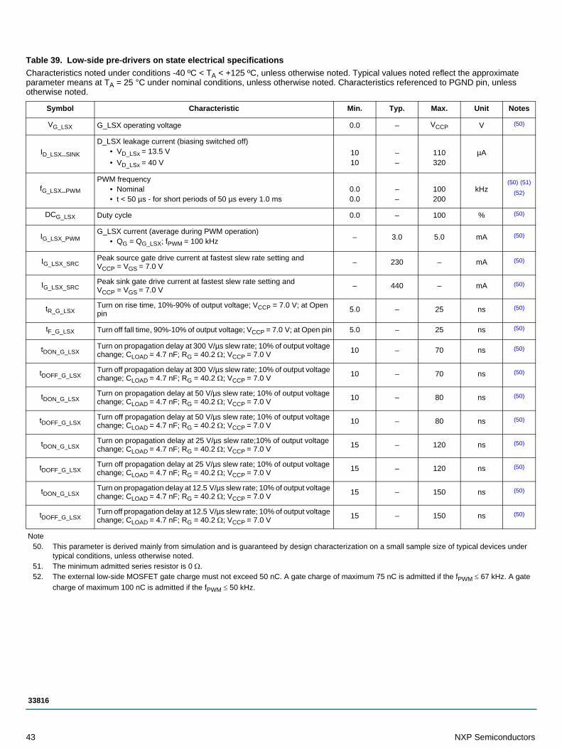
Table 39. Low-side pre-drivers on state electrical specifications
Characteristics noted under conditions -40 ºC < TA < +125 ºC, unless otherwise noted. Typical values noted reflect the approximate parameter means at TA = 25 °C under nominal conditions, unless otherwise noted. Characteristics referenced to PGND pin, unless otherwise noted.
Symbol Characteristic Min. Typ. Max. Unit Notes
VG_LSX G_LSX operating voltage 0.0 – VCCP V (50)
ID_LSX_SINK
D_LSX leakage current (biasing switched off)• VD_LSx = 13.5 V
• VD_LSx = 40 V1010
––
110320
µA
fG_LSX_PWM
PWM frequency• Nominal• t < 50 µs - for short periods of 50 µs every 1.0 ms
0.00.0
––
100200
kHz(50) (51)
(52)
DCG_LSX Duty cycle 0.0 – 100 % (50)
IG_LSX_PWMG_LSX current (average during PWM operation)
• QG = QG_LSX; fPWM = 100 kHz– 3.0 5.0 mA (50)
IG_LSX_SRCPeak source gate drive current at fastest slew rate setting and VCCP = VGS = 7.0 V
– 230 – mA (50)
IG_LSX_SRCPeak sink gate drive current at fastest slew rate setting and VCCP = VGS = 7.0 V
– 440 – mA (50)
tR_G_LSXTurn on rise time, 10%-90% of output voltage; VCCP = 7.0 V; at Open pin
5.0 – 25 ns (50)
tF_G_LSX Turn off fall time, 90%-10% of output voltage; VCCP = 7.0 V; at Open pin 5.0 – 25 ns (50)
tDON_G_LSXTurn on propagation delay at 300 V/µs slew rate; 10% of output voltage change; CLOAD = 4.7 nF; RG = 40.2 ; VCCP = 7.0 V
10 – 70 ns (50)
tDOFF_G_LSXTurn off propagation delay at 300 V/µs slew rate; 10% of output voltage change; CLOAD = 4.7 nF; RG = 40.2 ; VCCP = 7.0 V
10 – 70 ns (50)
tDON_G_LSXTurn on propagation delay at 50 V/µs slew rate; 10% of output voltage change; CLOAD = 4.7 nF; RG = 40.2 ; VCCP = 7.0 V
10 – 80 ns (50)
tDOFF_G_LSXTurn off propagation delay at 50 V/µs slew rate; 10% of output voltage change; CLOAD = 4.7 nF; RG = 40.2 ; VCCP = 7.0 V
10 – 80 ns (50)
tDON_G_LSXTurn on propagation delay at 25 V/µs slew rate;10% of output voltage change; CLOAD = 4.7 nF; RG = 40.2 ; VCCP = 7.0 V
15 – 120 ns (50)
tDOFF_G_LSXTurn off propagation delay at 25 V/µs slew rate; 10% of output voltage change; CLOAD = 4.7 nF; RG = 40.2 ; VCCP = 7.0 V
15 – 120 ns (50)
tDON_G_LSXTurn on propagation delay at 12.5 V/µs slew rate; 10% of output voltage change; CLOAD = 4.7 nF; RG = 40.2 ; VCCP = 7.0 V
15 – 150 ns (50)
tDOFF_G_LSXTurn off propagation delay at 12.5 V/µs slew rate; 10% of output voltage change; CLOAD = 4.7 nF; RG = 40.2 ; VCCP = 7.0 V
15 – 150 ns (50)
Note50. This parameter is derived mainly from simulation and is guaranteed by design characterization on a small sample size of typical devices under
typical conditions, unless otherwise noted.51. The minimum admitted series resistor is 0 .52. The external low-side MOSFET gate charge must not exceed 50 nC. A gate charge of maximum 75 nC is admitted if the fPWM 67 kHz. A gate
charge of maximum 100 nC is admitted if the fPWM 50 kHz.
43 NXP Semiconductors
33816

6.4.2 Low-side pre-driver slew rate controlEach driver strength can be selected individually by the SPI registers within a set of values. There are four selectable driver strengths. The strength for the rising and falling edge can be individually chosen for each driver. A change in the rising edge affects the falling edge such as to keep the same absolute slew rate.
The slew rates are selected by the SPI, writing the Ls_slewrate register (0x18F) while in Normal mode (at reset we are in normal mode), but with the possibility of rapidly changing to the highest slew rate with the microcode instruction stslew.
Table 40. Low-side pre-drivers off state electrical specifications
Characteristics noted under conditions -40 ºC < TA < +125 ºC, unless otherwise noted. Typical values noted reflect the approximate parameter means at TA = 25 °C under nominal conditions, unless otherwise noted. Characteristics referenced to PGND pin, unless otherwise noted.
Symbol Characteristic Min. Typ. Max. Unit Notes
RPD_LSX G_LSX to PGND pull-down resistor 25 50 90 k
Table 41. Low-side pre-drivers slew rate settings
lsx_slewrate_n(1:0) Slew Rate (V/µs)RDSON_PMOS
(switching on) ()RDSON_NMOS
(switching off) ()
00 300 14.6 5.9
01 50 84 35
10 25 170 69
11 12.5 337 138
Table 42. Low-side pre-drivers slew rates characteristics
Characteristics noted under conditions -40 ºC < TA < +125 ºC, unless otherwise noted. Typical values noted reflect the approximate parameter means at TA = 25 °C under nominal conditions, unless otherwise noted.
Symbol Characteristic Min. Typ. Max. Unit Notes
RDS_HSX_P
(00)
G_HSx pMOS RDS_ON (00), 300 V/µs, VCCP = 7.0 V• at external VGS = 2.5 V
• at external VGS = 1.0 to 4.0 V8.87.5
14.6–
25.331.3
W
RDS_HSX_N
(00)
G_HSx nMOS RDS_ON (00), 300 V/µs, VCCP = 7.0 V• at external VGS = 2.5 V
• at external VGS = 1.0 to 4.0 V3.42.5
5.9–
11.116.5
W
RDS_HSX_P
(01)
G_HSx pMOS RDS_ON (01), 50 V/µs, VCCP = 7.0 V• at external VGS = 1.0 to 4.0 V
61 84 115 W
RDS_HSX_N
(01)
G_HSx nMOS RDS_ON (01), 50 V/µs, VCCP = 7.0 V• at external VGS = 1.0 to 4.0 V
23 35 50 W
RDS_HSX_P
(10)
G_HSx pMOS RDS_ON (10), 25 V/µs, VCCP = 7.0 V• at external = 1.0 to 4.0 V
122 170 230 W
RDS_HSX_N
(10)
G_HSx nMOS RDS_ON (10), 25 V/µs, VCCP = 7.0 V• at external VGS = 1.0 to 4.0 V
47 69 100 W
RDS_HSX_P
(11)
G_HSx pMOS RDS_ON (11), 12.5 V/µs, VCCP = 7.0 V• at external VGS = 1.0 to 4.0 V
245 337 460 W
RDS_HSX_N
(11)
G_HSx nMOS RDS_ON (11), 12.5 V/µs, VCCP = 7.0 V• at external VGS = 1.0 to 4.0 V
94 138 199 W
NXP Semiconductors 44
33816

6.4.3 Safe state of low-side pre-driverIn order to guarantee a safe condition, the G_LSX output is immediately forced to a low level, switching off the external MOSFET when a reset is asserted and while the device is not operating. In this phase, the pre-driver is powered by the charge already stored in the VCCP buffer capacitor, and a low level output is guaranteed, as long as a typical voltage greater than 1.1 V is available.When the VCCP supply voltage is lower than 1.1 V, the pre-driver output is pulled to PGND by an internal high resistance RPD_LSX pull-down resistor.
6.5 VDS and VSRC monitor and load biasing
The 33816 provides a VDS monitoring function for diagnostic and protection for each of the five high-side pre-drivers, and for six of the low-side pre-divers. The LS7 pre-driver dedicated to the DC-DC converter does not integrate this diagnosis feature.Moreover, a source voltage monitoring function VSRC populates each of the five high-side pre-drivers. The VDS monitors measure:
• the voltage between the VBOOST or VBATT pin, and the source pin of the external MOSFET connected to the S_HSx device pin, for the HS2 and HS4 high-side pre-drivers
• the voltage between the VBATT pin and the source pin of the external MOSFET connected to the S_HSx device pin, for the HS1, HS3, and HS5 high-side pre-drivers
• the voltage between the drain pin of the external MOSFET connected to the D_LSx device pin and the PGND pin, for the low-side pre-drivers
Figure 17. VDS and VSRC monitors and load biasing
tSLR_HSSlew rate switching time
• 1 ck cycle at 6.0 MHz– – 166 ns (53)
Note53. This parameter is derived mainly from simulation and is guaranteed by design characterization on a small sample size from typical devices under
typical conditions, unless otherwise noted.
Table 42. Low-side pre-drivers slew rates characteristics (continued)
Characteristics noted under conditions -40 ºC < TA < +125 ºC, unless otherwise noted. Typical values noted reflect the approximate parameter means at TA = 25 °C under nominal conditions, unless otherwise noted.
Symbol Characteristic Min. Typ. Max. Unit Notes
45 NXP Semiconductors
33816

Figure 18. VDS monitors and load biasing for HS2 and HS4
The VSRC monitors measure on the high-side pre-drivers, the voltage between the source pin of the external MOSFET connected to the S_HSx device pin and the PGND pin.Their thresholds are individually selectable for each output by setting the suitable values in:
• the Vds_threshold_hs (0x18A) register for the high-side pre-drivers VDS threshold• the Vsrc_threshold_hs (0x18B) register for the high-side pre-drivers VSRC threshold• the Vds_threshlod_ls_1 (0x18C) and Vds_threshlod_ls_1 (0x18D) registers for the low-side pre-drivers VDS threshold
These thresholds are selectable either by the SPI or by microcode (chth instruction).The VDS and VSRC monitor functions are available, since the corresponding pre-drivers are supplied.The high-side VDS and VSRC monitors can work in standalone mode without using the associated high-side pre-driver. In this case, the B_HSX and G_HSX outputs is not connected and the corresponding high-side driver cannot be used. The S_HSX input can be connected to any node, as long as the maximum is within the pin’s maximum rating range.
6.5.1 High-side VDS And VSRC monitoringThe high-side VDS and VSRC monitors are functionally independent from the bootstrap voltage of the high-side pre-driver.The two high-side VDS monitors of pre-driver 2 and 4 are composed of three comparators with programmable thresholds, the first one senses the voltage between VBOOST and the S_HSX source pin (VDS of the high-side MOSFET used as boost MOSFET). The second one senses the voltage between VBATT and the S_HSX source pin (VDS of the high-side MOSFET, used as a battery MOSFET and voltage information for voltage based diagnosis, when the MOSFET is in boost configuration) The third one senses the voltage between the S_HSX source pin and PGND (voltage across the freewheeling element, either a diode or a MOSFET).The instruction slfbk allows to select which of the two feedbacks hsx_vds_vboost_fbk or hsx_vds_vbatt_fbk, enables the microcores.Two voltage references per high-side pre-driver provide a voltage threshold to the VDS comparators. Their values are selectable among eight values, according to the hsx_vds_threshold(2:0) and the hsx_src_threshold(2:0) signal, provided by the digital cores.The current values of the hsx_vds_threshold(2:0) and the hsx_src_threshold(2:0) are programmed through the SPI by accessing the Vds_regfile registers (0x18A and 0x18B).
�����
����
���
�� �
����
����
����
����
����
�����������
�������������������� ! ����"�����������
��������#����$#%
�����&�������������� !����"��
���������
�����&�$#%
�
�
�
�
��'
�("���(��
����)��(�
������*�
�+�
���*
���
,��-�*
(���(*
"����*
��+
�,�./
�����
��������#�����$#%�
�
NXP Semiconductors 46
33816

If a fast dv/dt is applied (the SRS_HSX maximum value is exceeded) at the S_HSX pin (for instance, during boost MOSFET commutations), the comparator output may have an incorrect value while the disturbance is applied. The function recovers after the disturbance removal to the nominal behavior in less than a typical 300 ns.During freewheeling operation, the S_HSX source pin, can go down to a typical -3.0 V, and can withstand transients of -6.0 V/-8.0 V for a duration shorter than 400 ns at a very high MOSFET switch.
Table 43. VDS and VSRC monitoring typical threshold selection for high-side pre-drivers
hsx_vds/src_ threshold(2:0) VDS (V) VSRC (V)
000 0.00 0.0
001 0.5 0.5
010 1 1
011 1.5 1.5
100 2.0 2.0
101 2.45 2.5
110 2.95 3.0
111 3.45 3.5
Table 44. High-side VDS and VSRC monitoring electrical specifications
Characteristics noted under conditions -40 ºC < TA < +125 ºC, unless otherwise noted. Typical values noted reflect the approximate parameter means at TA = 25 °C under nominal conditions, unless otherwise noted. Characteristics referenced to PGND pin, unless otherwise noted.
Symbol Characteristic Min. Typ. Max. Unit Notes
VS_HS_VDS
High-side VDS/SRC monitoring functional range S_HSx• Transients t < 400 ns• Transients t < 800 ns
-3.0-8.0-6.0
–––
72––
V (54)
VVBATT_VDSHigh-side VDS/SRC monitoring functional range VBATT
• VDS_HS_TH 3.5 V is at 3.0 V min.5.55.0
––
725.5
V
VVBOOST_VDSHigh-side VDS/SRC monitoring functional range VBOOST
• VDS_HS_TH 3.5 V is at 3.0 V min.5.55.0
––
725.5
V
VDS_HS_TH
High-side VDS threshold (000)• VVBATT_VDS = 5.0 V to 72 V
• VVBOOST_VDS = 5.0 V to 72 V-0.1 0.0 0.1 V
VDS_HS_TH
High-side VDS threshold (001)• VVBATT_VDS = 5.0 V to 72 V
• VVBOOST_VDS = 5.0 V to 72 V0.4 0.5 0.6 V
VDS_HS_TH
High-side VDS threshold (010)• VVBATT_VDS = 5.0 V to 72 V
• VVBOOST_VDS = 5.0 V to 72 V0.9 1.0 1.1 V
VDS_HS_TH
High-side VDS threshold (011)• VVBATT_VDS = 5.0 V to 72 V
• VVBOOST_VDS = 5.0 V to 72 V1.35 1.5 1.65 V
VDS_HS_TH
High-side VDS threshold (100)• VVBATT_VDS = 5.0 V to 72 V
• VVBOOST_VDS = 5.0 V to 72 V1.8 2.0 2.2 V
VDS_HS_TH
High-side VDS threshold (101)• VVBATT_VDS = 5.0 V to 72 V
• VVBOOST_VDS = 5.0 V to 72 V2.29 2.45 2.61 V
47 NXP Semiconductors
33816

VDS_HS_TH
High-side VDS threshold (110)• VVBATT_VDS = 5.0 V to 72 V
• VVBOOST_VDS = 5.0 V to 72 V2.76 2.95 3.14 V
VDS_HS_TH
High-side VDS threshold (111)• VVBATT_VDS = 5.5 V to 72 V
• VVBOOST_VDS = 5.5 V to 72 V
• VVBATT_VDS = 5.0 V to 5.5 V
• VVBOOST_VDS = 5.0 V to 5.5 V
3.233.233.03.0
3.53.5
3.453.45
3.673.673.673.67
V
tTH_HSVDSHigh-side VDS/SRC threshold settling time
• From HS_VDS/SRC_threshold(2:0) change to threshold stable– 0.4 1.0 µs (54)
tD_HSVDS
High-side VDS/SRC comparator switching time, Propagation delay + rise/fall time
• At 100 mV overdrive• At 200 mV overdrive• At 300 mV overdrive
–––
1.00.80.6
1.51.11.0
µs (54)(55)
tR_HSVDSHigh-side VDS/SRC comparator recovery time after dVD/dt
• Recovery time after dVD/dt is removed– – 300 ns (54)
SRHSVDS
High-side VDS/SRC comp. input voltage slew rate with good output at VDS_HS=0.75 V with VS_HSx from 13.5 V to 72 V and from 72 V to 13.5 V
– – 100 V/µs (54)
VSRC_HS_TH High-side VSRC threshold (000) -0.1 0.0 0.1 V
VSRC_HS_TH High-side VSRC threshold (001) 0.4 0.5 0.6 V
VSRC_HS_TH High-side VSRC threshold (010) 0.9 1.0 1.1 V
VSRC_HS_TH High-side VSRC threshold (011) 1.35 1.5 1.65 V
VSRC_HS_TH High-side VSRC threshold (100) 1.8 2.0 2.2 V
VSRC_HS_TH High-side VSRC threshold (101) 2.38 2.55 2.72 V
VSRC_HS_TH High-side VSRC threshold (110) 2.85 3.0 3.15 V
VSRC_HS_TH High-side VSRC threshold (111) 3.33 3.5 3.68 V
VSRC_HS_Th High‐side VSRC threshold (000) including crosstalk -0.2 0.0 0.2 V (54)(56)
VSRC_HS_Th High‐side VSRC threshold (001) including crosstalk 0.3 0.5 0.7 V (54)(56)
VSRC_HS_Th High‐side VSRC threshold (010) including crosstalk 0.8 1.0 1.2 V (54)(56)
VSRC_HS_Th High‐side VSRC threshold (011) including crosstalk 1.25 1.5 1.75 V (54)(56)
VSRC_HS_Th High‐side VSRC threshold (100) including crosstalk 1.7 2.0 2.3 V (54)(56)
VSRC_HS_Th High‐side VSRC threshold (101) including crosstalk 2.28 2.55 2.82 V (54)(56)
VSRC_HS_Th High‐side VSRC threshold (110) including crosstalk 2.75 3.0 3.25 V (54)(56)
Table 44. High-side VDS and VSRC monitoring electrical specifications (continued)
Characteristics noted under conditions -40 ºC < TA < +125 ºC, unless otherwise noted. Typical values noted reflect the approximate parameter means at TA = 25 °C under nominal conditions, unless otherwise noted. Characteristics referenced to PGND pin, unless otherwise noted.
Symbol Characteristic Min. Typ. Max. Unit Notes
NXP Semiconductors 48
33816

6.5.2 Low-side VDS monitoringA comparator with a programmable threshold is provided for VDS monitoring of the external low-side MOSFET, sensing the voltage between the D_LSx drain pin and PGND (VDS of the low-side MOSFET). If a sense resistor is connected between the low-side MOSFET and ground, the voltage drop on the resistor is included in the measurement.One voltage reference per low-side pre-driver provides a voltage threshold to the VDS comparator. Its value is selectable among eight values, according to the lsx_vds_threshold(2:0) signal, provided by the digital cores. The current values of lsx_vds_threshold(2:0) are programmed through the SPI by accessing the Vds_regfile registers (0x18C and 0x18D).
If a fast dv/dt is applied at the D_LSX pin (for instance, after a fast decay), the comparator output may have an incorrect value. When a disturbance is applied, the function recovers from the disturbance removal to a nominal behavior in less than a typical 300 ns.The operating voltage range of low-side MOSFET D_LSX drain pin is up to 75 V. During freewheeling operation on one load, the D_LSX source pin of a different load connected to the same bank, can go down to a typical -3.0 V.The low-side VDS monitors can even be used standalone, without using the associated low-side pre-driver. In this case, the G_LSX output is not connected. The D_LSX input can be connected to any node within the pin maximum ratings voltage range.
VSRC_HS_Th High‐side VSRC threshold (111) including crosstalk 3.23 3.5 3.78 V (54)(56)
Note54. This parameter is derived mainly from simulation and is guaranteed by design characterization on a small sample size of typical devices under
typical conditions, unless otherwise noted.55. The high value is a worst case consideration on an overdrive of 100 mV.56. To limit the amplitude of the crosstalk to the specified value, the sequence of monitor threshold switching must not exceed a certain number of
switches in any given time window. Any sequence of n commands which increase a threshold of a low-side VDS or high-side VSRC monitor must be spread over a time window tN_I which meets the condition: tN_I (N - 7) * 1.67 µs. Any sequence of m commands which decrease a threshold
must be spread over a time window tM_D which meets the condition: tM_D (M - 7) * 1.67 µs.
Table 45. VDS monitoring typical threshold selection for low-side pre-drivers
lsx_vds threshold(2:0) VDS (V)
000 0.00
001 0.5
010 1.0
011 1.5
100 2.0
101 2.5
110 3.0
111 3.5
Table 46. Low-side VDS monitoring electrical specifications
Characteristics noted under conditions -40 ºC < TA < +125 ºC, unless otherwise noted. Typical values noted reflect the approximate parameter means at TA = 25 °C under nominal conditions, unless otherwise noted. Characteristics referenced to PGND pin, unless otherwise noted.
Symbol Characteristic Min. Typ. Max. Unit Notes
VD_LSX_VDSLow-side VDS monitoring functional range D_LSx
• Transients t < 400 ns-3.0-8.0
––
75–
V (57)
VDS_LS_TH Low-side VDS threshold (000) -0.1 0.0 0.1 V
VDS_LS_TH Low-side VDS threshold (001) 0.4 0.5 0.6 V
VDS_LS_TH Low-side VDS threshold (010) 0.9 1.0 1.1 V
Table 44. High-side VDS and VSRC monitoring electrical specifications (continued)
Characteristics noted under conditions -40 ºC < TA < +125 ºC, unless otherwise noted. Typical values noted reflect the approximate parameter means at TA = 25 °C under nominal conditions, unless otherwise noted. Characteristics referenced to PGND pin, unless otherwise noted.
Symbol Characteristic Min. Typ. Max. Unit Notes
49 NXP Semiconductors
33816

6.5.3 Load biasing structuresTo enable electrical diagnosis while the external load is not actuating the power stage, a voltage biasing VBIAS should be applied to the load, during the idle phases.This VBIAS voltage is generated by:
• the activation of each pull-up voltage source SRCPUX connected to each of the S_HSx pins. Each pull-up voltage source is supplied from VCC5.
• the activation of each pull-down current sources SRCPDX connected to each of the D_LSx pins. Each pull-down voltage source referenced to ground.
When the battery voltage VBATT is in the nominal range or greater, the external load is biased at a minimum voltage of typically 3.8 V. In a low battery voltage condition (VBATT < 8.0 V), the load is biased at half the VBATT voltage, to guarantee symmetrical voltage margins to high-side and low-side VDS comparators.
VDS_LS_TH Low-side VDS threshold (011) 1.35 1.5 1.65 V
VDS_LS_TH Low-side VDS threshold (100) 1.8 2.0 2.2 V
VDS_LS_TH Low-side VDS threshold (101) 2.38 2.5 2.63 V
VDS_LS_TH Low-side VDS threshold (110) 2.85 3.0 3.15 V
VDS_LS_TH Low-side VDS threshold (111) 3.33 3.5 3.68 V
VDS_LS_Th Low‐side VDS threshold (000) incl. crosstalk -0.2 0.0 0.2 V (57)(58)
VDS_LS_Th Low‐side VDS threshold (001) incl. crosstalk 0.3 0.5 0.7 V (57)(58)
VDS_LS_Th Low‐side VDS threshold (010) incl. crosstalk 0.8 1.0 1.2 V (57)(58)
VDS_LS_Th Low‐side VDS threshold (011) incl. crosstalk 1.25 1.5 1.75 V (57)(58)
VDS_LS_Th Low‐side VDS threshold (100) incl. crosstalk 1.7 2.0 2.3 V (57)(58)
VDS_LS_Th Low‐side VDS threshold (101) incl. crosstalk 2.28 2.5 2.73 V (57)(58)
VDS_LS_Th Low‐side VDS threshold (110) incl. crosstalk 2.75 3.0 3.25 V (57)(58)
VDS_LS_Th Low‐side VDS threshold (111) incl. crosstalk 3.23 3.5 3.78 V (57)(58)
tTH_LSVDS Low-side VDS threshold settling time – 0.4 1.0 µs (57)
tD_LSVDSLow-side VDS comparator switching time
• From LS_VDS_TH(1:0) change to VDS_LSTH stable– 0.3 1.0 µs (57)
tR_LSVDSLow-side VDS comparator recovery time after dVD/dt
• Recovery time after dVD/dt is removed– – 300 ns (57)
Note57. This parameter is derived mainly from simulation and is guaranteed by design characterization on a small sample size of typical devices under
typical conditions, unless otherwise noted.58. To limit the amplitude of the crosstalk to the specified value, the sequence of monitor threshold switching must not exceed a certain number of
switches in any given time window. Any sequence of n commands which increase a threshold of a low-side VDS or high-side VSRC monitor must be spread over a time window tN_I which meets the condition: tN_I >= (n - 7) * 1.67 µs. Any sequence of m commands which decrease a threshold
must be spread over a time window tM_D which meets the condition: tM_D >= (M - 7) * 1.67 µs.
Table 46. Low-side VDS monitoring electrical specifications (continued)
Characteristics noted under conditions -40 ºC < TA < +125 ºC, unless otherwise noted. Typical values noted reflect the approximate parameter means at TA = 25 °C under nominal conditions, unless otherwise noted. Characteristics referenced to PGND pin, unless otherwise noted.
Symbol Characteristic Min. Typ. Max. Unit Notes
NXP Semiconductors 50
33816

Figure 19. Biasing Voltage vs. VBATT
If there is no load connected to the S_HSX pin, the voltage at this node can raise higher than VCC5, due to leakage currents from VBOOST and VBATT. All pull-up and pull-down structures could be switched on or off independently, under the control of the digital microcores, using the control signals hsx_bias, hsx_bias_strong, and lsx_bias. All the biasings can be enabled by the microcores using the bias instruction.To prevent overloading on VCC5, switching on all the high-side pull-up structures simultaneously is not possible.
The pull-up voltage sources are switched off automatically, as soon as a VCC5 voltage is exceeded at the S_HSX pin. The voltage divider to generate the VBATT/2 reference is disconnected from the VBATT pin as soon as RSTB is activated.The load biasing sources can be used standalone, without using the associated low-side or high pre-driver. The D_LSX and S_HSX outputs can be connected to any node within the pin’s maximum rating voltage range.The pull-down current sources at D_LSx can also be used to slowly charge the bootstrap capacitors, after a key ON via the bootstrap path, without switching on the low-side MOSFETs. In this case, the corresponding pull-up voltage sources must be disabled.
Table 47. Load biasing HS2 and HS4 control table
hsx_bias hsx_bias_strongCurrent limitation (mA)
Min value Max value
0 0 Biasing off Biasing off
1 0 2.8 5.2
0 1 4.2 7.8
1 1 7.0 13.0
Table 48. Load biasing electrical specifications
Characteristics noted under conditions -40 ºC < TA < +125 ºC, unless otherwise noted. Typical values noted reflect the approximate parameter means at TA = 25 °C under nominal conditions, unless otherwise noted. Characteristics referenced to PGND pin, unless otherwise noted.
Symbol Characteristic Min. Typ. Max. Unit Notes
IBIAS_HS Current source S_HSx (x = 1... 5) source current limitation 2.8 4.0 5.2 mA
IBIAS_HS_STRONG Current source S_HSx (x = 2, 4) source current limitation 4.2 6.0 7.8 mA
IBIAS_HS_MAXTotal maximum current source S_HSx source current
• Maximum current from VCC526 – – mA
IBIAS_LS Current source D_LSx (x = 1...6) sink saturation current 0.98 1.09 1.2 mA
VBIAS_HS
S_HSx bias voltage regulation• VBATT > 8.0 V, VCC5 > 4.75 V• VBATT < 8.0 V, VCC5 > 4.75 V
3.8(VBATT/2) -
200 mV
–VBATT/2
VCC5
(VBATT/2) + 200 mV
V (60)(60)
VS_HS_BIAS
S_HSx voltage range when load biasing is switched on (S_HSx current source is switched off automatically when S_HSx is above 5.0 V)
• Transients t < 400 ns• Transients t < 800 ns
-3.0-8.0-6.0
–––
72––
V (60)
VD_LSX_BIASD_LSx voltage range when load biasing is switched on
• Transients t < 400 ns-3.0-8.0
––
75–
V (60)
51 NXP Semiconductors
33816

6.6 Current measurement
Four current measurement blocks are implemented into the 33816:• Three general purpose blocks• One extended mode block for DC-DC Converters
6.6.1 General purpose current measurement blockThe actuator current flowing in an external sense resistor is measured to implement a closed loop current control. The current measurement block is comprised of a differential amplifier, sensing the voltage across the sense resistor, a voltage comparator, and an 8-bit current DAC.
Figure 20. General purpose current measurement block diagram
VBIAS_HS
Voltage dropout across HS1/3/5 current source• VCC5 = 4.75 V, IBIAS_HS1/3/5 = 2.8 mA, IBIAS_HS_Max = 18.4 mA
– – 0.95 V
VBIAS_HS
Voltage dropout across HS2/4 current source• VCC5 = 4.75 V, IBIAS_HS2/4 = 7.0 mA, IBias_HS_Max = 18.4 mA
– – 0.95 V
VBIAS_LS
Voltage dropout across LS current source• IBIAS_LS = saturation current• IBIAS_LS = 500 µA• IBIAS_LS = 300 µA
–––
–––
2.5700400
VmVmV
RBIAS_LSEquivalent resistance of LS current source
• VD_LSx < 1.0 V0.5 – 1.5 k
CS_HSXS_HSx capacitive load to GND connected via, L = 2.0 nH… 200 nH and R = 2.0 m… 200 m 0.01 – 25 nF (60)
Note59. The VBIAS_HS value is specified with a load series resistor load and the corresponding low-side and high-side load biasing turned on.
60. This parameter is derived mainly from simulation and is guaranteed by design characterization on a small sample size of typical devices under typical conditions, unless otherwise noted.
Table 48. Load biasing electrical specifications (continued)
Characteristics noted under conditions -40 ºC < TA < +125 ºC, unless otherwise noted. Typical values noted reflect the approximate parameter means at TA = 25 °C under nominal conditions, unless otherwise noted. Characteristics referenced to PGND pin, unless otherwise noted.
Symbol Characteristic Min. Typ. Max. Unit Notes
NXP Semiconductors 52
33816

The differential amplifier gain is selectable among four different values by means of the opamapx_gain(1:0) signal, to get the suitable signal amplification. The gain can be changed at runtime by the microcore.The differential amplifier also adds a constant offset to its output. Therefore, the output of the amplifier is always positive.The desired actuator current level can be selected and changed at runtime by the microcore, setting the proper threshold value dacx_Value (7:0) in the DAC. Each current measurement channel can be used in ADC mode. A track and hold circuit is implemented to keep the voltage at the comparator input stable during the ADC conversion.The differential amplifier output can be routed to an external pin (OA_1 and OA_2). In this configuration, the device output is usually connected to an ADC input of the MCU for safety and test purposes. The output multiplexer block contains an output amplifier with selectable gain by means of the oa_gainy(1:0) signal, providing full swing output on OA_y for A/D conversion, if used with 3.3 V or 5.0 V applications. All the analog blocks for current measurement are supplied by the VCC5 power supply and referenced to the analog ground, AGND.
6.6.2 Current sense amplifierThe current sense amplifier provides a voltage as detailed by the following:
• VDA_SENSE = (VVSENSEPx - VVSENSENx) * GDA_DIFF + VDA_BIAS
VDA_BIAS is the fixed voltage biasing applied to the differential amplifier output.The GDA_DIFF gain value is configurable at runtime (opampx_gain(1:0)).The allowed differential mode input voltages depend on the chosen gain value.
• VDA_DIFF_IN = (VVSENSEPx - VVSENSENx)
The amplifier can achieve even lower voltages than VDA_BIAS, when the differential input voltage is below zero, to make it able to measure small negative currents. The amplifier is fully operational down to an output voltage of typically 100 mV. The amplifier is not designed to be used with series resistors between shunt and VSENSEPx/VSENSENx inputs. Detection delay including comparators, is typically 50 to 500 ns, depending on gain setting, set point value, and input voltage slew rate.
Table 49. Overall current sense performance for positive current measurement
Characteristics noted under conditions -40 ºC < TA < +125 ºC, unless otherwise noted. Typical values noted reflect the approximate parameter means at TA = 25 °C under nominal conditions, unless otherwise noted.
Symbol CharacteristicStatistically Evaluated
Unit Notes
eCS
Overall current sense error including gain errors and offsets at DAC range of 75%-100%, after analog offset compensation.
• at GDA_diff(00) = 5.79• at GDA_diff(01) = 8.68• at GDA_diff(10) = 12.53• at GDA_diff(11) = 19.25
at DAC range of 25%-75%, after analog offset compensation.• at GDA_diff(00) = 5.79• at GDA_diff(01) = 8.68• at GDA_diff(10) = 12.53• at GDA_diff(11) = 19.25
±3.5±3.5±3.6±3.7
±5.3±5.4±5.4±5.4
% (61)
Note61. All input tolerances from the device specification are assumed at 6.0 .
Table 50. Current sense amplifier overall gain selection table
Opampx_ gain(1:0) Gain valueNormal differential mode typical
input voltage range (mV)Full scale current range with
10 mshunt (A)Typical DAC resolution with
10 m shunt (mA)
00 5.79 -25.9 to 387 -2.59 to 38.7 169
01 8.68 -17.3 to 258 -1.73 to 25.8 113
10 12.53 -12.0 to 179 -1.20 to 17.9 78
11 19.25 -7.8 to 116 -0.78 to 11.6 51
53 NXP Semiconductors
33816

Table 51. Differential amplifiers 1, 2, 3, 4H, and 4L electrical specifications
Characteristics noted under conditions -40 ºC < TA < +125 ºC, unless otherwise noted. Typical values noted reflect the approximate parameter means at TA = 25 °C under nominal conditions, unless otherwise noted. Characteristics referenced to PGND pin, unless otherwise noted.
Symbol Characteristic Min. Typ. Max. Unit Notes
VVSENSENX_DA
Differential amplifier x functional range VSENSENX (x = 1, 2, 3, 4H, 4L)At VSENSENX/P voltage below -1.0 V, the differential amplifier for positive current measurement can produce an output voltage > 0.0 V, even if the differential voltage at the input is < 0.0 V.
-1.0 – 1.0 V (62)
VVSENSEPX_DA
Differential amplifier x functional range VSENSEPX (x = 1, 2, 3, 4H, 4L)At VSENSEN/P voltage of below -1.0 V the differential amplifier for positive current measurement can produce an output voltage > 0.0 V even if the differential voltage at the input is < 0.0 V.
-1.0 – 1.5 V (62)
VDA_DIFF_INDifferential input voltage range (00)
• GDA_DIFF(00) = 5.79-25.9 – 387 mV (62)
VDA_DIFF_INDifferential input voltage range (01)
• GDA_DIFF(01) = 8.68-17.3 – 258 mV (62)
VDA_DIFF_INDifferential input voltage range (10)
• GDA_DIFF(10) = 12.53-12 – 179 mV (62)
VDA_DIFF_INDifferential input voltage range (11)
• GDA_DIFF(11) = 19.25-7.8 – 116 mV (62)
GDA_DIFF(00) Differential voltage gain (00) 5.71 5.79 5.87
GDA_DIFF(01) Differential voltage gain (01) 8.55 8.68 8.81
GDA_DIFF(10) Differential voltage gain (10) 12.32 12.53 12.74
GDA_DIFF(11) Differential voltage gain (11) 18.92 19.25 19.58
tDA_GAIN_SW Gain switching settling time – – 2.0 µs (62)
SRDA_DIFF_IN Differential input voltage maximum slew rate 140 – – mV/µs (62)(63)
RVSENSENX_INInput impedance VSENSENX (x = 1, 2, 3)
• 1.0 V common mode voltage18 – 36 k
RVSENSEPX_INInput impedance VSENSEPX (x = 1, 2, 3)
• 1.0 V common mode voltage18 – 36 k
VDA_BIAS Output bias voltage 240 250 265 mV
VDA_OUT_OFF
Maximum output offset voltage error at maximum gain; Including amplifier input offset and bias voltage offset. Calculated using the highest gain of 19.25
-140 – 220 mV .
VDA_OUT Differential amplifier x output voltage range 0.1 – 2.7 V
SRDA Differential amplifier x output slew rate 2.8 – – V/µs (62)
Note62. This parameter is derived mainly from simulation and is guarantee by design characterization on a small sample size of typical devices under
typical conditions, unless otherwise noted.63. Considering an external output capacitor CVSENSE typically value of 330 pF. This external capacitor is recommended for improve EMI
performances.
NXP Semiconductors 54
33816

6.6.3 Current sense DACIn order to select the proper threshold for current control, an 8-bit current DAC is implemented to provide a threshold to the voltage comparator (dacy_Value (7:0)). The current threshold can be calculated using the following formula.
• I = (DAC_VALUE * VDAC LSB- VDA_BIAS)/(GDA_DIFF * RSENSEx)
The DAC_VALUE is selected and changed at runtime by the digital microcore by means of the signal dacx_value (7:0). A DAC_VALUE below the hexadecimal value 0x0A, must be avoided, as the current sense differential amplifier does not operate with full performance at output voltages below 100 mV.VDAC LSB is the DAC resolution.VDA_BIAS is the fixed voltage biasing applied to the differential amplifier output.The Gain Value GDA_DIFF is configurable at runtime (opampx_gain(1:0)).RSENSEx is the external sense resistor of the current measurement channel x.
Table 52. Current sense DAC values examples
DAC value (hex) DAC value (dec)DACoutput
voltage (mV)
Current threshold through 10 m shunt (A)
Differential voltage gain code = 00
Differential voltage gain code = 01
Differential voltage gain code = 10
Differential voltage gain code = 11
0A 10 98 -2.63 -1.76 -1.22 -0.79
… … … … … … …
0F 15 146 -1.79 -1.19 -0.83 -0.54
… … … … … … …
19 25 244 -0.1 -0.07 -0.05 -0.03
1A 26 254 0.07 0.05 0.03 0.02
1B 27 264 0.24 0.16 0.11 0.07
1C 28 273 0.4 0.27 0.19 0.12
1D 29 283 0.57 0.38 0.26 0.17
1E 30 293 0.74 0.5 0.34 0.22
1F 31 303 0.91 0.61 0.42 0.27
20 32 313 1.08 0.72 0.5 0.32
21 33 322 1.25 0.83 0.58 0.38
22 34 332 1.42 0.95 0.65 0.43
23 35 342 1.59 1.06 0.73 0.48
… … … … … … …
32 50 488 4.12 2.75 1.9 1.24
… … … … … … …
64 100 977 12.55 8.37 5.8 3.77
… … … … … … …
96 150 1465 20.98 14 9.7 6.31
… … … … … … …
FF 255 2490 38.69 25.81 17.88 11.64
55 NXP Semiconductors
33816

6.6.4 Current sense comparatorThe voltage comparator toggles when the differential amplifier output exceeds the threshold provided by the DAC. The comparator output is high if the differential amplifier output is greater than the DAC output. No hysteresis is implemented. The curx_fbk comparator output is directly acquired by the digital microcore.
The detection delay from current threshold, reached to the curx_fbk comparator output toggling, is provided in Table 55.
Table 53. DAC 1, 2, 2, 4L and 4H electrical specifications
Characteristics noted under conditions -40 ºC < TA < +125 ºC, unless otherwise noted. Typical values noted reflect the approximate parameter means at TA = 25 °C under nominal conditions, unless otherwise noted. Characteristics referenced to PGND pin, unless otherwise noted.
Symbol Characteristic Min. Typ. Max. Unit Notes
VDAC_LSB DAC LSB – 9.77 – mV
VDAC_OUT_MINDAC minimum output voltage
• DAC code = 0x00 – 0.0 –V
VDAC_OUT_MAXDAC maximum output voltage
• DAC code = 0xFF – 2.49 –V
EDAC_GAIN DAC maximum gain error; error of bandgap reference voltage -1.0 – 1.0 %
EDAC_DNL DAC differential linearity error -0.5 – 0.5 LSB
EDAC_INL DAC integral linearity error -1.0 – 1.0 LSB
VDAC_OUT_OFF DAC maximum output offset 0.0 – 10 mV
tDAC DAC settling time – – 0.9 µs (64)
Note64. This parameter is derived mainly from simulation and is guaranteed by design characterization on a small sample size of typical devices under
typical conditions, unless otherwise noted.
Table 54. Comparator electrical specifications
Characteristics noted under conditions -40 ºC < TA < +125 ºC, unless otherwise noted. Typical values noted reflect the approximate parameter means at TA = 25 °C under nominal conditions, unless otherwise noted. Characteristics referenced to PGND pin, unless otherwise noted.
Symbol Characteristic Min. Typ. Max. Unit Notes
VCOMP_IN Comparator input voltage 0.0 – 2.7 V (65)
VCOMP_IN_OFF Comparator input offset voltage -25 – 10 mV
Note65. This parameter is derived mainly from simulation and is guaranteed by design characterization on a small sample size of typical devices under
typical conditions, unless otherwise noted.
NXP Semiconductors 56
33816

Table 55. Current measurement channel 1, 2, 3, and 4H and 4L detection delays specifications
Characteristics noted under conditions -40 ºC < TA < +125 ºC, unless otherwise noted. Typical values noted reflect the approximate parameter means at TA = 25 °C under nominal conditions, unless otherwise noted. Characteristics referenced to PGND pin, unless otherwise noted.
Symbol Characteristic Min. Typ. Max. Unit Notes
tD_CSDetection delay coming from differential amplifier and comparator at GDA_DIFF(00) = 5.79
20 – 500 ns
tD_CS_150_SLOW
Detection delay coming from differential amplifier and comparator for set point value 150 mV and input voltage slew rate of 2.0 mV/µs
• GDA_DIFF(00) = 5.79
• GDA_DIFF(01) = 8.68
• GDA_DIFF(10) = 12.53
• GDA_DIFF(11) = 19.25
80100130140
––––
260270320400
ns (66)
tD_CS_SLOW
Detection delay coming from differential amplifier and comparator for set point value 400 mV to 2.35 V and input voltage slew rate of 2.0 mV/µs
• GDA_DIFF(00) = 5.79
• GDA_DIFF(01) = 8.68
• GDA_DIFF(10) = 12.53
• GDA_DIFF(11) = 19.25
4590
110140
––––
260280300350
ns (66)
tD_CS_150_MID
Detection delay coming from differential amplifier and comparator for set point value 150 mV and input voltage slew rate of 20 mV/µs
• GDA_DIFF(00) = 5.79
• GDA_DIFF(01) = 8.68
• GDA_DIFF(10) = 12.53
• GDA_DIFF(11) = 19.25
8085
100120
––––
200220260300
ns (66)
tD_CS_MID
Detection delay coming from differential amplifier and comparator for set point value 400 mV to 2.35 V and input voltage slew rate of 20 mV/µs
• GDA_DIFF(00) = 5.79
• GDA_DIFF(01) = 8.68
• GDA_DIFF(10) = 12.53
• GDA_DIFF(11) = 19.25
555080
100
––––
170180200240
ns (66)
tD_CS_150_FAST
Detection delay coming from differential amplifier and comparator for set point value 150 mV and input voltage slew rate of 140 mV/µs
• GDA_DIFF(00) = 5.79
• GDA_DIFF(01) = 8.68
• GDA_DIFF(10) = 12.53
• GDA_DIFF(11) = 19.25
607080
100
––––
160180220280
ns (66)
tD_CS_FAST
Detection delay coming from differential amplifier and comparator for set point value 400 mV to 2.35 V and input voltage slew rate of 140 mV/µs
• GDA_DIFF(00) = 5.79
• GDA_DIFF(01) = 8.68
• GDA_DIFF(10) = 12.53
• GDA_DIFF(11) = 19.25
505580
100
––––
115130160200
ns (66)
tD_CS_SLOW
Detection delay transition 0 to 1 coming from differential amplifier and comparator for input voltage slew rate of 20 mV/µs
• GDA_DIFF(00) = 5.79 and set point value of 300 mV to 2.35 V
• GDA_DIFF(01) = 8.68 and set point value of 300 mV to 2.35 V
• GDA_DIFF(10) = 12.53 and set point value of 300 mV to 2.35 V
• GDA_DIFF(11) = 19.25 and set point value of 300 mV to 2.35 V
705580
110
––––
140150190250
ns (66)
57 NXP Semiconductors
33816

6.6.5 Current measurement offset compensationAn analog offset compensation balances the input offset of the current measurement amplifiers 1 to 4. The offset compensation enablement is managed by the digital microcores. The offset compensation must be calibrated while there is no current flowing through the sense resistor of the related measurement channel.To perform the offset compensation, the DAC output voltage must be set to the bias voltage corresponding to the digital value 0x1A. This DAC is automatically set-up when the offset compensation is started by the digital core, using the stoc instruction. At the end of the offset compensation sequence, the curx_fbk comparator output signal is always low.Each new offset compensation starts, based on the result of the previous offset compensation run, for this current measurement channel. If the offset compensation is stopped from the digital microcore while the analog offset compensation is not finished, the procedure is aborted, maintaining the last compensation value reached when the procedure was interrupted. A residual output offset, after offset compensation completion VOFFDAC_LSB, can remain for the path via the comparator to the feedback signal, and VCS_OAX_OFF when using the path to the OA_x amplifier input.The offset compensation should be done for the maximum differential amplifier gain value used in the application. The offset compensation must be performed when a large device temperature change is expected, due to a temperature drift of the differential amplifier input offset.
tD_CS_SLOW
Detection delay transition 1 to 0 coming from differential amplifier and comparator for input voltage slew rate of 20 mV/µs
• GDA_DIFF(00) = 5.79 and set point value of 300 mV to 2.35 V
• GDA_DIFF(01) = 8.68 and set point value of 300 mV to 2.35 V
• GDA_DIFF(10) = 12.53 and set point value of 300 mV to 2.35 V
• GDA_DIFF(11) = 19.25 and set point value of 300 mV to 2.35 V
608590
120
––––
180200220270
ns (66)
tD_CS_FAST
Detection delay transition 0 to 1 coming from differential amplifier and comparator for input voltage slew rate of 140 mV/µs
• GDA_DIFF(00) = 5.79 and set point value of 300 mV to 2.35 V
• GDA_DIFF(01) = 8.68 and set point value of 300 mV to 2.35 V
• GDA_DIFF(10) = 12.53 and set point value of 300 mV to 2.35 V
• GDA_DIFF(11) = 19.25 and set point value of 300 mV to 2.35 V
50557590
––––
120140160190
ns (66)
tD_CS_FAST
Detection delay transition 1 to 0 coming from differential amplifier and comparator for input voltage slew rate of 140 mV/µs
• GDA_DIFF(00) = 5.79 and set point value of 300 mV to 2.35 V
• GDA_DIFF(01) = 8.68 and set point value of 300 mV to 2.35 V
• GDA_DIFF(10) = 12.53 and set point value of 300 mV to 2.35 V
• GDA_DIFF(11) = 19.25 and set point value of 300 mV to 2.35 V
55657595
––––
130150170210
ns (66)
Note66. This parameter is derived mainly from simulation and is guaranteed by design characterization on a small sample size of typical devices under
typical conditions, unless otherwise noted.
Table 56. Differential amplifier 1, 2, 3, 4L, and 4H analog offset compensation electrical specifications
Characteristics noted under conditions -40 ºC < TA < +125 ºC, unless otherwise noted. Typical values noted reflect the approximate parameter means at TA = 25 °C under nominal conditions, unless otherwise noted. Characteristics referenced to PGND pin, unless otherwise noted.
Symbol Characteristic Min. Typ. Max. Unit Notes
VOFFDAC_OUT_MAX_POS
Offset compensation voltage range referred to amplifier output offset at maximum gain
• GDA_DIFF(11) = 19.25, Offset DAC value = +31 150 – 310mV
VOFFDAC_OUT_MAX_NEGT
Offset compensation voltage range referred to amplifier output offset at maximum gain
• GDA_DIFF(11) = 19.25, Offset DAC value = -31 -310 – -150mV
Table 55. Current measurement channel 1, 2, 3, and 4H and 4L detection delays specifications (continued)
Characteristics noted under conditions -40 ºC < TA < +125 ºC, unless otherwise noted. Typical values noted reflect the approximate parameter means at TA = 25 °C under nominal conditions, unless otherwise noted. Characteristics referenced to PGND pin, unless otherwise noted.
Symbol Characteristic Min. Typ. Max. Unit Notes
NXP Semiconductors 58
33816

VOFFDAC_LSB
Offset compensation step size referred to amplifier output offset at maximum gain
• GDA_DIFF(11) = 19.25 5.0 – 10mV
VOFFCOMP_RES Offset compensation digital result -31 – 31
VCS_OFF
Residual offset after offset compensation at differential amplifier output for path shunt to comparator output. Assuming a zero DAC gain error and INL.
-0.61-6.1
––
0.393.9
LSBmV
(67)
VCS_OFF_TEMPDifferential amplifier output offset temperature drift
• -40 °C < TJ < 150 °C-5.0-50
––
5.050
LSBmV
(67)
VCS_OAX_OFF
Residual offset after offset compensation at differential amplifier output for path shunt to OAx amplifier input. This includes the offset of the DAC and comparator. For the path to the OAx amplifier, these offsets are not compensated
-28.6 – 36.4 mV (67).
VDAC_OUT_COMPDAC output voltage to perform offset compensation
• DAC code = 0x1A– 253.9 – mV (67)
tOFFCOMP_STEPOffset compensation minimum step time
• GDA_DIFF(11) = 19.25– – 2.0 µs
tOFFCOMPOffset compensation runtime to finish compensation
• GDA_DIFF(11) = 19.25– – 62 µs (67)
Note67. This parameter is derived mainly from simulation and is guaranteed by design characterization on a small sample size of typical devices under
typical conditions, unless otherwise noted.
Table 56. Differential amplifier 1, 2, 3, 4L, and 4H analog offset compensation electrical specifications (continued)
Characteristics noted under conditions -40 ºC < TA < +125 ºC, unless otherwise noted. Typical values noted reflect the approximate parameter means at TA = 25 °C under nominal conditions, unless otherwise noted. Characteristics referenced to PGND pin, unless otherwise noted.
Symbol Characteristic Min. Typ. Max. Unit Notes
59 NXP Semiconductors
33816

6.7 Current measurement for DC-DC conversion
The inputs of the 4th current sense need to support a wide range of applications. Typical applications use the 4th current sense block, either identically to the other current sense blocks or to control a DC-DC converter with a low-side current measurement, and concurrently provide an overcurrent supervision at the booster capacitor.
Figure 21. 4th current measurement block diagram
The two-point current control of a DC-DC converter is optimized, such as to reach a low latency of the control loop. This architecture is able to provide a short delay from the VSENSE inputs to the G_LS7 output.The digital core contains hard wired logic for a two-point current regulation, using the cur4h_fbk and cur4l_fbk signals as inputs, and directly driving to output the input of the G_LS7 low-side driver. A third comparator is implemented to detect negative current into the RSENSE sense resistor.A VSENSEN4/P4 voltage of below -1.0 V, the differential amplifier of channel four for positive current measurement, can produce an output voltage > 0.0 V, even if the differential voltage at the input is < 0.0 V. This could lead to false information at the comparator output and has to be considered in the application.The two-point current controls are made of two parallel circuitries (the sub-channels 4h and 4L) having the electrical characteristics of the single topology implemented into the three other current measurement blocks.
6.7.1 Negative current differential amplifier The Diff Ampl 4 Negative works at negative differential input voltages and therefore has a negative gain. If positive differential input voltages are applied, the amplifier output behavior is monotonic.
Table 57. Overall current sense performance for negative current measurement
Characteristics noted under conditions -40 ºC < TA < +125 ºC, unless otherwise noted. Typical values noted reflect the approximate parameter means at TA = 25 °C under nominal conditions, unless otherwise noted.
Symbol CharacteristicStatistically evaluated
Unit Notes
eCS_NEG
Overall current sense error including gain errors and offsets at DAC range of 75%-100%• at GDAneg_diff=-2.0
at DAC range of 25%-75%• at GDAneg_diff=-2.0
±4.4
±8.9
% (68)
Note68. All input tolerances from the device specification are assumed at 6.0 .
NXP Semiconductors 60
33816

6.7.2 Negative current DACThe DAC implemented for the negative current detection of conversion is a 4-bit DAC. The current threshold can be calculated using the following formula.
• I = (DACNEG_VALUE * VDACNEG_LSB - VDANEG_BIAS)/(GDANEG_DIFF * RSENSE4)
DACNEG_VALUE is selected and changed at runtime by the digital microcore (dac4neg_values(3:0))VDACNEG_LSB is the DAC resolution.VDANEG_BIAS is the fixed voltage biasing applied to the differential amplifier output.GDANEG_DIFF is the amplifier gain of the negative current measurement stage.RSENSE4 is the external sense resistor of the current measurement channel 4.
Table 58. Differential amplifier 4 negative
Characteristics noted under conditions -40 ºC < TA < +125 ºC, unless otherwise noted. Typical values noted reflect the approximate parameter means at TA = 25 °C under nominal conditions, unless otherwise noted. Characteristics referenced to PGND pin, unless otherwise noted.
Symbol Characteristic Min. Typ. Max. Unit Notes
VVSENSEN4_DANEGDifferential amplifier,4 negative (negative currents), functional range VSenseN4
-3.0 – 1.0 V (69)
VVSENSEP4_DANEGDifferential amplifier, 4 negative (negative currents), functional range VSenseP4
-4.2 – 1.0 V (69)
VDANEG_DIFF_INDifferential input voltage range
• GDANEG_DIFF = -2.0-1.125 – 0.0 V (69)
GDANEG_DIFF Differential voltage gain -1.966 -2.0 -2.034
SRDANEG_DIFF_IN Differential input voltage maximum slew rate 140 – – mV/µs (69)
RVSENSEN4_INInput impedance VsenseN4
• 1.0 V common mode voltage12 – 21 k
RVSENSEP4_INInput impedance VsenseP4
• 1.0 V common mode voltage12 – 21 k
VDANEG_IN_OFF Differential amplifier maximum input offset voltage -20 – 20 mV
VDANEG_BIAS Output bias voltage 240 250 265 mV
VDANEG_OUT_OFFMaximum output offset voltage error, including amplifier input offset and bias voltage offset.
-60 – 60 mV
VDANEG_OUT Differential amplifier x output voltage range 0.0 – 2.7 V (69)
SRDANEG Differential amplifier x output slew rate 0.28 – – V/µs (69)
Note69. This parameter is derived mainly from simulation and is guaranteed by design characterization on a small sample size of typical devices under
typical conditions, unless otherwise noted.
Table 59. Negative current sense DAC values examples
DAC neg value (hex) DAC neg value (dec)DAC neg output voltage
(mV)Current threshold
through 10 m shunt (A)
2 2 313 -3.13
3 3 469 -10.94
4 4 625 -18.75
5 5 781 -26.56
6 6 938 -34.38
7 7 1094 -42.19
61 NXP Semiconductors
33816

6.7.3 Negative current comparatorThe two positive current comparators implemented into the DC/DC current measurement block have the same behavior and characteristics of the one implemented into the three other current measurement blocks. The voltage comparator electrical characteristics dedicated to the negative current comparator are described by the following.
8 8 1250 -50
9 9 1406 -57.81
A 10 1563 -65.63
B 11 1719 -73.44
C 12 1875 -81.25
D 13 2031 -89.06
E 14 2188 -96.88
F 15 2344 -104.69
Table 60. DAC 4 neg. electrical characteristics
Characteristics noted under conditions -40 ºC < TA < +125 ºC, unless otherwise noted. Typical values noted reflect the approximate parameter means at TA = 25 °C under nominal conditions, unless otherwise noted. Characteristics referenced to PGND pin, unless otherwise noted.
Symbol Characteristic Min. Typ. Max. Unit Notes
VDACNEG_LSB DAC LSB – 156.3 – mV
VDACNEG_OUT_MINDAC minimum output voltage
• DAC code = 0x0– 0.0 – V
VDACNEG_OUT_MAX
DAC maximum output voltage• DAC code = 0xF
– 2.344 – V
EDACNEG_GAIN DAC maximum gain error -1.0 – 1.0 %
EDACNEG_DNL DAC differential linearity error -0.063 – 0.063 LSB
EDACNEG_INL DAC integral linearity error -0.063 – 0.063 LSB
VDACNEG_OUT_OFF DAC maximum output offset 0.0 – 10 mV
tDACNEG DAC settling time – – 0.9 µs (70)
Note70. This parameter is derived mainly from simulation and is guaranteed by design characterization on a small sample size of typical devices under
typical conditions, unless otherwise noted.
Table 61. Voltage comparator 4 neg. electrical characteristics
Characteristics noted under conditions -40 ºC < TA < +125 ºC, unless otherwise noted. Typical values noted reflect the approximate parameter means at TA = 25 °C under nominal conditions, unless otherwise noted. Characteristics referenced to PGND pin, unless otherwise noted.
Symbol Characteristic Min. Typ. Max. Unit Notes
VCOMP_IN Comparator input voltage 0.0 – 2.7 V (71)
VCOMP_IN_OFF Comparator input offset voltage -25 – 10 mV
Note71. This parameter is derived mainly from simulation and is guaranteed by design characterization on a small sample size of typical devices under
typical conditions, unless otherwise noted.
Table 59. Negative current sense DAC values examples
DAC neg value (hex) DAC neg value (dec)DAC neg output voltage
(mV)Current threshold
through 10 m shunt (A)
NXP Semiconductors 62
33816

6.7.4 Negative current senseThe negative voltage comparator toggles when the differential amplifier output exceeds the threshold provided by the DAC. The comparator output is high if the differential amplifier output is greater than the DAC output. No hysteresis is implemented. The comparator output cur4h_fbk, cur4l_fbk, and cur4neg_fbk are directly acquired by the digital microcore.
6.7.5 Current measurement offset compensationThere is no analog offset compensation for the differential amplifier 4 negative.
6.8 OA_x output pin and multiplexer
6.8.1 General featuresThe output signals of the four current sensing amplifiers are available via two external pins of the device, OA_1 and OA_2. A oa_gainx(1:0) gain can be applied to this output signal, such as to rescale the signal and adapt it to an ADC input range of 3.3 or 5.0 V.Four values are available for the oa_gainx(1:0) gain. The maximum output voltage at the OA_x pins depends on the VCC5 value.
Table 62. Current measurement channel 4 neg. detection delays
Characteristics noted under conditions -40 ºC < TA < +125 ºC, unless otherwise noted. Typical values noted reflect the approximate parameter means at TA = 25 °C under nominal conditions, unless otherwise noted. Characteristics referenced to PGND pin, unless otherwise noted.
Symbol Characteristic Min. Typ. Max. Unit Notes
tD_CSNEGDetection delay coming from differential amplifier and comparator at GDANEG_DIFF = -2.0
80 – 500 ns
tD_CSNEG_150_MID
Detection delay coming from differential amplifier and comparator for set point value 150 mV and input voltage slew rate of 20 mV/µs
• GDANEG_DIFF = -2.0 80 – 200ns (72)
tD_CSNEG_MID
Detection delay coming from differential amplifier and comparator for set point value 400 mV to 2.35 V and input voltage slew rate of 20 mV/µs
• GDANEG_DIFF = -2.0 75 – 160ns (72)
tD_CSNEG_150_FAST
Detection delay coming from differential amplifier and comparator for set point value 150 mV and input voltage slew rate of 140 mV/µs
• GDANEG_DIFF = -2.0 55 – 160ns (72)
tD_CSNEG_FAST
Detection delay coming from differential amplifier and comparator for set point value 400 mV to 2.35 V and input voltage slew rate of 140 mV/µs
• GDANEG_DIFF = -2.0 50 – 120ns (72)
Note72. This parameter is derived mainly from simulation and is guaranteed by design characterization on a small sample size of typical devices under
typical conditions, unless otherwise noted.
Table 63. OA_x amplifier gain selection and output voltage
OAGainx(1:0) Gain value Output voltage
00 1.33 VIN * OAGAINX
01 2.0 VIN * OAGAINX
10 3.0 (VIN -250 mV) * OAGAINX + 250 mV
11 5.33 (VIN -250 mV) * OAGAINX + 250 mV
63 NXP Semiconductors
33816

For the two higher gains of 3.0 and 5.33, the bias voltage of nominal 250 mV of the input signal is removed before amplifying the signal, then added to the amplified signal.The OA_1 and OA_2 output pins include the possibility of switching to high-impedance mode. This feature allows connection these pins to the same MCU ADC input and perform sequential conversions. Both OA_x output multiplexers can be optionally switched to VCC2P5.This feature allows checking the connection of the MCU ADC input pin. The OA_x multiplexers output configuration is managed by the digital cores. The configuration tables are given in Table 64 and Table 65.
The OA_x output multiplexers are switched according to the signals OaSel1(2:0) and OaSel2(2:0). These two signal are respectively set by means of the 3-bit word oa1_source in the Oa_out1_config register (0x1AA) and the 3-bit word oa2_source in the Oa_out2_config register (0x1AA). Moreover, the output’s signal gains are set in these two registers.
Table 64. OA_1 multiplexer logic table(73)
OaSel1(2:0) OaEN1 Signal at output OA_1
000 1 OA_Cur 1 (Feedback of current measurement 1)
001 1 OA_Cur 3 (Feedback of current measurement 3)
010 1 Reserved
011 1 Reserved
100 1 Reserved
101 1 VCC2P5
110 1 Reserved
111 1 Reserved
xxx 0 HiZ - High-impedance
Notes73. The current measurement 1 and 3 feedbacks can only be routed to the output OA_1. The
current measurement 2 and 4 feedbacks can only be routed to the output OA_2.
Table 65. OA_2 multiplexer logic table (74)
OaSel2(2:0) OaEN2 Signal at output OA_2
000 1 OA_Cur 2 (Feedback of current measurement 2)
001 1 OA_Cur 4 (Feedback of current measurement 4)
010 1 Reserved
011 1 Reserved
100 1 Reserved
101 1 VCC2P5
110 1 Reserved
111 1 Reserved
xxx 0 HiZ - High-impedance
Notes74. The current measurement 1 and 3 feedbacks can only be routed to the output OA_1. The
current measurement 2 and 4 feedbacks can only be routed to the output OA_2.
NXP Semiconductors 64
33816

6.8.2 OA_x pin digital I/O functionThe OA_1 and OA_2 pins are configurable as digital flag bus inputs or outputs, flag(10) and flag(11). This can be selected by a SPI configuration, by means of the Flags_source (0x1C3) and Flags_direction (0x1C1) registers. As soon as the pin is configured as a digital input, the buffer is switched to high-impedance.
6.8.3 A/D multiplexer and OA_x output amplifier enablementThe A/D multiplexer routes the analog or the digital output functionality to each OA_x pin. If the digital output function is selected, the digital flag pin is configured as an input, and the corresponding OA_x output amplifier is switched to HiZ.
6.8.4 OA_x pin I/O voltageThe I/O voltage of the OA_x pins is not automatically set according to the VCCIO voltage supplied to the device. The OA_x output amplifier is supplied by VCC5, and is also used for the digital output function. The digital input signal to the OA_x output amplifier is a VCC2P5 based signal, so the I/O voltage is selected according to the gain value of the OA_x output amplifier.
6.8.5 Weak pull-down resistorA weak pull-down resistor is implemented on each OA_x input/output. This resistor is always present, whatever the digital or analog functionality selection.
Table 66. OAx enable truth table
flags_source flags_directionopamp_pin_so
urce(x) (reset=0)
oa_enx (reset=0)
i_o_opamp(x) (reset=0)
OA_x buffer state
Description
0 – 0 0 – HiZOA_x pin is used as an analog output, enable signal is low
0 – 0 1 – OnOA_x pin is used as an analog output, enable signal is high
1 1 1 – 0 HiZ OA_x pin is used as an digital input
1 0 1 – 1 On OA_x pin is used as an digital output
Table 67. Multiplexer A/D truth table
opamp_pin_source (x) Output selection
0 (reset value) Analog output function
1Digital output function
(opamp_flag_out1/2 used)
Table 68. OA_x amplifier gain selection
Oagain(1:0) Typical gain value Used for
00 (reset value) 1.33 3.3 V I/O
01 2.0 5.0 V I/O
10 2.0 –
11 5.33 –
65 NXP Semiconductors
33816

6.8.6 OA_x output offset and offset errorThe current measurement amplifier’s output signal has a fixed offset of typically 250 mV, and a variable residual offset of -28.6 to +36.4 mV on the path after analog offset compensation. This offset depends on the current measurement amplifier’s gain setting, and is amplified by the OA_x amplifier gain. In addition, a the OA_x amplifier adds input offset of 10 to 13.5 mV. For the two higher gains of 3.0 and 5.33, the bias voltage of a nominal 250 mV of the input signal is removed before amplifying the signal and added again to the amplified signal afterwards. Table 69 describes some examples for load currents, gain settings, and corresponding output voltage ranges. Note that this calculation only takes into account the offset errors. The other errors must be considered in a full error calculation.
Table 69. OAx input and output values
Load Current at 10 m shunt (A)
Current measurement amplifier gain setting
OAx amplifier gain setting
OAx output voltage min. (mV)
OAx output voltage typ. (mV)
OAx output voltage max. (mV)
0 8.68 1.33 281 333 394
25.8 8.68 1.33 3261 3312 3374
0 19.25 5.33 44 250 497
1.0 19.25 5.33 1070 1276 1523
2.5 19.25 5.33 2609 2815 3062
Table 70. OAx output pin and multiplexer electrical characteristics
Characteristics noted under conditions -40 ºC < TA < +125 ºC, unless otherwise noted. Typical values noted reflect the approximate parameter means at TA = 25 °C under nominal conditions, unless otherwise noted. Characteristics referenced to PGND pin, unless otherwise noted.
Symbol Characteristic Min. Typ. Max. Unit Notes
VOAX OA_x output voltage range 0.0 – VCC5 V (75)
GBWOAX OA_x amplifier gain bandwidth product 2.5 – 7.0 MHz (75)
BWOAX OA_x output bandwidth 100 – – kHz (75)(76)
SROAX OA_x output slew rate 2.0 – – V/µs (75)
COAX
OA_x permissible capacitive load• w/o series resistor, for digital function• RMIN = 50 Ohm
• RMIN = 75 Ohm
• RMIN = 100 Ohm
• RMIN = 200 Ohm
–50155.01.0
–––––
5010050155.0
pFnFnFnFnF
(75)
PSRROAX OA_x power supply rejection – – 103 dB (75)
GOAX(00) OA_x output gain (00) 1.303 1.33 1.357
GOAX(01) OA_x output gain (01) 1.94 2.0 2.06
GOAX(10) OA_x output gain (10) 2.91 3.0 3.09
GOAX(11) OA_x output gain (11) 5.17 5.33 5.49
GOAX(ADC) OA_x output gain (ADC) 0.98 1.0 1.02
tOAX_GAIN OA_x output gain switching time – – 2.0 µs (75)
VOAX_OFFSET
OAx output offset voltage from OA_x amplifier• GOAx = 1.0
• GOAx = 1.33
• GOAx = 2.0
• GOAx = 3.0
• GOAx = 5.33
-14-18-28-30-53
–––––
1418283053
mV
NXP Semiconductors 66
33816

6.9 PLL and backup clock
The digital logic is supplied by a clock (cksys) whose operating frequency can be set to 24 MHz or 12 MHz. This selection can be achieve via a SPI configuration bit. After reset, the default operating frequency is set to 24 MHz. This clock is generated by a PLL, based on the external reference signal applied to the CLK pin. The internal PLL generates a typical 48 MHz or 24 MHz clock. Two internal clocks are derived from the PLL:
• the main logic clock cksys• the code RAM clock cksys_cram inverted in respect to cksys• the Data RAM clock cksys_dram inverted in respect to cksys.
If an unsuitable signal is applied on the CLK pin, the device automatically switches to the internal clock generated by an integrated backup oscillator. When a suitable signal is retrieved on the CLK pin, the MCU interfaced to the 33816 must request to switch back to the external reference clock through the SPI. The switch back to the external clock is not automatic. Around 25 µs is required to lock the PLL the first time or to re-lock it.The PLL circuitry is supplied by the VCC5 pin. The PLL is started as soon as the supply voltages are stable and the input clock is present. The PLL works down to a VCC5 voltage of typically 4.0 V.The RESETB pin state has no effect on the PLL. The clock monitor detects an invalid PLL output clock, either by a missing PLL lock signal, or by supervising the output frequency of the PLL. Eight backup clock cycles are required to detect a wrong output clock frequency of the PLL. When switching from the external reference to the backup clock, it takes some additional time until the PLL is relocked. As long as the PLL output clock is not stable (PLL not locked), the signal cksys_missing is set to 1. This signal cksys_missing is used in the digital core to generate an interrupt. During a cksys_missing condition, there is the option to switch off all pre-drivers asynchronously by the cksys_drven signal. This configuration is done by setting to ‘1’ the bit cksys_miss_dis_drv of the Backup_status_clock_reg (0x1C7) The PLL output frequency can be modulated. Modulation activation is enabled by default, but can be disabled through the SPI in the PLL_config register (0x1C6).
ROAX_EN0OA_x input impedance when OaENx = 0
• 2.0 V, impedance to GND350 – – k
tOAX_MUX OA_x multiplexer switching time – – 10.0 µs (75)(77)
VOAx_Drift_ADC
OAx output voltage drift of T&H in ADC mode over time• at VOAx=1.5 V and after 20 µs
-50 – 50 mV
Notes75. This parameter is derived mainly from simulation and is guaranteed by design characterization on a small sample size of typical devices under
typical conditions, unless otherwise noted.76. In the path of the current measurement output signal from the differential amplifier to the OA_x pin there is a parasitic low pass filter limiting the
bandwidth of this path.77. When switching the OAx multiplexer of one path this can introduce a glitch on the output signal of the other output. The worst case duration of the
glitch is below 10 µs. Moreover the settling time of the switched path this prolonged.
Table 70. OAx output pin and multiplexer electrical characteristics (continued)
Characteristics noted under conditions -40 ºC < TA < +125 ºC, unless otherwise noted. Typical values noted reflect the approximate parameter means at TA = 25 °C under nominal conditions, unless otherwise noted. Characteristics referenced to PGND pin, unless otherwise noted.
Symbol Characteristic Min. Typ. Max. Unit Notes
67 NXP Semiconductors
33816

Table 71. PLL and back-up clock electrical characteristics
Characteristics noted under conditions -40 ºC < TA < +125 ºC, unless otherwise noted. Typical values noted reflect the approximate parameter means at TA = 25 °C under nominal conditions, unless otherwise noted. Characteristics referenced to PGND pin, unless otherwise noted.
Symbol Characteristic Min. Typ. Max. Unit Notes
fCLK
CLK pin input frequency• PLL operating frequency at VCC2P5 > 2.0 V
• PLL operating frequency at VCC2P5 > 2.21 V0.950.94
1.01.0
1.051.06
MHz (78)
DCCLK CLK pin input duty cycle 45 50 55 %
VCLK CLK pin voltage 0.0 – VCC5 V (79)
VIH_CLK CLK pin high input voltage threshold 1.5 – 2.2 V
VIL_CLK CLK pin low input voltage threshold 1.0 – 1.65 V
VHYST_CLK CLK pin hysteresis 0.3 – – V
tCLK_JITTER CLK pin clock edge jitter -25 – 25 ns (79)
fCLK_BACK Backup oscillator clock frequency 0.95 1.0 1.05 MHz
DCCLK_BACK Backup oscillator clock duty cycle 48 50 52 %
fCKSYS24 cksys output clock frequency 24 MHzfCLK(_BACK)
* 23.5fCLK(_BACK)
* 24fCLK(_BACK)
* 24.5MHz
fCKSYS_RAM24 cksys_c/dram output clock frequency 24 MHzfCLK(_BACK)
* 23.5fCLK(_BACK)
* 24fCLK(_BACK)
* 24.5MHz
fCKSYS12 cksys output clock frequency 12 MHzfCLK(_BACK)
* 11.75fCLK(_BACK)
* 12fCLK(_BACK)
* 12.25MHz
fCKSYS_RAM12 cksys_c/dram output clock frequency 12 MHzfCLK(_BACK)
* 11.75fCLK(_BACK)
* 12fCLK(_BACK)
* 12.25MHz
MF_MOD_RATE cksys, cksys_c/dram output clock frequency modulation rate -2.08 – 2.08 %
fCKSYS_MOD cksys, cksys_c/dram output clock frequency modulation frequency – 25 – kHz
tPLL_LOCK PLL lock time (first lock), including digital filter time – 25 40 µs
tPLL_RELOCK PLL lock time (re-lock), including digital filter time – 25 40 µs
VCC5_PLLMIN PLL and Backup Clock minimum operating input voltage – – 4.0 V
tPLL_LOCK_FILTER
PLL lock signal digital filter time – 10 – µs
fCLK_LOSS24_L
Digital clock monitor lower threshold frequency 24 MHz• Digital clock monitor threshold 127• Digital clock monitor threshold 163
20.1125.81
21.1727.17
22.2328.53
MHz (79)
fCLK_LOSS12_L
Digital clock monitor threshold frequency 12 MHz• Digital clock monitor threshold 63• Digital clock monitor threshold 82
9.9812.98
10.513.67
11.0314.35
MHz (79)
tCLK_LOSSDigital clock monitor detection time, digital clock monitor running on a 1.05 MHz internal clock
– – 8.4 µs (79)
Notes78. The CLK pin input duty cycle minimum value is 45%, typical value is 50% and maximum value is 55%.79. This parameter is derived mainly from simulation and is guaranteed by design characterization on a small sample size of typical devices under
typical conditions, unless otherwise noted.
NXP Semiconductors 68
33816

Figure 22. Timing diagrams for cksys, cksys_cram, and cksys_dram
The following values take into account an input clock at 0.95 MHz to 1.05 MHz, a PLL multiplication factor of 47 - 49, and an output duty cycle of 45% to 55%.
6.10 Digital I/Os
6.10.1 General featuresThe digital I/Os ensure a way of communication to the MCU. The SPI interface allows register setup, Code RAM and Data RAM download. Interfacing is made of four pins: MISO, MOSI, SCLK, and CSB. The DBG pin routes the trace code out of the device and can optionally be configured as bidirectional flags. The six STARTx pins (START1 to START6) are dedicated to the injection action trigger and can optionally be configured as bidirectional flags. The 3 FLAGx (FLAG0 to FLAG2) pin are bidirectional digital pins.The OA_x pins (OA_1 and OA_2) are analog pins that can optionally be configured as bidirectional flags.
Table 72. Timing for cksys, cksys_cram, and cksys_dram
Symbol Characteristic Min. Typ. Max. Unit Notes
tCKSYS_T1cksys rising edge to cksys_cram rising edge T1, Code RAM address setup phase
8.75 – 12.32 ns (80)
tCKSYS_T2cksys rising edge to cksys_c/dram rising edge T2, Code RAM or Data RAM address setup phase
19.44 – – ns (80)
tCKSYS_T3cksys_c/dram rising edge to cksys rising edge T3, Code RAM or Data RAM address setup phase
19.44 – – ns (80)
Notes80. This parameter is derived mainly from simulation and is guaranteed by design characterization on a small sample size of typical devices under
typical conditions, unless otherwise noted.
Table 73. Digital I/Os electrical characteristics
Characteristics noted under conditions -40 ºC < TA < +125 ºC, unless otherwise noted. Typical values noted reflect the approximate parameter means at TA = 25 °C under nominal conditions, unless otherwise noted. Characteristics referenced to DGND pin, unless otherwise noted.
Symbol Characteristic Min. Typ. Max. Unit Notes
VIOVCCOIDigital pins voltage (IRQB, MISO, MOSI, SCLK, CSB, STARTx, FLAGx, DBG, and OAx)
0.0 – VCCIO V (81)
VIOVCC5 Digital pins voltage (RESETB, DRVEN) 0.0 – VCC5 V
tFILT_RESETB RESETB filter time - a pulse > 2.0 µs always causes a reset 0.2 – 2.0 µs
VIH_IODigital pins high input voltage threshold (RESETB, IRQB, MOSI, SCLK, CSB, DRVEN, STARTx, FLAGx, DBG, and OA_x)
1.5 – 2.2 V
69 NXP Semiconductors
33816

VIL_IODigital pins low input voltage threshold (RESETB, IRQB, MOSI, SCLK, CSB, DRVEN, STARTx, FLAGx, DBG, and OA_x)
1.0 – 1.65 V
VHYST_IODigital pins hysteresis (RESETB, IRQB, MOSI, SCLK, CSB, DRVEN, STARTx, FLAGx, DBG, and OA_x)
0.3 – – V (81)
VOH_XXX
Digital pins high output voltage (IRQB, MISO, STARTx, FLAGx, and DBG)
• IOUT > -50 µA, no higher current at other I/Os
• IOUT > -1.0 mA, no higher current at other I/Os
• IOUT > -2.0 mA, no higher current at other I/Os
VCCIO - 0.05
VCCIO - 0.3
VCCIO - 0.6
–
–
–
–
–
–
V
VOH_OAX
Digital pins high output voltage (OA_x)• GOAx = 1.33, IOUT > -50 µA
• GOAx = 1.33, IOUT > -1.0 mA
• GOAx = 2.0, IOUT > -50 µA
• GOAx = 2.0, IOUT > -1.0 mA
3.152.8
VCC5 -0.15
VCC5 -0.6
––––
––––
V (82)
VOL_XXX
Digital pins low output voltage (IRQB, MISO, STARTx, FLAGx, and DBG)
• IOUT < 50 µA, no higher current at other I/Os
• IOUT < 1.0 mA, no higher current at other I/Os
• IOUT < 2.0 mA, no higher current at other I/Os
–––
–––
0.050.30.6
V
VOL_OAXDigital pins low output voltage (OA_x)
• IOUT < 0.5 mA– – 0.3 V (82)
tR_XXXDigital pins output rise t. (IRQB, STARTx, FLAGx, and DBG)
• CLOAD = 30 pF3.0 – 12 ns (81) (82)
tF_XXX
Digital pins output fall t. (IRQB, STARTx, FLAGx, and DBG), 90%-10% of out voltage
• CLOAD = 30 pF3.0 – 12 ns (81) (82)
tD_XXX
Digital pins output delay (IRQB, STARTx, FLAGx, and DBG), 10% of out voltage change
• CLOAD = 30 pF2.0 – 10 ns (81) (82)
tR_XXX
Digital pins output rise t. (IRQB, STARTx, FLAGx, and DBG), 10%-90% of out voltage
• CLOAD = 30 pF, VCCIO = 3.3 V, TA = +50 °C
• CLOAD = 30 pF, VCCIO = 5.0 V, TA = +50 °C6.04.0
––
9.07.0
ns (81) (82)
tF_XXX
Digital pins output fall t. (IRQB, STARTx, FLAGx, and DBG), 90%-10% of out voltage
• CLOAD = 30 pF, VCCIO = 3.3 V, TA = +50 °C
• CLOAD = 30 pF, VCCIO = 5.0 V, TA = +50 °C6.04.0
––
8.06.0
ns (81) (82)
tD_XXX
Digital pins output delay (IRQB, STARTx, FLAGx, and DBG), 10% of out voltage change
• CLOAD = 30 pF, VCCIO = 3.3 V, TA = +50 °C
• CLOAD = 30 pF, VCCIO = 5.0 V, TA = +50 °C4.03.0
––
7.06.0
ns (81) (82)
tDRF_XXX
Digital pins delta between rise and fall time (IRQB, STARTx, FLAGx, and DBG), 10% of out voltage change
• CLOAD = 30 pF, VCCIO = 3.3 V, TA = +50 °C
• CLOAD = 30 pF, VCCIO = 5.0 V, TA = +50 °C-0.5-0.3
––
1.61.0
ns (81) (82)
Table 73. Digital I/Os electrical characteristics (continued)
Characteristics noted under conditions -40 ºC < TA < +125 ºC, unless otherwise noted. Typical values noted reflect the approximate parameter means at TA = 25 °C under nominal conditions, unless otherwise noted. Characteristics referenced to DGND pin, unless otherwise noted.
Symbol Characteristic Min. Typ. Max. Unit Notes
NXP Semiconductors 70
33816

6.11 SPI interface
The device includes a SPI MISO driver with programmable slew rate control. • The driver is optimized to have a low tolerance in rise/fall time over temperature and process. • The rise time and fall time are auto-adapted regardless if 5.0 V or 3.3 V are supplied on the VCCIO pin.• The options and slew rate settings are described in Table 74. Two possible slew rates can be selection by means of the bit
miso_slew rate of the SPI_config register (0x1C8).
Refer to Spi_protocol block for the SPI protocol description.
The two slew rate setting target two different baud rate ranges:• the fast slew rate addresses the max baud rate range of typically 8.0 Mbps to10 Mbps• the slow slew rate addresses the baud rate range of typically 3.5 Mbps to 8.0 Mbps
tDD_XXX
Digital pins delta between output delay for rising edge and falling edge (IRQB, STARTx, FLAGx, and DBG), 10% of out voltage change
• CLOAD = 30 pF, VCCIO = 3.3 V, TA = +50 °C
• CLOAD = 30 pF, VCCIO = 5.0 V, TA = +50 °C-0.3-0.7
––
0.1-0.3
ns (81) (82)
tR_OAX
Digital pins output rise time (OA_x), 10%-90% of out voltage• CLOAD = 30 pF, VCCIO = 3.3 V
• CLOAD = 30 pF, VCCIO = 5.0 V––
––
1.42.0
µs (81) (82)
tF_OAX
Digital pins output fall time (OA_x), 90%-10% of out voltage• CLOAD = 30 pF, VCCIO = 3.3 V
• CLOAD = 30 pF, VCCIO = 5.0 V––
––
1.43.2
µs (81) (82)
tD_OAX
Digital pins output delay (OA_x), 10% of out voltage change• CLOAD = 30 pF, VCCIO = 3.3 V
• CLOAD = 30 pF, VCCIO = 5.0 V––
––
2.73.0
µs (81) (82)
CPIN_XXX
Digital pins equivalent pin capacitance (IRQB, START1, START2, START3, START4, START5, START6, FLAG0, FLAG1, FLAG2, DBFG)
– – 10 pF (81)
CPIN_MISO Digital pins equivalent pin capacitance (MISO) – – 10 pF (81)
CPIN_MOSI Digital pins equivalent pin capacitance (MOSI) – – 10 pF (81)
Notes81. This parameter is derived mainly from simulation and is guaranteed by design characterization on a small sample size of typical devices under
typical conditions, unless otherwise noted.82. Referenced to AGND pin
Table 74. SPI MISO slew rate settings
miso_slewrate Description MISO bus load (pF)Rise/fall max. time at
VCCIO = 3.3 V (ns)Rise/fall max. time at
VCCIO = 5.0 V (ns)
0 Slow 30 20 18
0 Slow 75 40 40
0 Slow 150 80 70
1 Fast 30 4.9 3.6
1 Fast 75 8.4 6.3
1 Fast 150 14.8 11.3
Table 73. Digital I/Os electrical characteristics (continued)
Characteristics noted under conditions -40 ºC < TA < +125 ºC, unless otherwise noted. Typical values noted reflect the approximate parameter means at TA = 25 °C under nominal conditions, unless otherwise noted. Characteristics referenced to DGND pin, unless otherwise noted.
Symbol Characteristic Min. Typ. Max. Unit Notes
71 NXP Semiconductors
33816

Figure 23. SPI timing
Table 75. General SPI electrical characteristics
Characteristics noted under conditions -40 ºC < TA < +125 ºC, unless otherwise noted. Typical values noted reflect the approximate parameter means at TA = 25 °C under nominal conditions, unless otherwise noted. Characteristics referenced to PGND pin, unless otherwise noted.
Symbol Characteristic Min. Typ. Max. Unit Notes
fSCLK SCLK pin input frequency - (1) in Figure 23 – – 10 MHz
tCSBF_SCLKR CSB fall to first SCLK rise - (2) in Figure 23 1/fSCLK – – ns (83)
tSCLKF_CSBR Last SCLK fall to CSB rise - (3) in Figure 23 1/fSCLK – – ns (83)
tMISO_VAL MISO valid time - (4) in Figure 23 – – 10 + tDR/F_MISO
ns (83)(84)
tMOSI_SET MOSI setup time - (5) in Figure 23 10 – – ns (83)
tMOSI_HOLD MOSI hold time - (6) in Figure 23 12.5 – – ns (83)
tCSBR_MISOT CSB rise to MISO tri-state - (7) in Figure 23 – – 15 ns (83)
tSCLKF_CSBF SCLK fall (other device) to CSB fall - (8) in Figure 23 13 – – ns (83)
tCSBR_CLKR CSB rise to SCLK rise (other device) - (9) in Figure 23 15 – – ns (83)
tSPI_RESETB_T0 SPI setup time after first power up 100 – – s
tSPI_RESETB SPI setup time after each RESETB rising edge 30 – – s
Notes83. This parameter is derived mainly from simulation and is guaranteed by design characterization on a small sample size of typical devices under
typical conditions, unless otherwise noted.84. tDR/F_MISO is the rise time and fall time provide in Table 76 and Table 77.
NXP Semiconductors 72
33816

Table 76. SPI electrical characteristics for VCCIO = 3.3 V
Characteristics noted under conditions -40 ºC < TA < +125 ºC, unless otherwise noted. Typical values noted reflect the approximate parameter means at TA = 25 °C under nominal conditions, unless otherwise noted. Characteristics referenced to PGND pin, unless otherwise noted.
Symbol Characteristic Min. Typ. Max. Unit Notes
tR_MISO_S3.3
MISO rise time at 10%-90% of out voltage Slow setting • CL = 30 pF
• CL = 75 pF
• CL = 150 pF
102040
–––
204080
ns
tF_MISO_S3.3
MISO fall time at 90%-10% of out voltage Slow setting• CL = 30 pF
• CL = 75 pF
• CL = 150 pF
102040
–––
204080
ns
tR_MISO_F3.3
MISO rise time at 10%-90% of out voltage Fast setting• CL = 30 pF
• CL = 75 pF
• CL = 150 pF
1.52.74.4
–––
4.98.4
14.8
ns
tF_MISO_F3.3
MISO fall time at 90%-10% of out voltage Fast setting• CL = 30 pF
• CL = 75 pF
• CL = 150 pF
1.52.74.4
–––
4.98.4
14.8
ns
tDR_MISO_S3.3
MISO pad total delay to 90% of out voltage (propagation delay plus rise time) Slow setting
• CL = 30 pF
• CL = 75 pF
• CL = 150 pF
–––
–––
305090
ns
tDF_MISO_S3.3
MISO pad total delay to 10% of out voltage (propagation delay plus fall time) Slow setting
• CL = 30 pF
• CL = 75 pF
• CL = 150 pF
–––
–––
305090
ns
tDR_MISO_F3.3
MISO pad total delay to 90% of out voltage (propagation delay plus rise time) Fast setting
• CL = 30 pF
• CL = 75 pF
• CL = 150 pF
–––
–––
13.417.123.9
ns
tDF_MISO_F3.3
MISO pad total delay to 10% of out voltage (propagation delay plus fall time) Fast setting
• CL = 30 pF
• CL = 75 pF
• CL = 150 pF
–––
–––
13.417.123.9
ns
73 NXP Semiconductors
33816

Table 77. SPI electrical characteristics for VCCIO = 5.0 V
Characteristics noted under conditions -40 ºC < TA < +125 ºC, unless otherwise noted. Typical values noted reflect the approximate parameter means at TA = 25 °C under nominal conditions, unless otherwise noted. Characteristics referenced to PGND pin, unless otherwise noted.
Symbol Characteristic Min. Typ. Max. Unit Notes
tR_MISO_S5.0
MISO rise time at 10%-90% of out voltage Slow setting• CL = 30 pF
• CL = 75 pF
• CL = 150 pF
9.02035
–––
184070
ns
tF_MISO_S5.0
MISO fall time at 90%-10% of out voltage Slow setting• CL = 30 pF
• CL = 75 pF
• CL = 150 pF
9.02035
–––
184070
ns
tR_MISO_F5.0
MISO rise time at 10%-90% of out voltage Fast setting• CL = 30 pF
• CL = 75 pF
• CL = 150 pF
1.12.13.6
–––
3.66.3
11.3
ns
tF_MISO_F5.0
MISO fall time at 90%-10% of out voltage Fast setting• CL = 30 pF
• CL = 75 pF
• CL = 150 pF
1.12.13.6
–––
3.66.3
11.3
ns
tDR_MISO_S5.0
MISO pad total delay to 90% of out voltage (propagation delay plus rise time) Slow setting
• CL = 30 pF
• CL = 75 pF
• CL = 150 pF
–––
–––
254777
ns
tDF_MISO_S5.0
MISO pad total delay to 10% of out voltage (propagation delay plus fall time) Slow setting
• CL = 30 pF
• CL = 75 pF
• CL = 150 pF
–––
–––
254777
ns
tDR_MISO_F5.0
MISO pad total delay to 90% of out voltage (propagation delay plus rise time) Fast setting
• CL = 30 pF
• CL = 75 pF
• CL = 150 pF
–––
–––
9.612.517.8
ns
tDF_MISO_F5.0
MISO pad total delay to 10% of out voltage (propagation delay plus fall time) Fast setting
• CL = 30 pF
• CL = 75 pF
• CL = 150 pF
–––
–––
9.612.517.8
ns
NXP Semiconductors 74
33816

6.12 Internal pull-up and pull-down
The 33816 provides internal pull-up and pull down resistors at the device pin level, according to the Table 2. Four kinds of resistors are specified and their characteristics are defined in the Table 78.
6.12.1 Startx pins pull-up and pull-downThe pull resistor direction for the STARTx pins can be configurable as pull-up or pull-down.The configuration of the pull resistor direction is done at device initialization. The direction of the pull resistors is selected according to the polarity of the STARTx signal. This guarantees the pull resistor is used to move the input pin to its inactive state in case of e.g. a broken PCB track.The pull resistor is configured according to the Flag_polarity register (0x1C2). If the STARTx pins are used as primary function (start function) os as flag pins the corresponding pull resistor direction is configured as shown in the Table 79
6.13 Unused pins connection
Except for supplies and grounds, the application circuits can leave device pins unconnected without any impact on the device for digital I/O signals, OA_1 and OA_2 pins, HS and LS pre-drivers and current measurement channels. The current measurement channels VSENSEPx and VSENSENx input pins can be connected both to GND.The table Table 80 details the recommended connections in case of unused pins.
Table 78. Internal pin pull-up/pull-down resistor electrical specifications
Characteristics noted under conditions -40 ºC < TA < +125 ºC, unless otherwise noted. Typical values noted reflect the approximate parameter means at TA = 25 °C under nominal conditions, unless otherwise noted.
Symbol Characteristic Min. Typ. Max. Unit Notes
RW_PU Pin weak pull-up resistor 200 480 800 k
RPU Pin pull-up resistor 50 120 200 k
RW_PD Pin weak pull-down resistor 200 480 800 k
RPD Pin pull-down resistor 50 120 200 k
Table 79. STARTx pin pull resistor direction selection
STARTx pin polarity (star_polx/flag_pol_x) Pull-down active Pull-up active
0 yes no
1 no yes
Table 80. Recommended unused pins connections
Pin number Pin name Recommended unused pins connection
1 CLK Not connected- internal weak pull-up
2 DRVEN Not connected - internal weak pull-down
3 RESETB Not connected - internal weak pull-up
4 START1 Not connected - internal configurable pull-up/pull-down
5 START2 Not connected - internal configurable pull-up/pull-down
6 START3 Not connected - internal configurable pull-up/pull-down
7 START4 Not connected - internal configurable pull-up/pull-down
8 START5 Not connected - internal configurable pull-up/pull-down
9 START6 Not connected - internal configurable pull-up/pull-down
10 FLAG0 Not connected - internal weak pull-down
11 FLAG1 Not connected - internal weak pull-down
12 FLAG2 Not connected - internal weak pull-down
75 NXP Semiconductors
33816

13 CSB Not connected - internal pull-up
14 MOSI Not connected - internal weak pull-up
15 MISO Not connected
16 SCLK Not connected - internal weak pull-up
17 VCCIO To be supplied - filtering capacitor required
18 DBG Not connected - internal weak pull-up
19 DGND Connection to ground required
20 VCC2P5 To be supplied - filtering capacitor required
21 VCC5 To be supplied - filtering capacitor required
22 OA_1 Not connected(85) - internal weak pull-down
23 OA_2 Not connected(85) - internal weak pull-down
24 AGND Connection to ground required
25 VSENSEN1 Not connected(86) (87)
26 VSENSEP1 Not connected(86) (87)
27 VSENSEN2 Not connected(86) (87)
28 VSENSEP2 Not connected(86) (87)
29 VSENSEN3 Not connected(86) (87)
30 VSENSEP3 Not connected(86) (87)
31 VSENSEN4 Not connected(86) (87)
32 VSENSEP4 Not connected(86) (87)
33 D_LS6 Not connected(87)
34 D_LS5 Not connected(87)
35 D_LS4 Not connected(87)
36 D_LS3 Not connected(87)
37 D_LS2 Not connected(87)
38 D_LS1 Not connected(87)
39 VBATT To be supplied
40 VCCP Filtering capacitor required
41 G_LS7 Not connected(88)
42 G_LS6 Not connected(88)
43 G_LS5 Not connected(88)
44 G_LS4 Not connected(88)
45 G_LS3 Not connected(88)
46 G_LS2 Not connected(88)
47 G_LS1 Not connected(88)
48 VBOOST To be supplied
49 B_HS5 Not connected(89)
50 G_HS5 Not connected(88)(89)
51 S_HS5 Not connected(87)(89)
52 B_HS4 Not connected(89)
53 G_HS4 Not connected(88)(89)
Table 80. Recommended unused pins connections (continued)
Pin number Pin name Recommended unused pins connection
NXP Semiconductors 76
33816

6.14 Internal digital signals description
The main digital signal used into the analog resources blocks are described into the Table 81.
54 S_HS4 Not connected(87)(89)
55 B_HS3 Not connected(89)
56 G_HS3 Not connected(88)(89)
57 S_HS3 Not connected(87)(89)
58 B_HS2 Not connected(89)
59 G_HS2 Not connected(88)(89)
60 S_HS2 Not connected(87)(89)
61 B_HS1 Not connected(89)
62 G_HS1 Not connected(88)(89)
63 S_HS1 Not connected(87)(89)
64 IRQB Not connected - internal weak pull-down
Exposed pad PGND Connection to ground required
Notes85. Setting the AO_x pin as flag output is recommended.86. The VSENSEPx and VSENSENx pins can be connected to ground.87. The crossbar switch must be set up such as to prevent the microcores to be enabled by the function.88. The crossbar switch must be set up such as to prevent the microcores to enable the function.89. Not connected if the related driver is not used.
Table 81. Main internal digital signal description
Signal name Bit bus size DescriptionSignal block
generatorSignal block user
Bandgap reference
bg_ok 1This signal is set high when the bandgap voltage is inside its expected range.
Band gap reference Power on reset
VCC2P5 and POR
POResetB 1This signal is set to high when the VCC2P5 is below its undervoltage lockout threshold.
VCC2P5 and power on reset
Power on reset
SPIResetB 1This signal issued from the SPI block is set to its low state while the SPI block is in reset.
SPI interface Power on reset
ResetB 1 This signal is a living copy of the RESETB pin state. RESETB pin Power on reset block
RSTB 1This signal is issues from the combination of POResetB, SPIresetB and ResetB (AND combination
Power on reset Logic core
VCC monitoring
uv_vcc5 1This signal is set high if the VCC5 voltage is below its undervoltage lockout threshold.
VCC5 blockHigh-side and low-side
pre-drivers
Table 80. Recommended unused pins connections (continued)
Pin number Pin name Recommended unused pins connection
77 NXP Semiconductors
33816

VCCP monitoring
uv_vccp 1This signal is set high if the VCCP voltage is below its undervoltage lockout threshold
VCC5 blockHigh-side and low-side
pre-drivers
vccp_external_enable
1 This signal disable the VCCP internal regulator VCCP LDO Digital block
DC-DC converter
boost_fbk 1 This signal it the boost voltage output comparator.Boost Voltage
MonitoringLogic Core
dac_boost_value 8This signal is the output of the boost voltage monitoring comparator.
Boost Voltage Monitoring
Boost Voltage Monitoring
vboost_disable_en 1
This signal enables a function that automatically disable all the high-side pre-drivers if the boost voltage is below its undervoltage threshold. This function is activated if the boost monitoring block is set in the Vboost UV Monitoring mode.This bit can be set in the driver_disable register (0x1C5).
Boost Voltage Monitoring
Logic Core
uv_vboost 1
This signal is used to automatically disable all the high-side pre-drivers if the boost voltage is below its undervoltage threshold. This signal is a living copy of boost_fkb and is activated only if the boost monitoring block is set in the Vboost UV Monitoring mode. This bit is reported in the Driver_status register (0x1D2).
Boost Voltage Monitoring
Logic Core
vboost_mon_en 1This signal is used to selected the boost voltage monitoring mode. According to its state the boost divider ratio is typically 1/4 or 1/32. This bit can be set in the Driver_config register (0x1C5).
Logic CoreBoost Voltage
Monitoring
Temperature monitoring
over_temp 1This signal is asserted if the internal temperature threshold is exceeded. This bit is reported in the Driver_status register (0x1D2).
Temperature Monitoring
Logic Core
High-side and low-side pre-drivers
hsx_command(90) 1 x 5
These signals are the pre-drive command issued from the combination of the digital driver command (hsx_in), uv_vccp, uv_vcc5 and cksys_drven. These signals directly control the pre-drivers.
High-side Pre-drivers High-side Pre-drivers
hsx_in(90) 1 x 5These signals are the pre-driver commands issued from the digital block.
Logic Core High-side Pre-drivers
lsx_command(91) 1 x 6
These signals are the pre-drive commands issued from the combination of the digital driver command issued (hsx_in), uv_vccp, uv_vcc5 and cksys_drven. These signals directly control the pre-drivers.
Low-side Pre-drivers Low-side Pre-drivers
lsx_in(91) 1 x 6 This signal is the pre-driver command issued from the digital block. Logic Core Low-side Pre-drivers
Table 81. Main internal digital signal description (continued)
Signal name Bit bus size DescriptionSignal block
generatorSignal block user
NXP Semiconductors 78
33816

ls7_command 1
This signal is the pre-drive command issued from the combination of the command issued from the digital block (hsx_in), uv_vccp, uv_vcc5 and cksys_drven. This signal directly controls the pre-driver.
Low-side pre-driver 7 Low-side pre-driver 7
ls7_in 1 This signal is the pre-driver command issued from the digital block. Logic Core Low-side pre-driver 7
ls7_slewrate_p 2This signal bus determines the pre-driver seven slew rate. This signal bus can be set by means of the bits slewrate_ls7_rising(1:0) in the Ls_slewrate register (0x18F).
Logic Core Low-side pre-driver 7
ls7_slewrate_n 2This signal bus determines the pre-driver seven slew rate. This signal bus can be set by means of the bits slewrate_ls7_falling(1:0) in the Ls_slewrate register (0x18F).
Logic Core Low-side pre-driver 7
VDS and VSRC monitoring
hsx_bs_inb 1 x 5This signal is asserted to disable the bootstrap capacitor charging during End Of Drive phase.
Logic Core Bootstrap diode
hsx_vds_threshold(90) 3 x 5
This bus signal determines the high-side pre-driver VDS voltage monitoring DAC value. The DAC value is set in the Vds_threshold_hs register (0x18A).
Logic Core High-side Pre-drivers
hsx_src_threshold (90) 3 x 5
This bus signal determines the high-side pre-driver VSRC voltage monitoring DAC value. The DAC value is set in the Vsrc_threshold_hs register (0x18B).
Logic Core High-side Pre-drivers
lsx_vds_threshold (91) 3 x 6
This bus signal determines the low-side pre-driver VDS voltage monitoring DAC value. The DAC value is set in the Vds_threshold_ls_1 and Vds_threshold_ls_1 registers (0x18C and 0x18D).
Logic Core Low-side Pre-drivers
hsx_bias(90) 1 x 5These control signals activate the high-side pre-driver biasing structures for each driver.
Logic Core High-side Pre-drivers
hsx_bias_strong (92) 1 x 2
These control signals activate the high-side pre-driver strong biasing structures for the HS2 and HS4 pre-drivers.
Logic Core High-side Pre-drivers
lsx_bias(91) 1 x 6These control signals activate the low-side pre-driver biasing structures for each driver.
Logic Core Low-side Pre-drivers
Current measurement blocks and OA_x outputs
opamapx_gain(93) 2 x 4These signal bus determine the operational amplifier gain value for each of the current sense differential amplifiers.
Logic CoreCurrent Measurement
Blocks
oa_gainx
(or oa_gainy)(94) 2 This signal bus determines the OA_1 and OA_2 buffer gain. Logic CoreCurrent Measurement
Blocks
dacx_value 5 x 8This signal bus provides the DAC values to each current measurement block DACs. The DAC values are set in the Dacx_value registers (0x19E, 0x19F, 0x1A0, 0x1A1, 0x1A2).
Logic CoreCurrent Measurement
Blocks
Table 81. Main internal digital signal description (continued)
Signal name Bit bus size DescriptionSignal block
generatorSignal block user
79 NXP Semiconductors
33816

dac4neg_value 3This signal bus is the DAC value provided to the negative comparator of the current measurement block 4. The DAC value is set in the Dac4neg_value register (0x1A)).
Logic CoreCurrent Measurement
Blocks
curx_fbk(95) 6 x 1These signals are the current measurement block comparator outputs
Current Measurement Blocks
Logic Core
cur4h_fbk 1This signal is the current measurement block 4 high current comparator output.
Current Measurement Block 4
Logic Core
cur4l_fbk 1This signal is the current measurement block 4 low current comparator output.
Current Measurement Block 4
Logic Core
OaSel1 3 This signal bus controls the OA_1 pin output multiplexer. Logic Core OA_x Output
OaSel2 3 This signal bus controls the OA_2 pin output multiplexer. Logic Core OA_x Output
SPI
miso_slewrate
1This bit is set into the SPI_config register (0x1C8) such as to configure the SPI in slow or fast mode
Devices internal registers
SPI interface
PLL and clock monitoring
cksys_drven 1This signal is asserted low when a missing external clock condition is detected. This signal is asserted low until the device has switched to its internal backup clock.
Logic CoreHigh-side and Low-side
Pre-drivers
cksys_missing 1This signal is set when the internal PLL doesn't provide a valid clock.
PLL and Backup Clock Logic Core
cksys_drven 1This signal enables the function that automatically disable all the high-side pre-drivers while the cksys_missing signal is asserted.
PLL and Backup ClockHigh-side and Low-side
Pre-drivers
Drive enable
DrvEn 1 This signal is a live copy of the DRVEN pin state. DRVEN pinHigh-side and Low-side
Pre-drivers
Notes90. These signals or signal bus are individually provided to the five high-side pre-drivers (x= 1, 2, 3, 4, or 5).91. These signals or signal bus are individually provided to the first six high-side pre-drivers. Low-side pre-driver seven is considered independently.
(x= 1, 2, 3, 4, 5, or 6). 92. The strong biasings are only available on the high-side pre-drivers 2 and 4.93. These signals or signal bus are individually provided to the four current measurement blocks (x= 1, 2, 3, or 4).94. (x or y = 1 or 2)95. These signals re individually produced by the four current measurement blocks (x= 1, 2, 3, or 4).
Table 81. Main internal digital signal description (continued)
Signal name Bit bus size DescriptionSignal block
generatorSignal block user
NXP Semiconductors 80
33816

6.15 Device logic block description
The 33816 provides a logic block called two_ channels, manages the analog resources and interfaces with the MCU. This block is the hierarchical top level of the digital part of the device.
Figure 24. Device logic block hierarchic overview
The two_channels block manages the cores functions, such as clock signals, reset, and built-in self-test. The two_channels block integrates the following sub-blocks:
• clock_manager – this block is dedicated to the device clock management• rst_gen _ this block is in charge of device reset management• bist_interface – this block is in charge of managing the BIST function• act_channel – this block is in charge to handle two microcore and the associated functions like Code RAM access and dual
sequencing.• channel_management – this block is dedicated to the act_channel blocks signal management, managing the common configuration
setup and managing the communication interfaces of the 33816• input_output_interface (refer to IO interface section)
��������� �����
����������� �����
����� �����
����������� �����
���� ����� �� �������
��� ���
��� ��� !
���� ���
���� ��� !
�����"����� ������� �� ����
�����"����� ������� �� ���� !
�������� �����"����� �������
�# �����"����� �������
��� �����"����� �������
������ ������
��������� �����
����������������������
$����������� �����
����"%�����������"������ �����
����������� �����
��%���"�� �����
��&����� �����
����"������������������
'������ �����
�'������ �����
�������(� �����
�'�������������� �����
�����"�� �����
������������ �����
�����"��"�� �����
������� �����
�������� ����� ) *
'������� �����
�"��������������(��� �����
����������� �����
����������� �����
+�������� �����
������������ �����
��������� �����
���������� �����
����������� �����
�%"���"�%"�������� �����
#���"������� �����
�����������(�, �����
�������%�������������������
�������������� ����������������� (����
�%���� (����
������������ (����
#"�%"����"��� �����
-���������� �����
#"�%"���������(�, �����
#"�%"������� �����
����������������� �����
�"���������������� �����
$������%"� �����
��������� �����
�'������������� �����
�'������������� (����
�'��%������� (����
�'������� (����
�'������ (����
������������ �����
�����"��"�� �����
������� �����
�������� ����� )!*
'������� �����
�"��������������(��� �����
����������� �����
����������� �����
������������ (����
�%���� (����
������������ (����
81 NXP Semiconductors
33816

Figure 25. Two_channels block overview
The logic block setup is managed through banks of registers that can be access through the SPI. Each bank is dedicated to a specific functionality of the logic block a shown below:
• Configuration Registers of Channel 1 and Channel 2- These register areas are dedicated to the logic channels 1 and 2 setup.• Diagnosis Configuration Registers – These registers are used to setup the automatic diagnosis parameters and the diagnostic
option.• IO Configuration Registers – These registers are basically used to setup the crossbar switch and all the current and voltage
thresholds used by the analog resources.• Main Configuration registers – these registers are dedicated to the logic block functionality setup, like the clock management, the
flags properties, SPI management, the trace management, and the other peripheral functions.
All the registers and their corresponding addresses are listed in the Device address map table.
6.15.1 33816 address map
Table 82. Device address map
Selection register [2:0]/Chip select
Address (Dec) Address (Hex) Lock (96) Description/name Area addressed
’001’ /ch_sel_1(1)
0 0
yes Code RAM of channel 1 Code RAM of Channel 1… …
1022 0x3FE
’010’/ ch_sel_2(1)
0 0
yes Code RAM of channel 2 Code RAM of Channel 2… …
1022 0x3FE
’100’/ch_sel_1(0)
0 0
no Data RAM of channel 1
Data RAM of Channel 1
… …
47 0x02F
48 0x030
yes Data RAM of channel 1, private area... …
63 0x03F
NXP Semiconductors 82
33816

’100’/ch_sel_2(0)
64 0x040
no Data RAM of channel 2
Data RAM of Channel 2
… …
111 0x06F
112 0x070
yes Data RAM of channel 2, private area… …
127 0x07F
’100’/ch_sel_1(2)
128 0x080
128 reserved addresses
Configuration Registers of Channel 1
… …
255 0x0FF
256 0x100 yes Flash_enable of channel 1
257 0x101 no Ctrl_reg_uc0 of channel 1
258 0x102 no Ctrl_reg_uc1 of channel 1
259 0x103 no Unlock_word of channel 1
260 0x104 yes Start_config_reg of channel 1
261 0x105 - Status_reg_uc0 of channel 1
262 0x106 - Status_reg_uc1 of channel 1
263 0x107 yes Code_width of channel 1
264 0x108 yes Checksum_h of channel 1
265 0x109 yes Checksum_l of channel 1
266 0x10A yes Uc0_entry_point of channel 1
267 0x10B yes Uc1_entry_point of channel 1
268 0x10C yes Diag_routine_addr of channel 1
269 0x10D yes Driver_disabled_routine_addr of channel 1
270 0x10E yes Sw_interrupt_routine_addr of channel 1
271 0x10F no Uc0_irq_status of channel 1
272 0x110 no Uc1_irq_status of channel 1
273 0x111 yes Counter_34_prescaler of channel 1
274 0x112 yes Control_register_split of channel 1
275 0x113
13 free addresses… …
287 0x11F
Table 82. Device address map (continued)
Selection register [2:0]/Chip select
Address (Dec) Address (Hex) Lock (96) Description/name Area addressed
83 NXP Semiconductors
33816

’100’/ch_sel_2(2)
288 0x120 yes Flash_enable of channel 2
Configuration Registers of Channel 2
289 0x121 no Ctrl_reg_uc0 of channel 2
290 0x122 no Ctrl_reg_uc1 of channel 2
291 0x123 no Unlock_word of channel 2
292 0x124 yes Start_config_reg of channel 2
293 0x125 - Status_reg_uc0 of channel 2
294 0x126 - Status_reg_uc1 of channel 2
295 0x127 yes Code_width of channel 2
296 0x128 yes Checksum_h of channel 2
297 0x129 yes Checksum_l of channel 2
298 0x12A yes Uc0_entry_point of channel 2
299 0x12B yes Uc1_entry_point of channel 2
300 0x12C yes Diag_routine_addr of channel 2
301 0x12D yes Driver_disabled_routine_addr of channel 2
302 0x12E yes Sw_interrupt_routine_addr of channel 2
303 0x12F no Uc0_irq_status of channel 2
304 0x130 no Uc1_irq_status of channel 2
305 0x131 yes Counter_34_prescaler of channel 2
306 0x132 yes Control_register_split of channel 2
307 0x133
13 reserved addresses… …
319 0x13F
’100’/ext_sel_diag
320 0x140 yes Ls1_diag_config1
Diagnosis Configuration Registers
321 0x141 yes Ls1_diag_config2
322 0x142 yes Ls1_output_config
323 0x143 yes Ls2_diag_config1
324 0x144 yes Ls2_diag_config2
325 0x145 yes Ls2_output_config
326 0x146 yes Ls3_diag_config1
327 0x147 yes Ls3_diag_config2
328 0x148 yes Ls3_output_config
329 0x149 yes Ls4_diag_config1
330 0x14A yes Ls4_diag_config2
331 0x14B yes Ls4_output_config
Table 82. Device address map (continued)
Selection register [2:0]/Chip select
Address (Dec) Address (Hex) Lock (96) Description/name Area addressed
NXP Semiconductors 84
33816

’100’/ext_sel_diag
332 0x14C yes Ls5_diag_config1
Diagnosis Configuration Registers
333 0x14D yes Ls5_diag_config2
334 0x14E yes Ls5_output_config
335 0x14F yes Ls6_diag_config1
336 0x150 yes Ls6_diag_config2
337 0x151 yes Ls6_output_config
338 0x152 yes Ls7_output_config
339 0x153 yes Hs1_diag_config_1
340 0x154 yes Hs1_diag_config_2
341 0x155 yes Hs1_output_config
342 0x156 yes Hs2_diag_config_1
343 0x157 yes Hs2_diag_config_2
344 0x158 yes Hs2_output_config
345 0x159 yes Hs3_diag_config_1
346 0x15A yes Hs3_diag_config_2
347 0x15B yes Hs3_output_config
348 0x15C yes Hs4_diag_config_1
349 0x15D yes Hs4_diag_config_2
350 0x15E yes Hs4_output_config
351 0x15F yes Hs5_diag_config_1
352 0x160 yes Hs5_diag_config_2
353 0x161 yes Hs5_output_config
354 0x162 - Err_uc0ch1_1
355 0x163 - Err_uc0ch1_2
356 0x164 - Err_uc1ch1_1
357 0x165 - Err_uc1ch1_2
358 0x166 - Err_uc0ch2_1
359 0x167 - Err_uc0ch2_2
360 0x168 - Err_uc1ch2_1
361 0x169 - Err_uc1ch2_2
362 0x16A yes Fw_ext_req
363 0x16B yes Diagnosis_option
364 0x16C
20 reserved addresses… –
383 0x17F
Table 82. Device address map (continued)
Selection register [2:0]/Chip select
Address (Dec) Address (Hex) Lock (96) Description/name Area addressed
85 NXP Semiconductors
33816

’100’/ext_sel_io
384 0x180 yes Fbk_sens_uc0_ch1
IO Configuration Registers
385 0x181 yes Fbk_sens_uc1_ch1
386 0x182 yes Fbk_sens_uc0_ch2
387 0x183 yes Fbk_sens_uc1_ch2
388 0x184 yes Out_acc_uc0_ch1
389 0x185 yes Out_acc_uc1_ch1
390 0x186 yes Out_acc_uc0_ch2
391 0x187 yes Out_acc_uc1_ch2
392 0x188 yes Cur_block_access_1
393 0x189 yes Cur_block_access_2
394 0x18A no Vds_threshold_hs
395 0x18B no Vsrc_threshold_hs
396 0x18C no Vds_threshold_ls_1
397 0x18D no Vds_threshold_ls_2
398 0x18E no Hs_slewrate
399 0x18F no Ls_slewrate
400 0x190 no Offset_compensation1
401 0x191 no Offset_compensation2
402 0x192 no Offset_compensation3
403 0x193 no Offset_compensation4
404 0x194 no Adc1_result
405 0x195 no Adc2_result
406 0x196 no Adc3_result
407 0x197 no Adc4_result
408 0x198 yes Current_filter12
409 0x199 yes Current_filter34l
410 0x19A yes Current_filter4h4neg
411 0x19B no Boost_dac
412 0x19C yes Boost_dac_access
413 0x19D yes Boost_filter
414 0x19E no Dac1_value
415 0x19F no Dac2_value
416 0x1A0 no Dac3_value
417 0x1A1 no Dac4l_value
418 0x1A2 no Dac4h_value
419 0x1A3 no Dac4neg_value
Table 82. Device address map (continued)
Selection register [2:0]/Chip select
Address (Dec) Address (Hex) Lock (96) Description/name Area addressed
NXP Semiconductors 86
33816

’100’/ext_sel_io
420 0x1A4 no Bias_config
IO Configuration Registers
421 0x1A5 - Bootstrap_charged
422 0x1A6 yes Hs12_ls_act
423 0x1A7 yes Hs34_ls_act
424 0x1A8 yes Hs5_ls_act
425 0x1A9 yes Dac_settling_time
426 0x1AA no Oa_out1_config
427 0x1AB no Oa_out2_config
428 0x1AC
20 reserved addresses… –
447 0x1BF
’100’/ext_sel_mcr
448 0x1C0 yes Ck_per
Main Configuration Registers
449 0x1C1 yes Flags_direction
450 0x1C2 yes Flags_polarity
451 0x1C3 yes Flags_source
452 0x1C4 yes Ck_ofscomp_per
453 0x1C5 yes Driver_config
454 0x1C6 yes PLL_config
455 0x1C7 yes Backup_clock_status_reg
456 0x1C8 yes SPI_config
457 0x1C9 yes Reserved
458 0x1CA no Trace_start
459 0x1CB no Trace_stop
460 0x1CC no Trace_config
461 0x1CD yes Device_lock
462 0x1CE no Reset_behavior
463 0x1CF - Device_unlock
464 0x1D0 - Global_reset, part 1
465 0x1D1 - Global_reset, part 2
466 0x1D2 no Driver_status
467 0x1D3 - SPI_error
468 0x1D4 no Interrupt_status
469 0x1D5 - Identifier_revision
470 0x1D6 - Reset_source
471 0x1D7 Reserved
472 0x1D8 Reserved
473 0x1D9 Reserved
Table 82. Device address map (continued)
Selection register [2:0]/Chip select
Address (Dec) Address (Hex) Lock (96) Description/name Area addressed
87 NXP Semiconductors
33816

6.15.2 Clock_manager blockTo generate the system clock cksys, the device has a PLL with a frequency multiplication factor selectable between the two values 12 and 24. The PLL can be supplied either with an external reference in the fCLK frequency range or with an internal backup reference in the fCLK_BACK frequency range. The cksys feeding all the internal logic is disabled while the filtered pll_lock signal is set to ‘0’. The filter length for the pll_lock signal is tPLL_LOCK_FILTER. This clock_manager block is in charge of:
• selecting between the two input references for the PLL.• providing a loss_of_clock signal to channel_management.This signal is ‘1’ when the backup reference is supplied to the PLL, a ‘0’
otherwise. This status can be read back through the SPI in the Backup_clock_status_reg register (0x1C7).• providing a cksys_missing signal to channel_management. This signal is ‘1’ when the PLL provides no valid clock signal, a ‘0’
otherwise. This signal is used to generate an interrupt request to the microcores and to the external microcontroller through the IRQB pin. The signal cksys_missing can also be used to disable the output drivers if the bit cksys_missing_disable_driver bit is set to ‘1’ in Backup_clock_status_reg register (0x1C7).
Considering the MCU might not be able to provide a stabilized clock to the CLK pin of the device during its reset the clock manager, FSM is disabled for 100 µs. After that, the RESETB pin signal is set to High. While in this state, the external reference is provided to the PLL input and no check is performed on the PLL output. The loss_of_clock and cksys_missing signals are deactivated. After filter time is reached, the clock monitor is enabled and can detect a low frequency or missing clock input reference, or a PLL malfunction.This sub-block monitors the PLL output to detect any output clock frequency out of the expected range. This is achieved by counting the number of pll_output_clock cycles inside six periods of the backup reference clock (6 period of 1.0 MHz clock = 6.0 µs). The expected number depends on the selected PLL multiplication factor:
• when the factor is 24, it detects an invalid clock condition when it is possible to count more than 165 or less than 125 pll_output_clock cycles.
• when the factor is 12, it detects an invalid clock condition when it is possible to count more than 84 or less than 61 pll_output_clock cycles.
If an invalid clock condition is detected, the fsm clock_manager goes to the ’Locking onto Backup Reference’ state. In this state, the backup reference is supplied to the PLL and both loss_of_clock and cksys_missing signals are set. When the PLL locks onto the backup reference, the fsm clock_manager goes to the ’Use Backup Reference’ state. In this state, the loss_of_clock signal is still set while the cksys_missing signal is reset.While the fsm clock_manager is in ’Use Backup Reference’ state, it is possible to recheck the external clock reference. The check is not performed automatically, but must be requested by writing to the Backup_clock_status_reg register (0x1C7).When the switch back is requested (’Switch to clock pin’), the cksys_missing is asserted, the loss of clock is reset, and the clock monitor is disabled again for 250 µs. The cksys_missing signal is active at least until the PLL is locked onto the external clock reference. The PLL is considered locked again if one of two conditions are verified:
’100’/ext_sel_mcr
474 0x1DA Reserved
Main Configuration Registers
475 0x1DB Reserved
476 0x1DC no BIST_interface
477 0x1DD Reserved
478 0x1DE Reserved
479 0x1DF
33 reserved addresses… –
511 0x1FF
512 0x200
511 reserved addresses… –
1022 0x3FE
1023 0x3FF no Selection register (Selection_reg register)
Notes96. The memory areas and register can be locked according to the table column Lock = Yes by means of the Device_lock register (0x1CD).
Table 82. Device address map (continued)
Selection register [2:0]/Chip select
Address (Dec) Address (Hex) Lock (96) Description/name Area addressed
NXP Semiconductors 88
33816

• A falling edge followed by a rising edge on the pll_out_valid signal, which includes the information from the frequency counter and the filtered pll_lock signal.
• A fixed time of 100 µs has passed since the switch has been made and the pll_out_valid signal was always active.
When one of the conditions is verified, the cksys_missing signal is reset and the fsm goes to ’Use External reference’ state. After requesting the switch back to the external clock reference, the device cannot be accessed via the SPI for about:
• 100 µs, if there is a valid external clock available• 290 µs, if there is no valid input clock available and the device has to return to the backup clock.
The SPI word transmitted to set the switch to clock pin bit has to be the last word within a SPI burst.
6.15.2.1 PLL configuration register
• PLL_factor: if set to ‘0’, the PLL multiplication factor is 12, otherwise it is 24• PLL_spread_disable: if set to ‘0’ spread is applied to the PLL output clock, otherwise spread is disabled
The PLL factor is changed synchronously with clock monitor cycle to avoid a clock monitor alert when changing between 12 and 24 MHz.
6.15.3 Rst_gen blockThe device has three sources of reset:
• low signal on RESETB pin• the internal signal POResetB, generated by the VCC2P5 voltage regulator undervoltage flag• a global reset request received through the SPI, writing the reset code into the Global_reset Registers (0x1D0 and 0x1D1)
This block generates the following reset signals:• Clock Monitor reset. This signal is activated asynchronously when either ResetB or POResetB are activated. It is deactivated
synchronously with the backup clock reference when both ResetB and POResetB are inactive. This reset is supplied to the clock_manager block. This reset differs from the others, as it is synchronized to the backup clock reference.
• Cipher Register reset. This signal is activated asynchronously when the POResetB is activated. It is deactivated synchronously with the cksys clock when the POResetB is inactive. This reset is supplied to the cipher configuration register. This reset puts the cipher configuration register in the same condition of the RAMs, which are reset only in case of a power loss.
• SPI interface reset. This signal is activated asynchronously when either the ResetB, POResetB, global SPI reset, or cksys_missing is activated. This reset signal is deactivated synchronously with the cksys clock when all the signals ResetB, POResetB, global SPI reset, cksys_missing are inactive and the SPI chip select is inactive. If any SPI transfer is required while thecksys_missing signal is active, then the SPI transfer is aborted and a SPI error is stored in the SPI_error register (0x1D3).This condition avoids a transfer of dummy data, leading to a hieratic device operation.
• Main reset (rst). This signal is activated asynchronously when the ResetB, POResetB, or global SPI reset is activated. It is deactivated synchronously with the cksys clock when ResetB, POResetB, and global SPI reset are inactive. This signal resets all the device, except the blocks using other resets.
Table 83. PLL_config Register (0x1C6)
Bit 15 14 13 12 11 10 9 8 7 6 5 4 3 2 1 0
Name ReservedPLL_
spread_disable
PLL_ factor
R/W - r/w r/w
Lock - yes yes
Reset 0000000000000 0 1
89 NXP Semiconductors
33816

6.15.3.1 Global reset registers
This 32-bit register is divided into two 16-bit slices. When the correct ’global reset code’ is written in this register, the rst_gen block forces the entire device in reset, except for the rst_gen block itself, the clock manager block, and the cipher configuration register. This reset lasts for eight cksys clock cycles, then the global reset registers are reset.The global reset code is ‘0xF473’ for Global reset register 1 and ‘0x57A1’ for Global reset register 2.
6.15.3.2 Reset source register
This 3-bit register identifies which resets were asserted since the last time this register was read. This register is reset at each access.
SPI _reset is ‘1’ if the global SPI reset was asserted since the last time this register was read.POReseB is ‘1’ if the power on reset was asserted since the last time this register was read.ResetB is ‘1’ if the reset pin was asserted since the last time this register was read. After POResetB this bit is in an unknown state.
Table 84. Global_reset register 1 (0x1D0)
Bit 15 14 13 12 11 10 9 8 7 6 5 4 3 2 1 0
Name global_reset_code_1
R/W w
Lock no
Reset 0x0000
Table 85. Global_reset register 2 (0x1D1)
Bit 15 14 13 12 11 10 9 8 7 6 5 4 3 2 1 0
Name global_reset_code_2
R/W w
Lock no
Reset 0x0000
Table 86. Reset_source register (0x01D6)
Bit 15 14 13 12 11 10 9 8 7 6 5 4 3 2 1 0
Name Reserved SPI_resetPOReset
BresetB
R/W - r r r
Lock - - - -
Reset on read
- yes yes yes
Reset 0000000000000 * * *
NXP Semiconductors 90
33816

6.15.4 BIST_interface blockA full BIST check of the device memories can be enabled accessing the BIST_register in write mode and writing a 16-bit password ‘0xB157’ (BIST_activation_password). This request is accepted only if both Code RAM 1 and Code RAM 2 are unlocked, writing the code ‘0xBEEF into the Unlock_word register of the channel 1 (0x103) and Unlock_word register of the channel 2 (0x123). After this request is performed, the BIST check starts and can be monitored at any time, accessing the same BIST_register in read mode.The overall BIST operation takes about 2.2 ms (at 24 MHz) to complete. During the memory BIST, five different tests are performed using different patterns to test the RAM. The patterns are:
• All 00, All 11• All 55, All AA• All 0F, All F0• All 00, All FF• All FF, All 00
• BIST_result: set to ’00’ if the BIST has never been requested• BIST_result: set to ’01’ if the BIST operation is in progress• BIST_result: set to ’10’ if the BIST operation has been successfully completed• BIST_result: set to ’11’ if the BIST operation has failed
6.15.5 Channels_management blockThis General Channels Management block called channel_management provides the following services:
• combines all the signals issued from or feeding to the 2 act_channel blocks• provides all the main configuration registers• interfaces the 33816 with the MCU through the SPI connection.
The channel_management block integrates the following blocks:• Device_lock• Identifier_and_revision• Flags_management• Irq_handle• Cipher_unit• SPI_slave• Communication_interface• Prescalers• Driver_enable• SPI_access_controller• Trace_unit
Table 87. BIST_interface register in write mode (0x1DC)
Bit 15 14 13 12 11 10 9 8 7 6 5 4 3 2 1 0
Name BIST_activation_password
R/W w
Lock no
Reset -
Table 88. BIST_interface in read mode (0x1DC)
Bit 15 14 13 12 11 10 9 8 7 6 5 4 3 2 1 0
Name Reserved BIST_result
R/W - r
Lock - no
Reset 00000000000000 00
91 NXP Semiconductors
33816

Figure 26. Channel_management block diagram
6.15.5.1 Device_lock block
Some device registers can be protected against an unexpected write. In lock mode, these registers can only be accessed in read mode. The register lock is not mandatory for the device normal operation. This lock mode is mainly dedicated to safety and can be reset at any time while writing an unlock password ‘0x1337’ into the Device_unlock register (0x1CF).Note that the last 16 addresses of each Data RAM can be independently locked.
6.15.5.1.1 Device_lock register
The device lock mode can be enabled by writing ‘1’ in the dev_ lock bit of the Device_lock register. Device lock mode cannot be reset by writing to the device lock register but only by writing the unlock password ‘0x1337’ into the Device_unlock register (0x1CF).If the device lock bit Dev Lock is set to ‘1’, all of the register that can be locked (see Device address map - lock status is 'yes') cannot be changed further by the SPI. Writing the dev_ lock bit as no effect on the last 16 addresses lock of each Data RAM. This two RAM section can only be locked by writing ‘1’ in the dram1_ private_ area_lock and dram2_ private_ area_lock that locks the Data RAM private area 1 and 2 respectively.
Table 89. Device_lock register (0x1CD)
Bit 15 14 13 12 11 10 9 8 7 6 5 4 3 2 1 0
Name Reserveddram2_ private_
area_lock
dram1_ private_
area_lock
dev_ lock
R/W - r/w r/w r/w
Lock noyes by itself
yes by itself
yes
Reset 0000000000000 0 0 0
NXP Semiconductors 92
33816

6.15.5.1.2 Reset behavior register
Some registers of the device can be configured to be reset when read by an external device through the SPI. Read accesses by microcores using the SPI backdoor does not reset those registers.
• Driver enable reset behavior (driver_enable_rb): if set to ‘1’ Driver_status register is reset on read.• Automatic diagnosis uc0 ch1 reset behavior (diag_uc0_ch1_rb): if set to ‘1’ diagnosis error registers (0x162 and 0x163) of microcore
0 of channel 1 is reset on read.• Automatic diagnosis uc1 ch1 reset behavior (diag_uc1_ch1_rb): if set to ‘1’ diagnosis error registers (0x164 and 0x165) of
microcore 1 of channel 1 is reset on read.• Automatic diagnosis uc0 ch2 reset behavior (diag_uc0_ch2 _rb): if set to ‘1’ diagnosis error registers (0x166 and 0x167) of
microcore 0 of channel 2 is reset on read.• Automatic diagnosis uc1 ch2 reset behavior (diag_uc1_ch2_rb): if set to ‘1’ diagnosis error registers (0x168 and 0x169) of
microcore 1 of channel 2 is reset on read.• Status register uc0 ch1 reset behavior (sr_uc0_ch1_rb): if set to ‘1’ the Status register of microcore 0 of channel 1 is reset on read.• Status register uc1 ch1 reset behavior (sr_uc1_ch1_rb): if set to ‘1’ the Status register of microcore 1 of channel 1 is reset on read.• Status register uc0 ch2 reset behavior (sr_uc0_ch2_rb): if set to ‘1’ the Status register of microcore 0 of channel 2 is reset on read.• Status register uc1 ch2 reset behavior (sr_uc1_ch2_rb): if set to ‘1’ the status register of microcore 1 of channel 2 is reset on read.
During a simultaneous register read SPI command and a register write access by any microcore, the refreshed bits status is available at the next external SPI and at the next register read SPI command.
6.15.5.1.3 Device_unlock register
Writing the password ‘0x1337’ in the unlock_password field resets the full Device_lock register (0x1CD).
6.15.5.2 Identifier_and_revision block
Table 90. Reset_behavior register (0x1CE)
Bit 15 14 13 12 11 10 9 8 7 6 5 4 3 2 1 0
Name Reservedsr_uc1_ch2_rb
sr_uc0_ch2_rb
sr_uc1_ch1_rb
sr_uc0_ch1_rb
diag_uc1_ch2_
rb
diag_uc0_ch2_
rb
diag_uc1_ch1_
rb
diag_uc0_ch1_
rb
driver_enable
_rb
R/W - r/w r/w r/w r/w r/w r/w r/w r/w r/w
Lock - no no no no no no no no no
Reset 000000 0 0 0 0 0 0 0 0 0
Table 91. Device_unlock register (0x1CF)
Bit 15 14 13 12 11 10 9 8 7 6 5 4 3 2 1 0
Name unlock_password
R/W w
Lock -
Reset -
Table 92. Identification_revision register (0x1D5)
Bit 15 14 13 12 11 10 9 8 7 6 5 4 3 2 1 0
Name device_id mask_id sw_id
R/W r r r
Lock - - -
Reset xxxxxxxx Per factory programming Per factory programming
93 NXP Semiconductors
33816

This register provides a device identifier for the component. The three fields are:• device_id is a constant that identifies the 33816. Its value is ‘0x9D’• mask_id is a version number of the mask set used for the device• sw_id is a version number related to the mask set. The value stored in the sw_id field determines the compatibility with the
assembler instruction set.
6.15.5.3 Flags_management block
This block combines the channel_flags_x coming from the 2 act_channel blocks. The two busses are ANDed together to generate the int_flags bus. This signal is handled in the two_channels block to generate the 16-bit flag_bus bus. This block also contains the configuration registers for the flags polarity selection (Flags_polarity register), flag source (Flags_source register), and flags input or output mode selection (Flags_direction register).The flag_bus is a general purpose 16-bit signal. Each of the two channels drive its output copy (channel_flags_x) of this bus. The two busses are then combined to generate a single int_flags bus.13 pins of the device can be routed to the flag bus. If the pin is configured (default configuration) for its initial function, the corresponding element of the flag_bus is taken from the int_flags bus. If the pin is configured to be used as a flag, it loses its initial function and it is connected to a fixed element of the flag bus.In this case, each of the 13 pins can be configured as an input or output pin:
• if configured as an input, the pin signal overwrites the corresponding element of the flag_bus. In this configuration, an anti-glitch filter is applied to the flag. The filter time is three cksys clock cycles (125 ns at 24 MHz)
• If configured as an output, the corresponding element of the flag_bus is taken from the int_flags bus. The flag_bus element is then directly connected to the external pin
The three remaining internal flags int_flags are simply inputs to the two channels. In view of this feature, the channels can exchange data between them through these three signals, while the other 13 flags can be used either as internal flags or as general purpose I/Os that can be read and written by all the channels.Table 93 defines the I/Os of the device used as part of the flag_bus. The position of the external pin in the flag_bus cannot be reassigned
The channel_flags_x busses are outputs of the two act_channel blocks, while the flags bus is the input to all the two act_channel blocks.
Table 93. Flag pin assignment
Flag number Pin assigned
0 FLAG0
1 FLAG1
2 FLAG2
3 START1
4 START2
5 START3
6 START4
7 START5
8 START6
9 IRQ
10 OA_1
11 OA_2
12 DBG
NXP Semiconductors 94
33816
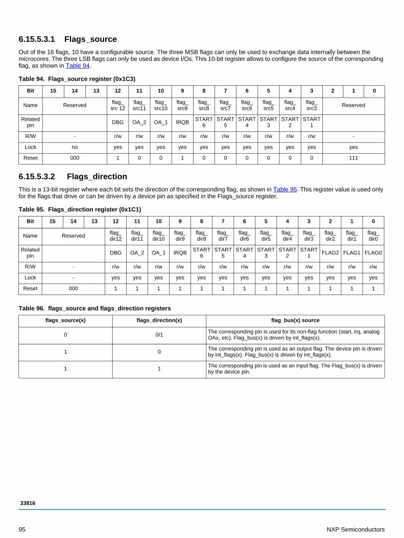
6.15.5.3.1 Flags_source
Out of the 16 flags, 10 have a configurable source. The three MSB flags can only be used to exchange data internally between the microcores. The three LSB flags can only be used as device I/Os. This 10-bit register allows to configure the source of the corresponding flag, as shown in Table 94.
6.15.5.3.2 Flags_direction
This is a 13-bit register where each bit sets the direction of the corresponding flag, as shown in Table 95. This register value is used only for the flags that drive or can be driven by a device pin as specified in the Flags_source register.
Table 94. Flags_source register (0x1C3)
Bit 15 14 13 12 11 10 9 8 7 6 5 4 3 2 1 0
Name Reservedflag_
src 12flag_src11
flag_src10
flag_src9
flag_src8
flag_src7
flag_src6
flag_src5
flag_src4
flag_src3
Reserved
Related pin
DBG OA_2 OA_1 IRQBSTART
6START
5START
4START
3START
2START
1
R/W - r/w r/w r/w r/w r/w r/w r/w r/w r/w r/w -
Lock no yes yes yes yes yes yes yes yes yes yes yes
Reset 000 1 0 0 1 0 0 0 0 0 0 111
Table 95. Flags_direction register (0x1C1)
Bit 15 14 13 12 11 10 9 8 7 6 5 4 3 2 1 0
Name Reservedflag_dir12
flag_dir11
flag_dir10
flag_dir9
flag_dir8
flag_dir7
flag_dir6
flag_dir5
flag_dir4
flag_dir3
flag_dir2
flag_dir1
flag_dir0
Related pin
DBG OA_2 OA_1 IRQBSTART
6START
5START
4START
3START
2START
1FLAG2 FLAG1 FLAG0
R/W - r/w r/w r/w r/w r/w r/w r/w r/w r/w r/w r/w r/w r/w
Lock - yes yes yes yes yes yes yes yes yes yes yes yes yes
Reset 000 1 1 1 1 1 1 1 1 1 1 1 1 1
Table 96. flags_source and flags_direction registers
flags_source(x) flags_direction(x) flag_bus(x) source
0 0/1The corresponding pin is used for its non-flag function (start, irq, analog OAx, etc). Flag_bus(x) is driven by int_flags(x).
1 0The corresponding pin is used as an output flag. The device pin is driven by int_flags(x). Flag_bus(x) is driven by int_flags(x).
1 1The corresponding pin is used as an input flag. The Flag_bus(x) is driven by the device pin.
95 NXP Semiconductors
33816

6.15.5.3.3 Flags_polarity
This is a 13-bit register where each bit sets the polarity of the corresponding flag, as shown in Table 97. The corresponding flag is inverted if a 1 is set. The value of this register is used only for the flags which are driven by or drive a device pin as specified in the flags_source register.
Some bits of this register are used to set the polarity of the start pins when they are not used as flag I/O.
6.15.5.4 Irq_handle block
This block combines all requests to issue an interrupt request on the external IRQB pin.When one of the possible irq sources request an interrupt, the IRQB pin is asserted (driven low). Meanwhile, the Interrupt_status register (0x1D4) latches the status of all the irq sources. If the IRQB pin is already asserted, further interrupt requests do not change the value of the Interrupt_status register (0x1D4). By reading this register through the SPI, it is possible to ascertain the cause of the interrupt request. When none of the possible sources is requesting an interrupt, the IRQB pin is de-asserted and the Interrupt _reg register is cleared.The possible sources are:
• one of the four microcores of the microcode requests an interrupt. The interrupt source can be configured through the Sw_interrupt_routine_addr registers (0x10E and 0x12E). The related status is reported in the Uc0_irq_status registers (0x10F and 0x12F) and in the Uc1_irq_status registers (0x110 and 0x130)
• the driver enable block disabling the output drivers. The interrupt source can be configured through the Driver_config register (0x1C5). The related status is reported in the Driver_status register (0x1D2)
• an error that occurs on the SPI interface. The interrupt source can be configured through the SPI_config register (0x1C8). The related status is reported in the SPI_error register (0x1D3)
Table 97. Flags_polarity register (0x1C2)
Bit 15 14 13 12 11 10 9 8 7 6 5 4 3 2 1 0
Name Reservedflag_
pol_12flag_
pol_11flag_
pol_10flag_pol_9
flag_pol_8
flag_pol_7
flag_pol_6
flag_pol_5
flag_pol_4
flag_pol_3
flag_pol_2
flag_pol_1
flag_pol_0
Related pin
DBG OA_2 OA_1 IRQBSTART
6START
5START
4START
3START
2START
1FLAG2 FLAG1 FLAG0
R/W - r/w r/w r/w r/w r/w r/w r/w r/w r/w r/w r/w r/w r/w
Lock - yes yes yes yes yes yes yes yes yes yes yes yes yes
Reset 000 0 0 0 0 0 0 0 0 0 0 0 0 0
Table 98. Flags_polarity
flags_polarity(x) flags_bus(x) condition
0 direct
1 inverted
Table 99. Flag_polarity register for STARTx pins not used as I/Os (0x1C2)
Bit 15 14 13 12 11 10 9 8 7 6 5 4 3 2 1 0
Name Reserved - - - -start_pol6
start_pol5
start_pol4
start_pol3
start_pol2
start_pol1
- - -
R/W - - - - - r/w r/w r/w r/w r/w r/w - - -
Lock - - - - - yes yes yes yes yes yes - - -
Reset 000 0 0 0 0 0 0 0 0 0 0 0 0 0
Table 100. Start_polarity
flags_polarity(x) flags_bus(x) condition
0 Start active high
1 Start active Low
NXP Semiconductors 96
33816

• the loss of the external clock. For more details, refer to the Clock_manager block section. The interrupt source can be configured through the Backup_clock_status_reg register (0x1C7). The related status is reported in the same register
• the signature unit of one of the two channels, in case of a wrong signature. The interrupt source can be configured through the Flash_enable registers (0x100 and 0x120). The related status is reported in the same.
6.15.5.4.1 Interrupt register
This register latches:• the status of all the interrupt request towards the external microcontroller• the halt signal generated by the automatic diagnosis towards the four microcores
The Figure 27 provides an overview of way configure and handle the interrupts according to the registers.
Table 101. Interrupt_status register (0x1D4)
Bit 15 14 13 12 11 10 9 8 7 6 5 4 3 2 1 0
Name Reservedchecksum_ch
2
checksum_ch
1
cksys_missing
SPI_irq drv_irqirq_uc1
_ch2irq_uc0
_ch2irq_uc1
_ch1irq_uc0
_ch1halt_uc1_ch2
halt_uc0_ch2
halt_uc1_ch1
halt_uc0_ch1
R/W - r r r r r r r r r r r r r
Lock no no no no no no no no no no no no no no
Reset 000 0 0 0 0 0 0 0 0 0 0 0 0 0
Table 102. Interrupt register bit description
Bit Name Function
halt_uc0_ch1 ‘1’ if the automatic diagnosis has detected a short-circuit on uc0 ch1
halt_uc1_ch1 ‘1’ if the automatic diagnosis has detected a short-circuit on uc1 ch1
halt_uc0_ch2 ‘1’ if the automatic diagnosis has detected a short-circuit on uc0 ch2
halt_uc1_ch2 ‘1’ if the automatic diagnosis has detected a short-circuit on uc1 ch2
irq_uc0_ch1 ‘1’ if the microcode of uc0 ch1 has asserted its interrupt request
irq_uc1_ch1 ‘1’ if the microcode of uc1 ch1 has asserted its interrupt request
irq_uc0_ch2 ‘1’ if the microcode of uc0 ch2 has asserted its interrupt request
irq_uc1_ch2 ‘1’ if the microcode of uc1 ch2 has asserted its interrupt request
drv_irq ‘1’ if the driver status block has disabled the output drivers
SPI_irq ‘1’ if the SPI interface has detected an error on the SPI communication
cksys_missing ‘1’ if the clock monitor has detected a cksys missing condition
checksum_ch1 ‘1’ if the checksum of the code RAM of ch1 is wrong
checksum_ch2 ‘1’ if the checksum of the code RAM of ch2 is wrong
97 NXP Semiconductors
33816

Figure 27. Interrupts sources configuration and handling overview
NXP Semiconductors 98
33816

6.15.5.5 Backup_clock_status_handle block
This block contains an 8-bit register (Backup_clock_status_reg register) that handles the loss of its input clock reference.
The 8-bit register provides clock signal status monitoring to the external microcontroller. This is done by latching the information where a switch to the backup_reference signal has occurred:
• timing_violation: this bit is set if a timing violation has been detected. Writing a ‘1’ value on this register bit, resets the timing violation information.
• loss_of_clock: this read-only bit (loss_of_clock) latches the condition when the input reference is missing. These conditions are described in the PLL and Backup Clock section. The loss_of_clock bit can be reset by applying a valid clock frequency to the CLK device pin and setting the switch to clock pin bit high.
• switch_to_clock_pin: this bit (active on rising edge) provides a way to reset the loss of clock condition. If this bit is set during a loss of clock condition, it is reset as soon as the clock manager switches the PLL input to the external reference. If this bit is set while there is no loss of clock, the bit is reset immediately without any effect.
• mcu_irq_en: this bit generates an interrupt request to the microcontroller when cksys missing is detected. This interrupt is active until this register is read.
• uc0_ch1_irq_en: this bit enables the generation of an interrupt request to microcore 0 channel 1 when cksys missing is detected.• uc1_ch1_irq_en: this bit enables the generation of an interrupt request to microcore 1 channel 1 when cksys missing is detected.• uc0_ch2_irq_en: this bit enables the generation of an interrupt request to microcore 0 channel 2 when cksys missing is detected.• uc1_ch2_irq_en: this bit enables the generation of an interrupt request to microcore 1 channel 2 when cksys missing is detected.• cksys_missing_disable_driver: if this bit is set, the output drivers are disabled via the signal cksys_drven, as long as the
cksys_missing signal is ‘1’, for a typical duration of 25 s, as defined by tPLL_RELOCK.
The interrupt to the external microcontroller and to the microcores is triggered as long as the cksys_missing signal is set. The microcore is able to process the interrupt as soon as there is a valid clock signal available on the CLK pin. The interrupt is triggered every time the Clock_manager switches to the internal clock reference, and when the clock manager tries to switch back to the external clock reference as this action is requested via the SPI.
6.15.5.6 Cipher_unit block
This block has the function to secure the code downloaded by the microcontroller into the Code RAM via the SPI. The data loaded at device startup must be encrypted with the suitable cipher. This block receives an encoded SPI stream and decodes it at runtime. The decoded microcode is then stored in the Code RAM. This feature cannot be disabled.The cipher algorithm is re-initialized every time the code memory is selected by a write operation to the Selection register (0x3FF).
6.15.5.7 Communication_interface block
The access to memories and register is managed, paging the addresses through a SPI accessible register, named Selection_reg.
Table 103. Backup_clock_status_reg register (0x1C7)
Bit 15 14 13 12 11 10 9 8 7 6 5 4 3 2 1 0
Name -timing_violation
cksys_missing_disable_
driver
uc1_ch2_
irq_en
uc0_ch2_
irq_en
uc1_ch1_
irq_en
uc0_ch1_
irq_en
mcu_irq_en
switch_to_
clock_pin
loss_of_
clock
R/W - r/w r/w r/w r/w r/w r/w r/w r/w r
Lock - no yes yes yes yes yes yes no no
Reset - 0 0 0 0 0 0 0 0 0
99 NXP Semiconductors
33816

6.15.5.7.1 Selection_reg register
The selection register is a 3-bit register aimed to select before starting the read/write operations toward a given address, which internal Code RAM is accessed, or to select all the other addresses, including the two Data RAMs and all the registers.
Table 105 details the meaning of the three bits in this register. Some bit combinations are not allowed in this register and is ignored.
This selection register is a unique register that is accessed from the SPI, whatever the value of the selection register. The two Code RAMs can be written in parallel during Normal mode.Based on the values of the address bus (a_bus) and the selection register, the communication_interface block generates the address map of the device. This is achieved through the following signals working as chip selects for all the addressing areas of the component as detailed in Table 106.
Table 104. Selection_reg register (0x3FF)
Bit 15 14 13 12 11 10 9 8 7 6 5 4 3 2 1 0
Name Reservedcomm_page_s
el
CRAM_ch2_s
el
CRAM_ch1_s
el
R/W - r/w r/w r/w
Lock - no no no
Reset 0000000000000 0 0 0
Table 105. Selection register
Selection register (MSB to LSB) Enablement address
000 No page selected. Further SPI operation is ignored, except for the one concerning this register.
001 Channel 1 Code RAM selected.
010 Channel 2 Code RAM selected.
011 Write operation affects both channel’s Code RAM. Read operation is not possible in this case.
100 Common page selected
101
The two LSB are ignored. ’100’ is written to the register. Common page selected.110
111
Table 106. Map areas selection
Chip select Area addressed
ch_sel_1(0) Data RAM of channel 1
ch_sel_1(1) Code RAM of channel 1
ch_sel_1(2) Configuration registers of channel 1
ch_sel_2(0) Data RAM of channel 2
ch_sel_2(1) Code RAM of channel 2
ch_sel_2(2) Configuration registers of channel 2
ext_sel_mcr Main configuration register: all the generic registers located in the channel_management block
ext_sel_io I/O configuration registers
ext_sel_diag Diagnosis configuration registers
NXP Semiconductors 100
33816

6.15.5.8 Prescalers block
This block contains all the clock dividers available in the 33816. The divider ratios can be set in the Ck_pre register via the SPI.
6.15.5.8.1 Clock prescaler
This 6-bit register sets the divider ratio to generate the ck clock, based on the cksys clock signal. This clock feeds the two act_channel blocks registers, except those accessible with the SPI, which directly clocked by cksys.fCK = fCKSYS/(ck_per + 1) = 1/tCK
Note that the actual divider ratio is ck_per + 1. Setting ck_per to ’000100’ ck is cksys/5.
The different device/channel operating mode available according to the Ck_per setting are described in Table 108.
6.15.5.8.2 Clock offset compensation prescaler
This 8-bit register sets the divider ratio to generate the ck_ofscomp clock, based on the cksys clock signal. This clock feeds the offset recovery counters of the current measure interface.Note that the actual divider ratio is ck_ofscmp_per + 1. Setting ck_ofscmp_per to ’00001000’ ck_ofscomp is cksys/9.
Table 107. Ck_per register (0x1C0)
Bit 15 14 13 12 11 10 9 8 7 6 5 4 3 2 1 0
Name Reserved ck_per
R/W - r/w
Lock - yes
Reset 0000000000 000000
Table 108. Ck_per and device modes
Ck_per Clock dividerRead and write SPI access to registers
and DRAMSingle microcore Dual microcore
Drive outputs from flag pins
0 1 yes no no no
1 2 yes yes no yes
2 3 yes yes no yes
3 4 yes yes yes yes
Table 109. Ck_ofscomp_per register (0x1C4)
Bit 15 14 13 12 11 10 9 8 7 6 5 4 3 2 1 0
Name Reserved ck_ofscmp_per
R/W - r/w
Lock - yes
Reset 00000000 0000000
101 NXP Semiconductors
33816

6.15.5.9 Driver_enable block
This block generates the enable signal to the output drivers (signal en_hs for the high-side drivers, and en_ls for the low-side drivers). The conditions described below must be considered to enable the drivers. Some of them are mandatory and others are configurable through the Backup_clock_status_reg (0x1C7) and the Driver_config (0x1C5) registers.The low-side one to six output drivers are enabled when:
• cksys_drven = 1 – The input clock signal is not missing (configurable)• drv_en = 1 – The DRVEN pin is high (mandatory)• uv_vccp = 0 – There is not undervoltage on VCCP (mandatory)• uv_vcc5 = 0 – There is not undervoltage on VCC5 (mandatory)
The low-side seven output driver is enabled when:• cksys_drven = 1 – The input clock signal is not missing (configurable)• drv_en = 1 – The DRVEN pin is high (configurable)• uv_vccp = 0 – There is not undervoltage on VCCP (mandatory)• uv_vcc5 = 0 – There is not undervoltage on VCC5 (mandatory)
The high-side output drivers are enabled when:• cksys_drven = 1 – The input clock signal is not missing (configurable)• drv_en = 1 – The DRVEN pin is high (mandatory)• uv_vccp = 0 – There is not undervoltage on VCCP (mandatory)• uv_vcc5 = 0 – There is not undervoltage on VCC5 (mandatory)• uv_vboost = 0 - There is not undervoltage on VBOOST (configurable)
6.15.5.9.1 Driver status
This 7-bit register provides a monitoring of the output drivers status to the external microcontroller. This is done by latching any error condition which disables the output drivers. Some of these error conditions must be enabled through the Backup_clock_status_reg (0x1C7) and the Driver_config registers (0x1C5).
cksys_missing: this bit is set if the cksys missing condition of the clock_manager block disables the drivers. This condition can be configured in the Backup_clock_status_reg register (0x1C7).DrvEn_latch: this bit latches the condition when the DRVEN input pin is inactive.
• 1: DRVEN pin was NOT low since last reset of the driver_status register• 0: DRVEN pin was low since the last reset of the driver_status register
DrvEn_value: this bit is not an error condition but only a ’living copy’ of the DRVEN pin.• 1: DRVEN pin is high• 0: DRVEN pin is low
over_temp: this bit latches the condition that an overtemperature is present. It is not used to disable the drivers.uv_vboost: this bit is set if the undervoltage on the vboost disables the high-side drivers. This condition can be configured through the Driver_config register (0x1C5).uv_vcc5: this bit latches the undervoltage condition on VCC5.uv_vccp: this bit latches the undervoltage condition on VCCP or the error issued from GND loss detection.Once an error bit has been set, it can only be reset by a SPI write operation in this register, considering that the corresponding error is no longer present. The same error bits are reset even upon SPI read operations, but only when a proper enable bit is set in the Reset_behavior register (0x1CE).
Table 110. Driver_status register (0x1D2)
Bit 15 14 13 12 11 10 9 8 7 6 5 4 3 2 1 0
Name Reservedcksys_missing
DrvEn_latch
DrvEn_value
over_temp
uv_boost
uv_vcc5
uv_vccp
R/W - r r r r r r r
Lock - no no no no no no no
Reset on read
conf. conf. no conf. conf. conf. conf.
Reset 0000000 0 1 - 0 0 0 0
NXP Semiconductors 102
33816

6.15.5.9.2 Driver configuration
This register allows to configure the conditions leading to the driver disable and to the interrupt generation. The interrupt request generation towards the microcontroller and the microcores can also be set.
The driver_enable block generates a local interrupt masking the five possible disable conditions through the bits detailed below:• drv_en_irq_en: if set, the drv_en generates the local interrupt.• vboost_irq_en: if set, an undervoltage on VBOOST generates the local interrupt.• vcc5_irq_en: if set, an undervoltage on VCC5 generates the local interrupt.• vccp_irq_en: if set, an undervoltage on VCCP generates the local interrupt.• over_temp_irq_en: if set, the overtemperature condition generates the local interrupt.
If a local interrupt is generated, it is possible to propagate it to an external device (microcontroller) and to the four microcores. This is done when the following bits are set:
• irq_mcu_en, for the external device through the IRQB pin• irq_uc0_ch1_en, for the microcore 0 of channel 1• irq_uc1_ch1_en, for the microcore 1 of channel 1• irq_uc0_ch2_en, for the microcore 0 of channel 2• irq_uc1 ch2 en, for the microcore 1 of channel 2
This register contains some other configuration bit related to the output drivers:• iret_en: the driver_enable block automatically generates a return from interrupt request towards all the microcores. This request
can be filtered by microcode if not required. Two kind of return from interrupt is selectable. If iret_en is set to ‘0’, a return from interrupt request is sent to the microcores when the drivers are re-enabled after a disable condition. If iret en is set to ‘1’, a return from interrupt request is sent to the microcores when the Drivers_status register (0x1D2) is cleared. For the return from interrupt to happen the driver status register must be write or read while the reset on read configuration is activated in the Reset_behavior register (0x1CE)
• vboost_disable_en: if set, an undervoltage of VBOOST disables the output drivers.• vboost_mon_en: this signal configures the divider on the VBOOST voltage. If vboost_mon_en is set to ‘0’, VBOOST is divided by 32
and then compared with a threshold. If vboost_mon_en is set to ‘1’, VBOOST is divided by 4 and then compared with a threshold.• ls7_ovr: if set to ‘1’, the low-side seven output driver is not influenced by the DrvEn signal.• hs5_ls36_ovr: if set to ‘1’, the high-side five and low-side three and six output driver is not influenced by the DrvEn signal.• vccp_ext_en: if set to ‘0’, the internal voltage regulator is enabled and the corresponding pin is used only to connect a bypass
capacitor. If set to ‘1’, the internal voltage regulator is disabled and the VCCP voltage must be supplied externally through the corresponding pin. During bootstrap switch init (refer to Bootstrap switch control section) this setting is bypassed and the value of the vccp_ext_enable signal is set to the inverted value of the DBG pin sampled at reset (POResetB and ResetB) (see Table 112 for more details). In this case, the DBG pin, at reset, needs to be configured as an input, whose value is latched at the rising edge of the POResetB and ResetB signal, and used to set the configuration of the VCCP internal regulator during the init phase of the bootstrap switch. A SPI reset leaves the latched information unchanged. The DBG pin has an internal weak pull-up resistor so its value is ‘1’ when not connected (n. c.).
The different device/channel operating mode available according to the Ck_per setting are described in Table 112.
Table 111. Driver_config register (0x1C5)
Bit 15 14 13 12 11 10 9 8 7 6 5 4 3 2 1 0
Namehs5_ls36_ovr
vccp_ext_en
ls7_ovr
vboost_mon_en
vboost_disable
_en
over_temp_irq_en
drv_en_irq_
en
vboost_irq_
en
vcc5_irq_en
vccp_irq_en
iret_en
irq_uc1_ch2_en
irq_uc0_ch2_en
irq_uc1_ch1_en
irq_uc0_ch1_en
irq_mcu_
en
R/W r/w r/w r/w r/w r/w r/w r/w r/w r/w r/w r/w r/w r/w r/w r/w r/w
Lock yes yes yes yes yes yes yes yes yes yes yes yes yes yes yes yes
Reset 0 1 1 0 0 0 0 0 0 0 0 0 0 0 0 0
103 NXP Semiconductors
33816

6.15.5.10 SPI_access_controller block
All the SPI accessible registers can be accessed also by the microcores through a ’SPI backdoor’. However, Data and Code RAMs are unavailable through the backdoor. The SPI_access_controller block receives all the register read/write requests, from the SPI interface and from all the enabled microcores.The requests coming from the SPI interface are considered with the highest priority. When these requests are received, the requested operation (register read/write) is immediately performed.All the requests from the microcores are performed before the end of the next ck clock cycle (the clock cycle used for the microcode execution). It means that the result of the operation is available for the second instruction after the read/write request. The value of the SPI backdoor registers must not be changed until the backdoor operation is finished.
6.15.5.11 Trace_unit block
The step by step evolution of the code execution for all the microcores can be traced throughout the DBG pin. This allows obtaining the microprogram counter values of the microcores in real time: the microprogram counter value (uPC) corresponds to the address of the instruction being executed.To allow tracing, the DBG pin is used as an asynchronous serial line running at the cksys clock frequency. The device translates the data into microprogram counter values. The value is transmitted back, thanks to the tracer function through the DBG pin.If the clock prescaler (refer to Ck_per (0x1C0) section for more details) is set to three, full trace mode is enabled whatever the value of PLL_factor bit in the register (PLL_config (0x1C6). For all other clock prescaler values, the trace mode doesn’t work properly (clock prescaler > 3) or is not available (clock prescaler < 3). The MSB is always transmitted first on the DBG pin.
6.15.5.11.1 Full trace mode
Considering a point in the code execution, there are a very limited number of possibilities for the next values of the microprogram counter. Trace is then implemented, such as to transmit a code on four bits issued for the microprogram counter values.The trace operation consists of reconstructing the execution path from the codes that the device transmits to the tracer. However, these codes only describe variation of the uPC value. To obtain the actual execution path, the trace operation must start from a point in the code known by the tracer. From the starting point and knowing all the variations, it is possible to obtain the uPC path.The trace can be activated on one microcore at a time.The trace sequence is composed of five steps:
1. Calibrate: The communication between the 33816 and the tracer is asynchronous, since no clock line is shared. The first frame transmitted through the DBG pin is a burst of eight clock cycles with a frequency half of the internal cksys.
At the end of this phase the DBG pin stays low for at least one ck clock period.
2. Sync: The sync point is specified in Trace_start register (0x1CA). If the trace operation is enabled in the Trace_config register (0x1CC) and the trace unit is in idle state, when the uPC value of the selected microcore reaches the sync point, the 4 bits code ’1010’ (start sync) is transmitted on the DBG pin.
Then the trace_unit goes to the next phase.
3. Trace: Each cycle is transmitted a four bit code value that identifies which path has been taken by the code execution among possible ones. Due to the many possible paths, to keep the number of codes to 14 (‘0000’ and ‘1111’ are not used because they are difficult to handle in an asynchronous communication), some codes have different meaning according to which instruction is being executed. Some codes have different meaning if you are executing normal code or if you are inside an interrupt service routine (ISR).
Table 112. VCCP external enable setting
DBG pin (latched) SPI bitBooststrap init
(Min. 1 HS)VCCP external supply enablement
1 (n.c.) - 1 0 (Internal regulator)
1 (n.c.) 1 1 1 (External VCCP supply)
1 (n.c.) 0 0 0 (Internal regulator)
0 1 - 1 (External VCCP supply)
0 0 - 0 (Internal regulator)
NXP Semiconductors 104
33816

6.15.5.11.2 Normal execution trace
The codes used during normal execution are the following:• Code ’0101’, default path taken. It means that the path taken after the current instruction is the default one. For nearly all instructions,
it means that the instruction has not altered the code flow, no interrupt has been received, so the following instruction is the next one. However their are some exceptions:
• Unconditional jumps (jmpr, jmpf) and software interrupt requests (reqi) cannot produce this code.• This code is produced by the wait instruction if the wait is fulfilled and the wait entry 1 is selected as next destination.
• Code ’1010’, forked path taken. It means that the instruction has altered the code execution path. It also means that no hardware interrupt has been received. The new uprogram counter value depends on the exact instruction that is currently under execution. For this reason, the tracer device must be provided with the microcode, to correctly select the new uPC value.
Only some instruction can produce this code:• The wait instruction produces this code when the uprogram counter is unchanged (the code is waiting).• All the jump instructions produce this code when the jump is taken.• The jump to subroutine instructions (jtsr, jtsf) always produce this code.• The software interrupt request instruction (reqi) always produces this code.
• Code ’0100’, automatic diagnosis interrupt. It means that the code execution has been interrupted for a fault detected by the automatic diagnosis. The new uprogram counter value is the start of the diagnosis interrupt routine. The tracer must be aware of the interrupt table to correctly select the new uPC value.
• Code ’0010’, driver disabled interrupt. It means that the code execution has been interrupted for a fault that leads to disable the output drivers.
The new uprogram counter value is the start of the driver disabled interrupt routine. The tracer must be aware of the interrupt table to correctly select the new uPC value.• Code ’0011’, start edge interrupt. It means that the code execution has been interrupted by a software interrupt caused by a start edge
(Refer to Sw_interrupt_routine_addr (0x10E, 0x12E) for configuration). The new uprogram counter value is the start of the software interrupt routine. The tracer must be aware of the interrupt table to correctly select the new uPC value.
• Code ’0110’, wait entry 2 selected. This code can be produced only by the wait instruction (wait) if the wait is fulfilled and the wait entry 2 is selected as next destination.
• Code ’1011’, wait entry 3 selected. This code can be produced only by the wait instruction (wait) if the wait is fulfilled and the wait entry 3 is selected as next destination.
• Code ’1101’, wait entry 4 selected. This code can be produced only by the wait instruction (wait) if the wait is fulfilled and the wait entry 4 is selected as next destination.
• Code ’1001’, wait entry 5 selected. This code can be produced only by the wait instruction (wait) if the wait is fulfilled and the wait entry 5 is selected as next destination.
6.15.5.11.3 Interrupt execution trace
The most difficult concept is how to trace the flow of the uPC after the exit from an interrupt routine.If execution restarts, the next uPC value is the microcore entry point (refer to Uc0_entry_point (0x10A, 0x12A) and Uc1_entry_point (0x10B, 0x12B) sections for entry point configuration).If execution continues, the last code of the ISR point to which direction the flow continues, referring to the last instruction executed before the ISR was called. The tracing is ‘broken’ if the sync point is inside the ISR routine.If the execution restarts, after the ISR or the sync point is during normal code or inside another ISR, trace is not limited.Interrupt return (iret) instruction called with the ’restart’ parameter produces a fixed code (’1010’).Interrupt return (iret) instruction called with the ’continue’ parameter can produce any of the codes used during normal execution, except the codes referring to interrupt requests (’0010’, ’0011’ and ’0100’). Using the same rules, this code point to the path selected by the last instruction before the ISR.Automatic interrupt return request have the same possible destinations as the interrupt return (iret) instruction called with the ’continue’ parameter. However in this case, the codes are different from the ones used during normal execution.• Code ’0101’, default path taken. It means that the path taken after the current instruction is the default one. For nearly all instructions
it means that the instruction has not altered the code flow, no interrupt has been received, so the following instruction is the next one.
The are some exceptions:• Unconditional jumps (jmpr, jmpf) cannot produce this code.• Interrupt return (ret) instruction produces this code when they have the ’continue’ parameter and the path to be taken after the ISR
is the default one (includes wait entry 1 selected).
105 NXP Semiconductors
33816

This code is produced by the wait instruction (wait) if the wait is fulfilled and the wait entry 1 is selected as next destination.• Code ’1010’, forked path taken. It means that the instruction has altered the code execution path. It also means that no hardware
interrupt has been received. The new microprogram counter value depends on the exact instruction that is currently under execution. For this reason, the tracer device must be provided with the microcode to correctly select the new uPC value.
Only some instruction can produce this code:• Interrupt return (iret) instruction produces this code when they have the ’restart’ parameter.• Interrupt return (iret) instruction produces this code when they have the ’continue’ parameter and the path to be taken after the ISR
is the forked one.• The wait instruction produces this code when the uprogram counter is unchanged (the code is waiting).• All the jump instructions produce this code when the jump is taken.• The jump to subroutine instructions (jtsr, jtsf) always produce this code.
• Code ’0110’, wait entry 2 selected. This code can be produced by the wait instruction (wait) if the wait is fulfilled and the wait entry 2 is selected as next destination. It is also produced by the interrupt return (iret) instruction when they have the ’continue’ parameter, a wait instruction was executing when ISR was called and the destination 2 was about to be selected.
• Code ’1011’, wait entry 3 selected. This code can be produced by the wait instruction (wait) if the wait is fulfilled and the wait entry 3 is selected as next destination. It is also produced by the interrupt return (iret) instruction when they have the ’continue’ parameter, a wait instruction was executing when ISR was called and the destination 3 was about to be selected.
• Code ’1101’, wait entry 4 selected. This code can be produced by the wait instruction (wait) if the wait is fulfilled and the wait entry 4 is selected as next destination. It is also produced by the interrupt return (iret) instruction when they have the ’continue’ parameter, a wait instruction was executing when ISR was called and the destination 4 was about to be selected.
• Code ’1001’, wait entry 5 selected. This code can be produced by the wait instruction (wait) if the wait is fulfilled and the wait entry 5 is selected as next destination. It is also produced by the interrupt return (iret) instruction when they have the ’continue’ parameter, a wait instruction was executing when ISR was called and the destination 5 was about to be selected.
• Code ’0001’, forked path after automatic interrupt return. This code can be produce only when an automatic interrupt return is received and the path to be taken after the ISR is the forked one.
• Code ’0111’, default path after automatic interrupt return. This code can be produced when an automatic interrupt return is received and the path to be taken after the ISR is the default one (includes wait entry 1 selected).
• Code ’0100’, wait entry 2 selected after automatic interrupt return. This code can be produce only when an automatic interrupt return is received, a wait instruction was executing when ISR was called and the destination 2 was about to be selected.
• Code ’0010’, wait entry 3 selected after automatic interrupt return. This code can be produce only when an automatic interrupt return is received, a wait instruction was executing when ISR was called and the destination 3 was about to be selected.
• Code ’1110’, wait entry 4 selected after automatic interrupt return. This code can be produce only when an automatic interrupt return is received, a wait instruction was executing when ISR was called and the destination 4 was about to be selected.
• Code ’0011’, wait entry 5 selected after automatic interrupt return. This code can be produce only when an automatic interrupt return is received, a wait instruction was executing when ISR was called and the destination 5 was about to be selected.
1. Stop Sync: The trace operation is not meant to last indefinitely. It is possible to define a ’stop’ address (refer to the Trace_stop register (0x1CB) to define stop address). If during the precedent phase (trace) the uPC reaches the stop address, the code ’1100’ is sent on the DBG pin and the trace_unit goes to the following phase.
2. Post Trigger: The trace operation continues for a fixed number of ck clock cycles. After this time has elapsed, the trace_unit goes to idle state.
6.15.5.11.4 Trace_start
The trigger_address field contains the address that is used to synchronize the 33816 trace_unit with the external tracer. If the trace operation is enabled (prefer to Trace_config register (0x1CC) for trace unit enablement) and the trace unit is in idle state, when the uPC value of the selected microcore reaches this address, the sync code is transmitted on the DBG pin. The trace_unit then goes to the next phase.
Table 113. Trace_start register (0x1CA)
Bit 15 14 13 12 11 10 9 8 7 6 5 4 3 2 1 0
Name Reserved start_address
R/W - r/w
Lock - no
Reset 000000 00000000000
NXP Semiconductors 106
33816

6.15.5.11.5 Trace_stop
The stop_address field contains the address that is used to finalize the trace operation. If the trace operation is ongoing (trace phase), when the uPC value of the selected microcore reaches this address, the stop code is transmitted on the DBG pin. Then the trace_unit goes to the next phase (post trigger phase).
6.15.5.11.6 Trace_config
• trace_enable. When this bit is set to ‘1’, the trace_unit start the first phase of the trace operation. This bit can be set to ‘0’ by the user, to immediately stop the device trace unit transmission. This bit is automatically reset after the trace operation is complete.
• uc_select. Select which is the microcore target of the trace operation:• ’00’: microcore 0, channel 1.• ’01’: microcore 1, channel 1.• ’10’: microcore 0, channel 2.• ’11’: microcore 1, channel 2.
• post_trigger_length. This field selects the duration of the post trigger phase, expressed as number of ck clock cycles. However, setting the post_trigger_length field to 255 generates a continuous stream after the stop point. The trace_unit can be simply deactivated by writing ’0’ in the trace_enable bit.
6.15.5.12 SPI_interface_slave block
'The communication between the 33816 and the main microcontroller is managed with a 16-bit SPI interface. This block includes four sub-blocks meant to control the SPI transfer:
• spi_interface_slave• spi_config• spi_protocol• spi_error
Table 114. Trace_stop register (0x1CB)
Bit 15 14 13 12 11 10 9 8 7 6 5 4 3 2 1 0
Name Reserved stop_address
R/W - r/w
Lock - no
Reset 0 0
Table 115. Trace_config register (0x1CC)
Bit 15 14 13 12 11 10 9 8 7 6 5 4 3 2 1 0
Name ReservedTrace enable
uc_select post_trigger_length
R/W - r/w r/w r/w
Lock - no no no
Reset 00000 0 00 00000000
107 NXP Semiconductors
33816

Figure 28. Spi_interface_slave block diagram
6.15.5.12.1 Spi_interface_slave block
This block is the module providing the SPI connection features. It only works as a slave SPI module, allowing only 1- bit data transactions. The device requires a cphase value of 1 and a cpol value of 0. This means that the SPI module samples the MOSI signal, during write operations on the falling edge of the serial clock sclk. Likewise, during read operations, the SPI module always puts the output value available on the MISO signal on the rising edge of the sclk clock. The cpol value of ‘1’ can be implemented by adding an external inverter.
6.15.5.12.2 Spi_config block
The spi_config register is an 8-bit register storing the SPI protocol configuration and SPI diagnosis.
• miso_slewrate: selects one of the two possible values for the slew rate of the MISO pin.• protocol_mode: select the type of burst transmission accepted by the protocol, ‘0’ means mode A, ‘1’ means mode B.• irq_en: enable the SPI interface to request an interrupt towards the microcontroller, in case an incorrect SPI transmission is received.• watchdog: when using mode A, the maximum time the SPI chip select can be inactive during a burst is expressed as follows:
• tWATCHDOG = tCKSYS ((watchdog +1) * 32768)
where tCKSYS is the period of the cksys internal clock.The SPI protocol mode can be selected through the SPI. In this case, the SPI transmission must be compatible to mode A and B (see SPI read access and Mode B section for A and B compatible protocol description). The number of operations for the SPI transmission cannot be ‘0’ and the chip select must not be deassert during the transmission.The protocol mode can be changed at any time.
6.15.5.13 Spi_protocol block
The spi_protocol block allows managing the location where the incoming data from the SPI_interface is stored. It also routes the path that is used to access data when a SPI reading is requested. After reset and after SPI transmission is completed, the protocol always waits for the16-bit control word.
Table 116. Spi_config register (0x1C8)
Bit 15 14 13 12 11 10 9 8 7 6 5 4 3 2 1 0
Name Reservedmiso_
slewrate
protocol_
modeirq_en watchdog
R/W - r/w r/w r/w r/w
Lock - yes yes yes yes
Reset 0 0 0 0 01010
NXP Semiconductors 108
33816

The field ‘r_w’ defines if the action is to read data (r_w = ‘1’) through the SPI or write (r_w = ‘0’) incoming data in registers.The field ‘number’ defines the number of 16-bit words read or written by the external microcontroller. The offset value is limited to a maximum of 31 words. The field ‘offset’ defines where the read or write operation must start so what the first address in this burst of operations to be accessed.To detect corrupted burst of data, the protocol monitors the burst, according to the ‘protocol mode’ bit of the SPI_config Register (0x1C8).
6.15.5.13.1 SPI read access
A SPI frame for read access consists of 2 to 32 16-bit words. The way the number of words is defined depends on the SPI mode used (A or B). The table below shows the data transmitted on MOSI and MISO. During the command word the check byte and the SPI error status is transmitted via the MISO line.The MSB is always transmitted first.
Table 117. SPI control word description
Control word area Description
Control_word [15] r_w: read (1)/write (0) operations
Control_word [14:5] offset: start address
Control_word [4:0] number: number of operations
Table 118. SPI read access
MOSI word 1 (control word) – read access
Bit 15 14 13 12 11 10 9 8 7 6 5 4 3 2 1 0
Name r_w offset number
Value 1 0 to 1023 n=0 to 31
MISO word 1 (control word) – read access
Bit 15 14 13 12 11 10 9 8 7 6 5 4 3 2 1 0
Name check bytecksys
missingframe error
word error
Value 1 0 1 0 1 0 1 0 1 0 1 0 1 0 0 0
MOSI word 2 (data) – read access
Bit 15 14 13 12 11 10 9 8 7 6 5 4 3 2 1 0
Name (empty)
Value 0 0 0 0 0 0 0 0 0 0 0 0 0 0 0 0
MISO word 2 (data) – read access
Bit 15 14 13 12 11 10 9 8 7 6 5 4 3 2 1 0
Name read data 1
Value x x x x x x x x x x x x x x x x
MOSI word n+1 (data) – read access
Bit 15 14 13 12 11 10 9 8 7 6 5 4 3 2 1 0
Name (empty)
Value 0 0 0 0 0 0 0 0 0 0 0 0 0 0 0 0
MISO word n+1 (data) – read access
Bit 15 14 13 12 11 10 9 8 7 6 5 4 3 2 1 0
Name read data n
Value x x x x x x x x x x x x x x x x
109 NXP Semiconductors
33816

6.15.5.13.2 SPI write access
A SPI frame for write access consists of 2 to 32 16-bit words. The way the number of words is defined depends on the SPI mode used (A or B). the table below shows the data transmitted on MOSI and MISO. During the command word and all data words the check byte and the SPI error status is transmitted via the MISO line. The MSB is always transmitted first.
Table 119. SPI write access
MOSI word 1 (control word) – write access
Bit 15 14 13 12 11 10 9 8 7 6 5 4 3 2 1 0
Name r_w offset number
Value 0 0 to 1023 n=0 to 31
MISO word 1 (control word) – write access
Bit 15 14 13 12 11 10 9 8 7 6 5 4 3 2 1 0
Name check bytecksys
missingframe error
word error
Value 1 0 1 0 1 0 1 0 1 0 1 0 1 0 0 0
MOSI word 2 (data) – write access
Bit 15 14 13 12 11 10 9 8 7 6 5 4 3 2 1 0
Name write data 1
Value 0 0 0 0 0 0 0 0 0 0 0 0 0 0 0 0
MISO word 2 (data) – write access
Bit 15 14 13 12 11 10 9 8 7 6 5 4 3 2 1 0
Name check bytecksys
missingframe error
word error
Value 1 0 1 0 1 0 1 0 1 0 1 0 1 0 0 0
MOSI word n+1 (data) – write access
Bit 15 14 13 12 11 10 9 8 7 6 5 4 3 2 1 0
Name write data n
Value 0 0 0 0 0 0 0 0 0 0 0 0 0 0 0 0
MISO word n+1 (data) – write access
Bit 15 14 13 12 11 10 9 8 7 6 5 4 3 2 1 0
Name check bytecksys
missingframe error
word error
Value 1 0 1 0 1 0 1 0 1 0 1 0 1 0 0 0
NXP Semiconductors 110
33816

6.15.5.14 Mode A
Figure 29. SPI protocol mode A
The maximum delay between data belonging to the same frame is specified by the spi_watchdog parameter bits of the Spi_config register (0x1C8). Between one data transfer and the next, the SPI chip select can be asserted on not. If this delay exceeds the watchdog time, the SPI interface goes into error state.It is possible to perform long frame transfers by sending a control word with the parameters number and offset set to zero. The effect varies according to the current value of the selection register bits defined in the Selection_reg register (0x3FF):
• if the value of the select register is ’001’, the protocol transmits a frame allowing operations starting from the address 0; the number of operations is specified by the value of the Code_width register (0x107) of channel 1. This command is used to write the whole Code RAM of channel one with only one command word.
• if the value of channel select register is ’010’, the protocol transmits a frame allowing operations starting from the address 0; the number of operations is specified by the value of the Code_width register (0x127) of channel 2. This command is used to write the whole Code RAM of channel two with only one command word.
• if the value of channel select register is ’011’, the protocol transmits a frame allowing operations starting from the address 0; the number of operations is specified by the value of the Code_width register (0x0107) of channel 1. This command is used to fully write the Code RAMs of both channel (with exactly the same code) with only one command word.
• if the value of channel select register is ’100’, the protocol transmits a frame allowing operations starting from the address 0; the maximum number of operations is 128. This command is used to fully write the Data RAMs of both channels with only one command word.
• For all the other values of channel select register, the command is ignored.
Transmission of control word with the parameter number set to zero and the parameter offset greater than zero is not allowed. It leads to data corruption in the registers or Data RAM. A SPI write access example is provided below. In this example, the used is setting the ADC conversion register 1 and 2 (0x194 and 0x195).
• The first step consists in selecting the communication interface as target. The selection is done by writing the value 0x0004 at the Selection register address (0x3FF). The first 16-bit words to be sent is ‘0_1111111111_00001’ (0x07FE1). As the device is in idle conditions, the incoming data is a command word: write operation is selected (as the MSB is ‘0’) starting from address 0x03FF (the ten offset bits) and one data word is sent in the next frame (‘00001’ written in the 5 LSB). The next incoming frame (the data word) is 0x0004. As the number of word expected arrives, the SPI block returns to idle state;
• The second step is writing the value of the two ADC conversion register one and two: the SPI block is expecting a command word. The correct data to send is ’0_0110010100_00010’. write operation is selected (as the MSB is ‘0’) starting form address 0x0194 (‘0110010100’ written in the offset field) and two data words sent in the next frame (‘00010’ written in the 5 LSB). The next incoming data is written in the ADC conversion register one (0x0194) then in following data into the ADC conversion register two (0x195).
111 NXP Semiconductors
33816

6.15.5.15 Mode B
Figure 30. SPI protocol mode B
For all the duration of data transmission, the SPI chip select must be asserted. The first word after the chip select assertion is a command word and the following ones are the data word. If the number parameter is not zero, the SPI interface goes into an error state if:
• The chip select is de-asserted and the number of words transferred is lower than the number specified in the command word,• The number of word transferred is equal to the number parameter + 1. If a write burst in mode B is longer than programmed in the
number parameter one word more is written to the memory before the error is detected.
If the number parameter is zero, the number of data word transmitted is only determined by the assertion of SPI chip select.Reading any register ’reset on read’ or any register located just before such a register using a mode B SPI communication with the number parameter set to zero is not recommended. It may lead to register reset even if no read out via the SPI. A such situation can be avoid by specifying the number data words transmitted in the command word.
6.15.5.15.1 Spi_error block
The Spi_error register is a 3-bit register split as described by the following.• cksys_missing: cksys missing error condition• frame_error: frame incomplete error condition• word_error: word incomplete error condition
The block monitors the spi_protocol and the spi_interface, and reports any errors during the communication with the microcontroller. If an error is detected, the corresponding code is stored in the SPI_error register. To warn the microcontroller, during the write transfer (from microcontroller to device), the MISO signal transfers a diagnostic word:
• the first 13 bits of this word are constant (’1010101010101’) and are used to detect short circuits on the MISO line, • the last three bits copy the three LSBs of the SPI_error register.
After an error code is written in this register, the register becomes write-protected to latch the error condition. In this case, any other error is ignored to avoid error cumulation effect issued from error source side effect.In addition, an interrupt request can be generated towards the microcontroller, if the irq en bit is set to ‘1’ in the SPI_config register (0x1C8).When an error is reported during SPI connection, the SPI protocol inside the 33816 moves to the error state. In this state, only a read access to the SPI_error register is allowed using the command word (0xBA61). A single word then transmitted to the SPI master and the error is reset (along with the interrupt if enabled).
Table 120. Spi_error register (0x1D3)
Bit 15 14 13 12 11 10 9 8 7 6 5 4 3 2 1 0
Name Reservedcksys_missing
frame_error
word_error
R/W - r r r
Lock - - - -
Reset 000000000000 0 0 0
NXP Semiconductors 112
33816

If the value of the selection register was set to the value 0x04 (selecting the generic configuration registers) before the error, the word transmitted is the error code and the SPI_error register is immediately reset. Otherwise, a random word is sent and the error state of the SPI protocol is reset. In this second case, the error code register can be read (and thus reset) in a following frame. A detail of the error code is described by the following.
• cksys missing: this errors is set if an SPI transfer is required (the chip select csb signal is low) while the cksys clock is missing.• frame error: this error is set if the number of data words in a burst is different from the one specified in the command word.
• Mode A is selected, the slave_protocol block received a control word that specifies n word transfers, but the microcontroller performs less operations and then end the communication. In this case, this module provides a watchdog function: if during a programmed transfer, the communication with the microcontroller is inactive for a time longer than a prefixed limit, the transfer is considered aborted and an error is detected.
• Mode B is selected, the number parameter is not zero in the command word and the number of transferred words is different from the one programmed in the command word. If a write burst in mode B is longer than programmed in the number parameter one word more is written to the memory before the error is detected.
• word error: during the transfer of a long word data frame the device received or sent an incorrect number of bit. If multiple words are being transferred in a row with the chip select always active (the fastest way), the error is detected at the end of the sequence and it is not possible to identify the incorrect word. To identify the incorrect data, the chip select must be deactivated and reactivated between each word transfer.
During normal operations, the SPI_error register value is 0x0000.
6.15.6 Act_channel blockThis block named act_channel is defined to operate one or two microcores, depending on the dual microcore mode enablement.Two act_channel blocks are implemented in the device. Each microcore can be enable to all six start signals (refer to the Start_config_reg (0x104 and 0x124) section for more details). Each actuator can be controlled by a programmable number of output stages, normally including one high-side driver, one low-side driver and one optional freewheeling driver. The assignment of high-side and low-side output drivers to each actuator is flexible and can vary depending on the target application.Virtually each microcore is able to control all the output drivers (globally five high-side and seven low-side are available on the device). In the application, the drivers are assigned through the configuration registers.The Out_acc_ucX_chY (0x184, 0x185, 0x186, 0x187) configuration registers allow the access to any output driver by any microcore through microcode programming.This block includes two programmable microcores Uc0 and Uc1, sharing the same data memory Data RAM and the same code memory Code RAM.The second microcore of each channel can operate only if the following conditions are met:
• The clock prescaler (refer to the Ck_per register (0x1C0) section for more details) is set to a value greater or equal to three. In this condition, the internal ck clock period is at least four times the cksys clock period.
• The dual sequencing mode is enabled (refer to section Flash_enable (0x100 and 0x120)).
Each microcore controls a dedicated set of outputs (output drivers commands, DAC commands, Vds_threshold control and diagnosis, and OPAMP gain selection) which is combined with the same set of outputs coming from the other microcores.The not-locked microcores are in a safe state because either they have still to be enabled, or they have been unlocked by the signature unit. DAC commands, Vds_threshold control and diagnosis, and operational amplifier gain selection are not affected, so they keep their former value (the reset value if all the microcores have still to be enabled), while the output drivers commands are all driven turned off. The turn off polarity can be specified in the output configuration registers (refer to LSx output register (0x140 to 0x151) and HSx output register (0x153 to 0x161) sections).This architecture has been selected in order to have two concurrent microcores able to control overlapped actuations on two different loads, without having to provide two different Code RAMs.This block integrates the following blocks:
• Parameters• Dual_microcore_arbiter• Code_RAM• Signature_unit• Micro_interface• Ch_microcore (x2)
113 NXP Semiconductors
33816

Figure 31. Act_channels block diagram
6.15.6.1 Parameters block
This block contains all the configuration registers dedicated per channel:• Flash Enable (flash_enable)• Control Register Microcore 0 (ctrl_reg_uc0)• Control Register Microcore 1 (ctrl_reg_uc1)• Unlock Register (unlock_reg)• Start Config Register (start_config_reg)• Status Register Microcore 0 (status_reg_uc0)• Status Register Microcore 1 (status_reg_uc1)• Code Width Register (code_width)• Checksum Register 16 MSBs (checksum_h)• Checksum Register 16 LSBs (checksum_l)• Entry Point Microcore 0 (uc0_entry_point)• Entry Point Microcore 1 (uc1_entry_point)• Diagnosis routine address (diag_routine_addr)• Driver disabled routine address (driver_routine_addr)• Software interrupt routine address (sw_interrupt_routine_addr)• Interrupt status Microcore0 (uc0_irq_status)• Interrupt status Microcore1 (uc1_irq_status)• Counters prescaler (counters_prescaler)• Control register split (control_register_split)
NXP Semiconductors 114
33816

6.15.6.1.1 Flash_enable
This 6-bit configuration register includes the following parameters:• checksum_disable. If set, this bit disables the effects of a failed checksum, so microcore execution is not stopped.• pre_flash_enable. This bit ’freezes’ the Code RAM. When this bit is set to ‘1’, the microcontroller cannot further modify the
configuration code unless the specific unlock code is written into Unlock_word registers (0x103 and 0x123). It also enables the signature_unit.
• flash_enable. This bit enables the microcores. It can only be set by the signature_unit after a successful checksum calculation.• en_dual_microcore. This bit is used to enable the dual sequencing mode. Run dual sequencing requires to set the ck_per at least
to three (refer to Ck_per register (0x1C0) section).• dual_uc_failure. This read-only bit is set to ‘1’ when the dual microcore mode is enabled, but the ck clock is not compatible (ck_per
lower than three). The bit is also set if the ck_per value is reduced to a value lower than three while the two microcores on one channel are already running. The bit can only be cleared by unlocking and re-enabling the channel.
• checksum_irq_en. If this bit is ‘1’, the signature unit can generate an interrupt on the IRQB pin of the device in case of Code RAM corruption detected.
• checksum_failure. This read-only bit is set to ‘1’ when a mismatch is found between the calculated checksum and the checksum code stored in the appropriate registers (refer to the Checksum_h registers (0x108, 0x128) and the Checksum_l registers (0x109, 0x129) sections). This bit is set when a checksum calculation fail, even if the checksum is disabled. This bit is reset each time the pre_flash_enable bit is set to ‘1’ to lock the memory.
6.15.6.1.2 Ctrl_reg_uc0
• control_register: these eight bits can be used to control the execution of the microprogram of microcore 0, providing control bits that can be read by the microprogram itself. For instance, one bit could be used to enable/disable recharge pulses on the channel, or to re-enable the actuation after error condition detected.
• control_register_shared: according to a configuration bit stored in the Control_register_split register (0x112, 0x132), these eight bits can be used either as control or like status (similar to the Status_reg_uc0 (0x105, 0x125) registers). In this case, they can only be read through the SPI, while they can be set by the ‘set control register bit’ microcode instruction (stcrb).
Table 121. Flash_enable registers (0x100, 0x120)
Bit 15 14 13 12 11 10 9 8 7 6 5 4 3 2 1 0
Name Reservedchecksum_disable
flash_enable
pre_flash_enable
en_dual_uc
dual_uc_failure
chksum_irq_en
chksum_failure
R/W - r/w r r/w r/w r r/w r
Lock -yes, by pre
flash enable
-yes, by
itself
yes, by pre
flash enable
- yes -
Reset 000000000 0 0 0 0 0 0 0
Table 122. Ctrl_reg_uc0 control registers for the microcores 0 (0x101, 0x121)
Bit 15 14 13 12 11 10 9 8 7 6 5 4 3 2 1 0
Name control_register_shared control_register
R/W configurable r or r/w r/w
Lock no no
Reset 00000000 00000000
115 NXP Semiconductors
33816

6.15.6.1.3 Ctrl_reg_uc1
• control_register: these eight bits can be used to control the execution of the microprogram of microcore 1, providing control bits that can be read by the microprogram itself. For instance, one bit could be used to enable/disable recharge pulses on the channel or to re-enable the actuation after an error condition detected.
• control_register_shared: according to a configuration bit stored in the Control_register_split registers (0x112, 0x132), these eight bits can be used either as control or like status (similar to the Status_reg_uc1 (0x106, 0x126) registers). In this case, they can only be read through the SPI, while they can be set by the ‘set control register bit’ microcode instruction (stcrb).
6.15.6.1.4 Unlock_word
The actuation channel execution can be stopped by writing the unlock code at this SPI address. The unlock code is ‘0xBEEF’ (hexadecimal). SPI read operations cannot be performed at this address.
6.15.6.1.5 Start_config_reg
This 14-bit configuration register allows for enabling each microcore to the start signals. It is also possible to enable a smart start mode for each microcore (refer to the Start_management Block section for more details).
• start1_sens_uc0. This bit is ‘1’ if the uc0 is enabled by start1• start1_sens_uc0. This bit is ‘1’ if the uc0 is enabled by start2• start3_sens_uc0. This bit is ‘1’ if the uc0 is enabled by start3• start4_sens_uc0. This bit is ‘1’ if the uc0 is enabled by start4• start5_sens_uc0. This bit is ‘1’ if the uc0 is enabled by start5• start6_sens_uc0. This bit is ‘1’ if the uc0 is enabled by start6• start1_sens_uc1. This bit is ‘1’ if the uc1 is enabled by start1• start2_sens_uc1. This bit is ‘1’ if the uc1 is enabled by start2• start3_sens_uc1. This bit is ‘1’ if the uc1 is enabled by start3• start4_sens_uc1. This bit is ‘1’ if the uc1 is enabled by start4
Table 123. Ctrl_reg_uc1 control registers for the microcores 1(0x102, 0x122)
Bit 15 14 13 12 11 10 9 8 7 6 5 4 3 2 1 0
Name control_register_shared control_register
R/W configurable r or r/w r/w
Lock no no
Reset 00000000 00000000
Table 124. Unlock_word registers (0x103, 0x123)
Bit 15 14 13 12 11 10 9 8 7 6 5 4 3 2 1 0
Name unlock_word
R/W w
Lock no
Reset -
Table 125. Start_config_reg registers (0x104, 0x124)
Bit 15 14 13 12 11 10 9 8 7 6 5 4 3 2 1 0
Name reservedsmart_start_uc1
smart_start_uc0
start6_sens_u
c1
start5_sens_u
c1
start4_sens_u
c1
start3_sens_u
c1
start2_sens_u
c1
start1_sens_u
c1
start6_sens_u
c0
start5_sens_u
c0
start4_sens_u
c0
start3_sens_u
c0
start2_sens_u
c0
start1_sens_u
c0
R/W - r/w r/w r/w r/w r/w r/w r/w r/w r/w r/w r/w r/w r/w r/w
Lock - yes yes yes yes yes yes yes yes yes yes yes yes yes yes
Reset 00 0 0 0 0 0 0 0 0 0 0 0 0 0 0
NXP Semiconductors 116
33816

• start5_sens_uc1. This bit is ‘1’ if the uc1 is enabled by start5• start6_sens_uc1. This bit is ‘1’ if the uc1 is enabled by start6• smart_start_uc0. This bit is ‘1’ if the smart start mode is enabled for uc0 (refer to Start_management block section for more details)• smart_start_uc1. This bit is ‘1’ if the smart start mode is enabled for uc1 (refer to Start_management block section for more details)
6.15.6.1.6 Status_reg_uc0
This 16-bit register is a read-only register and provides information limited to the microcore 0 status to the external microcontroller. The register can be used to exchange application dependent information (status bits, for instance regarding the execution phase of the microprogram) between the microcore and the main microcontroller according to the microprogram definition.The registers can be configured, such as to be reset after the register SPI read operation (refer to the Reset _behavior register (0x1CE) section).
6.15.6.1.7 Status_reg_uc1
This 16-bit register is a read-only register and provides information limited to the microcore 1 status to the external microcontroller. The register can be used to exchange application dependent information (status bits, for instance regarding the execution phase of the microprogram) between the microcore and the main microcontroller according to the microprogram definition.The registers can be configured such as to be reset after the register SPI read operation (refer to the Reset_behavior register (0x1CE) section for more details).
6.15.6.1.8 Code_width
This 10-bit register provides the length of the section of the Code RAM used to store the code. This information has two uses:• Determination of the length of the special frame transfer used for Code RAM initialization (refer to the Spi_protocol block section
for more details). This information is used by the SPI interface.• Computing the checksum by the signature unit if only a part of the Code RAM is used.
The signature unit only works for code width > 2. Specifying a value in the Code_with register allows the main MCU to partially write the Code RAM.
Table 126. Status_reg_uc0 registers (0x105, 0x125)
Bit 15 14 13 12 11 10 9 8 7 6 5 4 3 2 1 0
Name status_register
R/W r
Lock -
Reset on read
configurable
Reset 0000000000000000
Table 127. Status_reg_uc1 registers (0x106 and 0x126)
Bit 15 14 13 12 11 10 9 8 7 6 5 4 3 2 1 0
Name status_register
R/W r
Lock -
Reset on read
configurable
Reset 0000000000000000
117 NXP Semiconductors
33816

6.15.6.1.9 Checksum_h
This 16-bit register contains the 16 MSBs of the checksum of the code contained in the Code RAM. The signature_unit compares the result of its computation to this register and checksum_l.
6.15.6.1.10 Checksum_l
This 16-bit register contains the 16 LSBs of the checksum of the code contained in the Code RAM. The signature_unit compares the result of its computation to checksum_h and this register.
6.15.6.1.11 Uc0_entry_point
This 10-bit register contains the Code RAM address of the first instruction to be executed by the microcore 0 of the channels 1 and 2.
6.15.6.1.12 Uc1_entry_point
This 10-bit register contains the Code RAM address of the first instruction to be executed by the microcore 1 of the channels 1 and 2. This function allows the two microcores to execute completely independent microcodes, while still having the possibility to execute the same program in case the two entry points coincide.
Table 128. Code_width registers (0x107, 0x127)
Bit 15 14 13 12 11 10 9 8 7 6 5 4 3 2 1 0
Name Reserved code_width
R/W - r/w
Lock - yes
Reset 000000 0000000000
Table 129. Checksum_h registers (0x108, 0x128)
Bit 15 14 13 12 11 10 9 8 7 6 5 4 3 2 1 0
Name checksum_high
R/W r/w
Lock yes
Reset 0000000000000000
Table 130. Checksum_l registers (0x109, 0x129)
Bit 15 14 13 12 11 10 9 8 7 6 5 4 3 2 1 0
Name checksum_low
R/W r/w
Lock yes
Reset 0000000000000000
Table 131. Uc0_entry_point registers (0x10A, 0x12A)
Bit 15 14 13 12 11 10 9 8 7 6 5 4 3 2 1 0
Name Reserved entry_point_address
R/W - r/w
Lock - yes
Reset 000000 0000001000
NXP Semiconductors 118
33816

6.15.6.1.13 Diag_routine_addr
• diagnosis_routine_address_uc0. The complete address is ’0000’ and ’diagnosis routine address uc0’: This is the Code RAM address of the first instruction of the interrupt routine to be executed by uc0 when an automatic diagnosis exception is raised.
• diagnosis_routine_address uc1. The complete address is ’0000’ and ’diagnosis routine address uc1’: This is the Code RAM address of the first instruction of the interrupt routine to be executed by uc1 when an automatic diagnosis exception is raised.
6.15.6.1.14 Driver_disabled_routine_addr
• driver_disable_routine_address_uc0. The complete address is ’0000’ & ’driver disable routine address uc0’: This is the Code RAM address of the first instruction of the interrupt routine to be executed by uc0 when a disabled driver or cksys missing exception is raised.
• driver_disable_routine_address_uc1. The complete address is ’0000’ and ’driver disable routine address uc1’: This is the Code RAM address of the first instruction of the interrupt routine to be executed by uc1 when a disabled driver or cksys missing exception is raised.
The following events can trigger this interrupt (all configurable):• DRVEN pin is low• uv_vccp is asserted• uv_vcc5 is asserted• uv_vboost is asserted• cksys is missing• overtemperature is asserted
Table 132. Uc1_entry_point registers (0x10B, 0x12B)
Bit 15 14 13 12 11 10 9 8 7 6 5 4 3 2 1 0
Name Reserved entry_point_address
R/W - r/w
Lock - yes
Reset 000000 0000001000
Table 133. Diag_routine_addr registers (0x10C, 0x12C)
Bit 15 14 13 12 11 10 9 8 7 6 5 4 3 2 1 0
Name Reserved diagnosis_routine_address_uc1 diagnosis_routine_address_uc0
R/W - r/w r/w
Lock - yes yes
Reset 0000 000000 000000
Table 134. Driver_disabled_routine_addr registers (0x10D, 0x12D)
Bit 15 14 13 12 11 10 9 8 7 6 5 4 3 2 1 0
Name Reserved driver_disable_routine_address_uc1 driver_disable_routine_address_uc0
R/W - r/w r/w
Lock - yes yes
Reset 0000 000000 000000
119 NXP Semiconductors
33816

6.15.6.1.15 Sw_interrupt_routine_addr
• software_interrupt_routine_address_uc0: The complete address is ’0000’ & ’software interrupt routine address uc0’: This is the Code RAM address of the first instruction of the interrupt routine to be executed by uc0 when a software interrupt is requested.
• software_interrupt_routine_address_uc1: The complete address is ’0000’ and ’software interrupt routine address uc1’: This is the Code RAM address of the first instruction of the interrupt routine to be executed by uc1 when a software interrupt is requested.
• sw_irq_rising_edge_start_uc0: When this bit is set to ‘1’, the software interrupt 0 is generated towards microcore 0 if a rising edge is detected on the gen_start signal. When set to ‘0’, no software interrupt is required.
• sw_irq_falling_edge start_uc0: When this bit is set to ‘1’, the software interrupt 0 is generated towards microcore 0 if a falling edge is detected on the gen_start signal. When set to ‘0’, no software interrupt is required.
• sw_irq_rising_edge_start_uc1: When this bit is set to ‘1’, the software interrupt 1 is generated towards microcore 1 if a rising edge is detected on the gen_start signal. When set to ‘0’, no software interrupt is required.
• sw_irq_falling_edge_start_uc1: When this bit is set to ‘1’, the software interrupt 1 is generated towards microcore 1 if a falling edge is detected on the gen_start signal. When set to ‘0’, no software interrupt is required.
6.15.6.1.16 Uc0_irq_status
This 13-bit register stores the information about the interrupt currently being served by uc0. If no interrupt is being served, this register is cleared, except for the iret_address field which retains its value until overwritten by the next interrupt.
• interrupt_routine_in_progress: ‘1’ when an interrupt is being served.• irq_source:
• ’000’: serving start rising edge interrupt• ’001’: serving driver disable interrupt request• ’010’: serving automatic diagnosis interrupt request• ’011’: serving start falling edge interrupt• ’100’: serving software interrupt request 0• ’101’: serving software interrupt request 1• ’110’: serving software interrupt request 2• ’111’: serving software interrupt request 3
• iret_address: the value of the return address after the interrupt is served
The return address after an interrupt is always the address where the code execution would have had continued if no interrupt had occurred. For wait and conditional jump instructions, the address is defined taking into account the status of the feedbacks at the moment the interrupt request took place.
Table 135. Sw_interrupt_routine_addr registers (0x10E, 0x12E)
Bit 15 14 13 12 11 10 9 8 7 6 5 4 3 2 1 0
Name
sw_irq_falling_edge_start_uc
1
sw_irq_rising_edge_start_uc
1
sw_irq_falling_edge start_uc0
sw_irq_rising_edge_start_uc
0
software_interrupt_routine_address_uc1 software_interrupt_routine_address_uc0
R/W r/w r/w r/w r/w r/w r/w
Lock yes yes yes yes yes yes
Reset 0 0 0 0 000000 000000
Table 136. Uc0_irq_status registers (0x10F, 0x12F)
Bit 15 14 13 12 11 10 9 8 7 6 5 4 3 2 1 0
Name Reservedinterrupt_routine_in_pr
ogressirq_source iret_address
R/W - r r r
Lock - no no no
Reset 00 0 000 0000000000
NXP Semiconductors 120
33816

6.15.6.1.17 Uc1_irq_status
This 13-bit register stores the information about the interrupt currently being served by uc0. If no interrupt is being served, this register is cleared, except for the iret_address field which retains its value until overwritten by the next interrupt.
• interrupt_routine_in_progress: ‘1’ when an interrupt is being served.• irq_source:
• ’000’: serving start rising edge interrupt• ’001’: serving driver disable interrupt request• ’010’: serving automatic diagnosis interrupt request• ’011’: serving start falling edge interrupt• ’100’: serving software interrupt request 0• ’101’: serving software interrupt request 1• ’110’: serving software interrupt request 2• ’111’: serving software interrupt request 3
• iret_address: the value of the return address after the interrupt is served
The return address after an interrupt is always the address where the code execution would have had continued if no interrupt had occurred. For wait and conditional jump instructions, the address is defined taking into account the status of the feedbacks at the moment the interrupt request took place.
6.15.6.1.18 Counter_34_prescaler
The counter 3 and 4 of each microcores is base on a multiple of the ck period. The actual ratio is counter_X_per_ucY + 1. For example setting the counter_3_per_uc0 to ‘0100’ results in a time step of counter3 microcore0 of ck period * 5.
6.15.6.1.19 Control_register_split
Table 137. Uc1_irq_status registers (0x110, 0x130)
Bit 15 14 13 12 11 10 9 8 7 6 5 4 3 2 1 0
Name Reservedinterrupt_
routine_in_progress
irq_source iret_address
R/W - r r r
Lock - no no no
Reset 00 0 000 0000000000
Table 138. Counter_34_prescaler registers (0x111, 0x131)
Bit 15 14 13 12 11 10 9 8 7 6 5 4 3 2 1 0
Name counter_4_per_uc1 counter_3_per_uc1 counter_4_per_uc0 counter_3_per_uc0
R/W r/w r/w r/w r/w
Lock yes yes yes yes
Reset 0000 0000 0000 0000
Table 139. Control_register_split registers (0x112, 0x132)
Bit 15 14 13 12 11 10 9 8 7 6 5 4 3 2 1 0
Name Reservedcr_
shared_uc1
cr_shared_uc0
R/W - r/w r/w
Lock - yes yes
Reset 00000000000000 0 0
121 NXP Semiconductors
33816

• cr_shared_uc0: if set to ‘0’, all the 16 bits of the control register uc0 are used as control bits. If set to ‘1’, the eight MSBs of the control register (control register shared) are used as status bits.
• cr_shared_uc1: if set to ‘0’, all the 16 bits of the control register uc1 are used as control bits. If set to ‘1’, the eight MSBs of the control register (control register shared) are used as status bits.
6.15.6.2 Dual_microcore_arbiter block
This block handles the access to Code RAM and Data RAM memories by the different possible users: • the two microcores• the signature unit (Code RAM only)• the SPI interface.
6.15.6.2.1 Access sequence to code RAM
When the device is operating in single microcore mode, access slots to Code RAM are granted according to Table 140.
The number of access slots is equal to ‘ck_per +1’ (refer to section Ck_per register (0x1C0)). T_even represents all the time slots with an even number id from T4 and following T4. T_odd represents all the time slots with an odd number id from T5 and following T5.When the device is operating in dual microcore mode, access slots to Code RAM are granted according to Table 141.
Note that dual microcore mode is not operating if ‘ck_per < 3’ (refer to section Ck_per register (0x1C0)).
Table 140. Code RAM access sequence (single microcore mode)
ck_per flash_enable T0 T1 T2 T3 T_even T_odd
1 1 uc0 CHKSM - - - -
1 0 SPI r/w SPI r/w - - - -
2 1 uc0 CHKSM - - - -
2 0 SPI r/w SPI r/w SPI r/w - - -
3 1 uc0 CHKSM - SPI r - -
3 0 SPI r/w SPI r/w SPI r/w SPI r/w - -
4+ 1 uc0 CHKSM - SPI r CHKSM SPI r
4+ 0 SPI r/w SPI r/w SPI r/w SPI r/w SPI r/w SPI r/w
Table 141. Code RAM access sequence (dual microcore mode)
ck_per flash_enable T0 T1 T2 T3 T_even T_odd
3 1 uc0 CHKSM uc1 SPI r - -
3 0 SPI r/w SPI r/w SPI r/w SPI r/w - -
4+ 1 uc0 CHKSM uc1 SPI r CHKSM SPI r
4+ 0 SPI r/w SPI r/w SPI r/w SPI r/w SPI r/w SPI r/w
NXP Semiconductors 122
33816

6.15.6.2.2 Access sequence to data RAM
When the device is operating in single microcore mode, access slots to Data RAM are granted according to Table 142.
The number of access slots is equal to ‘ck_per +1’ (refer to section Ck_per register (0x1C0)). T_last represents the last time slot. T_other represent all time slots (if any) between T3 and T_last. When the device is operating in dual microcore mode, access slots to Data RAM are granted according to Table 143
Note that dual microcore mode is not operating if ‘ck_per < 3’ (refer to section Ck_per register (0x1C0)).
6.15.6.3 Code_RAM block
The microcode is stored in a 1023x16-bit single port RAM memory called Code RAM. One Code RAM area is dedicated per channel, allowing both uc0 and uc1 to execute this code in parallel if dual microcore mode is enabled.When enabled, the two microcores can execute either exactly the same code or separate codes, in which case the memory space dedicated to each microcore is a subset of the overall Code RAM. This use of the Code RAM memory is controlled by configuration registers, defining the entry point of each microcore (refer to the Uc0_entry_point (0x10A, 0x12B) and Uc1_entry_point (0x10B, 0x12B) sections).
6.15.6.4 Signature_unit block
The task of the signature unit is to compute a checksum of the Code RAM to detect possible memory corruption.The computation is first started when the corresponding Code RAM is locked by the pre_flash_enable bit of the Flash_enable register (0x100 and 0x120). When the computation is complete, the result of the computation is compared to the checksum registers (0x108, 0x109, 0x128, 0x129). These two registers contain the golden checksum provided during the initialization phase through the SPI.If the result is correct, the signature unit sets the flash_enable bit of the Flash_enable registers (0x0100 and 0x0120), enabling the microcores and a new computation is started again. If the result is not correct, an optional interrupt is issued towards the microcontroller and both microcores accessing the same Code RAM are disabled.The signature unit can be disabled by writing the appropriate configuration bit in the Flash_enable register. When the signature is disabled, the flash_enable bit is set immediately after the pre_flash_enable bit, and a failed checksum causes a warning (set the appropriate bit in the flash_enable register) without disabling code execution.The algorithm used for the checksum computation is a pseudo CRC32, according to the standard IEEE 802.3. The polynomial used is x32 + x26 + x23 + x22 + x16 + x12 + x11 + x10 + x8 + x7 + x5 + x4 + x2 + x + 1 (0x04C11DB7).The signature unit works only for a code width 3. Otherwise, the signature unit must be disabled.In case a checksum calculation failure, the computation can be relaunched by writing again the pre_flash_enable bit to ‘1’.
Table 142. Data RAM access sequence (single microcore mode)
ck_per flash_enable T0 T1 T2 T3 T_other T_last
1 1 SPI r/w uc0 - - - -
1 0 SPI r/w SPI r/w - - - -
2 1 SPI r/w SPI r/w uc0 - - -
2 0 SPI r/w SPI r/w SPI r/w - - -
3 1 SPI r/w SPI r/w SPI r/w uc0 - -
3 0 SPI r/w SPI r/w SPI r/w SPI r/w - -
4+ 1 SPI r/w SPI r/w SPI r/w SPI r/w SPI r/w uc0
4+ 0 SPI r/w SPI r/w SPI r/w SPI r/w SPI r/w SPI r/w
Table 143. Data RAM access sequence (dual microcore mode)
ck_per flash_enable T0 T1 T2 T3 T_other T_last
3 1 SPI r/w uc1 SPI r/w uc0 - -
3 0 SPI r/w SPI r/w SPI r/w SPI r/w - -
4+ 1 SPI r/w uc1 SPI r/w SPI r/w SPI r/w uc0
4+ 0 SPI r/w SPI r/w SPI r/w SPI r/w SPI r/w SPI r/w
123 NXP Semiconductors
33816

6.15.6.5 Micro_interface block
This block named micro_interface contains the Data RAM, a data memory implemented to provide an interface between the external main microcontroller and the internal microcores. This memory is used to provide parameters to the microcores and to return data to the external microcontroller, but it can also be used by the microcores to store temporary data.This block integrates in particular the following blocks:
• Start_management• dp_ram, actually instantiating the Data RAM block.
Figure 32. Micro_interface block diagram
6.15.6.5.1 Start_management block
The start_management block is designed to provide an anti-glitch functionality to filter glitches on the input start signal, and also to provide the gen_start_uc0, gen_start_uc1, start_latch_uc0, and start_latch_uc1 signals.The main purpose of this block is to generate the internal gen_start signals feeding the microcores, starting from the STARTx pins.Each microcore can be enable by six STARTx pins, according to the enabling map defined the Start_config_reg registers (0x104 and 0x124).This block also provides the start_latch_ucx signals; these 6-bit signals are used by the corresponding microcore to check which STARTx pin was active when the actuation currently ongoing had begun.In this way, each microcore can be configured to enabled by all the six STARTx pins, but it also has the possibility to check, while the actuation is ongoing, the level of the STARTx pins in two different modes that can be selected.The gen_start_ucx and start_latch_ucx can be generated according to two different strategies. The strategies for the two signals can be separately selected in the Start_config_reg registers (0x104 and 0x124):
• Transparent Mode. The gen_start_ucx is high, if at least one of the STARTx signals to which the corresponding microcore is enabled, is high (refer to the Start_config_reg register (0x104 and 0x124) section). The start_latch_ucx signal is a living copy of the six startx pins that can enable the channel.
• Smart Latch Mode. When a STARTx pin (by which the microcore is enable) goes high and the start_latch_ucx is ’000000’, the gen_start_ucx is set and the current STARTx pin status is latched in the start_latch_ucx register. If a rising edge is detected on any other STARTx pin, this edge is ignored. The gen_start_ucx signal goes to 0 only when the STARTx pin initially latched goes low. The start_latch_ucx register is reset only by the microcode by means of the rstsl instruction (signal reset_start_latch). The gen_start_ucx signal does not go high, until the start_latch_ucx register has been reset.
NXP Semiconductors 124
33816

Figure 33. Smart start latch diagram
The gen_start_ucx signals generated by this anti-glitch circuit are then also provided as an input to the corresponding microcores. If Smart Latch mode is enabled, no start edge is latched before the channel is locked by the flash enable bit.
6.15.6.5.2 Dp_ram block
The data handled by the microcores and by the MCU are stored in the 64x16-bit single port RAM memory called Data RAM. All the 64 Data RAM memory locations can be accessed by the external microcontroller and both microcores of a Logic Channel.When enabled, the two microcores can access either exactly the same data or separate data, in which case the memory space dedicated to each microcore is a subset of the overall Data RAM. A part of each Data RAM memory can be locked to prevent mishandling by setting the dram1_ private_ area_lock and the dram2_ private_ area_lock bits of the device_lock register (0x1CD).
6.15.6.6 Ch_microcore block
Each actuation channel block contains two microcores (ch_microcore), a total of four instances in the whole device. Each drives up to six actuators without overlapped actuation, controlling the outputs and acquiring the feedbacks, by means of a microcore structure, conceived to allow full flexibility and programmability of the control strategy.Each microcore can drive all the device output signals and acquire all the device voltage feedbacks for diagnosis purposes. For safety reasons, the access of each microcore can be restricted to a limited number of output signals. For further details, refer to the Output_switch_box section.This block integrates mainly the following blocks:
• Instruction_decoder• Internal_reg_mux• Counters• Uprogram_counter• ALU
start_latch_ucx
125 NXP Semiconductors
33816

Figure 34. Microcore block diagram
6.15.6.6.1 Internal_reg_mux block
The registers inside the ch_microcore block can be read/written by the Instruction_decoder block through an internal bus. The registers can be accessed by the instructions cp, load, and store. The memory map is shown in Table 144.
Table 144. Microcore internal bus address map
Address Name Size Description
0x00 GPR0 16 ALU general purpose register 0 – ’r0’
0x01 GPR1 16 ALU general purpose register 1 – ’r1’
0x02 GPR2 16 ALU general purpose register 2 – ’r2’
0x03 GPR3 16 ALU general purpose register 3 – ’r3’
0x04 GPR4 16 ALU general purpose register 4 – ’r4’
0x05 GPR5 16 ALU general purpose register 5 – ’ir’ (immediate register)
0x06 GPR6 16 ALU general purpose register 6 – ’mh’ (multiplic. result MSBs)
0x07 GPR7 16 ALU general purpose register 7 – ’ml’ (multiplic. result LSBs)
0x08 arith_reg 16 ALU condition register
0x09 aux 10 auxiliary register
NXP Semiconductors 126
33816

This is the unique multiplexer (controlled by the Instruction_decoder block output signal) used to select which data write, in case of a transfer from one of the register of the internal bus.
6.15.6.6.2 Counters
These blocks are made of four pairs of a 16-bit up counter and 16-bit end of count registers. Each of the four counters is compared with an eocx (end of count register). If the counter is greater than or equal to its corresponding end of count, then a terminal count signal is asserted. These signals are fed to Instruction_decoder.Each counter and eocx is set to zero at reset. When a counter reaches its end of count value, counter value incrementation is stopped. If the eocx is changed without resetting the counter value, the counter value continues to increase (if the new end of count value is greater than the counter value) until the new end of count value is reached.Each of these eight registers is connected to the ch_microcore internal bus (refer to the Internal_reg_mux block section). These counters can be loaded with data coming from the Data RAM or from the internal bus (e.g. ALU registers). The counters value can be written into the Data RAM or into any the registers connected to the internal bus.The terminal count register can be updated without stopping the associated counter: This allows on-the-fly data correction in the actuated timings.All executed load instructions can simultaneously load the eocx with the value specified in the instruction and reset the counter. The counter starts counting up until meeting the eocx value. At this point, an terminal count (tcx) signal is set to inform the microprogram that this event has occurred. The load instructions don’t reset the counter after loading the eocx register.Counter one and two always operate with the ck execution clock, so the maximum time that is possible to measure is with a single counter is 2^16 * ck clock period (10,923 m at 6.0 MHz).Counter 3 and 4 can operate with a slower clock, obtained by dividing the execution clock frequency (by an integer factor from 1 to 16), to measure longer times (refer to Conter_34_prescaler section (0x111 and 0x131)). Use these counters results in a lower resolution.
0x0A jr1 10 jump register 1
0x0B jr2 10 jump register 2
0x0C count1 16 count register of counter 1
0x0D count2 16 count register of counter 2
0x0E count3 16 count register of counter 3
0x0F count4 16 count register of counter 4
0x10 eoc1 16 end of count register of counter 1
0x11 eoc2 16 end of count register of counter 2
0x12 eoc3 16 end of count register of counter 3
0x13 eoc4 16 end of count register of counter 4
0x14 flag 16 flag output of the microcore
0x15 ctrl_reg 16 control register
0x16 status_bits 16 status bits
0x17 spi_data 16 SPI backdoor data register
0x18 dac_sssc 14 dac register same microcore, same channel
0x19 dac_ossc 14 dac register other microcore, same channel
0x1A dac_ssoc 14 dac register same microcore, other channel
0x1B dac_osoc 14 dac register other microcore, other channel
0x1C dac4h4n 12 dac register 4h and 4neg
0x1D spi_add 8 SPI backdoor address register
0x1E irq_status 14 interrupt status register
0x1F ch_rxtx 16 other channel communication register
Table 144. Microcore internal bus address map (continued)
Address Name Size Description
127 NXP Semiconductors
33816

6.15.6.6.3 Uprogram_counter block
This block instances two registers: the microprogram counter (uPC) and the auxiliary register.
uPC
This is a 10-bit counter used to address the Code RAM containing the microprogram.After the Code RAM is locked, this counter is loaded with an entry point selected through a SPI register (refer to the Uc0_entry_point (0x10A and 0x12A) and the Uc1_entry_point (0x10B and 0x12B) sections), the address of the first ‘active’ instruction.If an interrupt is requested, the uPC counter is moved to the appropriate interrupt routine register, as programmed in the parameter registers (refer to Diag_routine_addr (0x10Cand 0x12C) and the Driver_disabled_routine_addr (0x10D and 0x12D) and the Sw_interrupt_routine_addr (0x10E and 0x12E) sections). Only one level of interrupt is supported.Before entering an interrupt routine, the interrupt status register is latched (refer to the Uc0_irq_status (0x10F and 0x12F) section). When an iret (interrupt return) instruction is executed, the interrupt status register is cleared and the uPC counter can be restored to the original address.The instruction_decoder block directly controls the uPC in order to allow an efficient management of:
• direct jumps• conditional jumps• subroutines execution• wait states
Auxiliary register (aux)
This 10-bit register is used to manage the one-level subroutines returns or as an auxiliary memory element.Any time the system executes a ’jump to subroutine’ instruction, the uPC is automatically stored in the auxiliary register before jumping to the subroutine start address. When the subroutine execution ends, the incremented auxiliary register content is transferred back to the uPC.
6.15.6.6.4 ALU block
The microcore contains a simple Arithmetic Logic Unit (ALU). The ALU has an 8-word internal register file, connected to the internal bus. The ALU can perform the following operations:
• Addition and subtraction. These operations are completed in a single ck clock cycle.• Multiplication. This operation is completed in 17 ck clock cycles. The result is available as a 32-bit number, always in the registers
GPR6 (MSBs) and GPR7 (LSBs).• Shift operations. The operand is shifted of one position (left or right) each ck clock cycle, so it requires from 1 to 16 ck clock cycles
to execute. The shift operations always consume the operand. It is also possible to shift an operand by eight positions (left or right) or to swap the eight MSBs with the eight LSBs in one ck clock cycle.
• Logic operation. It is possible to operate a bitwise logical operation (and, or, xor) between an operand and a mask. It is also possible to bitwise invert an operand. All these operations are completed in a single ck clock cycle. These operations always consume the operand.
• C2 conversions. It is possible to convert data from an unsigned representation to two’s complement and vice versa. This operation is completed in a single ck clock cycle.
NXP Semiconductors 128
33816

Figure 35. ALU block diagram
This operation consumes the operand. While the ALU is busy performing an operation, request of other operations is impossible. In a such cases the request is ignored by the ALU.The ALU instructions are:
• Addition (add), addition with immediate (addi)• Subtraction (sub), subtraction with immediate (subi)• Multiplication (mul), multiplication with immediate (muli)• Logical operation (and, not, or, xor)• Conversion from positive to two’s complement (toc2) and from two’s complement to positive (toint)• Shift operation (sh32r, sh32l, shl, shr, shls, shrs), shift operation with immediate (sh32ri, sh32li, shli, shri, shlsi, shrsi), and byte
manipulation shift (shl8, shr8, swap)• ALU configuration (stal)
Some ALU instructions are multi-cycle (mul, muli and possibly sh32r, sh32l, shl, shr, shls, shrs, sh32ri, sh32li, shli, shri, shlsi, and shrsi, depending on how many shift positions are required). While a multi-cycle operation is in progress, all ALU instructions are ignored, except for the stal instruction.During this time, the operations who try to modify the ALU registers (GPR0-7, arith_reg) are ignored (ldirl, ldirh, and possibly cp, load if their destination address is one of the ALU registers). Instructions who try to read the ALU registers are successful (possibly cp and store). Transfer in the ALU register GPR5 constant values present in the microcode is possible by using the ldirl and ldirh instructions.
6.15.6.6.5 Instruction_decoder block
The Instruction_decoder is in charge of decoding and executing the instructions read from the code memory (Code RAM). The instruction read from the Code RAM is latched by a Instruction_latch register, to reduce the Code RAM time usage to one cksys clock cycle (refer to the Access sequence to Code RAM section for more details).
• This block is enabled by the gen_start signal issue from the start_management block typically used to trigger an actuation• This block provides the output command, the dac values, the opamp_gain selection to perform the actuation• Timings is defined through four up-counters whose terminal count (tcx) signal is acquired by the Instruction_decoder block• This unit can write into the Data RAM data coming from any register connected to the internal bus (refer to the Internal_reg_mux
block section)• The uPC and the auxiliary register change according to the decoded instruction• The 16-bit general purpose input-output flag bus is controlled by this unit• To grant a direct control on the actuation and diagnosis process, this unit can acquire all voltage feedbacks• In order to allow some control bits exchange, this unit can program a status register, usually used to transfer to the main
microcontroller the faults detected on the actuation stage by the diagnosis block• To acquire a control register, this register allows the external microcontroller to control the microprogram execution flow through
microprogram defined control bits• All the 33816 registers can normally be accessed from the SPI, using a SPI backdoor
129 NXP Semiconductors
33816

• Some instructions can modify the configuration of the microcore or of the device, such as set the end of actuation mode or enable the automatic DCDC mode
All the instructions managed by this block are detailed in the 33816 sections, beginning with CPU features and operation.
6.15.6.6.6 Internal registers addressing
The Instruction_decoder has access to the internal bus (refer to the Internal_reg_mux block section) and to a point to point data bus towards the Data RAM. The Instruction_decoder can manage the transfer of data between two internal registers or between one internal register and one element of the Data RAM. The Instruction_decoder cannot directly manage a transfer of data between two elements of the Data RAM.It is possible to use an offset while addressing the Data RAM. This feature is not available when addressing the internal registers. This offset is contained in the addr_base register and can be added (module 64) to the Data RAM address specified in the instruction. It is possible to modify the value of addr_base with the stab instruction.The three basic operations are:
• Copy. This instruction copies the value of one of the internal registers to another. The value of addr_base is neglected• Load. This instruction copies the value of a Data RAM element into one of the internal registers. A boolean parameter specifies if
addr_base must be considered while addressing the Data RAM only• Store. This instruction copies the value of one of the internal registers to a Data RAM element. A boolean parameter specifies if
addr_base must be considered while addressing the Data RAM only• Load instructions can be operated byte wise copying parameters from Data RAM to registers using the following modes:
• word_read_mode: load instruction transfers 16 bits to an internal register• lowbyte_read_mode: load instruction transfers the eight LSBs of the Data RAM value to eight LSBs of an internal
register. The eight MSBs of internal register are set to 0x00• higbyte_read_mode: load instruction transfers the eight MSBs of the Data RAM value to eight LSBs of an internal
register. The eight MSBs of internal register are set to 0x00• swapbyte_read_mode: load instruction transfers 16 bits to an internal register but swaps the 8MSBs with LSBs
6.15.6.6.7 Flow control
This function controls the microprogram counter, selecting the next executed instruction.Regarding the Flow Control, all events can be classified and described in the following categories:
• Wait instruction. When this instruction is executed, the uPC is frozen (the code execution is stopped) until at least one of the conditions specified in a ’wait table’ becomes true. Then the uPC is set to the value corresponding to that condition
• Jump instructions. When this instruction is executed, a condition is tested. If the condition is true, then next uPC value is the one specified by the instruction. Otherwise the uPC is incremented by 1
• Other instructions. When all other instructions are executed, the uPC is incremented by 1• Interrupt requests and returns. When an interrupt request or return is received the uPC is set to a defined location as detailed by
the following
This block acquires all the possible conditions checked by the conditional instructions (wait and conditional jump) and checks whether the condition is being matched. Depending on the match of these conditions, the address of the next executed instruction can be:
• uPC: the address doesn’t change. This happens when the instruction being executed is a wait, and none of the enabled conditions were met
• uPC + 1: the address is incremented. This happens for all other instructions, or when the instruction being executed is a conditional jump and the condition was not met
• Jump address: the address is set to the jump address. This happens for all unconditional jump instructions, or for conditional jump instructions when the condition was not met
• Wait destination address: the address is set to the wait destination address (refer to the Wait Instruction section). This happens when the instruction being executed is a wait, and at least one of the enabled conditions has been met; the destination address is the one of the wait entry corresponding to the verified condition. When multiple conditions are satisfied at the same ck clock cycle, the entries with lower id have priority (N°1 is the top priority, N°5 is the lowest priority)
• Automatic diagnosis interrupt routine address: this address (defined in the Diag_routine_addr (0x10C and 0x12C) section) is selected as the new uPC value if an automatic diagnosis interrupt request is received by the microcore. This condition has an higher priority than any instruction and any other interrupt
• Driver disabled interrupt routine address: this address (defined in the Driver_disabled_routine_addr (0x10D and 0x12D) section) is selected as the new uPC value if an interrupt request, due to disabled drivers, is received by the microcore. This condition has an higher priority than any instruction and the software interrupt
NXP Semiconductors 130
33816

• Software interrupt routine address: this address (defined in the Sw_interrupt_routine_addr (0x10E and 0x12E) section) is selected as the new uPC value if a software interrupt request is received by the microcore. This condition has an higher priority than any instruction
Wait instruction
The wait instruction uses a ’wait table’ to configure its behavior. The wait table is composed of five entries. Each of the entries contains:• An enable flag (1-bit). This flag is set by the wait instruction to select if the condition code specified in the entry is enabled• A condition code. (6-bit) This code specifies the condition that has to be tested• A destination address (10-bit). This address specifies the address of the Code RAM to which the program execution should jump
if the wait condition is met. Regardless of the addressing mode, the address stored in the wait table is always the physical address of the destination
Before the wait instruction is issued, the wait table has to be filled to configure the wait entries to obtain the desired behavior. One instruction is required for each wait entry needing to be configured. The wait table is not reset after each wait, so if some of the entries are common between one wait instruction and the following one, the entry need not to be inserted in the table between the two waits.
Figure 36. Wait table management diagram
Conditions to be checked by the wait instruction are based on the following inputs:• terminal_counts: any of the four terminal count (tc1, tc2, tc3, and tc4) signals can be checked to detect if any of the four counters
(refer to document Micro Machine Description) has reached its end of count position• Flags: checks the value (both polarities) of one of the 16 flags signals available• Shortcut feedback: the voltage feedback (both polarities) related to the three shortcut outputs. For all the three shortcut, it is possible
to test the VDS feedback; in addition for all three shortcuts, it is possible to test the Vsource feedback in negative polarity, if available (only if the shortcut is linked to an high-side driver)
• gen_start: checks the value (both polarities) of the filtered chx_start input signal to define when to start and finish an actuation• current_feedback: the value (both polarities) of the six current feedbacks. Every time a DAC value is changed, the related current
feedback is marked as invalid for a fixed time, to avoid using wrong feedback while the DAC is settling. While the feedback is invalid, all the checks related to that signal produce false result, whether the polarity requested by the check itself (jumps are not taken and waits are not quit). For further details refer to current filter registers (0x198, 0x199 and 0x19A) section
• own_current_feedback: the value (both polarities) of the own current feedbacks. This feedback can be different for each microcore and can be changed with the microcode instruction dfcsct. Table 145 shows the configuration after reset. This can be useful when each microcore uses just one (and different) current feedback. This allows exactly the same code in Code RAM, even if each microcore uses a different current measure block
Table 145. Current feedback assignment
Microcore Own current feedback (reset value)
Uc0Ch1 current feedback 1
Uc1Ch1 current feedback 2
Uc0Ch2 current feedback 3
Uc1Ch2 current feedback 4
131 NXP Semiconductors
33816

• vboost: the output (both polarities) of the comparator that measures the boost voltage. This checks if the boost voltage is above or below the threshold
• op_done: check if a previously issued ALU operation is still in progress or it is completed
Jump instructions
Conditions to be checked by the jump instructions are the same of the wait instruction with the addition of the following inputs:• ctrl_reg: checks the value (both polarities) of one of the 16 control bits available in the ctrl_reg register. This is true both when the
control register bits are 16 and when eight bits of the control register are used as status register bits (when operating in control_register_split mode the control bits is eight (refer to the Control_register_split (0x112 and 0x132) section)
• status_bits: checks the value (both polarities) of one of the 16 control bits available in the Status_bits register• voltage feedback: the voltage feedback (both polarities) related to all the outputs• start_latch: checks the value of the six bit start_latch• arithmetic_register: checks the value (high polarity only) of one of the bit of the ALU arithmetic register (refer to Arithmetic Condition
Register section)• microcore_id: check if the microcore currently executing is uc0 or uc1
Code RAM addressing modes
All the jump instruction have two possible outcomes: if a specific condition (if any) is true, then the code flow continues at a destination specified by a parameter, otherwise it continues to the next code line. In the same way, when a wait entry is configured, a parameter specifies the destination.The destination is a 10-bit Code RAM address and cannot be directly expressed in the 16-bit instruction, as it is impossible to encode an instruction set with such large parameters.The instruction set of the 33816 allows only two addressing modes to express the destination parameter for the Code RAM:
• Relative address. The relative address parameter is represented on the five bit only. The physical address of the destination is obtained by adding the relative address to the physical address of the instruction that uses the parameter. The relative address must be considered as 2s-complement, represented and must be extended on 10-bit before the addition
By using relative addresses it is possible to range from ’current_address - 16’ to ’current_address +15’.• Indirect address. It is possible to jump to the Code RAM address contained into one of two jump_registers (jr1 and jr2): These
registers can be loaded with a dedicated instruction and simply referred to in the wait or jump instructions
Interrupt routines
An interrupt routine is executed when an interrupt request is received by the microcore. The microcore must not already been executing another interrupt routine. The interrupt routine can’t be interrupted by any other interrupt, but only be terminated via an iret instruction or (if configured in this way by the iconf instruction) by reading the related diagnosis register through SPI (not through the SPI backdoor):
• Err_ucXchY registers (0x162 to 0x169) for the automatic diagnosis interrupt• Driver_status register (0x1D2) for the disabled drivers interrupt
The interrupts received are queued while another interrupt execution is on going. When exiting the ongoing interrupt routine with the iret instruction, the queue can be cleared and queued interrupt are ignored. Otherwise, the queued interrupts are executed per their priorities:
• automatic diagnosis interrupt (higher priority)• driver disabled interrupt• software interrupt (lower priority)
The interrupt return address is always calculated when the interrupt occurs, and is stored in the Ucx_irq_status registers (0x10F, 0x110, 0x12F, 0x130). The return address is the address where the code execution was interrupted. If a wait or a conditional jump instruction is interrupted, the return address is defined, restoring the status of the feedbacks at the moment the interrupt request occurred.
6.15.6.6.8 HS feedback selection
Two of the high-side outputs (HS2 and HS4) have two different VDS feedbacks. One compares the differential voltage between the VBOOST pin and the related high-side source against a threshold, the other one compares the differential voltage between the VBATT pin and the related high-side source against the same threshold.The two feedbacks can’t be used at the same time, but it is possible to selected the desired one by using the slfbk instruction. With the same instruction, it is possible to enable or disable automatic diagnosis on that high-side output. For instance, this can be used to disable automatic diagnosis, when switching to a comparator which is already known to produce an inconsistent feedback.
NXP Semiconductors 132
33816

6.15.6.6.9 DAC control
The microcore can control four DAC, used to set the values of the thresholds for the current measure blocks. Each DAC is mapped as a register in the internal memory map, so it can be accessed with the load, store, or copy instructions. The internal memory map also contains the DAC_4h4neg register.
While both the dac_value_4neg and dac_value_4h are present in the same register, supplying the value for both the fields every time the register is accessed is not required. By using the instruction stdm parameters:
• If the parameter is dac_access_mode, only the DAC field (the dac_value_4h field for the DAC_4h4neg register) can be read or written
• If the parameter is offset_access_mode, only the offset field (the dac_value_4neg field for the DAC_4h4neg register) can be read or written
• If the parameter is full_access_mode, all the fields can be read or written
The current measure block can perform analog to digital conversion in ADC mode (refer to the ADC conversion registers (0x194, 0x195, 0x196, and 0x197) section). The result of the conversion can be accessed from the internal memory addresses normally used for the DACs (not DAC_4h4neg) if the parameter is set to dac_access_mode, until the ADC mode is disabled.
6.15.6.6.10 Microcore shared register
It is possible to exchange 16-bit data between different microcores, even belonging to different channels, using the ch_rxtx address in the internal memory map. The transmitting microcore can write its data at this address. The receiving microcore canread the data using the same address, selecting the source microcore with the stcrt instruction.
6.15.6.6.11 Registers reset
This function generates (when a rstreg instruction is executed) a synchronous reset to one of the following registers, according to the parameter that follow the rstreg instruction:
• Reset status bits• Reset control register• Reset status bits, automatic diagnosis register and re-enables the possibility to generate automatic diagnosis interrupts• Reset status bits, control register, automatic diagnosis register and re-enables the possibility to generate automatic diagnosis
interrupts• Reset automatic diagnosis register and re-enables the possibility to generate automatic diagnosis interrupts• Reset status bits and control register• Reset status bits and re-enables the possibility to generate automatic diagnosis interrupts• Re-enables the possibility to generate automatic diagnosis interrupts
Table 146. DAC register x in DAC mode
Bit 15 14 13 12 11 10 9 8 7 6 5 4 3 2 1 0
Name Reserved dac_offset_x dac_value_x
Reset 00 000000 00000000
Table 147. DAC_4h4neg register
Bit 15 14 13 12 11 10 9 8 7 6 5 4 3 2 1 0
Name Reserved dac_value_4neg dac_value_4h
Reset 0000 0000 00000000
Table 148. DAC register x in ADC mode
Bit 15 14 13 12 11 10 9 8 7 6 5 4 3 2 1 0
Name Reserved adc_result_x
Reset 00000000 00000000
133 NXP Semiconductors
33816

6.15.6.6.12 Diagnosis configuration
According to the parameters of the endiag instruction being executed, this function selects the automatic protection to enable for every output. According to which the output is allowed to be driven by the microcore, the diagnosis enablement or disablement can be restricted.
6.15.6.6.13 Flags
This function sets the value of the 16-bit flag bus coming out of the act_channel block. All the flags controlled by the four microcores are combined according to flags_management setting (refer to the Flags_management block section). The flag are active low, so the reset value of the flags is ‘1’. When the microcore is unlocked, all the flags are fixed to the inactive state (‘1’) to avoid disturbing the communication of the other microcores.
6.15.6.6.14 Interrupt request
This function, according to the parameter of the stirq instruction, sets the value of the irq signal managed in the act_channel block and acts on the IRQB pin.
6.15.6.6.15 Subroutine
This function directs the auxiliary register to store the value of the uPC when a jump to subroutine instruction is being executed.
6.15.6.6.16 Current measure control
This function:• Enables and disables the offset compensation of the current measurement analog block when the stoc instruction is being executed
(refer to the Offset Compensation (0x190, 0x192, 0x192, and 0x193) section). The offset compensation is performed only on the first four DACs. The offset measured on DAC4l is used also for offset recovery of DAC4h. No offset compensation is foreseen for DAC4neg
• Changes the opamp gain used to measure the voltage across the shunt resistor when the stgn instruction is being executed (refer to the DAC Addressing section)
• Request the current measure block to perform an ADC conversion of the current value by means of the stadc instruction. While in this mode, the current measure block cannot be used to perform threshold measures (refer to the ADC conversion section)
The microcores are allowed to control the current measurement block using the suitable instructions (refer to the DAC addressing section).
6.15.6.6.17 Status bits
This functions sets either the value of the 16-bit status_bits or only one bit in this register when the stsrb, cp and load instructions are being executed.
6.15.6.6.18 SPI backdoor
Operation on registers included in the internal memory map and the Data RAM can be performed with most of the instructions. As these locations are often used, access to this location is optimized, in terms of the number of instructions required, the address register for SPI Accesses can either be the 'spi_add' register or the 'ir' register, as specified in the 'slsa' instruction.Read and write access to all the registers normally accessible through is possible except the Code RAM and Data RAM by using an SPI backdoor.To read an SPI register, first the eight LSBs of the address must be provided in the eight LSBs of the ‘SPI address’ at an internal memory map address to the load instruction. A read operation must be requested with the rdspi instruction. The result is available at the ‘SPI data’ address of the internal memory map.To write a SPI register, first the eight LSBs of the address must be provided in the eight LSBs of the ‘SPI address’ address, and the data to write must be provided at the ‘SPI data’ address to the load instruction. A write operation must be requested with the wrspi instruction.Both the SPI read and write operations are two cycle operations. The registers must not be changed while the operation is in progress.If the SPI backdoor is not used, the 8-bit register at the address ‘SPI address’ and the 16-bit register at the address ‘SPI data’ can be used as spare register.
SPI backdoor access control
There are some access limitations when requesting write access to SPI registers via the SPI backdoor. It is only possible to write to SPI registers that are not locked at the moment the write operation wrspi is requested.For some special registers, there are additional limitations dependant on the device configuration. Table 149 shows the different limitations. In some cases, the microcore is allowed to change some bits inside a register, but others are not accessible.
NXP Semiconductors 134
33816

6.15.6.6.19 Microcore configuration
DCDC mode
The DCDC mode (refer to the Low-side pre-driver for DC-DC converter (LS7) section) can be enabled from the microcode of any microcore, as long as the microcore has access to the ls7 output.
End Of actuation
In the final phase of an actuation, while the current in the actuator is decreasing, it is possible to detect when the current has reached the zero value by enabling the actuation mode. In most applications, it is required that the VSOURCE threshold for the corresponding high-side output is set to zero. This condition can be automatically enabled and disabled together with the end of actuation mode.
6.15.7 Input_output_interface blockEach microcore can access all pins and analog modules of the device. The input signals (e.g. the STARTx pins) and the feedbacks (both from the comparators and from the current measure block) signals are fed to all the microcores. However, an arbitration is needed for the output signals as each microcore provides a complete signal set for all the output resources.The input_output_interface block combines the four output signal sets as input from the four microcores, and provides a single signal to the analog modules.This block has also two additional functions:
• The automatic diagnosis, based on the combined output commands and the voltage feedbacks coming from the analog comparators.
• The offset compensation. If requested by the microcores, this block runs the offset compensation algorithm, which uses a small DAC to compensate the input offset of the measurement amplifier.
This block integrates the following blocks:• boost_dac• boost_filter• vds_regfile• slewrate_regfile• bias_regfile• bootstrap_switch_control• dac_settling_time• oa_out_config• dac_switch_box• output_switch_box
Table 149. SPI backdoor access limitations
SPI registers Access rule Configuration controlling access rule
Vds_threshold_hs,Vsrc_threshold_hs,Vds_threshold_ls_1,Vds_threshold_ls_2
Only microcores which are allowed to control a certain HS or LS pre-driver are allowed to change the corresponding VDS and vsrc threshold. Changes to all other VDS and VSRC values are ignored.
Out_acc_ucXchY
Hs_slewrate,Ls_slewrate
Only microcores which are allowed to control a certain HS or LS pre-driver are allowed to change the corresponding slew rate setting. Changes to all other slew rate settings are ignored.
Out_acc_ucXchY
Bias_configOnly microcores which are allowed to control a certain HS or LS pre-driver are allowed to control the corresponding biasing source. Changes to all other biasing sources are ignored.
Out_acc_ucXchY
Current_filter12,Current_filter34l,
Current_filter4h4neg,Boost_filter
Only microcores which are allowed to control a certain DAC are allowed to control the corresponding filter setup. Changes to all other filter setups are ignored.
cur_access_1,cur_access_2,
boost_dac_access
dac1, dac2, dac3, dac4l, dac4h, dac4neg, boost_dac
No access is possible through the SPI backdoor -
135 NXP Semiconductors
33816

Figure 37. Input_output_interface block diagram
6.15.7.1 Boost_dac block
This block contains the threshold for the boost DAC. This register can be set either from the SPI interface or from a microcores. It is possible to limit the microcore access to the boost_dac register by setting access rights.End of line offset compensation is provided for the boost monitoring, requiring no microcode operation.
• Boost_threshold. This 8-bit parameter is the threshold used for boost voltage monitoring• ucX chY acc. This 1-bit parameter (active high) grants access to the dac_boost register
Table 150. Boost_dac register (0x19B)
Bit 15 14 13 12 11 10 9 8 7 6 5 4 3 2 1 0
Name Reserved boost_threshold
R/W - r/w
Lock - no
Table 151. Boost_dac_access register (0x19C)
Bit 15 14 13 12 11 10 9 8 7 6 5 4 3 2 1 0
Name Reserveduc1 ch2
accuc0 ch2
accuc1 ch1
accuc0 ch1
acc
R/W - r/w r/w r/w r/w
Lock - yes yes yes yes
Reset 000000000000 0 0 0 0
NXP Semiconductors 136
33816

6.15.7.2 Boost_filter block
This 13-bit register is used to configure the filter for the boost_fbk input signals.
• filter_type: This 1-bit parameter selects the type of filter used:• if 0 – Any different sample resets the filter counter• if 1 – Any different sample decreases the filter counter
• boost_fbk_filter. This 12-bit parameter sets the filtering time for the output of the vboost comparator
The filtering time is: tFTN = tCK x (boost_fbk_filter + 1).
6.15.7.3 Vds_regfile block
Each comparator threshold is set on three bits. The VDS and VSRC thresholds are defined in Table 43 for the high-side pre-drivers (refer to section 6.5.1, “High-side VDS And VSRC monitoring") and Table 45 for the low-side pre-drivers (refer to section 6.5.2, “Low-side VDS monitoring"). These registers can be written through the SPI. The microcores can change the value of each field at runtime, provided that they have the access right to control the related output (refer to the Out_acc_ucX_chY (0x184, 0x185, 0x186, 0x187) section).
When reading back this register, what is actually read from the SPI is not the content of the register, but the real configuration of the thresholds, in particular the HSx Vsrc thresholds, after the masks imposed by the initialization phase of the bootstrap switch (refer to the Bootstrap_switch_control block section).
Table 152. Boost_filter register (0x19D)
Bit 15 14 13 12 11 10 9 8 7 6 5 4 3 2 1 0
Name Reservedfilter_ty
peboost_fbk_filter
R/W - r/w r/w
Lock - yes yes
Reset 000 0 000000000001
Table 153. Vds_threshold_hs register (0x18A)
Bit 15 14 13 12 11 10 9 8 7 6 5 4 3 2 1 0
Name Reserved Vds thr Hs5 Vds thr Hs4 Vds thr Hs3 Vds thr Hs2 Vds thr Hs1
R/W - r/w r/w r/w r/w r/w
Lock - no no no no no
Reset 0 000 000 000 000 000
Table 154. Vsrc_threshold_hs register (0x18B)
Bit 15 14 13 12 11 10 9 8 7 6 5 4 3 2 1 0
Name Reserved Vsrc thr Hs5 Vsrc thr Hs4 Vsrc thr Hs3 Vsrc thr Hs2 Vsrc thr Hs1
R/W - r/w r/w r/w r/w r/w
Lock - no no no no no
Reset 0 000 000 000 000 000
Table 155. Vds_threshold_ls_1 register (0x18C)
Bit 15 14 13 12 11 10 9 8 7 6 5 4 3 2 1 0
Name Reserved Vds thr Ls5 Vds thr Ls4 Vds thr Ls3 Vds thr Ls2 Vds thr Ls1
R/W - r/w r/w r/w r/w r/w
Lock - no no no no no
Reset 0 000 000 000 000 000
137 NXP Semiconductors
33816

6.15.7.4 Slewrate_regfile block
These registers store the slew rate configuration value for each output driver. The microcores can change the value of each field at runtime, provided that they have the access right to control the related output (refer to the Out_acc_ucX_chY registers (0x184, 0x185, 0x186, 0x187) section). Each output has the same slew rate for the rising and falling edge (refer to the High-side pre-drivers slew rate settings and the Low-side pre-drivers slew rate settings tables) except for the low-side seven (LS7) (refer to the Low-side seven pre-drivers PMOS slew rate settings and Low-side seven pre-drivers NMOS slew rate settings tables).
6.15.7.5 Bias_regfile block
This register configures the biasing for each output which has no biasing except for low-side seven. The microcores can change the value of each field at runtime, considering that they have the access right to control the related output (refer to the Out_acc_ucX_chY registers (0x184, 0x185, 0x186, 0x187).High-side two and high-side four pre-drivers have two biasing structures, one identical (hsx_en_pu) to the other high-sides and one stronger (hsx_en_s_pu).Note that when reading back this register, what is actually read from the SPI is not the content of the register, but the real configuration of the high-side and low-side bias, after the masks imposed by the initialization phase of the bootstrap switch (Refer to the Bootstrap_switch_control block section).
Table 156. Vds_threshold_ls_2 register (0x18D)
Bit 15 14 13 12 11 10 9 8 7 6 5 4 3 2 1 0
Name Reserved Vds thr Ls6
R/W - r/w
Lock - no
Reset 0000000000000 000
Table 157. Hs_slewrate register (0x18E)
Bit 15 14 13 12 11 10 9 8 7 6 5 4 3 2 1 0
Name Reserved slewrate_hs5 slewrate_hs4 slewrate_hs3 slewrate_hs2 slewrate_hs1
R/W - r/w r/w r/w r/w r/w
Lock - no no no no no
Reset 000000 00 00 00 00 00
Table 158. Ls_slewrate register (0x18F)
Bit 15 14 13 12 11 10 9 8 7 6 5 4 3 2 1 0
Nameslewrate_ls7_risi
ngslewrate_ls7_fall
ingslewrate_ls6 slewrate_ls5 slewrate_ls4 slewrate_ls3 slewrate_ls2 slewrate_ls1
R/W r/w r/w r/w r/w r/w r/w r/w r/w
Lock no no no no no no no no
Reset 0 0 0 0 0 0 0 0
Table 159. Bias_config register (0x1A4)
Bit 15 14 13 12 11 10 9 8 7 6 5 4 3 2 1 0
Name Reservedhs4_en_s_pu
hs2_en_s_pu
ls6_en_pd
ls5_en_pd
ls4_en_pd
ls3_en_pd
ls2_en_pd
ls1_en_pd
hs5_en_pu
hs4_en_pu
hs_3_en_pu
hs2_en_pu
hs1_en_pu
R/W - r/w r/w r/w r/w r/w r/w r/w r/w r/w r/w r/w r/w r/w
Lock - no no no no no no no no no no no no no
Reset 000 0 0 0 0 0 0 0 0 0 0 0 0 0
NXP Semiconductors 138
33816

6.15.7.6 Bootstrap_switch_control block
During initialization phase the control of the bootstrap switch needs to be carefully controlled. In that phase, the following device configurations are affected.
• Hsx_bs_lowcurrent: the low current limit (280 A), which is set only during initialization independently for each high-side pre-driver• Vsrc_threshold: the VSRC thresholds of each HSx, which init is set during the first to 0.5 V and after some time to 1.0 V. After the
init phase is finished, the VSRC threshold goes back to the value defined in the appropriate register (refer to the Vds_regfile block section)
• Ls_bias: all the ls_bias are set active for all LSx outputs, during init phase of any high-side pre-driver and then goes back to the configuration defined in the appropriate register (refer to the Bias_regfile section), when all high-side pre-drivers are out of the initialization phase
• Hs_bias: the hs_bias is set inactive for the HSx outputs during initialization and then goes back to the configuration defined in the appropriate register (refer to the Bias_regfile block section)
During the initialization phase of the bootstrap capacitors, the vccp_external_enable signal is also affected, according to what is defined in the VCCP External Enable Setting Table of the Driver_config register (0x1C5) section. In particular, as long as at least one high-side pre-driver is in bootstrap initialization mode, the vccp_external_enable setting is set to ‘0’ (internal regulator active) if the value of the DBG pin sampled at reset (POResetB and ResetB) was ‘1’.The charging of the bootstrap capacitors starts after reset is deactivated as soon as the VCCP voltage is ramping up. When the VCCP voltage is above the VCCP undervoltage threshold (uv_vccp=’0’), the state machine of the digital core changes to ‘init_low_thre’ state).As soon as the VCCP voltage is above the VCCP undervoltage threshold, a global timer is started for all high-side pre-drivers running on cksys with an end of count value of 36 ms. As soon as the timer reaches the end of count value, the Vsrc_threshold is changed from 0.5 to 1.0 V for all the drivers which are still in initialization mode. The fsm for these pre-drivers goes to state ‘init_high_thre’. At the same moment the hsx_src_1V bit is set to ‘1’ for all these drivers.The bootstrap initialization for each HS pre-driver ends if one of the following conditions is met:
• The bs ready comparator shows that the B_HSx voltage is close to the VCCP voltage, and at the same time the S_HSx voltage is below 0.5 or 1.0 V
• The clamp is activated and at the same time the S_HSx voltage is below 0.5 or 1.0 V• An LS pre-driver connected to the same high-side pre-driver is switched on (hsx_ls_act signal = ‘1’)• The connection between low-side pre-drivers and high-side pre-driver is disabled (hsx_ls_act signal = ‘1’)• The same high-side pre-driver is switched on
Care has to be taken in applications where two high-side pre-drivers are connected to the same node by their S_HSx pin directly or via a diode. It is not allowed in these configurations to turn on the hs_bias via the SPI register or the microcode command before all high-side pre-drivers finished their bootstrap initialization. Otherwise, an active hs_bias from one pre-driver may block the initialization of the other one.The initialization mode of each high-side pre-driver can be quit by setting the corresponding ‘hsx_ls_act_dis’ bit to ‘1’ (refer to the Hsx_ls_act registers (0x1A6, 0x1A7 and 0x1A8) section). This should be done for each high-side pre-driver not used in an application.
6.15.7.6.1 Bootstrap_charged
This register allows reading the charge status of the high-side bootstrap capacitors during initialization phase.
• hsx_bs_charged: when ‘0’, the bootstrap capacitor for HSx is charged• hsx_src_1V: when ‘1’ it was necessary for this pre-driver to switch the VSRC threshold to 1.0 V in order to finish the bootstrap
initialization• bootstrap_init_timer: this shows the current value of the six MSBs of the bootstrap initialization timer. The value is ‘111111’ when
the timer is expired
Table 161 details the exact meaning of the bits hsx_bs_charged and hsx_src_1V.
Table 160. Bootstrap_charged register (0x1A5)
Bit 15 14 13 12 11 10 9 8 7 6 5 4 3 2 1 0
Name bootstrap_init_timerhs5_src_1V
hs4_src_1V
hs3_src_1V
hs2_src_1V
hs1_src_1V
hs5_bs_charged
hs4_bs_charged
hs3_bs_charged
hs2_bs_charged
hs1_bs_
charged
R/W r r r r r r r r r r r
Lock - - - - - - - - - - -
Reset 000000 0 0 0 0 0 1 1 1 1 1
139 NXP Semiconductors
33816

The bootstrap initialization timer value can be used, together with the other bits of the register, to identify in detail how much time has passed since VCCP voltage was stable, and which threshold is used to detect the charge of the bootstrap capacitor.
6.15.7.6.2 HS and LS coupling
This register is used to configure the ground reference of the high-side one and high-side two source pins.The hs(1/2)_ls_act signal is high if any of the lsx pins connected to the hs(1/2) source pin is switched on or if the function is disabled by the hs(1/2)_ls_act_dis bit.
• hs1_ls1_act: must be set to ‘1’ if ls1 is connected to the same load as hs1• hs1_ls2_act: must be set to ‘1’ if ls2 is connected to the same load as hs1• hs1_ls3_act: must be set to ‘1’ if ls3 is connected to the same load as hs1• hs1_ls4_act: must be set to ‘1’ if ls4 is connected to the same load as hs1• hs1_ls5_act: must be set to ‘1’ if ls5 is connected to the same load as hs1• hs1_ls6_act: must be set to ‘1’ if ls6 is connected to the same load as hs1• hs1_ls7_act: must be set to ‘1’ if ls7 is connected to the same load as hs1• hs2_ls1_act: must be set to ‘1’ if ls1 is connected to the same load as hs2• hs2_ls2_act: must be set to ‘1’ if ls2 is connected to the same load as hs2• hs2_ls3_act: must be set to ‘1’ if ls3 is connected to the same load as hs2• hs2_ls4_act: must be set to ‘1’ if ls4 is connected to the same load as hs2
Table 161. Bootstrap_charged bits
hsx_bs_charged hsx_src_1V Description
1 0Bootstrap capacitor not charged, bootstrap initialization timer not lapsed, VSRC = 0.5 V (reset value)
1 1 Bootstrap capacitor not charged, timer lapsed, VSRC = 1.0 V
0 0Bootstrap capacitor charged,VSRC = 0.5 V when charging finished
0 1Bootstrap capacitor charged,VSRC = 1.0 V when charging finished
Table 162. Bootstrap initialization timer
Bit Value Description
000000 VCCP voltage is not stable (undervoltage)
000001VCCP voltage is stable since 0.67 ms. Source HS voltage threshold used to detect bootstrap charge is 0.5 V
……… ……
100000VCCP voltage is stable since 21.8 ms. Source HS voltage threshold used to detect bootstrap charge is 0.5 V
……… ……
110011VCCP voltage is stable since 34.8 ms. Source HS voltage threshold used to detect bootstrap charge is 0.5 V
110100 (final value)VCCP voltage is stable since at least 35.5 ms. Source HS voltage threshold used to detect bootstrap charge is 1.0 V
Table 163. Hs12_ls_act register (0x1A6)
Bit 15 14 13 12 11 10 9 8 7 6 5 4 3 2 1 0
Namehs2_ls_act_dis
hs2_ls7_act
hs2_ls6_act
hs2_ls5_act
hs2_ls4_act
hs2_ls3_act
hs2_ls2_act
hs2_ls1_act
hs1_ls_act_dis
hs1_ls7_act
hs1_ls6_act
hs1_ls5_act
hs1_ls4_act
hs1_ls3_act
hs1_ls2_act
hs1_ls1_act
R/W r/w r/w r/w r/w r/w r/w r/w r/w r/w r/w r/w r/w r/w r/w r/w r/w
Lock yes yes yes yes yes yes yes yes yes yes yes yes yes yes yes yes
Reset 0 1 1 1 1 1 1 1 0 1 1 1 1 1 1 1
NXP Semiconductors 140
33816

• hs2_ls5_act: must be set to ‘1’ if ls5 is connected to the same load as hs2• hs2_ls6_act: must be set to ‘1’ if ls6 is connected to the same load as hs2• hs2_ls7_act: must be set to ‘1’ if ls7 is connected to the same load as hs2• hs1_ls_act_dis: set this bit to disable the link between high-side one and ls predrivers. If this bit is set, the hs1_ls_act signal is forced
to ‘0’ regardless if a ls is active• hs2_ls_act_dis: set this bit to disable the link between high-side two and ls predrivers. If this bit is set, the hs2_ls_act signal is forced
to ‘0’ regardless if a ls is active
This register is used to configure the ground reference of the high-side three and high-side four source pins.The hs(3/4)_ls_act signal is high if any of the lsx pins connected to the hs(3/4) source pin is switched on or if the function is disabled by the hs(3/4)_ls_act_dis bit.
• hs3_ls1_act: must be set to ‘1’ if ls1 is connected to the same load as hs3• hs3_ls2_act: must be set to ‘1’ if ls2 is connected to the same load as hs3• hs3_ls3_act: must be set to ‘1’ if ls3 is connected to the same load as hs3• hs3_ls4_act: must be set to ‘1’ if ls4 is connected to the same load as hs3• hs3_ls5_act: must be set to ‘1’ if ls5 is connected to the same load as hs3• hs3_ls6_act: must be set to ‘1’ if ls6 is connected to the same load as hs3• hs3_ls7_act: must be set to ‘1’ if ls7 is connected to the same load as hs3• hs4_ls1_act: must be set to ‘1’ if ls1 is connected to the same load as hs4• hs4_ls2_act: must be set to ‘1’ if ls2 is connected to the same load as hs4• hs4_ls3_act: must be set to ‘1’ if ls3 is connected to the same load as hs4• hs4_ls4_act: must be set to ‘1’ if ls4 is connected to the same load as hs4• hs4_ls5_act: must be set to ‘1’ if ls5 is connected to the same load as hs4• hs4_ls6_act: must be set to ‘1’ if ls6 is connected to the same load as hs4• hs4_ls7_act: must be set to ‘1’ if ls7 is connected to the same load as hs4• hs3_ls_act_dis: set this bit to disable the link between high-side three and ls predrivers. If this bit is set, the hs3_ls_act signal is
forced to ‘1’ regardless if a ls is active• hs4_ls_act_dis: set this bit to disable the link between high-side four and ls predrivers. If this bit is set the hs4_ls_act signal is forced
to ‘1’ regardless if a ls is active
This register is used to configure the ground reference of the high-side five source pin.The hs5_ls_act signal is high if any of the lsx pins connected to the high-side five source pin is switched on or if the function is disabled by the hs5_ls_act_dis bit.
• hs5_ls1_act: must be set to ‘1’ if ls1 is connected to the same load as hs5• hs5_ls2_act: must be set to ‘1’ if ls2 is connected to the same load as hs5• hs5_ls3_act: must be set to ‘1’ if ls3 is connected to the same load as hs5• hs5_ls4_act: must be set to ‘1’ if ls4 is connected to the same load as hs5• hs5_ls5_act: must be set to ‘1’ if ls5 is connected to the same load as hs5
Table 164. hs34_ls_ act register (0x1A7)
Bit 15 14 13 12 11 10 9 8 7 6 5 4 3 2 1 0
Namehs4_ls_act_dis
hs4_ls7_act
hs4_ls6_act
hs4_ls5_act
hs4_ls4_act
hs4_ls3_act
hs4_ls2_act
hs4_ls1_act
hs3_ls_act_dis
hs3_ls7_act
hs3_ls6_act
hs3_ls5_act
hs3_ls4_act
hs3_ls3_act
hs3_ls2_act
hs3_ls1_act
R/W r/w r/w r/w r/w r/w r/w r/w r/w r/w r/w r/w r/w r/w r/w r/w r/w
Lock yes yes yes yes yes yes yes yes yes yes yes yes yes yes yes yes
Reset 0 1 1 1 1 1 1 1 0 1 1 1 1 1 1 1
Table 165. Hs5_ls_ act register (0x1A8)
Bit 15 14 13 12 11 10 9 8 7 6 5 4 3 2 1 0
Name Reservedhs5_ls_act_dis
hs5_ls7_act
hs5_ls6_act
hs5_ls5_act
hs5_ls4_act
hs5_ls3_act
hs5_ls2_act
hs5_ls1_act
R/W - r/w r/w r/w r/w r/w r/w r/w r/w
Lock - yes yes yes yes yes yes yes yes
Reset 00000000 0 1 1 1 1 1 1 1
141 NXP Semiconductors
33816

• hs5_ls6_act: must be set to ‘1’ if ls6 is connected to the same load as hs5• hs5_ls7_act: must be set to ‘1’ if ls7 is connected to the same load as hs5• hs5_ls_act_dis: set this bit to disable the link between high-side four and ls predrivers. If this bit is set the hs5_ls_act signal is forced
to ‘1’ regardless if a ls is active
6.15.7.7 Dac_settling_time block
This register is used to set the DAC settling time: while this time is being counted no microcode checks on the related current feedback is true as defined in the wait Instruction section.
Every time the value of related DAC register is written, the current feedback is marked as invalid for tX = tCK x (dac_settling_time + filter_length + 4).The filter_length value can be set in the current filter registers (0x198, 0x199, and 0x19A).Due to the fact that the filter configuration (refer to the current filters (0x198, 0x199, and 0x19A) section) can be different for each DAC, also the resulting settling time can be different for each DAC.
6.15.7.8 Oa_out_config block
These two registers configures the function of the two OA_x pins.
• oa1_en: when ‘1’ the selected source is sent to the OA_1 pin, otherwise it is put in high-impedance• oa1_gain: select the gain to apply to the signal.
• ’00’: gain 1.33• ’01’: gain 2.0• ’10’: gain 3.0• ’11’: gain 5.33
• oa1_source: select the signal to send to the OA_1 pin• ’000’: output from current measurement block 1• ’001’: output from current measurement block 3• ’101’: 2.5 Volt
Table 166. Dac_settling_time register (0x1A9)
Bit 15 14 13 12 11 10 9 8 7 6 5 4 3 2 1 0
Name Reserved dac_settling_time
R/W - r/w
Lock - yes
Reset 0000000000 000000
Table 167. Oa_out1_config register (0x1AA)
Bit 15 14 13 12 11 10 9 8 7 6 5 4 3 2 1 0
Name Reserved oa1_source oa1_gain oa1_en
R/W - r/w r/w r/w
Lock - no no no
Reset 0000000000 000 00 0
Table 168. Oa_out2_config register (0x1AB)
Bit 15 14 13 12 11 10 9 8 7 6 5 4 3 2 1 0
Name Reserved oa2_source oa2_gain oa2_en
R/W - r/w r/w r/w
Lock - no no no
Reset 0000000000 000 00 0
NXP Semiconductors 142
33816

• oa2_en: when ‘1’ the selected source is sent to the OA_2 pin, otherwise it is put in high-impedance• oa2_gain: select the gain to apply to the signal
• ’00’: gain 1.33• ’01’: gain 2.0• ’10’: gain 3.0• ’11’: gain 5.33
• oa2_source: select the signal to send to the OA_2 pin• ’000’: output from current measurement block 2• ’001’: output from current measurement block 4• ’101’: 2.5 Volt
6.15.7.9 Dac_switch_box block
Each current measure block requires the following control signals:• DAC value. The 8-bit value identifying the current threshold• Opamp gain. This 2-bit value identifies the gain of the operational amplifier• Ofscmp request. This bit identifies if the microcore is requesting to measure the offset• ADC conversion request. This bit identifies if the microcore is requesting the current measure block to perform an ADC conversion
(refer to the ADC Conversion section)
Each microcore produces four of these signals sets, one for each current measure block. This block combines the requests coming from the four microcores in one signal set for each current measure block: the multiple signals sets are managed according access right provided by the cur_access configuration register (refer to the DAC addressing section for further details).In addition, the dac_switch_box contains four offset compensation blocks, one for each current measure block. Refer to the Offset Compensation section for further details.
6.15.7.9.1 DAC addressing
Table 169 shows how the current measurement channels are addressed. This table is fixed and can not be changed.
6.15.7.9.2 Cur_access
This register is designed to provide access rights to manage the control signals (DAC value, opamp gain, ofscomp request) of each current measure block to the required microcores.Each bit controls the access from one microcore to manage the control signals of a current measure block: if the value is set to one, the microcore can drive those input signals, otherwise access is denied.Current measure block four is different, as it requires three DAC values instead of just one like the other ones. The acc_ucx_chy_curr_4l bit grants access to all the control signals (DAC value 4L, ofscmp request, opamp gain), except for the DAC values 4H and 4Neg, which are controlled by the acc_ucx_chy_curr_4h_4neg bit.
Table 169. DAC addressing using sssc, ossc, …
Microcore sssc ossc ssoc osoc
Uc0Ch1 dac1 dac2 dac3 dac4
Uc1Ch1 dac2 dac1 dac4 dac3
Uc0Ch2 dac3 dac4 dac1 dac2
Uc1Ch2 dac4 dac3 dac2 dac1
143 NXP Semiconductors
33816

The requests coming from the microcores are not continuous, but they perform a request each time a change to a control signal (DAC value, opamp gain, ofscmp request) is required. In case multiple microcores have access to the same current measure block, as a shared resource, this block is able to handle the collision. If more than one microcore wants to change one of the control signals in the same ck cycle, priorities are used as defined in the Table 172. If requests to change a control signal are received from different microcores (assuming both have access rights) in different ck cycles, all the requested changes are applied in sequence.
6.15.7.9.3 Current filters
The six current feedbacks are filtered before feeding them to the microcores. The filters of all the current feedback are independent.
Table 170. Cur_block_access_1 register (0x188)
Bit 15 14 13 12 11 10 9 8 7 6 5 4 3 2 1 0
Name Reserved
acc_uc1_ch1_curr_4h_4neg
acc_uc1_ch1_curr4l
acc_uc1_ch1_curr3
acc_uc1_ch1_curr2
acc_uc1_ch1_curr1
acc_uc0_ch1_curr_4h_4neg
acc_uc0_ch1_curr4l
acc_uc0_ch1_curr3
acc_uc0_ch1_curr2
acc_uc0_ch1_curr1
R/W - r/w r/w r/w r/w r/w r/w r/w r/w r/w r/w
Lock - yes yes yes yes yes yes yes yes yes yes
Reset 000000 0 0 0 1 0 0 0 0 0 1
Table 171. Cur_block_access_2 register (0x189)
Bit 15 14 13 12 11 10 9 8 7 6 5 4 3 2 1 0
Name Reserved
acc_uc1_ch2_curr_4h_4neg
acc_uc1_ch2_curr4l
acc_uc1_ch2_curr3
acc_uc1_ch2_curr2
acc_uc1_ch2_curr1
acc_uc0_ch2_curr_4h_4neg
acc_uc0_ch2_curr4l
acc_uc0_ch2_curr3
acc_uc0_ch2_curr2
acc_uc0_ch2_curr1
R/W - r/w r/w r/w r/w r/w r/w r/w r/w r/w r/w
Lock - yes yes yes yes yes yes yes yes yes yes
Reset 000000 1 1 0 0 0 0 0 1 0 0
Table 172. Cur_access collision handling
Microcore Priority
Uc0Ch1 1 (highest)
Uc1Ch1 2
Uc0Ch2 3
Uc1Ch2 4 (lowest)
Table 173. Current_filter12 Register (0x198)
Bit 15 14 13 12 11 10 9 8 7 6 5 4 3 2 1 0
Name Reservedfilter_type2
filter_length_2filter_type1
filter_length_1
R/W - r/w r/w r/w r/w
Lock - yes yes yes yes
Reset 0000 0 00001 0 00001
NXP Semiconductors 144
33816

• filter_typex. This 1-bit parameter selects the type of filter used for the relative current feedback:• if 0 – Any different sample resets the filter counter• if 1 – Any different sample decreases the filter counter
• filter_lenght_x. This 5-bit parameter set the filtering time for the current feedback signal
The filtering time is tFTN = tCK x (Filter_lengthx + 1).
6.15.7.9.4 DAC values
Other than from microcores, it is possible to set the DAC for the current measure blocks by writing these registers.
Table 174. Current_filter34l register (0x199)
Bit 15 14 13 12 11 10 9 8 7 6 5 4 3 2 1 0
Name Reservedfilter_
type4Lfilter_length_4l
filter_type3
filter_length_3
R/W - r/w r/w r/w r/w
Lock - yes yes yes yes
Reset 0000 0 00001 0 00001
Table 175. Current_filter4h4neg register (0x19A)
Bit 15 14 13 12 11 10 9 8 7 6 5 4 3 2 1 0
Name Reservedfilter_
type4negfilter_length_4neg
filter_type4h
filter_length_4h
R/W - r/w r/w r/w r/w
Lock - yes yes yes yes
Reset 0000 0 00001 0 00001
Table 176. Dac1_value register (0x19E)
Bit 15 14 13 12 11 10 9 8 7 6 5 4 3 2 1 0
Name Reserved dac_1_value
R/W - r/w
Lock - no
Reset 00000000 00000000
Table 177. Dac2_value register (0x19F)
Bit 15 14 13 12 11 10 9 8 7 6 5 4 3 2 1 0
Name Reserved dac_2_value
R/W - r/w
Lock - no
Reset 00000000 00000000
145 NXP Semiconductors
33816

6.15.7.9.5 ADC conversion
Each current measure block can perform ADC conversion (refer to Figure 20). A conversion is performed when requested by a microcore (refer to the Current measure control section) with the correct access rights (refer to the DAC addressing section).The DAC4L is used when performing an ADC conversion using current measurement channel four.For the ADC mode, a signal path via the OAx multiplexer, a track and hold circuit, the OAx amplifier, and the DAC feedback multiplexer are used driven by the adc_modex signal. Therefore while using ADC mode on current measurement channel one and three the OA1 output is blocked, while using ADC mode on channel two or four, the OA2 output is blocked. The OAx multiplexer has to be set to the right input and the OAx output has to be enabled manually. The OAx amplifier is set to a gain of 1.0 automatically. It is not possible to do ADC conversion at the same time at channel one and three, or on channel two and four.The conversion takes 11 ck_ofscomp clock cycles (refer to the Clock offset compensation prescaler section). Four ck_ofscomp clock cycles are needed for the first bit, because the OAx amplifier output has to settle first after changing the gain. After the first bit, one clock cycle is needed for every of the seven following bits. The 33816 has a ‘track and hold’ circuit for the ADC mode. The switch of the track and hold circuit is opened before the ADC conversion starts and is closed again when ADC mode is switched off. The result of the conversion is stored in the corresponding adc register after the conversion is finished. It is available to the microcore as long as the ADC mode is on and available via the SPI register until the next ADC conversion is started.To trigger a new conversion, the ADC mode must be switched off and on again. The result can be read via the SPI registers from the external microcontroller, or from every microcore via the internal register map (refer to the DAC control section).
Table 178. Dac3_value register (0x1A0)
Bit 15 14 13 12 11 10 9 8 7 6 5 4 3 2 1 0
Name Reserved dac_3_value
R/W - r/w
Lock - no
Reset 00000000 00000000
Table 179. Dac4l_value register (0x1A1)
Bit 15 14 13 12 11 10 9 8 7 6 5 4 3 2 1 0
Name Reserved dac_4l_value
R/W - r/w
Lock - no
Reset 00000000 00000000
Table 180. Dac4h_value register (0x1A2)
Bit 15 14 13 12 11 10 9 8 7 6 5 4 3 2 1 0
Name Reserved dac_4h_value
R/W - r/w
Lock - no
Reset 00000000 00000000
Table 181. Dac4neg_value register (0x1A3)
Bit 15 14 13 12 11 10 9 8 7 6 5 4 3 2 1 0
Name Reserved dac_4neg_value
R/W Reserved r/w
Lock - no
Reset 000000000000 0000
NXP Semiconductors 146
33816

6.15.7.9.6 Offset compensation
The offset can be measured on each current measure block, including opamp, DAC, and comparator. For current measure block four, only comparator 4l, the relative opamp and the DAC 4l are considered. The measured offset is automatically compensated during normal operation. The compensation must be enabled by the microcores by means of the stoc instruction (when the input current to the current measurement block is null) through the combined ofs_comp signal.At the end of the measurement sequence, a new offset register value is stored until the next time this measurement sequence is executed.The procedure can be interrupted at any time. Even a partial run of the offset compensation procedure is guaranteed to produce an offset measure that is never worse than the precedent one.The current measurement channel DAC value is set automatically to a value of 0x1A which corresponds to an output voltage of 253.9 mV to perform the offset compensation. For current measurement channel four, the DAC 4l and feedback 4l are used for the offset compensation.The offset can be read through the SPI registers. It is also possible to change the value compensated by writing to these registers. If the offset compensation is requested by microcores, it starts from the precedent result (or from the data forced through the SPI). As the offset can be both positive and negative, all the values in these registers are represented as two’s complement.
Table 182. Adc1_result register (0x194)
Bit 15 14 13 12 11 10 9 8 7 6 5 4 3 2 1 0
Name Reserved conversion_1_value
R/W - r/w
Lock - no
Reset 00000000 10000000
Table 183. Adc2_result register (0x195)
Bit 15 14 13 12 11 10 9 8 7 6 5 4 3 2 1 0
Name Reserved conversion_2_value
R/W - r/w
Lock - no
Reset 00000000 10000000
Table 184. Adc3_result register (0x196)
Bit 15 14 13 12 11 10 9 8 7 6 5 4 3 2 1 0
Name Reserved conversion_3_value
R/W - r/w
Lock - no
Reset 00000000 10000000
Table 185. Adc4_result register (0x197)
Bit 15 14 13 12 11 10 9 8 7 6 5 4 3 2 1 0
Name Reserved conversion_4_value
R/W - r/w
Lock - no
Reset 00000000 10000000
147 NXP Semiconductors
33816

The offset values are stored in registers using the twos complement notation. The values can range from -32 to 31. The value is then converted to sign-module notation before being transferred to the analog section.
6.15.7.10 Output_switch_box block
The 33816 can drive two types of outputs: high-side and low-side. Each type of output requires different control signals.The low-side outputs require the following control signals:
• Output value. The value to be driven on the gate of the external MOSFET• VDS threshold. A 3-bit signal that selects the threshold for the comparator that measures the drain-source voltage of the external
MOSFET• Automatic freewheeling (for low-side pre-drivers 4, 5, 6 and 7). Four low-sides pre-drivers can be configured to work as automatic
freewheeling drivers• En_halt_vds. This signal enables (if set to 1) the automatic coherency check between the output and the VDS comparator• The high-side outputs require the following control signals• Output value. The value to be driven on the gate of the external MOSFET• VDS threshold. A 3-bit signal that selects the threshold for the comparator that measures the drain-source voltage of the external
MOSFET
Table 186. Offset_compensation1 register (0x190)
Bit 15 14 13 12 11 10 9 8 7 6 5 4 3 2 1 0
Name Reserved offset_current_measure_block_1
R/W - r/w
Lock - no
Reset 000000000 000000
Table 187. Offset_compensation2 register (0x191)
Bit 15 14 13 12 11 10 9 8 7 6 5 4 3 2 1 0
Name Reserved offset_current_measure_block_2
R/W - r/w
Lock - no
Reset 000000000 000000
Table 188. Offset_compensation3 register (0x192)
Bit 15 14 13 12 11 10 9 8 7 6 5 4 3 2 1 0
Name Reserved offset_current_measure_block_3
R/W - r/w
Lock - no
Reset 000000000 000000
Table 189. Offset_compensation4 register (0x193)
Bit 15 14 13 12 11 10 9 8 7 6 5 4 3 2 1 0
Name Reserved offset_current_measure_block_4
R/W - r/w
Lock - no
Reset 000000000 000000
NXP Semiconductors 148
33816

• VSRC threshold. A 3-bit signal that selects the threshold for the comparator that measures the source-ground voltage of the external MOSFET
• Automatic freewheeling (for high-side pre-driver 5 only). One high-side pre-driver can be configured to work as an automatic freewheeling driver
• En_halt_vds. This signal enables (if set to 1) the automatic coherency check between the output and the VDS comparator• En_halt_src. This signal enables (if set to 1) the automatic coherency check between the output and the VSRC comparator
Each microcore produces seven signals sets for the low-sides and five signals sets for the high-sides.This block combines the requests coming from the four microcores in one signal set for each output: the multiple signals sets are managed according access right provided by the four Out_acc_ucX_chY configuration registers.This block integrates the following blocks:
• output_access• dcdc_convert_control• automatic_diagnosis• output_routing• error_handler
Figure 38. Output_switch_box block diagram
6.15.7.10.1 Output_access block
This block configured by the four Out_acc_ucX_chY registers (0x184, 0x185, 0x186, 0x187) is designed to provide access rights to manage the control signals (output_command, VDS threshold, Vsrc threshold, automatic freewheeling, en_halt_x) of each output block to the required microcores.Each bit controls the access from one microcore to manage the control signals of an output: if the value is set to ‘1’, the microcore can drive the control signals (output_command, VDS threshold, VSRC threshold, automatic freewheeling, en_halt_x), otherwise access is denied.
Table 190. Out_acc_uc0_ch1 register (0x184)
Bit 15 14 13 12 11 10 9 8 7 6 5 4 3 2 1 0
Name Reserved
acc_uc0_ch1_ls7
acc_uc0_ch1_ls6
acc_uc0_ch1_ls5
acc_uc0_ch1_ls4
acc_uc0_ch1_ls3
acc_uc0_ch1_ls2
acc_uc0_ch1_ls1
acc_|uc0_ch1_hs5
acc_uc0_ch1_hs4
acc_uc0_ch1_hs3
acc_uc0_ch1_hs2
acc_uc0_ch1_hs1
R/W - r/w r/w r/w r/w r/w r/w r/w r/w r/w r/w r/w r/w
Lock - yes yes yes yes yes yes yes yes yes yes yes yes
Reset 0000 0 0 1 0 0 0 1 0 0 0 0 1
149 NXP Semiconductors
33816

The requests coming from the microcores are not continuous. Instead the microcores perform a request each time a change to a control signal (output_command, VDS threshold, VSRC threshold, automatic freewheeling, en_halt_x) is required. In case multiple microcores have access to the same output block, as a shared resource, this block is able to handle the collision: if more than one microcore wants to change one of the control signals in the same ck cycle, priorities are used as defined in Table 194.If one of the microcores which has access to a pre-driver is not locked, the other microcore can switch on the pre-driver only for one ck cycle maximum. After one ck cycle the output is switched off again, because this request comes from the disabledmicrocore. This is a safety feature of the device.If requests to change a control signal are received from different microcores (assuming both have access rights) in different ck cycles, all the requested changes are applied in sequence.
Table 191. Out_acc_uc1_ch1 register (0x185)
Bit 15 14 13 12 11 10 9 8 7 6 5 4 3 2 1 0
Name Reserved
acc_uc1_ch1_ls7
acc_uc1_ch1_ls6
acc_uc1_ch1_ls5
acc_uc1_ch1_ls4
acc_uc1_ch1_ls3
acc_uc1_ch1_ls2
acc_uc1_ch1_ls1
acc_uc1_ch1_hs5
acc_uc1_ch1_hs4
acc_uc1_ch1_hs3
acc_uc1_ch1_hs2
acc_uc1_ch1_hs1
R/W - r/w r/w r/w r/w r/w r/w r/w r/w r/w r/w r/w r/w
Lock - yes yes yes yes yes yes yes yes yes yes yes yes
Reset 0000 0 1 0 0 0 1 0 0 0 0 1 0
Table 192. Out_acc_uc0_ch2 register (0x186)
Bit 15 14 13 12 11 10 9 8 7 6 5 4 3 2 1 0
Name Reserved
acc_uc0_ch2_ls7
acc_uc0_ch2_ls6
acc_uc0_ch2_ls5
acc_uc0_ch2_ls4
acc_uc0_ch2_ls3
acc_uc0_ch2_ls2
acc_uc0_ch2_ls1
acc_uc0_ch2_hs5
acc_uc0_ch2_hs4
acc_uc0_ch2_hs3
acc_uc0_ch2_hs2
acc_uc0_ch2_hs1
R/W - r/w r/w r/w r/w r/w r/w r/w r/w r/w r/w r/w r/w
Lock - yes yes yes yes yes yes yes yes yes yes yes yes
Reset 0000 1 0 0 0 1 0 0 0 0 1 0 0
Table 193. Out_acc_uc1_ch2 register (0x187)
Bit 15 14 13 12 11 10 9 8 7 6 5 4 3 2 1 0
Name Reserved
acc_uc1_ch2_ls7
acc_uc1_ch2_ls6
acc_uc1_ch2_ls5
acc_uc1_ch2_ls4
acc_uc1_ch2_ls3
acc_uc1_ch2_ls2
acc_uc1_ch2_ls1
acc_uc1_ch2_hs5
acc_uc1_ch2_hs4
acc_uc1_ch2_hs3
acc_uc1_ch2_hs2
acc_uc1_ch2_hs1
R/W - r/w r/w r/w r/w r/w r/w r/w r/w r/w r/w r/w r/w
Lock - yes yes yes yes yes yes yes yes yes yes yes yes
Reset 0000 0 0 0 1 0 0 0 1 1 0 0 0
Table 194. Out_acc_ucX_chY collision handling
Microcore Priority
Uc0Ch1 1 (highest)
Uc1Ch1 2
Uc0Ch2 3
Uc1Ch2 4 (lowest)
NXP Semiconductors 150
33816

6.15.7.10.2 Dcdc_conver_control block
This mode can be enabled by a microcode instruction, and can be used to achieve a very fast current regulation between the current thresholds 4H (higher limit) and 4L (lower limit).These two current thresholds can be supplied either from microcode or by writing the DAC register (refer to the DAC values section).LS7 output is switched on when current_feedback_4L is low and it is switched off when current_feedback_4H is high. The path from the shunt resistor to the LS7 output is completely asynchronous to any clock (ck and cksys) of the device.The current feedback of DAC 4H takes priority, so in the case both feedbacks are active (DAC 4H feedback high and DAC 4L feedback is low), the output LS7 is driven low.The operation of this automatic DC/DC converter control can be controlled by the microcode instruction stdcctl. Every microcore that has access to the LS7 pre-driver. according to the crossbar configuration, can switch the automatic DC/DC control on or off by using this microcode instruction. The LS7 output can be controlled by the automatic DC/DC converter control or by the standard control method (microcode instructions). As soon as a microcore which has access to the LS7 is unlocked, the automatic DC/DC control is switched off.
6.15.7.10.3 Automatic_diagnosis block
This block named automatic_diagnosis performs a coherency check between an output and the related VDS feedback (for all the outputs) and VSRC feedback (for the high-side outputs only). The error_feed produced by each automatic_diagnosis block is fed to the error_handler block (refer to the Error_handler block section).The automatic_diagnosis block integrates the following blocks:
• Filter_input• Channel_check• Error_handler
Figure 39. Automatic_diagnosis block diagram
6.15.7.10.4 Automatic diagnosis reaction time
If the disable window is exceeded, and the automatic diagnosis detects an error between the HSx_in and the filtered HSx_Vds_fbk signal, an interrupt is generated towards the microcore. Due to this interrupt the program counter of the microcore is set to the first instruction of the error routine.It takes four ck cycles (666 ns at 6.0 MHz) until the execution of the first microcode operation of the error routine is completed.It means that if the first microcode command is used to switch off all pre-drivers, this action is delayed by four ck cycles. In more detail, it takes one ck cycle to detect the error, one ck cycle to generate the interrupt, one ck cycle to move the program counter to the error routine and one ck cycle to execute the first instruction.
��������� �����
�������������� ���
��������� ���� ����������������������������
������������������� ���
������������������ ���
!���������������"����� ���
��������������� ���
����������������� �� ���
#� ���������� ���
$��� �������� ���
151 NXP Semiconductors
33816

Figure 40. Diagnosis reaction time diagram
6.15.7.10.5 LSx output registers
These registers define the automatic diagnosis parameter and output routing option from the low-side X output.
• filter_type. This 1-bit parameter selects the type of filter used:• If 0 – Any different sample resets the filter counter• If 1 – Any different sample decreases the filter counter
• filter_lenght: this 6-bit parameter set the filtering time for the input feedback signal. The filtering time is: tFTN = tCK x (filter_length + 1)• error_table: this 4-bit parameter defines the logical value of an error signal, issued from the output and the related VDS feedback
signal. Basically, this table defines the output of the coherency check between the driven output and the acquired feedback; a logic one value means there is no coherency in the check, and then an error signal towards the microcore should be generated
Table 195. Lsx_diag_config1 registers (0x140, 0x143, 0x146, 0x149, 0x14C, 0x14F)
Bit 15 14 13 12 11 10 9 8 7 6 5 4 3 2 1 0
Name Reservedfilter_ty
pefilter_length disable_window
R/W - r/w r/w r/w
Lock - yes yes yes
Reset 00 0 000000 0000000
Table 196. Lsx_diag_config2 registers (0x141, 0x144, 0x147, 0x14A, 0x14D, 0x150)
Bit 15 14 13 12 11 10 9 8 7 6 5 4 3 2 1 0
Name Reserved error_table
R/W - r/w
Lock - yes
Reset 000000000000 0000
Table 197. Lsx_output_config registers (0x142, 0x145, 0x148, 0x14B, 0x14E, 0x151)
Bit 15 14 13 12 11 10 9 8 7 6 5 4 3 2 1 0
Name Reserved output_routing inv
R/W - r/w r/w
Lock - yes yes
Reset 00000000000 1111 0
Table 198. LSx VDS error table selection true table
output_command = 0(Pre-driver switched off)
output_command = 1(Pre-driver switched on)
lsx_vds_fbk = 0 (VDS below threshold) error_table (0) error_table (2)
lsx_vds_fbk = 1 (VDS above threshold) error_table (1) error_table (3)
NXP Semiconductors 152
33816

• disable_window: this 7-bit parameter configures a time period during which any check on the LSx_Vds_feed signal is disabled after any change on the output_command signal. tDTL = tCK x (Disable_window + 4)
• output_routing: this 4-bit parameter defines if the LSx output is controlled by the microcores or by an input flag pin. This function is not active if ck_per = 0.
• inv: this parameter inverts the polarity of the LSx output signal, with respect to the polarity defined by the microcore. This affects the output command towards the pre-drivers, but the error_table of the associated feedback is not affected since diagnosis already takes into account the pre-driver status (even when the invert bit is set). This function is not available in case of direct gate drive by input flag pin.
6.15.7.10.6 LS7 output register
• output_routing. This four bit parameter defines if the LSx output is controlled by the microcores or by an input flag pin. This function is not active if ck_per = 0.
Table 199. LSx output control table
output_routing output_command
0 driven from flag0
1 driven from flag1
2 driven from flag2
3 driven from flag3
4 driven from flag4
5 driven from flag5
6 driven from flag6
7 driven from flag7
8 driven from flag8
9 driven from flag9
10 driven from flag10
11 driven from flag11
12 driven from flag12
13
driven from the microcores14
15
Table 200. Ls7_output_config register (0x152)
Bit 15 14 13 12 11 10 9 8 7 6 5 4 3 2 1 0
Name Reservedfast_
dcdc_en
output_routing inv
R/W - r r/w r/w
Lock - - yes yes
Reset 0000000000 0 1111 0
153 NXP Semiconductors
33816

• Invert. This parameter inverts the polarity of the LSx output signal, with respect to the polarity defined by the microcore. This function is not available in case of direct gate drive by input flag pin.
• fast_dcdc_en. This bit is set when the automatic DC-DC control feature for LS7 is enabled (Refer to the Dcdc_conver_control block section for the behavior of LS7 during this mode)
6.15.7.10.7 HSx output register
These registers define the automatic diagnosis parameter and output routing option for the high-side X output.
Table 201. LSx output control table
output_routing output_command
0 driven from flag0
1 driven from flag1
2 driven from flag2
3 driven from flag3
4 driven from flag4
5 driven from flag5
6 driven from flag6
7 driven from flag7
8 driven from flag8
9 driven from flag9
10 driven from flag10
11 driven from flag11
12 driven from flag12
13
driven from the microcores14
15
Table 202. Hsx_diag_config_1 Registers (0x153, 0x156, 0x159, 0x15C, 0x15F)
Bit 15 14 13 12 11 10 9 8 7 6 5 4 3 2 1 0
Name ReservedFilter_t
ypefilter_length disable_window
R/W - r/w r/w r/w
Lock - yes yes yes
Reset 00 0 000000 0000000
Table 203. Hsx_diag_config_2 registers (0x154, 0x157, 0x115A, 0x15D, 0x160)
Bit 15 14 13 12 11 10 9 8 7 6 5 4 3 2 1 0
Name Reserved error_table_src error_table_vds
R/W - r/w r/w
Lock - yes yes
Reset 00000000 0000 0000
NXP Semiconductors 154
33816

• error_table_vds: This 4-bit parameter defines the logical value of an error signal, starting from the output and the related VDS feedback signal. Basically, this table defines the output of the coherency check between the driven output and the acquired feedback; a ‘logic one value’ means there is no coherency in the check and then an error signal towards the microcore should be generated
• disable_window: This 7-bit parameter configures a time period during which any check on the HSx_Vds_feed and HSx_Vsrc_feed signals is disabled after any change on the output_command signal. tDTL = tCK x (disable_window + 4)
• error_table_src: This 4-bit parameter defines the logical value of an error signal, starting from the output, and the related VSRC feedback signal. Basically this table defines the output of the coherency check between the driven output and the acquired feedback; a logic 1 value means there is no coherency in the check and then an error signal towards the microcore should be generated
• filter_type: This 1-bit parameter selects the type of filter used: if 0 – Any different sample resets the filter counter if ‘1’ – Any different sample decreases the filter counter
• dead_time: This 5-bit register is used to store the value of the dead_time end of count used in the generation of the freewheeling output (delay between the high-side output and the free wheeling output). The freewheeling command goes high after a programmable time (tFWDLY) with respect to the high-side falling edge. In this mode, the high-side command rising edge is always delayed of the same programmable time (tFWDLY) with respect to the rising edge requested by the microcorestFWDLY = tCK x (Dead_time + 1)
• output_routing: This 4-bit parameter defines if the HSx output is controlled by the microcores or by an input flag pin. This function is not active if ck_per = 0.
Table 204. Hsx_output_config registers (0x155, 0x158, 0x15B, 0x15E, 0x161)
Bit 15 14 13 12 11 10 9 8 7 6 5 4 3 2 1 0
Name Reerved dead_time output_routing inv
R/W - r/w r/w r/w
Lock - yes yes yes
Reset 000000000 0000 1111 0
Table 205. HSx VDS error table selection truth table
output_command = 0 (pre-driver switched off)
output_command = 1 (pre-driver switched on)
hsx_vds_fbk = 0 (Vds below threshold) error_table_vds (0) error_table_vds (2)
hsx_vds_fbk= 1 (Vds above threshold) error_table_vds (1) error_table_vds (3)
Table 206. HSx Vsrc error table selection truth table
output_command = 0 (pre-driver switched off)
output_command = 1(pre-driver switched on)
hsx_src_fbk = 0 (Vsrc below threshold) error_table_src (0) error_table_src (2)
hsx_src_fbk = 1 (Vsrc above threshold) error_table_src (1) error_table_src (3)
Table 207. HSx output control table
output_routing output_command
0 driven from flag0
1 driven from flag1
2 driven from flag2
3 driven from flag3
4 driven from flag4
5 driven from flag5
6 driven from flag6
155 NXP Semiconductors
33816

• inv: This parameter inverts the polarity of the HSx output signal, with respect to the polarity defined by the microcore. This affects the output command towards the pre-drivers, but the error_table of the associated feedback is not affected since diagnosis already takes into account the pre-driver status (even when the invert bit is set). This function is not available in case of direct gate drive by input flag pin.
• filter_lenght: This 6-bit parameter set the filtering time for the input feedback signal. The filtering time is: tFTN = tCK x (Filter_length + 1)
6.15.7.10.8 Filter_input block
This block is provided to filter the input feedback coming from each analog comparator.The input filtering scheme adopted is based on a 6-bit counter clocked by the ck signal (refer to the Clock prescaler section). After a new level is first detected on the input signal, at least N consecutive samples must be at that level before it is recognized as a valid transition. This filter operates the same way on the rising and the falling edge of the input signal.N is a programmable 6-bit value provided by signal filter_length, (refer to the LSx output registers and the HSx output registers sections).
6.15.7.10.9 Channel_check block
This block is in charge of comparing the output command driven by the output_routing block with the filtered feedback, generating an error_feed signal when a mismatch is detected.It is necessary to note that this comparison is disabled for disable_window (refer to the LSx output registers and the HSx output registers sections) number of ck clock cycles after a transition has occurred on the related output signal. This needs to be done to disable the comparison when the feedback has not yet reported the effect of the output transition, due to analog delays in its generation and due to the delays introduced by the digital filter of the input feedback.This block is in charge of disabling the comparison in given time windows and then performing this comparison generating an error_feed signal according to the error tables disable_switch. These tables have been defined in the diagnosis registers (refer to the LSx output registers and the HSx output registers sections) to provide full flexibility in the generation of the error signals, allowing to set an error when the command and the feedback are equal or opposite, according to the way the application is designed.
6.15.7.10.10 Error_handler block
This block is in charge of generating the real four output error signals which is actually treated as an interrupt request by each microcore, setting its program counter to the automatic diagnosis interrupt routine (refer to the diag_routine_addr register (0x10C and 0x12C) section) at the address where the interrupt handling routine starts. The error_feed conditions can be masked by the related en_halt_x signal controlled by a specific instruction.This block is also in charge of storing the values of all the diagnosis relevant signals in the Err_ucXchY registers. This has to be done in order to allow the identification of the fault on the actuation stage.Each of these registers can be reset either by the microcode of the relative microcore (always possible) or by reading them through the SPI (configurable). In the same way, the interrupt request can be cancelled either by the microcode (always possible) or by reading the err_uc register through the SPI (configurable).These two events (the Err_ucXchY registers reset and the possibility to generate interrupt requests) are not fully linked. It is possible to reset the Err_ucXchY registers (and this automatically re-enables also the possibility to generate interrupt requests), or it is possible to re-enable the possibility to generate interrupt requests without resetting the Err_ucXchY registers. These different behaviors are controlled with the rstreg instruction.
7 driven from flag7
8 driven from flag8
9 driven from flag9
10 driven from flag10
11 driven from flag11
12 driven from flag12
13
driven from the microcores14
15
Table 207. HSx output control table (continued)
output_routing output_command
NXP Semiconductors 156
33816

6.15.7.10.11 Err_ucXchY registers
This is the status register controlled by automatic diagnosis: one for each microcore. This register stores all meaningful information whenever an error condition is detected on any of the pairs (output/feedback) by which the microcore is enabled.The information stored in the register in regard to the output commands and the related voltage (VDS and VSOURCE) feedbacks.A cksys_missing (PLL output clock not valid) condition does not trigger the Err_ucXchY to be latched, but if the register is latched, the cksys_missing bit shows the cksys status at the same moment when the automatic diagnosis error occurred. The cksys_missing bit is set when the PLL output clock was not valid at the time the automatic diagnosis error occurred.
6.15.7.10.12 Fbk_sens_ucX_chY
This register (one for each microcore) select the feedbacks by which each microcore is enabled (e.g. configures if uc0 ch1 is sensitive to VDS errors on HS1).
Table 208. Err_ucXchY_1 registers (0x162, 0x164, 0x166, 0x168)
Bit 15 14 13 12 11 10 9 8 7 6 5 4 3 2 1 0
Namevds_ls1
cmd_hs5
vsrc_hs5
vds_hs5
cmd_hs4
vsrc_hs4
vds_hs4
cmd_hs3
vsrc_hs3
vds_hs3
cmd_hs2
vsrc_hs2
vds_hs2
cmd_hs1
vsrc_hs1
vds_hs1
R/W r r r r r r r r r r r r r r r r
Lock - - - - - - - - - - - - - - - -
Reset on read
conf. conf. conf. conf. conf. conf. conf. conf. conf. conf. conf. conf. conf. conf. conf. conf.
Reset 0 0 0 0 0 0 0 0 0 0 0 0 0 0 0 0
Table 209. Err_ucXchY_2 registers (0x163, 0x165, 0x167, 0x169)
Bit 15 14 13 12 11 10 9 8 7 6 5 4 3 2 1 0
Name Reservedcksys_missing
cmd_ls7
cmd_ls6
vds_ls6
cmd_ls5
vds_ls5
cmd_ls4
vds_ls4
cmd_ls3
vds_ls3
cmd_ls2
vds_ls2
cmd_ls1
R/W - r r r r r r r r r r r r r
Lock - - - - - - - - - - - - - -
Reset on read
- conf. conf. conf. conf. conf. conf. conf. conf. conf. conf. conf. conf. conf.
Reset 000 0 0 0 0 0 0 0 0 0 0 0 0 0
Table 210. Fbk_sens_uc0ch1 register (0x180)
Bit 15 14 13 12 11 10 9 8 7 6 5 4 3 2 1 0
Namels6_vds_sens
ls5_vds_sens
ls4_vds_sens
ls3_vds_sens
ls2_vds_sens
ls1_vds_sens
hs5_vsrc_sens
hs5_vds_sens
hs4_vsrc_sens
hs4_vds_sens
hs3_vsrc_sens
hs3_vds_sens
hs2_vsrc_sens
hs2_vds_sens
hs1_vsrc_sens
hs1_vds_sens
R/W r/w r/w r/w r/w r/w r/w r/w r/w r/w r/w r/w r/w r/w r/w r/w r/w
Lock yes yes yes yes yes yes yes yes yes yes yes yes yes yes yes yes
Reset 0 1 0 0 0 1 0 0 0 0 0 0 0 0 1 1
157 NXP Semiconductors
33816

6.15.7.10.13 Output_routing block
The output routing block provides the final output_command signals. Each of the output_command signals can be:• the combination of the microcores requests (refer to the output_switch_box section)• one device input flag (refer to the LSx output registers and HSx output registers sections)• a freewheeling command referred to one of the high-side outputs. This option can be selected, only on five outputs, by the control
signal fw_auto. Refer to Table 214 for the possible combinations
Table 211. Fbk_sens_uc1ch1 register (0x181)
Bit 15 14 13 12 11 10 9 8 7 6 5 4 3 2 1 0
Namels6_vds_sens
ls5_vds_sens
ls4_vds_sens
ls3_vds_sens
ls2_vds_sens
ls1_vds_sens
hs5_vsrc_sens
hs5_vds_sens
hs4_vsrc_sens
hs4_vds_sens
hs3_vsrc_sens
hs3_vds_sens
hs2_vsrc_sens
hs2_vds_sens
hs1_vsrc_sens
hs1_vds_sens
R/W r/w r/w r/w r/w r/w r/w r/w r/w r/w r/w r/w r/w r/w r/w r/w r/w
Lock yes yes yes yes yes yes yes yes yes yes yes yes yes yes yes yes
Reset 1 0 0 0 1 0 0 0 0 0 0 0 1 1 0 0
Table 212. Fbk_sens_uc0ch2 register (0x182)
Bit 15 14 13 12 11 10 9 8 7 6 5 4 3 2 1 0
Namels6_vds_sens
ls5_vds_sens
ls4_vds_sens
ls3_vds_sens
ls2_vds_sens
ls1_vds_sens
hs5_vsrc_sens
hs5_vds_sens
hs4_vsrc_sens
hs4_vds_sens
hs3_vsrc_sens
hs3_vds_sens
hs2_vsrc_sens
hs2_vds_sens
hs1_vsrc_sens
hs1_vds_sens
R/W r/w r/w r/w r/w r/w r/w r/w r/w r/w r/w r/w r/w r/w r/w r/w r/w
Lock yes yes yes yes yes yes yes yes yes yes yes yes yes yes yes yes
Reset 0 0 0 1 0 0 0 0 0 0 1 1 0 0 0 0
Table 213. Fbk_sens_uc1ch2 register (0x183)
Bit 15 14 13 12 11 10 9 8 7 6 5 4 3 2 1 0
Namels6_vds_sens
ls5_vds_sens
ls4_vds_sens
ls3_vds_sens
ls2_vds_sens
ls1_vds_sens
hs5_vsrc_sens
hs5_vds_sens
hs4_vsrc_sens
hs4_vds_sens
hs3_vsrc_sens
hs3_vds_sens
hs2_vsrc_sens
hs2_vds_sens
hs1_vsrc_sens
hs1_vds_sens
R/W r/w r/w r/w r/w r/w r/w r/w r/w r/w r/w r/w r/w r/w r/w r/w r/w
Lock yes yes yes yes yes yes yes yes yes yes yes yes yes yes yes yes
Reset 0 0 1 0 0 0 1 1 1 1 0 0 0 0 0 0
Table 214. Automatic freewheeling pre-driver association
Freewheeling pre-driver output Related pre-driver high-side
LS5 HS1
LS6 HS2
LS7 HS3
HS5 HS4
LS4 HS5
NXP Semiconductors 158
33816

6.15.7.10.14 Freewheeling drive
This block controls the free wheeling output according to the high-side output command, and the fw_auto signals.• Automatic mode: (enabled when fw_auto is set to 1) the freewheeling output is always the opposite of the high-side output. The
drive request by the microcore to the output used for the freewheeling function are neglected (refer to the above table). In this case, the freewheeling command goes high after a programmable time (programmed in HSx output registers) with respect to the HS command falling edge. It is also important to note that in this mode the HS command rising edge is always delayed of the same programmable time with respect to the rising edge requested by the microcore. This is done in order to always assure that high-side and freewheeling is never active at the same time.
• Manual mode: (enabled when fw_auto is set to 0) the output that can be used as a freewheeling is not driven by this block. The output is instead driven by the combined microcores requests.Fw_external_request
It is possible to activate automatic freewheeling even when the microcode is not running, by writing the corresponding bit of this register.
• ls5_fw_en: if set, the low-side pre-driver 5 is driven as a freewheeling relative to high-side pre-diver 1, otherwise the status is defined by the microcore request (stfw instruction)
• ls6_fw_en: if set, the low-side pre-driver 6 is driven as a freewheeling relative to high-side pre-diver 2, otherwise the status is defined by the microcore request (stfw instruction)
• ls7_fw_en: if set, the low-side pre-driver 7 is driven as a freewheeling relative to high-side pre-diver 3, otherwise the status is defined by the microcore request (stfw instruction)
• hs5_fw_en: if set, the high-side pre-diver 5 is driven as a freewheeling relative to high-side pre-diver 4, otherwise the status is defined by the microcore request (stfw instruction)
• ls4_fw_en: if set, the low-side pre-driver 4 is driven as a freewheeling relative to high-side pre-diver 5, otherwise the status is defined by the microcore request (stfw instruction)
6.15.7.10.15 Diagnosis_option
It is possible to select the command used for the automatic diagnosis (refer to the Channel_check block section). The command used to enable the automatic diagnosis can be selected (refer to the Channel_check block section). If this option bit is set to ‘0’, the command used is the combination of all the sequencer’s requests and their output accesses (refer to the Out_acc_ucX_chY section). It means the output command is forced by the microcore. If the option is set to ‘1’, the automatic diagnosis is subsequently disabled for all those drivers whose output has been disabled, due to conditions such as DRVEN pin low, undervoltage detected on the VCCP pin, etc (refer to the Out_acc_ucX_chY section).
Table 215. Fw_ext_req register (0x16A)
Bit 15 14 13 12 11 10 9 8 7 6 5 4 3 2 1 0
Name Reservedls4_
fw_enhs5_fw_en
ls7_fw_en
ls6_fw_en
ls5_fw_en
R/W - r/w r/w r/w r/w r/w
Lock - yes yes yes yes yes
Reset 00000000000 0 0 0 0 0
Table 216. Diagnosis_option register (0x16B)
Bit 15 14 13 12 11 10 9 8 7 6 5 4 3 2 1 0
Name ReservedDiag
option
R/W - r/w
Lock - yes
Reset 000000000000000 1
159 NXP Semiconductors
33816

7 CPU features and operation
7.1 Introduction
This section describes the features and operation of the microcores (central processing unit, or CPU, and development support functions) used in the 33816 device.
7.2 Features
The 33816 provides a set of two logic channels. A total of four similar microcores are implemented in the two logic channels of the 33816.Each logic channel consists of:
• Two 16-bit processing units (microcores) that have a specific programming model• One code RAM - 1023 x 16-bit. This memory dedicated to microcode storage is shared between the two microcore of logic channel• One data RAM - 64 x 16-bit. This memory dedicated to variable storage is shared between the two microcore of a logic channel
Figure 41. Logic channels simplified block diagram
Each microcore consists of:• An instruction decode (Instruction_decoder) that manages all the instructions set
• The instruction decode includes an internal register multiplexer (Internal_reg_mux) that manages interactions with the memories and the peripheral functions (ALU, counters…)
• .A program counter (Uprogram_counter) that manages the code line to be executed by the instruction decoder. This program counter includes:• A program counter register (uPC)• An auxiliary register to store the program counter value when handling subroutine
• An Interrupt return register to store the program counter value when handling interrupt.• One 16-bit ALU• Four counters
NXP Semiconductors 160
33816

Figure 42. Microcore block diagram
7.3 Symbols and notation
The symbols and notation shown here are used throughout the manual.
7.3.1 Abbreviations for system resourcesiret – Software interrupt return registeraux – Subroutine auxiliary registerjr1 – Jump register 1jr2 – Jump register 2count1 – Counter register 1count2 – Counter register 2count3 – Counter register 3count4 – Counter register 4eoc1 – End of count register 1
161 NXP Semiconductors
33816

eoc2 – End of count register 2eoc3 – End of count register 3eoc4 – End of count register 4flag – Flag registerctrl_reg – Microcore control registerstatus_bits – Microcore status registerspi_data – SPI backdoor registerdac_sssc – DAC register same microcore same channeldac_ossc – DAC register other microcore same channeldac_ssoc – DAC register same microcore other channeldac_osoc – DAC register other microcore other channeldac_4h4n – DAC register 4h and 4nspi_add – SPI backdoor addressirq_status – Interrupt status bits registerch_rxtx – Other channel communication registeruPC – Program counter registerr0 – ALU general purpose register 0r1 – ALU general purpose register 1r2 – ALU general purpose register 2r4 – ALU general purpose register 4ir – ALU immediate registermh – ALU MSB multiplication result registerml – ALU LSB multiplication result registerarith_reg – ALU condition register
7.3.2 Operators+ - Addition– - Subtraction? - Logical AND+ - Logical XOR (inclusive)(+) - Logical OR (exclusive)× - Multiplication÷ - Division\ - Negation, logical NOT. One’s complement (invert each bit of a byte or a 16-bit word)=> - Transfer<=> - Exchange>> n - Right shift of n bit(s)<< n - Left shift of n bit(s)
7.3.3 DefinitionsLogic level 1 is the voltage that corresponds to the true (1) state.Logic level 0 is the voltage that corresponds to the false (0) state.Set refers specifically to establishing logic level 1 on a bit or bits.Cleared refers specifically to establishing logic level 0 on a bit or bits.Asserted means that a signal is in active logic state. An active low signal changes from logic level 1 to logic level 0 when asserted, and an active high signal changes from logic level 0 to logic level 1.Negated means that an asserted signal changes logic state. An active low signal changes from logic level 0 to logic level 1 when negated, and an active high signal changes from logic level 1 to logic level 0.RAM is the acronym of random access memoryCode RAM is a 1023 x 16-bit RAM area dedicated to the storage of the microcode. Two microcores share one 64 x 16-bit Data RAM area.Data RAM is a 64 x 16-bit RAM area dedicated to the storage of the variables. Two microcores share one 64 x 16-bit Data RAM area.LSB means least significant bit or bits.
NXP Semiconductors 162
33816

MSB means most significant bit or bits.A range of bit locations is referred to by mnemonic and the numbers that define the range. For example, ctrl_reg[15:8] is the high byte of the microcore control register.Microcores are the CPUs integrated in the MC33816.ALU is the acronym of arithmetic logic unit. The ALU is a part of the microcore is charge of executing the mathematic and logic instructions.SPI is the acronym of serial peripheral interface. The SPI is the primary communication interface with the application MCU.MCU is the acronym of microcontroller unit. The main MCU is the main digital device of the electronic module.
163 NXP Semiconductors
33816

8 CPU features and operation overview
8.1 Introduction
This section describes the 33816 microcore programming model, register set, the data types used, and basic memory organization. This section is split in three main sub-sections:
• Memory and signals management.• The ALU• Data RAM addressing modes
8.2 Memory and signals management programming model
Table 217. Microcore programming model
9 iret 0 INTERRUPT RETURN REGISTER
9 aux 0 AUXILIARY REGISTER
9 jr1 0 JUMP REGISTER 1
9 jr2 0 JUMP REGISTER 2
15 cnt1 0 CONTER REGISTER 1
15 cnt2 0 CONTER REGISTER 2
15 cnt3 0 CONTER REGISTER 3
15 cnt4 0 CONTER REGISTER 4
15 eoc1 0 END OF COUNT REGISTER 1
15 eoc2 0 END OF COUNT REGISTER 2
15 eoc3 0 END OF COUNT REGISTER 3
15 eoc4 0 END OF COUNT REGISTER 4
15 flag 0 FLAG REGISTER
15 ctrl_reg 0 CONTROL REGISTER
15 status_bits 0 STATUS REGISTER
15 spi_data 0 SPI BACKDOOR DATA REGISTER
13 dac_sssc 0 DAC REGISTER SAME UCORE SAME CHANNEL
13 dac_ossc 0 DAC REGISTER OTHER UCORE SAME CHANNEL
13 dac_ssoc 0 DAC REGISTER SAME UCORE OTHER CHANNEL
13 dac_osoc 0 DAC REGISTER OTHER UCORE OTHER CHANNEL
11 dac_4h4n 0 DAC REGISTER 4H AND 4NEG
7 spi_add 0 SPI BACKDOOR ADDRESS REGISTER
15 irq_status 0 INTERRUPT STATUS REGISTER
15 ch_rxtx 0 OTHER CHANNEL COMMINUCATION REGISTER
15 uPC 0 PROGRAM COUNTER
5 add_base 0 ADDRESS BASE REGISTER
NXP Semiconductors 164
33816

8.2.1 Interrupt return register (iret)The interrupt return register (iret) is a 10-bit register that stores the address of the next instruction to be executed when an interrupt return is issued. The current uPC register value is automatically stored in the iret register each time a software interrupt request is called, by means of the reqi instruction or when an automatic interrupt is issued.The uPC register is loaded with the iret register contents when the iret instruction is called or an automatic software interrupt return is executed. However, according to the returned behavior set with the iconf instruction, the return from the instruction address loaded back into the uPC register can be the microcore Code RAM entry point.This register cannot be directly accessed by the instruction decoder.
8.2.2 Auxiliary register (aux)The auxiliary register is a 10-bit register holding the address of the next instruction to be executed when a return from subroutine is issued. The return from subroutine address is automatically stored in this aux register each time a jump to a subroutine is called, by means of the jtsf and jtsr instructions.The uPC register is loaded back with the aux register contents when the rfs instruction is executed.Loading the auxiliary register value to register or DRAM is possible by means of the cp and store instructions.
8.2.3 Jump registers (jr1, jr2)The jump registers 1 and 2 are two 10-bit registers are loaded with the instructions ldjr1, ldjr2, and load previously to execute jumps far or ‘wait table’ setting instructions (cwef, jarf, jcrf, jfbkf, jmpf, jocf, joidf, joslf, jsrf, jstf).This register contains the destination address when a jump far instruction (absolute jump) is executed.
8.2.4 Counter registers (cnt1, cnt2, cnt3, cnt4)Each microcore has its own set of four independent counters. The four registers are 16-bit registers containing the four counter values.Each time the maximum counter value (0xFFFF) is encountered the counter value is reset (0x0000).The counter value is incremented by 1 independently for each counter at each ck cycle for the counter 1 and 2. A pre-scaling can be applied to the counter 3 and 4 according to the Counter_34_prescaler registers (0x111, 0x131).The counter registers can be loaded with the cp, ldca, ldcd and load instructions.Loading a counter value to register or DRAM is possible by means of cp and store instructions.
8.2.5 End of count registers (eoc1, eoc2, eoc3, eoc4)Each counter is associated with a 16-bit end of count register. Each time the corresponding counter value reaches the end of count value, the corresponding tcx signal is set high and the counter incrementing is stopped.This tcx signal can be used as a wait table condition.The end of count registers can be loaded with the cp and load instructions.Loading the end of counter value to register or DRAM is also possible by means of cp and store instructions.
8.2.6 Flag register (flag)The flag register controls the of reading of the 16 flags. Each flag bit issued from each microcore is combined (AND). The dominant level is the logic level 0.The flag states can be read and handled by each microcore with the cp and store instructions.The flag values can be set by using the stf instruction.
165 NXP Semiconductors
33816

8.2.7 Control register (ctrl_reg)The control register is made up of two 8-bit parts:
• ctrl_reg[7:0], can only be read by the microcore while the MCU can read or write this slice. This slice can be used as an input communication channel from an external device.
• ctrl_reg[15:8] have a configurable behavior by means of the control_register_split registers (0x112 and 0x132). This slice can be used like either the lower slice (ctrl_reg[7:0]) or as the status byte.
The ctrl_reg[15:8] can be written bit-by-bit using the stcrl instructions in status mode
8.2.8 Status register (status_bits)The status register is 16-bit register. It can be read and written by the microcore, while the MCU can only read this register. The register can be used as an output communication channel towards an external device or as temporary register. A combination of the two is possible.The ctrl_reg[15:8] can be written bit-by-bit using the stcrb instructions. Loading a control register value to register or DRAM is also possible by means of cp and store instructions.
8.2.9 SPI backdoor data register (spi_data)The SPI backdoor data register is a 16-bit buffer to store the data for transmission through the SPI backdoor or the buffer for the SPI backdoor data reading. The SPI backdoor data register can be loaded with the cp and load instructions. Loading a backdoor data value to the register or DRAM is also possible by means of cp and store instructions.
8.2.10 DAC registers (dac_sssc, dac_ossc, dac_ssoc, dac_osoc, dac_4h4n)The DAC registers are used to setup the current measurement block DACs. These DACs are affected as shown below.
The DAC Register contains the DAC value and the offset compensation value to be set of read:• dac_XsYc[13:8] contains the offset compensation value of the related current measurement block (dac_offset_x).• dac_XsYc[7:0] contains the offset compensation value of the related current measurement block (dac_value_x).
The dac_4h4n is unique and can be access by all the microcores. This register is split in two slices:• dac_4h4n[11:8] contains the DAC4neg register value (dac_value_4neg)• dac_4h4n[7:0] contains the DAC4h register value (dac_value_4h)
These DACs can be set by using the stdm instruction to setup the access mode.The DAC registers can be loaded with the cp and load instructions.Loading DAC registers values to other registers or DRAM is also possible by means of cp and store instructions.
8.2.11 SPI backdoor address register (spi_add)This 8-bit register defines the SPI backdoor address for read or write access. The SPI backdoor address register can be loaded with the cp and load instructions. Loading the SPI backdoor address register value to other registers or DRAM is also possible by means of cp and store instructions.
Table 218. Current measurement DACs affectation to microcores
microcore sssc ossc ssoc osoc
Uc0Ch1 dac1 dac2 dac3 dac4l
Uc1Ch1 dac2 dac1 dac4l dac3
Uc0Ch2 dac3 dac4l dac1 dac2
Uc1Ch2 dac4l dac3 dac2 dac1
NXP Semiconductors 166
33816

8.2.12 Interrupt status register (irq_status)The interrupt status register is a 16-bit register that is a living copy of the Uc0_irq_status registers (0x10F and 0x12F) and in the Uc1_irq_status registers (0x110 and 0x130). Loading the interrupt status register value to other registers or DRAM is possible by means of cp and store instructions.
8.2.13 Channel exchange data register (ch_rxtx)This 16-bit register is used to exchange data between all 4 microcores. The communication configuration can be setup using the stcrt instruction. The channel exchange data register can be loaded with the cp and load instructions. Loading the channel exchange data register value to other registers or DRAM is also possible by means of cp and store instructions.
8.2.14 Program counter register (uPC)The program counter (uPC) is a 16-bit register that holds the address of the next instruction to be executed. It automatically increments each time an instruction is fetched.
8.2.15 Data RAM address base register (add_base)This 6-bit register defines the offset to be applied when executing a read or write instruction in the Data RAM. This offset enables using the Ofs operand in the instructions ldcd, load and store. The address base is set by means of the stab instruction.
42.3 ALU programming model
8.2.16 ALU general purpose registers (r0, r1, r2, r3, r4)The 16-bit ALU general purpose registers are used in most of the logic and arithmetic operations as sources and/or destination registers.
8.2.17 ALU immediate register (ir)The immediate register is used as the source register for logic mask operations (AND, NOT, OR, XOR) and can be used as an ALU general purpose register.
8.2.18 ALU multiplication result registers (mh, ml – reg32)The ALU multiplication result registers mh and ml are mainly used as destination registers for multiplication operations or for shift register operations. In these two cases, the 32-bit ALU multiplication result register reg32 is used. This register is formed by the concatenation of the two multiplication results registers mh and ml.
Table 219. ALU programming model
15 r0 0
ALU GENRAL PURPOSEREGISTERS
15 r1 0
15 r2 0
15 r3 0
15 r4 0
15 ir (r5) 0 IMMEDIATE REGISTER
15 mh (r6) 0 MULTIPLICATION RESULT REGISTER HIGH
15 ml (r7) 0 MULTIPLICATION RESULT REGISTER LOW
15 arith_reg 0 CONDITION REGISTER
167 NXP Semiconductors
33816

The 16-bit ALU general purpose registers mh and ml can be used as ALU general purpose registers.
8.2.19 Condition register (arith_reg)The 16-bit ALU condition register contains the ALU values condition and the flag issued from the ALU operations.
SB - Shift out bit: the last bit shifted out (either left or right) from a shift operation.CS - Last conversion sign: the product of all signs removed by the toint instruction. This bit can be reset by set the RST operand of the toint instruction.C – Carry over bit: the carry produced by the last addition or subtraction operation.A1 A0 – Arithmetic logic: the parameter used for addition and subtraction operations. It has four possible values:
• ‘00’ or ‘10’: no limitation is imposed on addition or subtraction. In case of an overflow, the result should be represented on 17 bits, but only the 16 LSBs of this result are available in the target register. In case of an underflow, the result stored in the target register is ‘65536 - the correct result’, which can always be represented on 16 bits.
• ’01’: the result of addition or subtraction are saturated between the maximum possible value (if overflow) or the minimum possible value (if underflow). The numbers are considered to be twos-complement format, so saturated between 0x8000 (-32768) and 0x7FFF (+32767).
• ’11’: the result of addition or subtraction are saturated between the maximum possible value (if overflow) or the minimum possible value (if underflow). The numbers are considered to be unsigned so saturated between 0xFFFF (65535) and 0x0000 (0).
MN - Mask result is 0x0000: set if the result of the last mask operation is 0x0000.MM - Mask result is 0xFFFF: set if the result of the last mask operation is 0xFFFF.MO - Multiplication or shift overflow: cleared if the 16 MSBs of the last multiplication or 32-bit shift result are all ‘0’, otherwise set to ‘1’.ML - Multiplication or shift precision loss: cleared if the 16 LSBs of the last multiplication or 32-bit shift result are all ‘0’, otherwise set to ‘1’.RZ - Addition or subtraction result is zero: the result of the last addition or subtraction is zero.RS - Addition or subtraction result is negative: the result of the last addition or subtraction is negative.UU - Unsigned underflow: set if the last addition or subtraction produced underflow, considering the operands as unsigned numbers.UO - Unsigned overflow: set if the last addition or subtraction produced overflow, considering the operands as unsigned numbers.SU - Signed underflow: is set if the last addition or subtraction produced underflow, considering the operands as two’s complement numbers.SO - Signed overflow: set if the last addition or subtraction produced overflow, considering the operands as two’s complement numbers.OD - Operation complete: set by the ALU. The Instruction_decoder can only read it. This bit is set to ‘0’ when a multi-cycle operation is in progress, otherwise is set to ‘1’. If an ALU operation is issued when another operation is in progress (in that case the OD bit is set to ‘0’), the request is neglected.
8.3 Addressing modes
8.3.1 Immediate addressing mode (IM)The immediate addressing mode is used to immediately access the data RAM areas by the instruction. In this addressing mode, there is no need to pre-load an address in any register as the address is an operand of the instruction.Example:load 0 r0 _ofs;
In this example, the data contained into the address 0 of the data RAM is loaded into the ALU register r0.
Table 220. Reg32 register
31 Reg32 0MULTIPLICATION RESULT REGISTER
15 mh 0 15 ml 0
15 14 13 12 11 10 9 8 7 6 5 4 3 2 1 0
SB CS C A1 A0 MN MM MO ML RZ RS UU UO SU SO OD
NXP Semiconductors 168
33816

8.3.2 Direct addressing mode (DM)The direct addressing mode is used to directly access the microcore registers by the instruction. In this addressing mode, there is no need to pre-load addresses in any register as the address is a predefined operand the instruction. The pre-defined labels that are use in this mode are listed in the section Operand subsets.Example:cp r0 r1;
In this example, the data contained in the ALU register r0 is copied in the ALU register r1. The assembler replaces the operand label by the corresponding binary value.
8.3.3 Extended addressing mode (EM)The extended addressing mode requires pre-loading the address in a dedicated register. This addressing mode is mainly used to access Code RAM lines.Example:ldjr1 20;
jmpf jr1;
In this example, the jump register jr1 is first loaded with the Code RAM address where the uPC counter is expected to go.The jmpf instruction is executed and the uPC counter is handled such as to jump to the expected Code RAM address.
8.3.4 Indexed addressing modes (XM)The indexed addressing mode is used to immediately access the Data RAM areas by the instruction using an offset. In this addressing mode, loading the offset value is required prior to use the indexed addressing mode.Example:stab 7;
load 1 r1 ofs;
In this example, an offset value of 7 is first loaded into the address base register add_base. The data contained in the Data RAM address 1 (+7) is loaded into the ALU register r1. The Ofs operand is set to ofs to enable the indexed Data RAM addressing.
8.3.5 Relative addressing modes (RM)The relative addressing mode is used to access the Code RAM line in the range of -16 to +15 lines referenced to the instruction line executed.Example:jmpr 6;
In this example, next instruction executed is located 6 lines below the Code RAM line currently executed. The operant used for relative addressing is a two’s complement format number
The relative address can be replaced by an univocal label. The compiler replaces the label by the suitable number. The targeted line must in range of 16 to +15 lines referenced to the instruction line executed.
Table 221. Complement format description
two’s complement relative value (binary)Relative address value
(hexadecimal)Relative destination position (decimal)MSB
(sign bit)LSB
0 1 1 1 1 0x0F +15
0 0 0 0 1 0x01 +1
0 0 0 0 0 0x00 0
1 1 1 1 1 0x1F -1
1 0 0 0 0 0x10 -16
169 NXP Semiconductors
33816

9 Instruction set overview
9.1 Introduction
This section contains general information about the central processor unit instruction set. Its description is organized by function group.
9.2 Instruction set description
Table 222. 33816 instruction set overview
Instruction name Instruction description
add Two ALU registers addition to ALU register
addi ALU register addition with immediate value to ALU register
and AND-mask on ALU register with the immediate register to ALU register
bias Enable high-side and low-side bias
chth Change VDS and VSRC threshold
cp Copy source register data in destination register
cwef Create wait table entry far
cwer Create wait table entry relative
dfcsct Define current shortcut
dfsct Define pre-driver output shortcuts
endiag Enable automatic diagnosis
endiaga Enable all automatic diagnosis
endiags Enable automatic diagnosis shortcuts
iconf Interrupt configuration
iret Return from interrupt
jarf Jump far on arithmetic condition
jarr Jump relative on arithmetic condition
jcrf Jump far on control register condition
jcrr Jump relative on control register condition
jfbkf Jump far on feedback condition
jfbkr Jump relative on feedback condition
jmpf Unconditional jump far
jmpr Unconditional jump relative
jocf Jump far on condition
jocr Jump relative on condition
joidf Jump far on microcore condition
joidr Jump relative on microcore condition
joslf Jump far on start condition
joslr Jump relative on start condition
jsrf Jump far on status register bit condition
jsrr Jump relative on status register bit condition
NXP Semiconductors 170
33816

jtsf Jump far to subroutine
jtsr Jump relative to subroutine
ldca Load counter from ALU register and set outputs
ldcd Load counter from Data RAM and set outputs
ldirh Load 8-MSB ir register
ldirl Load 8-LSB ir register
ldjr1 Load jump register 1
ldjr2 Load jump register 2
load Copy data from Data RAM to register
mul Two ALU registers multiplication to multiplication result register
muli ALU register multiplication with Immediate value to multiplication result register
not Invert ALU register bits
or OR-mask on ALU register with immediate register to ALU register
rdspi SPI read request
reqi Software interrupt request
rfs Return from subroutine
rstreg Registers reset
rstsl Start-latch registers reset
sh32l Shift left multiplication result register
sh32li Shift left multiplication result register of immediate value
sh32r Shift right multiplication result register
sh32ri Shift right multiplication result register of immediate value
shl Shift left ALU register
shl8 Shift left ALU register of 8 bits
shli Shift left the ALU register of immediate value
shls Shift left signed ALU register
shlsi Shift left signed ALU register of immediate value
shr Shift right ALU register
shr8 Shift right ALU register of 8 bits
shri Shift right the ALU register of immediate value
shrs Shift right signed ALU register
shrsi Shift right signed ALU register of immediate value
slab Select Data RAM address base
slfbk Select HS2/4 feedback reference
slsa Select SPI address
stab Set Data RAM address base
stadc Set ADC mode
stal Set arithmetic logic mode
stcrb Set control register bit
Table 222. 33816 instruction set overview (continued)
Instruction name Instruction description
171 NXP Semiconductors
33816

9.3 Arithmetic logic unit (ALU) instructions
9.3.1 Addition and subtraction instructionsThe addition (add, addi) and subtraction (sub, subi) operations allow handling of 16-bit numbers.One of the ALU register can be added or subtracted to another ALU register or to a 4-bit immediate value according to the instruction used. The result is always stored in an ALU register. The ALU registers called by the instruction operands must be previously loaded using the load and cp instructions.Carry, result is zero, result is negative, overflow and underflow are reported in the ALU condition register arith_reg:
• C – Carry over bit• RZ - Addition or subtraction result is zero • RS - Addition or subtraction result is negative• UU - Unsigned underflow • UO - Unsigned overflow • SU - Signed underflow • SO - Signed overflow.
The addition or subtraction result can be unsigned or signed according to the A1 and A0 bit of the ALU configuration register. arith_reg.The addition and subtraction instructions require one ck clock cycle to be executed.
stcrt Set channel communication register
stdcctl Set DC-DC control mode
stdm Set DAC registers mode access
stdrm Set Data RAM read mode
steoa Set end of actuation mode
stf Set flag
stfw Set freewheeling mode
stgn Set current measure operational amplifier gain
stirq Set IRQB pin
sto Set single pre-driver output
stoc Set offset compensation
store Store register data in Data RAM
stos Set pre-driver output shortcuts
stslew Set pre-driver output slew-rate mode
stsrb Set status register bit
sub Two ALU registers subtraction to ALU register
subi ALU register subtraction with immediate value to ALU register
swap Swap bytes inside ALU register
toc2 Integer to two’s complement conversion in ALU register
toint Two’s complement to integer conversion in ALU register
wait Wait until condition satisfied
wrspi SPI write request
xor XOR-mask on ALU register with the immediate register to ALU register
Table 222. 33816 instruction set overview (continued)
Instruction name Instruction description
NXP Semiconductors 172
33816

9.3.2 Multiplication instructionsThe multiplication instructions (mul, muli) operation allows handling of 16-bit numbers.The ALU registers called by the instruction operands must be previously loaded using the load and cp instructions.According to the instruction used one of the ALU register can be multiplied by another ALU register or by a 4-bit immediate value. The result is always stored in the ALU multiplication result register reg32.Overflow, loss of precision, operation complete are reported in the ALU Condition register arith_reg:
• MO - Multiplication shift overflow • ML - Multiplication shift precision loss• OD – Operation complete
The multiplication instructions require 17 ck clock cycles to be executed. The OD bit of the ALU condition register is low and the result is unavailable until the multiplication is completed. The ALU is not available and the ALU instructions are ignored until the shift operation is completed except for the stal instruction.
9.3.3 Mask instructionsThe 33816 ALU offers the possibility to apply logic mask on the data stored into the ALU registers. The ALU register must be previously loaded with the 16–bit source value using the load and cp instructions.According to the instruction, the source value can be ANDed, NOTed (invert), ORed or XORed with the immediate register ir 16-bit value.The result is always available in the 16–bit source register. The mask instructions (and, not, or, xor) require one ck clock cycle to be executed.
9.3.4 Shift instructionsThe shift instructions allow single or multiple left and right shifts. This instruction subset allows the following ALU registers shift:
• Left shift of the multiplication result register reg32 with a 16-bit ALU register (sh32l)• Right shift of the multiplication result register reg32 with a 16-bit ALU register (sh32r)• Left shift of the multiplication result register reg32 with a 4-bit immediate value (sh32li)• Right shift of the multiplication result register reg32 with a 4-bit immediate value (sh32ri)• Left shift of a 16-bit ALU register with another a 16-bit ALU register (shl)• Right shift of a 16-bit ALU register with another a 16-bit ALU register (shr)• Left shift of a 16-bit ALU register of 8 positions (shl8)• Right shift of a 16-bit ALU register of 8 positions (shr8)• Left shift of a 16-bit ALU register with a 4-bit immediate value (shli)• Right shift of a 16-bit ALU register with a 4-bit immediate value (shri)• Left shift of a 16-bit ALU register containing a signed value with another a 16-bit ALU register (shls)• Right shift of a 16-bit ALU register containing a signed value with another a 16-bit ALU register (shrs)• Left shift of a 16-bit ALU register containing a signed value with a 4-bit immediate value (shlsi)• Right shift of a 16-bit ALU register • containing a signed value with a 4-bit immediate value (shrsi)
The shift operation result is always the source register.Overflow, loss of precision, operation complete are reported in the ALU Condition register arith_reg:
• SO – Shift out bit• MO - Multiplication shift overflow • ML - Multiplication shift precision loss• OD – Operation complete
The number of ck clock cycle required to complete the operation is equal to the shift value.Example:Sh32i 4;
In this example 4 ck clock cycles are required to complete the operation. The OC bit of the ALU condition register is high and the result is unavailable until the shift operation is completed. The ALU is not available and the ALU instructions are ignored until the shift operation is completed except for the stal instruction.
173 NXP Semiconductors
33816

9.3.5 Swap instructionThe swap instruction offers the possibility to swap the high-byte and the low-byte of the data contained into an ALU register. The result is stored in the source register. The swap operation requires one ck clock cycle to be executed.
9.3.6 Format conversionThe ALU offers the possibility to convert:
• an unsigned value (integer) to a signed value (two’s complement) using the toc2 instruction• a signed value (two’s complement) to an unsigned value • (integer) using the toint instruction
The Toc2 instruction sets the MSB according to the bit CS - Last conversion sign of the ALU condition register. The CS - Last conversion of the ALU condition register can be changed using the toint instruction. The CS bit is XORed with the existing operand MSB (the operand that contains the value to be handled) or replace by the operand MSB according to the Rst operand. The conversion operations require one ck clock cycle to be executed.
9.4 Configuration instructions
9.4.1 Pre-drivers
9.4.1.1 Pre-driver output shortcuts
The 33816 provides an enhanced way to manage the output pre-drivers by using shortcuts. These shortcuts are defined by the instruction dfsct. This instruction defines a set of 3 shortcuts selected among all the low-side and high-side pre-driver outputs (hsx_command, lsx_command). The instruction dfsct requires one ck clock cycle to be executed.
9.4.1.2 Pre-driver outputs actuation
Each of the low-side and high-side pre-drivers output can be directly and individually actuated by means of the sto instruction. This function doesn’t require a shortcut definition.A second way to enable the pre-drivers outputs is the stos instruction that allow actuating up to three output simultaneously. The instruction required a preliminary definition of the shortcuts by means of the dfcsct instruction.The pre-drivers output actuation is possible only the microcore running the related instructions is allow to control the pre-drivers outputs. These output commands access is granted by the setting the appropriate bits in the Out_acc_ucX_chY (0x184, 0x185, 0x186, 0x187) configuration registers. Both sto and stos instruction require one ck clock cycle to be executed.
Table 223. Complement format description
Instruction name Source registerShift value register/
valueResult register
Number of ck clock cycles to complete
operation
Number of preliminary register loading instructions
sh32 l/ sh32rALU multiplication result
register reg3216-bit ALU register
ALU multiplication result register reg32
[16-bit ALU register] value
3
sh32li/sh32riALU multiplication result
register reg324-bit immediate value
ALU multiplication result register reg32
4-bit immediate value 2
shl/shr 16-bit ALU register 16-bit ALU register 16-bit ALU register[16-bit ALU register]
value2
shl8/shr8 16-bit ALU register ‘8’ 16-bit ALU register 1 1
shli/shri 16-bit ALU register 4-bit immediate value 16-bit ALU register 4-bit immediate value 2
shls/shrs 16-bit ALU register 16-bit ALU register 16-bit ALU register[16-bit ALU register]
value2
shlsi/shrsi 16-bit ALU register 4-bit immediate value 16-bit ALU register 4-bit immediate value 1
NXP Semiconductors 174
33816

9.4.1.3 Pre-drivers output slew rate
Each of the low-side and high-side pre-drivers output slew rates can be globally forced using the stslew instruction: • Either to their maximum slew rate• or to their normal slew rates individually defined in the Hs_slewrate (0x18E) and Ls_slewrate (0x18F) registers.
The stslew instruction requires one ck clock cycle to be executed.
9.4.1.4 End of actuation
The steoa instruction allows to enable the End of Actuation mode. This instruction perform a selective disablement of the bootstrap such as the final decay current slew rate is not disturbed by a ‘parasitic’ bootstrap capacitor loading. The steoa instruction requires one ck clock cycle to be executed.
9.4.1.5 Bias structures
The 33816 provides biasing structures that are used for automatic diagnosis functions. Each high-side driver has an individual pull-up voltage source SRCpux connected to VCC5 voltage. The high-side drivers 2 and 4 have a specific option to increase the voltage source current capability. Each low-side drive, except the low-side pre-driver seven, has an individual pull-down voltage source SRCpdx connected to the device ground.The bias instruction allows switching on or off all the biasing structures of the low-side and high-side together. Note that some or all the bias structure of the low-side and high-side pre-drivers can be switched together at the same time either on or off. That means that, for example, switch on the bias structure for the low-side 1 and switch off the bias structure for the low-side 2 using a unique bias instruction is not possible.In such a case, the bias instruction must be called two times. The bias instruction has an effect in the load biasing structure only if the microcore is allowed to control the corresponding pre-driver. Pre-driver individual control is granted by the Out_acc_ucX_chY registers (0x184, 0x185, 0x186, 0x187).
9.4.1.6 DC-DC mode
Whatever the DC-DC converter regulation mode used (‘Variable frequency’ of ‘Fixed frequency’), the low-side pre-driver seven is periodically directly controlled by the device based on the current measured on the current measurement block four. This automatic mode allows maintaining the current going through the sense resistor between two threshold defined by the DAC4h_value register (0x1A2) and DAC4l_value register (0x1A1).This automatic current regulation mode (asynchronous mode) is activated by means of the stdcctl instruction. When this automatic mode is deactivated (synchronous mode), the low-side pre-driver seven is directly controlled by the microcore.
9.4.2 VDS and VSRC monitoring
9.4.2.1 Comparator voltage threshold
The 33816 provides integrated VDS and VSRC comparators used for driver diagnosis in idle mode.All five high-side drivers integrate individual VDS (differential voltage MOSFET drain to source) and VSRC (differential voltage MOSFET source to ground) comparators to an internal 3-bit DAC value defined in the Vds_threshold_hs register (0x18A) and the Vsrc_threshold_hs register (0x18B).Six of the seven low-side pre-driver drivers integrate individual VDS (differential voltage MOSFET drain to source) comparators to an internal 3-bit DAC value defined in the Vds_threshold_ls_1 and Vds_threshold_ls_2 registers (0x18C, and 0x18D). The VDS monitoring is not implemented into seventh low-side pre-diver.The DAC threshold can be individually set by each microcore using the chth instruction. This instruction requires one clock cycle to be executed.
9.4.2.2 High-side drain reference selection for VDS monitoring
The high-side driver drain for the High-side pre-drivers 2 and 4 can be selected among two voltages reference by means of the slfbk instruction:
• The VBATT pin• The VBOOST pin
This instruction requires one clock cycle to be executed.
175 NXP Semiconductors
33816

9.4.3 Freewheeling modeThe 33816 can manage MOSFET in freewheeling mode. High-side and low-side pre-drivers association is fixed.
Two modes can be distinguished:• Manual freewheeling• Automatic freewheeling
The mode can be selected by means of the stfw instruction. This instruction requires one clock cycle to be executed.
9.4.4 Current measurement blocks configuration
9.4.4.1 Current comparator output shortcuts
The 33816 provides an enhanced way to manage the current comparator outputs by using shortcuts. The instruction dfcsct defines a set of 3 shortcuts dedicated to the four current comparator outputs (cur1_fbk, cur2_fbk, cur3_fbk, cur4l_fbk).
The dfcsct instruction requires one clock cycle to be executed.
9.4.4.2 Current feedback
The 33816 provides the possibility to connect each of the four microcores to the current feedback signals issued from each current measurement blocks. Microcode enablement by the current feedback signal is granted by the registers Curr_block_access_1 (0x188) and the Curr_block_access_2 (0x189).Each of the four main current feedback signals (cur1_fbk, cur2_fbk, cur3_fbk and cur4l_fbk) must be accessed by the microcore to allow interrupt trig on the current threshold or any instruction (wait, jump) using the current feedback signals.
9.4.4.3 Operation amplifier gain setting
The differential amplifier gain of each current measurement block can be set among four values by means of the stgn instruction. The stgn instruction requires one clock cycle to be executed.
9.4.4.4 Current offset compensation
The automatic offset compensation of each of the current measurement operation amplified can be enabled by means of the stoc instruction by any of the four microcores. The stoc instruction requires one clock cycle to be executed.
Table 224. Automatic freewheeling pre-driver association
Freewheeling pre-driver output Related high-side pre-driver
LS5 HS1
LS6 HS2
LS7 HS3
HS5 HS4
LS4 HS5
Table 225. Correspondence between current comparator output signal and DAC name
Current feedback signal DAC name (operand name)
cur1_fbk dac1
cur2_fbk dac2
cur3_fbk dac3
cur4l_fbk dac4l
NXP Semiconductors 176
33816

9.4.4.5 DAC current feedback shortcut
The 33816 provides the possibility to each of the four microcores to access and modified the DAC value of each of the current measurement block comparator.Prior to change one of the 4 DAC value (dac1_value, dac2_value, dac3_value and dac4l_value) the DAC current shortcut must be set by the dfcsct instruction.
9.4.4.6 DAC register access control
The stdm instruction allows defining and limiting the control (read and write) of:• the DAC value and Offset compensation for each of the four current measurement blocks• the DAC4h value, DAC4neg value and the boost• DAC value
The stdm instruction requires one clock cycle to be executed.
9.4.4.7 ADC mode
The current measurement blocks can be optionally configured as 8-bit analog to digital converters by means of the stadc instruction. Each microcore can set all four current measurement blocks.The stadc instruction requires one clock cycle to be executed.
9.5 Digital control
9.5.1 Start-latch registers resetThe rstsl instruction allows to reset the start_latch_ucx register assigned to the microcore executing the instruction.The rstsl instruction requires one clock cycle to be executed.
9.5.2 Data RAM access modeThe stdrm instruction offers the possibility to mask the read access to the data RAM and even to swap the high-byte and low-byte at read (does not affect the data RAM value, only the value in the destination register when reading data RAM).The stdrm instruction requires one clock cycle to be executed.
9.5.3 Data RAM address baseThe 33816 offers the possibility to select the address base for the data RAM read or write access by means of the slab instruction. Either the value contained in the add_base register or in the ALU ir register can be used as address base when accessing the data RAM in XM mode.The add_base register value can be set using the stab instruction. This operand of this instruction Is the value to be loaded in the add_base register so no preliminary register loading is required.Both slab and stab instructions require one clock cycle to be executed.
9.5.4 Flags controlThe bit of the 33816 internal flag bus can individual be set high or low using the stf instruction. The stf instruction requires one clock cycle to be executed.
9.5.5 Status and control registers
9.5.5.1 Registers reset
The control registers (Ctrl_reg_ucX (0x101, 0x102, 0x121, 0x122)), status registers (Status_reg_ucX (0x105, 0x106, 0x125, 0x126)) and automatic diagnosis registers (Err_ucXchY (0x162 to 0x169)) can be reset individually or in group by means of the rstreg instruction.The rstreg instruction requires one clock cycle to be executed.
177 NXP Semiconductors
33816

9.5.5.2 Control and status registers
The control and status registers bits can be individually set using the stcrb and stsrb instructions.Both stcrb and stsrb instructions require one clock cycle to be executed.
9.5.6 ALU configuration registerThe ALU of each microcore can be set up individually to handle the saturation behavior when the ALU handles a number exceeding the destination register capacity. This configuration is possible using the stal instruction.The stal instruction requires one clock cycle to be executed.
9.5.7 Channel communicationEach microcore has access to a specific register ch_rxtx dedicated to information sharing between each microcore. The stcrt instruction set which microcore ch_rxtx register is being accessed.Example:The Uc0Ch1 executes the following codecp ir rxtx;
The Uc0Ch1 executes the following codestcrt ossc;
cp rxtx sr;
In this example, the value contained in the ir register of the microcore Uc0Ch1 is copied in the ch_rxtx register of the same microcore. Then the microcore Uc1Ch1 accesses the ch_rxtx register of the microcore Uc0Ch1 and copies the value in its own status register. The stcrt instruction requires one clock cycle to be executed.
9.5.8 Interrupt configurationBefore calling, the microcode interruption routine must be configured using the iconf instruction. This instruction is required to determine the automatic return from interrupt behavior.:
• The code execution continues where the main routine was stopped when the automatic return from interrupt conditions are satisfied.• The code restarts from the entry point defined in the Uc0_entry_point(0x10A, 0x12A) and Uc1_entry_point(0x10B, 0x12B) register
when the automatic return from interrupt conditions are satisfied.• The microcore ignores any automatic return from interrupt.
The automatic return from interrupt conditions are determined by the iret_en bit of the Driver_config register (0x1C5):• If iert_en is set to ‘0’, the automatic return from interrupt is generated when the pre-drivers are enabled after disable conditions.• If iret_en is set to ‘1’, the automatic return from interrupt is generated when the Driver_status register (0x1D2) is cleared. In this case,
the Driver_status register must be reset on read by setting the driver_enable_rb bit in the Reset_behavior register (0x1CE).
The iconf requires one clock cycle to be executed.
9.5.9 SPI handling instructionsThe 33816 provides a way for each microcode to directly access the SPI registers through the SPI backdoor. Read and write access can be performed, but is limited by the lock function of each SPI register. Prior any SPI backdoor data transfer, the SPI address must be specified by means of the slsa instruction. This instruction sets the address in the spi_add register.The SPI write data must be loaded into the spi_data register using load or cp instructions. The SPI write can then be executed using the wrspi instruction. A SPI backdoor read action can be executed by means of the rdspi instruction. The result is available in the spi_data register.The slsa requires one clock cycle to be executed while the rdspi and wrspi instructions require two clock cycles.
9.5.10 External interrupt requestThe 33816 IRQB pin has the primary function to report a hardware interrupt to the application MCU. The logic level of this pin can be directly managed by microcode using the stirq instruction. This function overwrites the current state of the IRQB pin.The stirq requires one clock cycle to be executed.
NXP Semiconductors 178
33816

9.6 Diagnosis Instructions
The 33816 integrates an automatic diagnosis feature that can trigger a diagnosis interrupt. The interrupt is triggered according to:• the VDS feedback signal (hsx_vds_fbk) state, the VSrc feedback signal (hsx_src_fbk) state and pre-driver command (hsx_command)
state for each of the high-side pre-driver.• the VDS feedback signal (lsx_vds_fbk) state and pre-driver command (hsx_command) state for each of the low-side pre-driver.
The automatic diagnosis triggers an interrupt according to the combination of the above signals. This combination for the high-side pre-drivers can be set through the Hsx_diag_config_2 (0x154, 0x157, 0x115A, 0x15D, 0x160) registers.The combination for the low-side pre-drivers can be set through Lsx_diag_config2 (0x141, 0x144, 0x147, 0x14A, 0x14D, 0x150) registers.The automatic diagnosis can be enabled by two methods:
• Either by direct enablement for a single (endiag instruction) or all (endiaga instruction) the VDS and VSRC monitoring.• Or by using the pre-driver shortcuts with the endiags instruction. In that case, the pre-driver shortcuts must be previously configured.
The start address of the automatic diagnosis interrupt is set in the Diag_routine_address register (0x10C and 0x12C).The diagnosis enablement is effective for the pre-driver output configured to the driven by the related microcore. Pre-driver individual control is granted by the Out_acc_ucX_chY registers (0x184, 0x185, 0x186, 0x187).The biasing circuitry must be configured to make the S_HSx and D_LSx pin biased in idle phases.The diagnosis instructions (endiag, endiaga, endiags) require one clock cycle to be executed.
9.7 Flow control instructions
9.7.1 SubroutinesThe 33816 instruction set offers the possibility to manage execution of subroutines. The subroutine is called using the jtsf and jtsr instructions and the current main routine uPC value is automatically stored in the aux register. Only one level of subroutine is supported inside or outside an interrupt.
9.7.1.1 Return from subroutine
Return from subroutine is generated by means of the rfs instruction. In this case, the address stored into the aux register is transferred back to the uPC register to allow continuing the main routine execution.
9.7.2 InterruptThe 33816 instruction set offers the possibility to manage interrupts. Three kinds of interrupts are available:
• automatic diagnosis interrupt (higher priority)• driver disabled interrupt• software interrupt (lower priority)
The automatic diagnosis interrupt and driver disable interrupts are triggered according to the corresponding configuration registers:• Err_ucXchY registers (0x162 to 0x169) for the automatic diagnosis interrupt• Driver_status register (0x1D2) for the disabled drivers interrupt.
The software interrupt is called by means of the reqi instruction.When an interrupt is requested, the uPC register value is automatically stored in the iret register.Only one level of interrupt is supported. The other interrupts requested during the initial interrupt execution are queued and are executed in series, or the queue can be cleared according to the Rst operand of the iret instruction.
9.7.2.1 Return from interrupt
The return from interrupt is atomically executed or requested by means of the iret instruction. Two return from interrupt behavior are possible when using iret instruction:
• The address stored into the iret register is transferred back to the uPC register to allow continuing the main routine execution.• The execution restarts from the entry point address.
If a wait or a conditional jump instruction was interrupted, the return address is defined, restoring the status of the feedbacks at the moment the interrupt. The iret instruction requires one clock cycle to be executed.
179 NXP Semiconductors
33816

9.7.3 JumpsBranch instructions cause execution flow to change when specific pre-conditions exist. The 33816 instruction set includes:
• Conditional jump relative• Conditional jump far• Unconditional jump relative• Unconditional jump far
Conditional jump instructions have two execution cases:• The jump condition is satisfied, and a change of flow takes place.• The jump condition is not satisfied, and no change of flow occurs.
9.7.3.1 Conditional jump relative
The ’not-taken’ case for conditional jump relative is simple. Since the instructions consist of a single word containing the 6-bit relative destination address, the execution continues with the next instruction.The ’taken’ case for conditional jump relative instructions require that the uPC register be refilled so execution can continue at a new address. First, the effective address of the destination is calculated using the relative offset in the operand, then the address is loaded into the program counter (uPC).The conditional jump relative instructions (jarr, jcrr, jfbkr, jocr, joidr, joslr, jsrr, jtsr) require one ck clock cycle to be executed in both cases.
9.7.3.2 Conditional jump far
The execution of the conditional jump far instructions requires two steps.The first step consists of loading the destination address in the 10-bit jump register jr1 or jr2 with the load and cp instructions.The conditional jump far instruction can then be executed. The two instruction step can be consecutive. The jump instruction is not destructive for the jump register. The data that contains the jump registers can be reused by another instruction.The ’not-taken’ case for conditional jump relative is simple. Since the destination is preloaded into the jump registers and the jump register selection is an instruction operand, the execution continues with the next instruction.In the ’taken’ case, the effective address of jump is calculated using the10-bit absolute address previously loaded in the appropriate jump register. The suitable jump register is selected by an instruction operand among the two jump registers jr1 and jr2. The address is loaded into the program counter (uPC) and the execution can continue at a new address.The conditional jump far instructions themselves (jarf, jcrf, jfbkf, jocf, joidf, joslf, jsrf, jtsf) require one ck clock cycle to be executed in both cases.
9.7.3.3 Unconditional jump relative
The unconditional jump relative instructions require that the uPC register be refilled so execution can continue at a new address. First, the effective address of the destination is calculated using the relative offset in the instruction. The address is loaded into the program counter (uPC). The execution continues at the new address.The unconditional jump relative instruction jmpr requires one ck clock cycle to be executed.
9.7.3.4 Unconditional jump far
The execution of the unconditional jump far instructions require two steps.The first step consists of loading the destination address in the 10-bit jump register jr1 or jr2 with the load and cp instructions.The unconditional jump far instruction can then be executed. The two instruction steps can be consecutive. The jump instruction is not destructive for the jump register. The data that contain the jumps registers can be reused by another instruction.The effective address of jump is calculated using the 10-bit absolute address previously loaded in the appropriate jump register. The suitable jump register is selected by an instruction operand among the two jump registers jr1 and jr2. The address is loaded into the program counter (uPC) and the execution can continue at a new address.The unconditional jump far instruction jmpf requires one ck clock cycle to be executed.
NXP Semiconductors 180
33816

9.7.3.5 Wait table
The wait instruction uses a ’wait table’ to configure its behavior. The wait table is composed of five entries. Each entry contains:• An enable flag (one bit). This flag is set by the wait instruction to select if the condition code specified in the entry is enabled.• A condition code. (6-bit) This code specifies the condition to be tested.• A destination address (10-bit). This address specifies the address of the Code RAM to which the program execution should jump if
the wait condition is satisfied. Regardless of the addressing mode (DM or EM), the address stored in the wait table is always the physical address of the destination.
Figure 43. Wait table management diagram
Before the wait instruction is called, the wait table has to be filled to configure the wait entries and obtain the desired behavior by means of the cwef and cwer instructions.One instruction is required for each wait entry needing to be configured. The wait table is not reset after the execution of the wait instruction. If some of the entries are common between one wait instruction and the following one, the entry doesn’t need to be reconfigured but can be modified, added, or removed.During the wait instruction execution the uPC register is not incremented until one of the condition defined in the wait table is satisfied. The effective destination address of the next instruction is calculated using the10-bit absolute address previously loaded in the appropriate jump register (if entry defined with a cwef instruction) or using the relative address (if entry defined with a cwer instruction). Then the address is loaded into the program counter (uPC) and the execution can continue at the new address. The wait table is not active until a wait instruction is executed again.
9.8 Load instructions
The 33816 digital block offers a set of 9 instructions dedicated to loading microcore registers and data RAM:• The instruction load is used to load any registers (including ALU registers) from data RAM.• The instruction store is used to copy any registers (including ALU registers) to the data RAM.• The instruction cp is used to copy any registers (including ALU registers) to any registers (including ALU registers).• The instructions ldca and ldcd are dedicated to the counter registers loading (eoc1, eoc2, eoc3, eoc4). The ldca instruction also
controls of the pre-driver outputs.• The instructions ldirh and ldirh are used for loading the ALU multiplication result register reg32.• The instructions ldjr1 and ldjr2 are dedicated for loading the jump registers jr1 and jr2.
The load instructions (load, store, cp, ldca, ldcd, ldir, ldirh, ldjr1, ldjr2) require one ck clock cycle to be executed.
181 NXP Semiconductors
33816

10 Instruction glossary
10.1 Introduction
This section is a comprehensive reference to the MC33816 instruction set.
10.2 Glossary information
The glossary contains an entry for each assembler mnemonic, in alphabetic order. Figure 44 is a representation of a glossary page.
Figure 44. Description of glossary page
%�������
������� �����������������������
��������������������������� �
������ �
������ � �����������������������
� �������������������� �
� ������������ ��������������
� ������������������������������
�������
��������������������� � ����������
NXP Semiconductors 182
33816

10.3 Operand subsets
This section details the pre-defined microcore register subsets used by instruction operand in direct addressing mode (DM).
10.3.1 AluReg subset
10.3.2 AluGprIrReg subset
Table 226. Operand subset overview
Operand label Operand subset description
AluReg Register designator for registers r0, r1, r2, r3, r5, r5, ir, mh, and ml.
AluGprIrReg Register designator for registers r0, r1, r2, r3, r5, r5, and ir.
UcRegRegister designator for registers r0, r1, r2, r3, r5, r5, ir, mh, ml, ar (arith_reg), aux, jr1, jr2, cnt1, cnt2, cnt3, cnt4, eoc1, eoc1, eoc3, eoc4, flag, cr (ctrl_reg), sr (status_bits), spi_data, dac_sssc, dac_ossc, dac_ssoc, dac_osoc, dac4h4n, spi_add, irq (irq_status), and rxtx (ch_rxtx)
JpReg Register designator for registers jr0 and jr1
Table 227. AluReg subset description
Register label Operand binary value
r0 000
r1 001
r2 010
r3 011
r4 100
ir 101
mh 110
ml 111
Table 228. AluGpsIrReg subset description
Register label Operand binary value
r0 000
r1 001
r2 010
r3 011
r4 100
ir 101
183 NXP Semiconductors
33816

10.3.3 UcReg subset
Table 229. UcReg subset description
Register label Operand binary value
r0 00000
r1 00001
r2 00010
r3 00011
r4 00100
ir 00101
mh 00110
ml 00111
ar (97) 01000
aux 01001
jr1 01010
jr2 01011
cnt1 01100
cnt2 01101
cnt3 01110
cnt4 01111
eoc1 10000
eoc2 10001
eoc3 10010
eoc4 10011
flag 10100
cr (97) 10101
sr (99) 10110
spi_data 10111
dac_sssc 11000
dac_ossc 11001
dac_ssoc 11010
dac_osoc 11011
dac4h4n 11100
spi_add 11101
irq (100) 11110
rxtx (101) 11111
Notes97. ar is the ALU arithmetic register arith_reg98. cr is the control register ctrl_reg99. sr is the status bits register status_bits
100. irq is the interrupt status register irq_status101. rxtx is the other channel communication register ch_rxtx
NXP Semiconductors 184
33816

10.3.4 JpReg subset
10.4 Glossary
This subsection contains an entry for each assembler mnemonic, in alphabetic order.
Operation: (Source1) + (Source2) => (Destination); Carry => C
Assembler syntax: add op1 op2 res;
Description:
Sums the value contained in the op1 register with the value contained in op2 register and places the result in the res register.
Operands:
op1 – One of the register listed in the operand subset AluReg
op2 – One of the register listed in the operand subset AluReg
res – One of the register listed in the operand subset AluReg
Condition register:
• C – Carry over bit• RZ - Addition or subtraction result is zero • RS - Addition or subtraction result is negative• UU - Unsigned underflow • UO - Unsigned overflow • SU - Signed underflow • SO - Signed overflow
Instruction format:
Table 230. JrReg subset description
Register label Operand binary value
jr1 0
jr2 1
add Two ALU registers addition to ALU register add
15 14 13 12 11 10 9 8 7 6 5 4 3 2 1 0
0 0 1 0 1 0 res 0 op2 op1
185 NXP Semiconductors
33816

Operation: (Source) + Immediate value => (Destination); Carry => C
Assembler syntax: addi op1 Imm res;
Description:
Sums the value contained in the op1 register with the immediate value Imm and places the result in the res register.
Operands:
op1 – One of the register listed in the operand subset AluReg
Imm –The Imm 4-bit immediate data register
res – One of the register listed in the operand subset AluReg
Condition register:
• C – Carry over bit• RZ - Addition or subtraction result is zero • RS - Addition or subtraction result is negative• UU - Unsigned underflow • UO - Unsigned overflow • SU - Signed underflow • SO - Signed overflow
Instruction format:
addi ALU register addition with immediate value to ALU register addi
15 14 13 12 11 10 9 8 7 6 5 4 3 2 1 0
0 0 0 1 1 0 res Imm op1
NXP Semiconductors 186
33816

Operation: (Source)? Immediate register => (Source)
Assembler syntax: and op1;
Description:
Applies the AND-mask contained into the Ir register to the value contained in the op1 register and places the result in the op1 register. The initial data stored in the op1 register is loss.
Operands:
op1 – One of the register listed in the operand subset AluReg
Ir –The ALU immediate register
Condition register:
• MN - Mask result is 0x0000• MM - Mask result is 0xFFFF
Instruction format:
andAND-mask on ALU register with the immediate register to ALU
registerand
15 14 13 12 11 10 9 8 7 6 5 4 3 2 1 0
0 0 1 0 1 1 1 0 1 1 0 0 1 op1
187 NXP Semiconductors
33816

Assembler syntax: bias BiasTarget Ctrl;
Description:
Enables/disables individually the high-side and low-side 33816 load bias structures.
This operation is successful only if the microcore has the right to drive the output related to the selected bias structure. The drive right is granted by setting the related bits in the Out_acc_ucX_chY (0x184, 0x185, 0x186, 0x187) configuration registers.
Operands:
BiasTarget – Operand that defines the bias structure(s) to be selected
Ctrl – Operand that define the bias structure(s) state to be applied
Instruction format:
bias Enable high-side and low-side bias bias
Operand label Operand description Operand binary value
hs1 Select HS1 bias structure 0000
hs2 Select HS2 bias structure 0001
hs3 Select HS3 bias structure 0010
hs4 Select HS4 bias structure 0011
hs5 Select HS5 bias structure 0100
ls1 Select LS1 bias structure 0101
ls2 Select LS2 bias structure 0110
ls3 Select LS3 bias structure 0111
ls4 Select LS4 bias structure 1000
ls5 Select LS5 bias structure 1001
ls6 Select LS6 bias structure 1100
hs2s Select HS2 strong bias structure 1010
hs4s Select HS4 strong bias structure 1011
all Select all high-side and low-side pre-driver bias structures including strong bias structures 1101
hs Select all high-side pre-driver bias structures including strong bias structures 1110
ls Select all low-side pre-driver bias structures 1111
Operand label Operand description Operand binary value
off Bias structure disable 0
on Bias structure enable 1
15 14 13 12 11 10 9 8 7 6 5 4 3 2 1 0
0 0 1 1 0 1 1 0 0 0 1 Ctrl BiasTarget
NXP Semiconductors 188
33816

Assembler syntax: chth SelFbk ThLevel;
Description:
Changes the thresholds for the selected VDS and VSRC feedback comparator.
This operation is successful only if the microcore has the right to drive the output related to selected threshold.The configuration of the high-side pre-driver Vsrc thresholds is also impacted by the bootstrap initialization mode.
Operands:
SelFbk – Operand that defines the threshold comparator to be selected
chth Change VDS and VSRC threshold chth
Operand label Operand description Operand binary value
hs1v High-side pre-driver 1 vds feedback 0000
hs1s High-side pre-driver 1 src feedback 0001
hs2v High-side pre-driver 2 vds feedback 0010
hs2s High-side pre-driver 2 src feedback 0011
hs3v High-side pre-driver 3 vds feedback 0100
hs3s High-side pre-driver 3 src feedback 0101
hs4v High-side pre-driver 4 vds feedback 0110
hs4s High-side pre-driver 4 src feedback 0111
hs5v High-side pre-driver 5 vds feedback 1000
hs5s High-side pre-driver 5 src feedback 1001
ls1v Low-side pre-driver 1 vds feedback 1010
ls2v Low-side pre-driver 2 vds feedback 1011
ls3v Low-side pre-driver 3 vds feedback 1100
ls4v Low-side pre-driver 4 vds feedback 1101
ls5v Low-side pre-driver 5 vds feedback 1110
ls6v Low-side pre-driver 6 vds feedback 1111
189 NXP Semiconductors
33816

ThLevel – Operand that defines threshold level to be applied
Instruction format:
Operand label Operand description Operand binary value
lv1 First level 000
lv2 Second level 001
lv3 Third level 010
lv4 Fourth level 011
lv5 Fifth level 100
lv6 Sixth level 101
lv7 Seventh level 110
lv8 Height level 111
15 14 13 12 11 10 9 8 7 6 5 4 3 2 1 0
0 0 1 0 1 1 1 1 1 SelFbk ThLevel
NXP Semiconductors 190
33816

Assembler syntax: cp op1 op2;
Description:
Copies the value from the source register op1 into the destination register op2.
Operands:
op1 – One of the register listed in the operand subset UcReg
op2 – One of the register listed in the operand subset UcReg
Instruction format:
cp Copy source register data in destination register cp
15 14 13 12 11 10 9 8 7 6 5 4 3 2 1 0
1 0 1 op1 op2 0 0 0
191 NXP Semiconductors
33816

Assembler syntax: cwef op1 Cond Entry ;
Description:
Initializes or changes a row in the wait table used by the wait instruction
The wait table is a five-row/two-column table:
• The first column contains the wait conditions.• The second column contains the jump register name op1 that contains the absolute destination addresses.
Up to 5 conditions may be checked at the same time.
When the condition Cond is satisfied and the entry is enabled, the execution continues at the corresponding destination jump address. Operands:
op1 – One of the register listed in the operand subset JpReg
Cond – Operand that defines the condition to be satisfied to enable the jump far
cwef Create wait table entry far cwef
Operand label Operand description Operand binary value
_f0 Flag 0 low 000000
_f1 Flag 1 low 000001
_f2 Flag 2 low 000010
_f3 Flag 3 low 000011
_f4 Flag 4 low 000100
_f5 Flag 5 low 000101
_f6 Flag 6 low 000110
_f7 Flag 7 low 000111
_f8 Flag 8 low 001000
_f9 Flag 9 low 001001
_f10 Flag 10 low 001010
_f11 Flag 11 low 001011
_f12 Flag 12 low 001100
_f13 Flag 13 low 001101
_f14 Flag 14 low 001110
_f15 Flag 15 low 001111
f0 Flag 0 high 010000
f1 Flag 1 high 010001
f2 Flag 2 high 010010
f3 Flag 3 high 010011
f4 Flag 4 high 010100
f5 Flag 5 high 010101
NXP Semiconductors 192
33816

f6 Flag 6 high 010110
f7 Flag 7 high 010111
f8 Flag 8 high 011000
f9 Flag 9 high 011001
f10 Flag 10 high 011010
f11 Flag 11 high 011011
f12 Flag 12 high 011100
f13 Flag 13 high 011101
f14 Flag 14 high 011110
f15 Flag 15 high 011111
tc1 Terminal count 1 100000
tc2 Terminal count 2 100001
tc3 Terminal count 3 100010
tc4 Terminal count 4 100011
_start Start low 100100
start Start high 100101
_sc1v Shortcut1 VDS feedback low 100110
_sc2v Shortcut2 VDS feedback low 100111
_sc3v Shortcut3 VDS feedback low 101000
_sc1s Shortcut1 source feedback low 101001
_sc2s Shortcut2 source feedback low 101010
_sc3s Shortcut3 source feedback low 101011
sc1v Shortcut1 VDS feedback high 101100
sc2v Shortcut2 VDS feedback high 101101
sc3v Shortcut3 VDS feedback high 101110
opd Instruction request to ALU executed 101111
vb Boost voltage high 110000
_vb Boost voltage low 110001
cur1 Current feedback 1 high 110010
cur2 Current feedback 2 high 110011
cur3 Current feedback 3 high 110100
cur4l Current feedback 4l high 110101
cur4h Current feedback 4h high 110110
cur4n Current feedback 4n high 110111
_cur1 Current feedback 1 low 111000
_cur2 Current feedback 2 low 111001
_cur3 Current feedback 3 low 111010
_cur4l Current feedback 4l low 111011
_cur4h Current feedback 4h low 111100
_cur4n Current feedback 4n low 111101
Operand label Operand description Operand binary value
193 NXP Semiconductors
33816

Entry – Operand that defines the wait table row number
Instruction format:
ocur Own current feedback high 111110
_ocur Own current feedback low 111111
Operand label Operand description Operand binary
value
row1 Wait table row 1 000
row2 Wait table row 2 001
row3 Wait table row 3 010
row4 Wait table row 4 011
row5 Wait table row 5 100
15 14 13 12 11 10 9 8 7 6 5 4 3 2 1 0
0 0 0 1 0 0 op1 Entry Cond
Operand label Operand description Operand binary value
NXP Semiconductors 194
33816

Assembler syntax: cwer Dest Cond Entry ;
Description:
Initializes or changes a row in the wait table used by the wait instruction
The wait table is a five-row/two-column table:
• The first column contains the wait conditions• The second column contains the destination jump addresses
Up to five conditions may be checked at the same time.When the condition Cond is satisfied and the entry is enabled, the execution continues at the correspondent destination jump address.
The jump is relative to the instruction Code RAM location. The destination address is the actual instruction Code RAM location added to the Dest operand value. This 5-bit value is a two’s complemented number. The MSB is the sign. So Dest operand value is in the range of {-16, 15}.
Operands:
Dest – Operand that defines the 5-bit relative destination address in the range of {-16, 15}
Cond – Operand that defines the condition to be satisfied to enable the jump far
cwer Create wait table entry relative cwer
Operand label Operand description Operand binary value
_f0 Flag 0 low 000000
_f1 Flag 1 low 000001
_f2 Flag 2 low 000010
_f3 Flag 3 low 000011
_f4 Flag 4 low 000100
_f5 Flag 5 low 000101
_f6 Flag 6 low 000110
_f7 Flag 7 low 000111
_f8 Flag 8 low 001000
_f9 Flag 9 low 001001
_f10 Flag 10 low 001010
_f11 Flag 11 low 001011
_f12 Flag 12 low 001100
_f13 Flag 13 low 001101
_f14 Flag 14 low 001110
_f15 Flag 15 low 001111
f0 Flag 0 high 010000
f1 Flag 1 high 010001
f2 Flag 2 high 010010
195 NXP Semiconductors
33816

f3 Flag 3 high 010011
f4 Flag 4 high 010100
f5 Flag 5 high 010101
f6 Flag 6 high 010110
f7 Flag 7 high 010111
f8 Flag 8 high 011000
f9 Flag 9 high 011001
f10 Flag 10 high 011010
f11 Flag 11 high 011011
f12 Flag 12 high 011100
f13 Flag 13 high 011101
f14 Flag 14 high 011110
f15 Flag 15 high 011111
tc1 Terminal count 1 100000
tc2 Terminal count 2 100001
tc3 Terminal count 3 100010
tc4 Terminal count 4 100011
_start Start low 100100
start Start high 100101
_sc1v Shortcut1 VDS feedback low 100110
_sc2v Shortcut2 VDS feedback low 100111
_sc3v Shortcut3 VDS feedback low 101000
_sc1s Shortcut1 source feedback low 101001
_sc2s Shortcut2 source feedback low 101010
_sc3s Shortcut3 source feedback low 101011
sc1v Shortcut1 VDS feedback high 101100
sc2v Shortcut2 VDS feedback high 101101
sc3v Shortcut3 VDS feedback high 101110
opd Instruction request to ALU executed 101111
vb Boost voltage high 110000
_vb Boost voltage low 110001
cur1 Current feedback 1 high 110010
cur2 Current feedback 2 high 110011
cur3 Current feedback 3 high 110100
cur4l Current feedback 4l high 110101
cur4h Current feedback 4h high 110110
cur4n Current feedback 4n high 110111
_cur1 Current feedback 1 low 111000
_cur2 Current feedback 2 low 111001
_cur3 Current feedback 3 low 111010
Operand label Operand description Operand binary value
NXP Semiconductors 196
33816

Entry – Operand that defines the wait table row number
Instruction format:
_cur4l Current feedback 4l low 111011
_cur4h Current feedback 4h low 111100
_cur4n Current feedback 4n low 111101
ocur Own current feedback high 111110
_ocur Own current feedback low 111111
Operand label Operand description Operand binary value
row1 Wait table row 1 000
row2 Wait table row 2 001
row3 Wait table row 3 010
row4 Wait table row 4 011
row5 Wait table row 5 100
15 14 13 12 11 10 9 8 7 6 5 4 3 2 1 0
1 1 Dest Entry Cond
Operand label Operand description Operand binary value
197 NXP Semiconductors
33816

Assembler syntax: dfcsct ShrtCur ;
Description:
Defines the shortcut for the current feedback.
This shortcut defines the connection between the physical current feedback input of the microcore and the current measurement block.
At reset the default shortcut setting is the following:
Operands:
ShrtCur – Operand that defines to which current measurement block is dedicated the shortcut.
Instruction format:
dfcsct Define current shortcut dfcsct
Shortcut Uc0Ch1 Uc1Ch1 Uc0Ch2 Uc1Ch2
ShrtCur dac1 dac2 dac3 dac4l
Operand label Operand description Operand binary value
dac1 DAC1 is selected as current shortcut 00
dac2 DAC2 is selected as current shortcut 01
dac3 DAC3 is selected as current shortcut 10
dac4l DAC4l is selected as current shortcut 11
15 14 13 12 11 10 9 8 7 6 5 4 3 2 1 0
0 0 1 1 0 1 0 1 0 1 1 1 1 0 ShrtCur
NXP Semiconductors 198
33816

Assembler syntax: dfsct Shrt1 Shrt2 Shrt3;
Description:
Defines three shortcuts applied to three pre-drivers output among the set of all the low-side and high-side pre-drivers.
The shortcuts table defines the connection between the physical outputs of the microcore and the external outputs pin (G_HSx and G_LSx) driving the MOSFETs.
At reset the default shortcut setting is the following:
Operands:
Shrt1, Shrt2, and Shrt3 – Operands that define to which pre-driver the shortcut is dedicated
Instruction format:
dfsct Define pre-driver output shortcuts dfsct
ShortcutChannel 1 Channel 2
microcore 0 microcore 1 microcore 0 microcore 1
Shrt1 hs1 hs2 hs3 hs4
Shrt2 ls1 ls2 ls3 ls4
Shrt3 ls5 ls6 ls7 hs5
Operand label Operand description Operand binary value
hs1 High-side pre-driver 1 0000
hs2 High-side pre-driver 2 0001
hs3 High-side pre-driver 3 0010
hs4 High-side pre-driver 4 0011
hs5 High-side pre-driver 5 0100
ls1 Low-side pre-driver 1 0101
ls2 Low-side pre-driver 2 0110
ls3 Low-side pre-driver 3 0111
ls4 Low-side pre-driver 4 1000
ls5 Low-side pre-driver 5 1001
ls6 Low-side pre-driver 6 1010
ls7 Low-side pre-driver 7 1011
undef Undefined shortcut 1100
15 14 13 12 11 10 9 8 7 6 5 4 3 2 1 0
1 0 Shrt1 Shrt2 Shrt3 1 1
199 NXP Semiconductors
33816

Assembler syntax: endiag SelFbk Diag;
Description:
Enables or disables the automatic diagnosis for a single output and the related interrupt procedure for error handling.
This operation is successful only if the microcore has the right to drive the related outputs. The drive right is granted by setting the related bits in the Out_acc_ucX_chY (0x184, 0x185, 0x186, 0x187) configuration registers.At reset the automatic diagnosis is disabled.
Operands:
SelFbk – Operand that defines the monitored pre-driver and VDS or VSRC feedback.
Diag – Operand that defines the diagnosis status
Instruction format:
endiag Enable automatic diagnosis endiag
Operand label Operand description Operand binary value
hs1v High-side pre-driver 1 vds feedback 0000
hs1s High-side pre-driver 1 src feedback 0001
hs2v High-side pre-driver 2 vds feedback 0010
hs2s High-side pre-driver 2 src feedback 0011
hs3v High-side pre-driver 3 vds feedback 0100
hs3s High-side pre-driver 3 src feedback 0101
hs4v High-side pre-driver 4 vds feedback 0110
hs4s High-side pre-driver 4 src feedback 0111
hs5v High-side pre-driver 5 vds feedback 1000
hs5s High-side pre-driver 5 src feedback 1001
ls1v Low-side pre-driver 1 vds feedback 1010
ls2v Low-side pre-driver 2 vds feedback 1011
ls3v Low-side pre-driver 3 vds feedback 1100
ls4v Low-side pre-driver 4 vds feedback 1101
ls5v Low-side pre-driver 5 vds feedback 1110
ls6v Low-side pre-driver 6 vds feedback 1111
Operand label Operand description Operand binary value
diagoff Automatic diagnosis disable 0
diagon Automatic diagnosis enable 1
15 14 13 12 11 10 9 8 7 6 5 4 3 2 1 0
0 0 1 1 0 1 0 0 1 1 0 SelFbk Diag
NXP Semiconductors 200
33816

Assembler syntax: endiaga Diag;
Description:
Enables or disables the automatic diagnosis for all the pre-drivers output that the microcore is configured to drive. If automatic diagnosis condition is satisfied, the related interrupt procedure for error handling is triggered.
The operation is successful only if the microcore has the right to drive the related outputs. The drive right is granted by setting the related bits in the Out_acc_ucX_chY (0x184, 0x185, 0x186, 0x187) configuration registers.
At reset the automatic diagnosis is disabled.
Operands:
Diag – Operand that defines the diagnosis status
Instruction format:
endiaga Enable all automatic diagnosis endiaga
Operand label Operand description Operand binary value
diagoff Automatic diagnosis disable 0
diagon Automatic diagnosis enable 1
15 14 13 12 11 10 9 8 7 6 5 4 3 2 1 0
0 0 1 1 0 1 1 0 0 0 0 0 0 0 0 Diag
201 NXP Semiconductors
33816

Assembler syntax: endiags Diag_sh1_vds Diag_sh1_src Diag_sh2_vds Diag_sh3_vds;
Description:
Enables or disables the automatic for the outputs selected via shortcuts
Four events can be monitored in parallel:
• the drain-source voltage on shortcut1 output (Diag_sh1_vds) • the source voltage on shortcut1 output (Diag_sh1_src) • the drain-source voltage on shortcut2 output (Diag_sh2_vds) • the drain-source voltage on shortcut3 output (Diag_sh3_vds)
If automatic diagnosis condition is satisfied, the related interrupt procedure for error handling is triggered.
The shortcuts are defined with the dfsct instruction.
The operation is successful only if the microcore has the right to drive the related outputs. The drive right is granted by setting the related bits in the Out_acc_ucX_chY (0x184, 0x185, 0x186, 0x187) configuration registers.
At reset the automatic diagnosis are disabled.
Operands:
Diag _sh1_vds, Diag_sh2_vds and Diag_sh3_vds – Operands corresponding to the shortcuts related to VDS to be monitored.
Diag _sh1_src – Operand corresponding to the shortcuts related to VSRC to be monitored.
Instruction format:
endiags Enable automatic diagnosis shortcuts endiags
Operand label Operand description Operand binary value
keep No changes, maintains the previous setting 00
NA Not applicable 01
off Automatic diagnosis disabled 10
on Automatic diagnosis enabled 11
Operand label Operand description Operand binary value
keep No changes, maintains the previous setting 00
NA Not applicable 01
off Automatic diagnosis disabled 10
on Automatic diagnosis enabled 11
15 14 13 12 11 10 9 8 7 6 5 4 3 2 1 0
0 0 1 0 0 1 1 0 Diag _sh1_vds Diag _sh1_src Diag_sh2_vds Diag_sh3_vds
NXP Semiconductors 202
33816

Assembler syntax: iconf Conf;
Description:
Configures the microcore to be enabled by the interrupt return request.
The automatic interrupt return request is issued from, according to the iret_en bit state of the Driver_config register (0x1C5):
• Re-enabling the drivers in case the disabled drivers interrupt.• Reading or writing the Driver_status register (0x1D2) in case of automatic diagnosis interrupt. This register must be configured such
as to be ‘reset at read’.
The reset value is none.
Operands:
Conf – Operand that defines interrupt behaviors
Instruction format:
iconf Interrupt configuration iconf
Operand label Operand description Operand binary value
none The microcore ignores all automatic interrupt return request 00
NA Not applicable 01
continueWhen an interrupt return request is received, the code execution continues from where it was interrupted
10
restartWhen an interrupt return request is received, the code execution restarts from the entry point
11
15 14 13 12 11 10 9 8 7 6 5 4 3 2 1 0
0 0 1 1 0 1 1 0 0 0 0 0 0 1 Conf
203 NXP Semiconductors
33816

Assembler syntax: iret Type Rst;
Description:
Ends the interrupt routine and clears the microcore Interrupt_status register (0x1D4).
Operands:
Type – Operand that defines how the program counter (uPC) is handled returning from the interrupt routine
Rst – Operand that defines if the pending interrupts queue is clear when the iret instruction is executed
Instruction format:
iret Return from interrupt iret
Operand label Operand description Operand binary value
continueThe execution is resumed at the address stored in the 10 LSBs of the Interrupt_status register (0x1D4) (iret microcore register)
0
restartThe execution is resumed at the address stored in the Ucx_entry_point registers (0x10A, 0x10B, 0x12A, 0x12B)
1
Operand label Operand description Operand binary value
_rst The pending interrupts queue is not cleared 0
rst The pending interrupts queue is cleared 1
15 14 13 12 11 10 9 8 7 6 5 4 3 2 1 0
0 0 1 1 0 1 0 1 1 0 0 1 1 0 Type Rst
NXP Semiconductors 204
33816

Assembler syntax: jarf op1 BitSel;
Description:
Configures the jump to absolute location on arithmetic condition.
If the condition defined by the BitSel operand is satisfied, the program counter (uPC) is handled such as the next executed instruction is located into the destination address contained in one of the jump registers.
The destination address defined by the op1 register is any of the absolute Code RAM location.
Operands:
op1 – One of the register listed in the operand subset JpReg
BitSel – Operand that defines the arithmetic condition that trigs the jump. The arithmetic conditions are stored into the ALU condition register
Instruction format:
jarf Jump far on arithmetic condition jarf
Operand label Operand description Operand binary value
opd OD -Operation complete 0000
ovs SO - Overflow with signed operands 0001
uns SU - Underflow with signed operands 0010
ovu UO - Overflow with unsigned operands 0011
unu UU - Underflow with unsigned operands 0100
sgn CS - Sign of result 0101
zero RZ - Result is zero 0110
mloss ML - Multiply precision loss 0111
mover MO - Multiply overflow 1000
all1 MM - Result of mask operation is 0xFFFF 1001
all0 MN - Result of mask operation is 0x0000 1010
aritl A0 1011
arith A1 1100
carry C - Carry 1101
conv CS - Conversion sign 1110
csh SB - Carry on shift operation 1111
15 14 13 12 11 10 9 8 7 6 5 4 3 2 1 0
0 0 1 1 1 0 1 BitSel op1 0 1 0 1
205 NXP Semiconductors
33816

Assembler syntax: jarr Dest BitSel;
Description:
Configures jump to relative location on arithmetic condition.
If the condition defined by the BitSel operand is satisfied, the program counter (uPC) is handled such as the next executed instruction is relative destination address.
The jump is relative to the instruction Code RAM location. The destination address is the actual instruction Code RAM location added to the Dest operand value. This 5-bit value is a two’s complemented number. The MSB is the sign. So Dest operand value is in the range of {-16, 15}.
Operands:
Dest – Operand that defines the 5-bit relative destination address in the range of {-16, 15}.
BitSel – Operand that defines the arithmetic condition that trigs the jump. The arithmetic conditions are stored into the ALU condition register
Instruction format:
jarr Jump relative on arithmetic condition jarr
Operand label Operand description Operand binary value
opd OD -Operation complete 0000
ovs SO - Overflow with signed operands 0001
uns SU - Underflow with signed operands 0010
ovu UO - Overflow with unsigned operands 0011
unu UU - Underflow with unsigned operands 0100
sgn CS - Sign of result 0101
zero RZ - Result is zero 0110
mloss ML - Multiply precision loss 0111
mover MO - Multiply overflow 1000
all1 MM - Result of mask operation is 0xFFFF 1001
all0 MN - Result of mask operation is 0x0000 1010
aritl A0 1011
arith A1 1100
carry C - Carry 1101
conv CS - Conversion sign 1110
csh SB - Carry on shift operation 1111
15 14 13 12 11 10 9 8 7 6 5 4 3 2 1 0
0 0 1 0 0 1 0 BitSel Dest
NXP Semiconductors 206
33816

Assembler syntax: jcrf op1 CrSel Pol;
Description:
Configures the jump to absolute location on control register condition. If the condition defined by the CrSel operand is satisfied according to the polarity Pol, the program counter (uPC) is handled such as the next executed instruction is located into the destination address contained in one of the jump registers.The destination address defined by the op1 register is any of the absolute Code RAM location.
Operands:
op1 – One of the register listed in the operand subset JpReg
CrSel – Operand that defines the control register condition (Ctrl_reg_uc0 and Ctrl_reg_uc1 registers (0x101, 0x102, 0x121, 0x122)) that trigs the jump
Pol – Operand that defines the active polarity for the selected bit
Instruction format:
jcrf Jump far on control register condition jcrf
Operand label Operand description Operand binary value
b0 Control register bit 0 (LSB) 0000
b1 Control register bit 1 0001
b2 Control register bit 2 0010
b3 Control register bit 3 0011
b4 Control register bit 4 0100
b5 Control register bit 5 0101
b6 Control register bit 6 0110
b7 Control register bit 7 0111
b8 Control register bit 8 1000
b9 Control register bit 9 1001
b10 Control register bit 10 1010
b11 Control register bit 11 1011
b12 Control register bit 12 1100
b13 Control register bit 13 1101
b14 Control register bit 14 1110
b15 Control register bit 15 (MSB) 1111
Operand Label Operand description Operand binary value
low Active condition if the selected bit is ‘0’ 0
high Active condition if the selected bit is ‘1’ 1
15 14 13 12 11 10 9 8 7 6 5 4 3 2 1 0
0 0 1 1 1 1 Pol CrSel op1 0 1 0 0
207 NXP Semiconductors
33816

Assembler syntax: jcrr Dest CrSel Pol;
Description:
Configures the jump to relative location on control register condition.
If the condition defined by the CrSel operand is satisfied according to the polarity Pol, the program counter (uPC) is handled such as the next executed instruction is relative destination address
The jump is relative to the instruction Code RAM location. The destination address is the actual instruction Code RAM location added to the Dest operand value. This 5-bit value is a two’s complemented number. The MSB is the sign. So Dest operand value is in the range of {-16, 15}.
Operands:
Dest – Operand that defines the 5-bit relative destination address in the range of {-16, 15}.
CrSel – Operand that defines the control register condition (Ctrl_reg_uc0 and Ctrl_reg_uc1 registers (0x101, 0x102, 0x121, 0x122) ) that trigs the jump.
jcrr Jump relative on control register condition jcrr
Operand label Operand description Operand binary value
b0 Control register bit 0 (LSB) 0000
b1 Control register bit 1 0001
b2 Control register bit 2 0010
b3 Control register bit 3 0011
b4 Control register bit 4 0100
b5 Control register bit 5 0101
b6 Control register bit 6 0110
b7 Control register bit 7 0111
b8 Control register bit 8 1000
b9 Control register bit 9 1001
b10 Control register bit 10 1010
b11 Control register bit 11 1011
b12 Control register bit 12 1100
b13 Control register bit 13 1101
b14 Control register bit 14 1110
b15 Control register bit 15 (MSB) 1111
NXP Semiconductors 208
33816

Pol – Operand that defines the active polarity for the selected bit
Instruction format:
Operand label Operand description Operand binary value
low Active condition if the selected bit is ‘0’ 0
high Active condition if the selected bit is ‘1’ 1
15 14 13 12 11 10 9 8 7 6 5 4 3 2 1 0
0 0 1 0 0 0 Pol CrSel Dest
209 NXP Semiconductors
33816

Assembler syntax: jfbkf op1 SelFbk Pol;
Description:
Configures the jump to absolute location on feedback condition. If the condition defined by the SelFbk operand is satisfied according to the polarity Pol, the program counter (uPC) is handled such as the next executed instruction is located into the destination address contained in one of the jump registers.The destination address defined by the op1 register is any of the absolute Code RAM location.
Operands:
op1 – One of the register listed in the operand subset JpReg
SelFbk – Operand that defines the feedback signal condition
Pol – Operand that defines the active polarity for the selected bit
Instruction format:
jfbkf Jump far on feedback condition jfbkf
Operand label Operand description Operand binary value
hs1v High-side pre-driver 1 VDS feedback 0000
hs1s High-side pre-driver 1 VSRC feedback 0001
hs2v High-side pre-driver 2 VDS feedback 0010
hs2s High-side pre-driver 2 VSRC feedback 0011
hs3v High-side pre-driver 3 VDS feedback 0100
hs3s High-side pre-driver 3 VSRC feedback 0101
hs4v High-side pre-driver 4 VDS feedback 0110
hs4s High-side pre-driver 4 VSRC feedback 0111
hs5v High-side pre-driver 5 VDS feedback 1000
hs5s High-side pre-driver 5 VSRC feedback 1001
ls1v Low-side pre-driver 1 VDS feedback 1010
ls2v Low-side pre-driver 2 VDS feedback 1011
ls3v Low-side pre-driver 3 VDS feedback 1100
ls4v Low-side pre-driver 4 VDS feedback 1101
ls5v Low-side pre-driver 5 VDS feedback 1110
ls6v Low-side pre-driver 6 VDS feedback 1111
Operand label Operand description Operand binary value
low Active condition if the selected bit is ‘0’ 0
high Active condition if the selected bit is ‘1’ 1
15 14 13 12 11 10 9 8 7 6 5 4 3 2 1 0
0 0 1 1 1 0 SelFbk Pol op1 0 1 0 0
NXP Semiconductors 210
33816

Assembler syntax: jfbkr Dest SelFbk Pol;
Description:
Configures the jump to relative location on feedback condition.
If the condition defined by the SelFbk operand is satisfied according to the polarity Pol, the program counter (uPC) is handled such as the next executed instruction is relative destination address.
The jump is relative to the instruction Code RAM location. The destination address is the actual instruction Code RAM location added to the Dest operand value. This 5-bit value is a two’s complemented number. The MSB is the sign. So Dest operand value is in the range of {-16, 15}.
Operands:
Dest – Operand that defines the 5-bit relative destination address in the range of {-16, 15}.
SelFbk – Operand that defines the feedback signal condition
jfbkr Jump relative on feedback condition jfbkr
Operand label Operand description Operand binary value
hs1v High-side pre-driver 1 VDS feedback 0000
hs1s High-side pre-driver 1 VSRC feedback 0001
hs2v High-side pre-driver 2 VDS feedback 0010
hs2s High-side pre-driver 2 VSRC feedback 0011
hs3v High-side pre-driver 3 VDS feedback 0100
hs3s High-side pre-driver 3 VSRC feedback 0101
hs4v High-side pre-driver 4 VDS feedback 0110
hs4s High-side pre-driver 4 VSRC feedback 0111
hs5v High-side pre-driver 5 VDS feedback 1000
hs5s High-side pre-driver 5 VSRC feedback 1001
ls1v Low-side pre-driver 1 VDS feedback 1010
ls2v Low-side pre-driver 2 VDS feedback 1011
ls3v Low-side pre-driver 3 VDS feedback 1100
ls4v Low-side pre-driver 4 VDS feedback 1101
ls5v Low-side pre-driver 5 VDS feedback 1110
ls6v Low-side pre-driver 6 VDS feedback 1111
211 NXP Semiconductors
33816

Pol – Operand that defines the active polarity for the selected bit
Instruction format:
Operand label Operand description Operand binary value
low Active condition if the selected bit is ‘0’ 0
high Active condition if the selected bit is ‘1’ 1
15 14 13 12 11 10 9 8 7 6 5 4 3 2 1 0
0 0 0 1 0 1 SelFbk Pol Dest
NXP Semiconductors 212
33816

Assembler syntax: jmpf op1;
Description:
Configures the unconditional jump.
The destination address defined in one of the jump registers defined by the operand op1. The destination address is any of the absolute Code RAM location.
Operands:
op1 – One of the register listed in the operand subset JpReg
Instruction format:
jmpf Unconditional jump far jmpf
15 14 13 12 11 10 9 8 7 6 5 4 3 2 1 0
0 0 1 1 1 0 0 1 1 0 1 0 op1 1 0 1
213 NXP Semiconductors
33816

Assembler syntax: jmpr Dest SelFbk Pol;
Description:
Configures the unconditional jump to relative location.
The jump is relative to the instruction Code RAM location. The destination address is the actual instruction Code RAM location added to the Dest operand value. This 5-bit value is a two’s complemented number. The MSB is the sign. So Dest operand value is in the range of {-16, 15}.
Operands:
Dest – Operand that defines the 5-bit relative destination address in the range of {-16, 15}.
Instruction format:
jmpr Unconditional jump relative jmpr
15 14 13 12 11 10 9 8 7 6 5 4 3 2 1 0
0 0 1 0 1 1 1 1 0 0 0 Dest
NXP Semiconductors 214
33816

Assembler syntax: jocf op1 Cond;
Description:
Configures the jump to absolute location on condition.
If the condition defined by the Cond operand is satisfied, the program counter (uPC) is handled such as the next executed instruction is located into the destination address contained in one of the jump registers.
The destination address defined by the op1 register is any of the absolute Code RAM location.
Operands:
op1 – One of the register listed in the operand subset JpReg
Cond – Operand that defines the condition to be satisfied to enable the jump far
jocf Jump far on condition jocf
Operand label Operand description Operand binary value
_f0 Flag 0 low 000000
_f1 Flag 1 low 000001
_f2 Flag 2 low 000010
_f3 Flag 3 low 000011
_f4 Flag 4 low 000100
_f5 Flag 5 low 000101
_f6 Flag 6 low 000110
_f7 Flag 7 low 000111
_f8 Flag 8 low 001000
_f9 Flag 9 low 001001
_f10 Flag 10 low 001010
_f11 Flag 11 low 001011
_f12 Flag 12 low 001100
_f13 Flag 13 low 001101
_f14 Flag 14 low 001110
_f15 Flag 15 low 001111
f0 Flag 0 high 010000
f1 Flag 1 high 010001
f2 Flag 2 high 010010
f3 Flag 3 high 010011
f4 Flag 4 high 010100
f5 Flag 5 high 010101
f6 Flag 6 high 010110
f7 Flag 7 high 010111
f8 Flag 8 high 011000
215 NXP Semiconductors
33816

f9 Flag 9 high 011001
f10 Flag 10 high 011010
f11 Flag 11 high 011011
f12 Flag 12 high 011100
f13 Flag 13 high 011101
f14 Flag 14 high 011110
f15 Flag 15 high 011111
tc1 Terminal count 1 100000
tc2 Terminal count 2 100001
tc3 Terminal count 3 100010
tc4 Terminal count 4 100011
_start Start low 100100
start Start high 100101
_sc1v Shortcut1 VDS feedback low 100110
_sc2v Shortcut2 VDS feedback low 100111
_sc3v Shortcut3 VDS feedback low 101000
_sc1s Shortcut1 source feedback low 101001
_sc2s Shortcut2 source feedback low 101010
_sc3s Shortcut3 source feedback low 101011
sc1v Shortcut1 VDS feedback high 101100
sc2v Shortcut2 VDS feedback high 101101
sc3v Shortcut3 VDS feedback high 101110
opd Instruction request to ALU executed 101111
vb Boost voltage high 110000
_vb Boost voltage low 110001
cur1 Current feedback 1 high 110010
cur2 Current feedback 2 high 110011
cur3 Current feedback 3 high 110100
cur4l Current feedback 4l high 110101
cur4h Current feedback 4h high 110110
cur4n Current feedback 4n high 110111
_cur1 Current feedback 1 low 111000
_cur2 Current feedback 2 low 111001
_cur3 Current feedback 3 low 111010
_cur4l Current feedback 4l low 111011
_cur4h Current feedback 4h low 111100
_cur4n Current feedback 4n low 111101
ocur Own current feedback high 111110
_ocur Own current feedback low 111111
Operand label Operand description Operand binary value
NXP Semiconductors 216
33816

Instruction format:
15 14 13 12 11 10 9 8 7 6 5 4 3 2 1 0
0 0 1 1 1 Cond op1 0 0 0 0
217 NXP Semiconductors
33816

Assembler syntax: jocr Dest Cond;
Description:
Configures the jump to relative location on condition.
If the condition defined by the Cond operand is satisfied, the program counter (uPC) is handled such as the next executed instruction is relative destination address.
The jump is relative to the instruction Code RAM location. The destination address is the actual instruction Code RAM location added to the Dest operand value. This 5-bit value is a two’s complemented number. The MSB is the sign. So Dest operand value is in the range of {-16, 15}.
Operands:
Dest – Operand that defines the 5-bit relative destination address in the range of {-16, 15}.
Cond – Operand that defines the condition to be satisfied to enable the relative jump
jocr Jump relative on condition jocr
Operand label Operand description Operand binary value
_f0 Flag 0 low 000000
_f1 Flag 1 low 000001
_f2 Flag 2 low 000010
_f3 Flag 3 low 000011
_f4 Flag 4 low 000100
_f5 Flag 5 low 000101
_f6 Flag 6 low 000110
_f7 Flag 7 low 000111
_f8 Flag 8 low 001000
_f9 Flag 9 low 001001
_f10 Flag 10 low 001010
_f11 Flag 11 low 001011
_f12 Flag 12 low 001100
_f13 Flag 13 low 001101
_f14 Flag 14 low 001110
_f15 Flag 15 low 001111
f0 Flag 0 high 010000
f1 Flag 1 high 010001
f2 Flag 2 high 010010
f3 Flag 3 high 010011
f4 Flag 4 high 010100
f5 Flag 5 high 010101
f6 Flag 6 high 010110
NXP Semiconductors 218
33816

f7 Flag 7 high 010111
f8 Flag 8 high 011000
f9 Flag 9 high 011001
f10 Flag 10 high 011010
f11 Flag 11 high 011011
f12 Flag 12 high 011100
f13 Flag 13 high 011101
f14 Flag 14 high 011110
f15 Flag 15 high 011111
tc1 Terminal count 1 100000
tc2 Terminal count 2 100001
tc3 Terminal count 3 100010
tc4 Terminal count 4 100011
_start Start low 100100
start Start high 100101
_sc1v Shortcut1 VDS feedback low 100110
_sc2v Shortcut2 VDS feedback low 100111
_sc3v Shortcut3 VDS feedback low 101000
_sc1s Shortcut1 source feedback low 101001
_sc2s Shortcut2 source feedback low 101010
_sc3s Shortcut3 source feedback low 101011
sc1v Shortcut1 VDS feedback high 101100
sc2v Shortcut2 VDS feedback high 101101
sc3v Shortcut3 VDS feedback high 101110
opd Instruction request to ALU executed 101111
vb Boost voltage high 110000
_vb Boost voltage low 110001
cur1 Current feedback 1 high 110010
cur2 Current feedback 2 high 110011
cur3 Current feedback 3 high 110100
cur4l Current feedback 4l high 110101
cur4h Current feedback 4h high 110110
cur4n Current feedback 4n high 110111
_cur1 Current feedback 1 low 111000
_cur2 Current feedback 2 low 111001
_cur3 Current feedback 3 low 111010
_cur4l Current feedback 4l low 111011
_cur4h Current feedback 4h low 111100
_cur4n Current feedback 4n low 111101
Operand label Operand description Operand binary value
219 NXP Semiconductors
33816

Instruction format:
ocur Own current feedback high 111110
_ocur Own current feedback low 111111
15 14 13 12 11 10 9 8 7 6 5 4 3 2 1 0
0 0 0 0 0 Cond Dest
Operand label Operand description Operand binary value
NXP Semiconductors 220
33816

Assembler syntax: joidf op1 UcSel;
Description:
Configures the jump to absolute location on microcore identifier condition.
If the condition defined by the UcSel operand is satisfied, the program counter (uPC) is handled such as the next executed instruction is located into the destination address contained in one of the jump registers.
The destination address defined by the op1 register is any of the absolute Code RAM location.
Operands:
op1 – One of the register listed in the operand subset JpReg
UcSel – Operand that defines the microcore identifier condition
Instruction format:
joidf Jump far on microcore condition joidf
Operand label Operand description Operand binary value
seq0 The microcore 0 is the current microcore 0
seq1 The microcore 1 is the current microcore 1
15 14 13 12 11 10 9 8 7 6 5 4 3 2 1 0
0 0 1 1 1 0 0 1 1 0 0 UcSel op1 1 0 1
221 NXP Semiconductors
33816

Assembler syntax: joidr Dest UcSel;
Description:
Configures the jump to relative location on condition.
If the condition defined by the UcSel operand is satisfied, the program counter (uPC) is handled such as the next executed instruction is relative destination address.
The jump is relative to the instruction Code RAM location. The destination address is the actual instruction Code RAM location added to the Dest operand value. This 5-bit value is a two’s complemented number. The MSB is the sign. So Dest operand value is in the range of {-16, 15}.
Operands:
Dest – Operand that defines the 5-bit relative destination address in the range of {-16, 15}.
UcSel – Operand that defines the microcore identifier condition
Instruction format:
joidr Jump relative on microcore condition joidr
Operand label Operand description Operand binary value
seq0 The microcore 0 is the current microcore 0
seq1 The microcore 1 is the current microcore 1
15 14 13 12 11 10 9 8 7 6 5 4 3 2 1 0
0 0 1 0 1 1 1 1 0 1 UcSel Dest
NXP Semiconductors 222
33816

Assembler syntax: joslf op1 StSel;
Description:
Configures the jump to absolute location on condition.
If the condition defined by the StSel operand is satisfied, the program counter (uPC) is handled such as the next executed instruction is located into the destination address contained in one of the jump registers.
The destination address defined by the op1 register is any of the absolute Code RAM location.
Operands:
op1 – One of the register listed in the operand subset JpReg
StSel – Operand that defines the start condition to be satisfied to enable the jump far
joslf Jump far on start condition joslf
Operand label Operand description Operand binary value
none No start latched 000000
start1 Start 1 latched 000001
start2 Start 2 latched 000010
start12 Start 1,2 latched 000011
start3 Start 3 latched 000100
start13 Start 1,3 latched 000101
start23 Start 2,3 latched 000110
start123 Start 1,2,3 latched 000111
start4 Start 4 latched 001000
start14 Start 1,4 latched 001001
start24 Start 2,4 latched 001010
start124 Start 1,2,4 latched 001011
start34 Start 3,4 latched 001100
start134 Start 1,3,4 latched 001101
start234 Start 2,3,4 latched 001110
start1234 Start 1,2,3,4 latched 001111
start5 Start 5 latched 010000
start15 Start 1,5 latched 010001
start25 Start 2,5 latched 010010
start125 Start 1,2,5 latched 010011
start35 Start 3,5 latched 010100
start135 Start 1,3,5 latched 010101
start235 Start 2,3,5 latched 010110
start1235 Start 1,2,3,5 latched 010111
start45 Start 4,5 latched 011000
223 NXP Semiconductors
33816

start145 Start 1,4,5 latched 011001
start245 Start 2,4,5 latched 011010
start1245 Start 1,2,4,5 latched 011011
start345 Start 3,4,5 latched 011100
start1345 Start 1,3,4,5 latched 011101
start2345 Start 2,3,4,5 latched 011110
start12345 Start 1,2,3,4,5 latched 011111
start6 Start 6 latched 100000
start16 Start 1,6 latched 100001
start26 Start 2,6 latched 100010
start126 Start 1,2,6 latched 100011
start36 Start 3,6 latched 100100
start136 Start 1,3,6 latched 100101
start236 Start 2,3,6 latched 100110
start1236 Start 1,2,3,6 latched 100111
start46 Start 4,6 latched 101000
start146 Start 1,4,6 latched 101001
start246 Start 2,4,6 latched 101010
start1246 Start 1,2,4,6 latched 101011
start346 Start 3,4,6 latched 101100
start1346 Start 1,3,4,6 latched 101101
start2346 Start 2,3,4,6 latched 101110
start12346 Start 1,2,3,4,6 latched 101111
start56 Start 5,6 latched 110000
start156 Start 1,5,6 latched 110001
start256 Start 2,5,6 latched 110010
start1256 Start 1,2,5,6 latched 110011
start356 Start 3,5,6 latched 110100
start1356 Start 1,3,5,6 latched 110101
start2356 Start 2,3,5,6 latched 110110
start12356 Start 1,2,3,5,6 latched 110111
start456 Start 4,5,6 latched 111000
start1456 Start 1,4,5,6 latched 111001
start2456 Start 2,4,5,6 latched 111010
start12456 Start 1,2,4,5,6 latched 111011
start3456 Start 3,4,5,6 latched 111100
start13456 Start 1,3,4,5,6 latched 111101
start23456 Start 2,3,4,5,6 latched 111110
start123456 Start 1,2,3,4,5,6 latched 111111
Operand label Operand description Operand binary value
NXP Semiconductors 224
33816

Instruction format:
15 14 13 12 11 10 9 8 7 6 5 4 3 2 1 0
0 0 1 1 1 StSel op1 0 0 0 1
225 NXP Semiconductors
33816

Assembler syntax: joslr Dest StSel;
Description:
Configures the jump to relative location on condition.
If the condition defined by the StSel operand is satisfied, the program counter (uPC) is handled such as the next executed instruction is relative destination address.
The jump is relative to the instruction Code RAM location. The destination address is the actual instruction Code RAM location added to the Dest operand value. This 5-bit value is a two’s complemented number. The MSB is the sign. So Dest operand value is in the range of {-16, 15}.
Operands:
Dest – Operand that defines the 5-bit relative destination address in the range of {-16, 15}.
StSel – Operand that defines the start condition to be satisfied to enable the jump far
joslr Jump relative on start condition joslr
Operand label Operand description Operand binary value
none No start latched 000000
start1 Start 1 latched 000001
start2 Start 2 latched 000010
start12 Start 1,2 latched 000011
start3 Start 3 latched 000100
start13 Start 1,3 latched 000101
start23 Start 2,3 latched 000110
start123 Start 1,2,3 latched 000111
start4 Start 4 latched 001000
start14 Start 1,4 latched 001001
start24 Start 2,4 latched 001010
start124 Start 1,2,4 latched 001011
start34 Start 3,4 latched 001100
start134 Start 1,3,4 latched 001101
start234 Start 2,3,4 latched 001110
start1234 Start 1,2,3,4 latched 001111
start5 Start 5 latched 010000
start15 Start 1,5 latched 010001
start25 Start 2,5 latched 010010
start125 Start 1,2,5 latched 010011
start35 Start 3,5 latched 010100
start135 Start 1,3,5 latched 010101
start235 Start 2,3,5 latched 010110
start1235 Start 1,2,3,5 latched 010111
NXP Semiconductors 226
33816

start45 Start 4,5 latched 011000
start145 Start 1,4,5 latched 011001
start245 Start 2,4,5 latched 011010
start1245 Start 1,2,4,5 latched 011011
start345 Start 3,4,5 latched 011100
start1345 Start 1,3,4,5 latched 011101
start2345 Start 2,3,4,5 latched 011110
start12345 Start 1,2,3,4,5 latched 011111
start6 Start 6 latched 100000
start16 Start 1,6 latched 100001
start26 Start 2,6 latched 100010
start126 Start 1,2,6 latched 100011
start36 Start 3,6 latched 100100
start136 Start 1,3,6 latched 100101
start236 Start 2,3,6 latched 100110
start1236 Start 1,2,3,6 latched 100111
start46 Start 4,6 latched 101000
start146 Start 1,4,6 latched 101001
start246 Start 2,4,6 latched 101010
start1246 Start 1,2,4,6 latched 101011
start346 Start 3,4,6 latched 101100
start1346 Start 1,3,4,6 latched 101101
start2346 Start 2,3,4,6 latched 101110
start12346 Start 1,2,3,4,6 latched 101111
start56 Start 5,6 latched 110000
start156 Start 1,5,6 latched 110001
start256 Start 2,5,6 latched 110010
start1256 Start 1,2,5,6 latched 110011
start356 Start 3,5,6 latched 110100
start1356 Start 1,3,5,6 latched 110101
start2356 Start 2,3,5,6 latched 110110
start12356 Start 1,2,3,5,6 latched 110111
start456 Start 4,5,6 latched 111000
start1456 Start 1,4,5,6 latched 111001
start2456 Start 2,4,5,6 latched 111010
start12456 Start 1,2,4,5,6 latched 111011
start3456 Start 3,4,5,6 latched 111100
start13456 Start 1,3,4,5,6 latched 111101
start23456 Start 2,3,4,5,6 latched 111110
start123456 Start 1,2,3,4,5,6 latched 111111
Operand label Operand description Operand binary value
227 NXP Semiconductors
33816

Instruction format:
15 14 13 12 11 10 9 8 7 6 5 4 3 2 1 0
0 0 0 0 1 StSel Dest
NXP Semiconductors 228
33816

Assembler syntax: jsrf op1 SrSel Pol;
Description:
Configures the jump to absolute location on status register condition.
If the condition defined by the SrSel operand is satisfied according to the polarity Pol, the program counter (uPC) is handled such as the next executed instruction is located into the destination address contained in one of the jump registers.
The destination address defined by the op1 register is any of the absolute Code RAM location.
Operands:
op1 – One of the register listed in the operand subset JpReg
SrSel – Operand that defines the status register condition (Ctrl_reg_uc0 and Ctrl_reg_uc1 registers (0x101, 0x102, 0x121, 0x122) ) that trigs the jump
Pol – Operand that defines the active polarity for the selected bit
jsrf Jump far on status register bit condition jsrf
Operand label Operand description Operand binary value
b0 Status register bit 0 (LSB) 0000
b1 Status register bit 1 0001
b2 Status register bit 2 0010
b3 Status register bit 3 0011
b4 Status register bit 4 0100
b5 Status register bit 5 0101
b6 Status register bit 6 0110
b7 Status register bit 7 0111
b8 Status register bit 8 1000
b9 Status register bit 9 1001
b10 Status register bit 10 1010
b11 Status register bit 11 1011
b12 Status register bit 12 1100
b13 Status register bit 13 1101
b14 Status register bit 14 1110
b15 Status register bit 15 (MSB) 1111
Operand label Operand description Operand binary value
low Active condition if the selected bit is ‘0’ 0
high Active condition if the selected bit is ‘1’ 1
229 NXP Semiconductors
33816

Instruction format:
15 14 13 12 11 10 9 8 7 6 5 4 3 2 1 0
0 0 1 1 1 1 Pol SrSel op1 0 1 0 1
NXP Semiconductors 230
33816

Assembler syntax: jsrr Dest SrSel Pol;
Description:
Configures the jump to the relative location of the status register condition.
If the condition defined by the SrSel operand is satisfied according to the polarity Pol, the program counter (uPC) is handled such as the next executed instruction is relative destination address.
The jump is relative to the instruction Code RAM location. The destination address is the actual instruction Code RAM location added to the Dest operand value. This 5-bit value is a two’s complemented number. The MSB is the sign. So Dest operand value is in the range of {-16, 15}.
Operands:
Dest – Operand that defines the 5-bit relative destination address in the range of {-16, 15}.
SrSel – Operand that defines the status register condition (Ctrl_reg_uc0 and Ctrl_reg_uc1 registers (0x101, 0x102, 0x121, 0x122) ) that trigs the jump
jsrr Jump relative on status register bit condition jsrr
Operand label Operand description Operand binary value
b0 Status register bit 0 (LSB) 0000
b1 Status register bit 1 0001
b2 Status register bit 2 0010
b3 Status register bit 3 0011
b4 Status register bit 4 0100
b5 Status register bit 5 0101
b6 Status register bit 6 0110
b7 Status register bit 7 0111
b8 Status register bit 8 1000
b9 Status register bit 9 1001
b10 Status register bit 10 1010
b11 Status register bit 11 1011
b12 Status register bit 12 1100
b13 Status register bit 13 1101
b14 Status register bit 14 1110
b15 Status register bit 15 (MSB) 1111
231 NXP Semiconductors
33816

Pol – Operand that defines the active polarity for the selected bit
Instruction format:
Operand label Operand description Operand binary value
low Active condition if the selected bit is ‘0’ 0
high Active condition if the selected bit is ‘1’ 1
15 14 13 12 11 10 9 8 7 6 5 4 3 2 1 0
0 0 1 1 0 0 Pol SSel Dest
NXP Semiconductors 232
33816

Assembler syntax: jtsf op1;
Description:
Configures the jump on subroutine to absolute location
The program counter (uPC) is handled such as the next executed instruction is located into the destination address contained in one of the jump registers.
When jump to subroutine is called, the current program counter value (uPC) is stored into the auxiliary register (aux) to handle end of subroutine return.
The destination address defined by the op1 register is any of the absolute Code RAM location.
Operands:
op1 – One of the register listed in the operand subset JpReg
Instruction format:
jtsf Jump far to subroutine jtsf
15 14 13 12 11 10 9 8 7 6 5 4 3 2 1 0
0 0 1 1 1 0 0 1 1 0 1 1 op1 1 0 1
233 NXP Semiconductors
33816

Assembler syntax: jtsr Dest ;
Description:
Configures the jump to subroutine to relative location on condition.
When jump to subroutine is called, the current program counter value (uPC) is stored into the auxiliary register (aux) to handle end of subroutine return.
The jump is relative to the instruction Code RAM location. The destination address is the actual instruction Code RAM location added to the Dest operand value. This 5-bit value is a two’s complemented number. The MSB is the sign. So Dest operand value is in the range of {-16, 15}.
Operands:
Dest – Operand that defines the 5-bit relative destination address in the range of {-16, 15}.
Instruction format:
jtsr Jump relative to subroutine jtsr
15 14 13 12 11 10 9 8 7 6 5 4 3 2 1 0
0 0 1 0 1 1 1 1 0 0 1 Dest
NXP Semiconductors 234
33816

Assembler syntax: ldca Rst Sh1 Sh2 op1 Eoc;
Description:
Loads one of the four end of count register (eoc1, eoc2, eoc3, eoc4) defined by the operand Eoc with a value stored in a ALU register op1 and sets the outputs defined by the shortcut Sh1 and Sh2.Operands:
Rst – Operand (Boolean) that defines if the selected counter value must be reset to zero or must be unchanged.
Sh1, Sh2– Operands that set the first and second shortcuts related to the corresponding outputs. The output shortcuts are defined using the dfsct instruction.
1 – One of the register listed in the operand subset AluReg.Eoc– Operand that defines the end of count targeted among the four counters available.
Instruction format:
ldca Load counter from ALU register and set outputs ldca
Operand label Operand description Operand binary value
_rst The counter value is maintained, only the end of counter is modified 0
rst The counter value is reset to zero and start to count from zero 1
Operand label Operand description Operand binary value
keep No changes, maintains the previous setting 00
off Disable the output 01
on Enable the output 10
toggle Reverse the previous setting 11
Operand label Operand description Operand binary value
c1 Register eoc1 00
c2 Register eoc2 01
c3 Register eoc3 10
c4 Register eoc4 11
15 14 13 12 11 10 9 8 7 6 5 4 3 2 1 0
1 0 1 Rst Sh1 Sh2 Eoc op1 1 0 0
235 NXP Semiconductors
33816

Assembler syntax: ldcd Rst Ofs Sh1 Sh2 Dram Eoc;
Description:
Loads one of the four end of count register (eoc1, eoc2, eoc3, eoc4) Eoc with a value stored in the 6-bit Data RAM address Dram and sets the outputs defined by the shortcut Sh1 and Sh2.
The operand Dram can be identified with a univocal label. The compiler automatically substitutes the ‘define’ label (if used) with the suitable Data RAM address.
The Data RAM address is accessed according to the Boolean operand Ofs using the:
Immediate addressing mode (IM).
Indexed addressing mode (XM). In that case address base is added the address
Dram. The address base is set using the stab instructions.
Operands:
Rst – Operand (Boolean) that defines if the selected counter value must be reset to zero or must be unchanged.
Ofs– Operands that set Data RAM addressing mode
Sh1, Sh2– Operands that set the first and second shortcuts related to the corresponding outputs. The output shortcuts are defined using the dfsct instruction.
Dram– Operand that defines the 6-bit DRAM address
Eoc– Operand that defines the end of count targeted among the four counters available.
ldcd Load counter from Data RAM and set outputs ldcd
Operand label Operand description Operand binary value
_rst The counter value is maintained, only the end of counter is modified 0
rst The counter value is reset to zero and start to count from zero 1
Operand label Operand description Operand binary value
_ofs Data RAM immediate addressing mode (IM) 0
ofs Data RAM indexed addressing mode (XM) 1
Operand label Operand Description Operand binary value
keep No changes, maintains the previous setting 00
off Disable the output 01
on Enable the output 10
toggle Reverse the previous setting 11
NXP Semiconductors 236
33816

Instruction format:
Operand Label Operand Description Operand Binary Value
c1 Register eoc1 00
c2 Register eoc2 01
c3 Register eoc3 10
c4 Register eoc4 11
15 14 13 12 11 10 9 8 7 6 5 4 3 2 1 0
0 1 Ofs Rst Sh1 Sh2 Eoc Dram
237 NXP Semiconductors
33816

Assembler syntax: ldirh Value8 RstH;
Description:
Loads the Value8 data in the 8-MSB of the immediate register (ir).
Operands:
Value8 – Operand that defines the 8-bit value to be loading into the 8-MSB of the immediate register
RstH– Operand (Boolean) that defines if set to zero the 8-MSB of the immediate register
Instruction format:
ldirh Load 8-MSB ir register ldirh
Operand label Operand description Operand binary value
_rst No change on the ir[15:8] 0
rst Set the Zero the ir[15:8] 1
15 14 13 12 11 10 9 8 7 6 5 4 3 2 1 0
0 0 1 1 1 RstH Value8 1 1
NXP Semiconductors 238
33816

Assembler syntax: ldirl Value8 RstL;
Description:
Loads the Value8 data in the 8-LSB of the immediate register (ir).
Operands:
Value8 – Operand that defines the 8-bit value to be loading into the 8-MSB of the immediate register
RstL– Operand (Boolean) that defines if set to zero the 8-LSB of the immediate register
Instruction format:
ldirl Load 8-LSB ir register ldirl
Operand label Operand description Operand binary value
_rst No change on the ir[7:0] 0
rst Set the Zero the ir[7/0] 1
15 14 13 12 11 10 9 8 7 6 5 4 3 2 1 0
0 0 1 1 1 RstL Value8 1 0
239 NXP Semiconductors
33816

Assembler syntax: ldjr1 Value10;
Description:
Loads the Value10 data in the 16-bit jump register 1 (jr1).
The operand Value10 can be replaced by a label. The compiler automatically substitutes the label (if used) with the defined value.
Operands:
Value10 – Operand that defines the 10-bit value to be loading into the jump register 1
Instruction format:
ldjr1 Load jump register 1 ldjr1
15 14 13 12 11 10 9 8 7 6 5 4 3 2 1 0
1 0 0 0 Value10 0 0
NXP Semiconductors 240
33816

Assembler syntax: ldjr2 Value10;
Description:
Loads the Value10 data in the 16-bit jump register 2 (jr2).
The operand Value10 can be replaced by a label. The compiler automatically substitutes the label (if used) with the defined value.
Operands:
Value10 – Operand that defines the 10-bit value to be loading into the jump register 2
Instruction format:
ldjr2 Load jump register 2 ldjr2
15 14 13 12 11 10 9 8 7 6 5 4 3 2 1 0
1 0 0 1 Value10 0 0
241 NXP Semiconductors
33816

Assembler syntax: load Dram op1 Ofs;
Description:
Loads the data from the Data RAM at the address defined by the Dram operand to the op1 register.
The operand Dram can be identified with a univocal label. The compiler automatically substitutes the ‘define’ label (if used) with the suitable Data RAM address.
The Data RAM address is accessed according to the Boolean operand Ofs using the:
Immediate addressing mode (IM).
Indexed addressing mode (XM). In that case, address base is added the address Dram. The address base is set using the stab instructions.
Operands:
Dram– Operand that defines the 6-bit Data RAM address
op1 – One of the register listed in the operand subset UcReg
Ofs– Operands that set data RAM addressing mode
Instruction format:
load Load data from Data RAM to register load
Operand label Operand description Operand binary
value
_ofs Data RAM immediate addressing mode (IM) 0
ofs Data RAM indexed addressing mode (XM) 1
15 14 13 12 11 10 9 8 7 6 5 4 3 2 1 0
1 0 Dram op1 Ofs 1 0
NXP Semiconductors 242
33816

Operation: (Source1) x (Source2) => (Destination)
Assembler syntax: mul op1 op2;
Description:
Multiplies the value contained in the op1 register with the value contained in op2 register and places the result in the reg32 register. The reg32 register is the concatenation of the multiplication result registers mh and ml:
mh contains the 16-MSB
ml contains the 16-MSB
The multiplication requires 17 ck clock cycles to be completed.
Operands:
op1 – One of the register listed in the operand subset AluGprIrReg
op2 – One of the register listed in the operand subset AluGprIrReg
Condition register:
MO - Multiplication shift overflow
ML - Multiplication shift precision loss
OD –Operation complete
Instruction format:
mul Two ALU registers multiplication to reg32 mul
15 14 13 12 11 10 9 8 7 6 5 4 3 2 1 0
0 0 1 0 1 1 0 1 1 0 op2 op1
243 NXP Semiconductors
33816

Operation: (Source) x Immediate value => (Destination)
Assembler syntax: muli op1 Imm;
Description:
Multiplies the value contained in the op1 register with the immediate value Imm and places the result in the reg32 register. The reg32 register is the concatenation of the multiplication result registers mh and ml:
mh contains the 16-MSB
ml contains the 16-LSB
The multiplication requires 17 ck clock cycles to be completed.
Operands:
op1 – One of the register listed in the operand subset AluGprIrReg
Imm –The Imm 4-bit immediate data register
Condition register:
MO - Multiplication shift overflow
ML - Multiplication shift precision loss
OD –Operation complete
Instruction format:
muli ALU register multiplication with immediate value to reg32 muli
15 14 13 12 11 10 9 8 7 6 5 4 3 2 1 0
0 0 1 0 0 1 1 1 0 Imm op1
NXP Semiconductors 244
33816

Operation: (Source) \ => (Source)
Assembler syntax: not op1;
Description:
Inverts each bit of the op1 register and places the result in the op1 register.
Operands:
op1 – One of the register listed in the operand subset AluReg
Condition register:
MN – Mask result is 0x0000
MM - Mask result is 0xFFFF
Instruction format:
not Invert ALU register bits not
15 14 13 12 11 10 9 8 7 6 5 4 3 2 1 0
0 0 1 0 1 1 1 0 1 1 0 1 1 op1
245 NXP Semiconductors
33816

Operation: (Source) (+) Immediate register => (Source)
Assembler syntax: or op1 ir;
Description:
Applies the OR-mask stored in the Immediate Register (ir) to the op1 register and places the result in the op1 register.
Operands:
op1 – One of the register listed in the operand subset AluReg
Condition register:
MN – Mask result is 0x0000
MM - Mask result is 0xFFFF
Instruction format:
or OR mask on ALU register with immediate register to ALU register or
15 14 13 12 11 10 9 8 7 6 5 4 3 2 1 0
0 0 1 0 1 1 1 0 1 1 0 0 0 op1
NXP Semiconductors 246
33816

Assembler syntax: rdspi;
Description:
Requests an SPI backdoor read.
The address must previously be defined in the SPI address register spi_add.
The rdspi instruction requires 2 ck cycle to complete operation. The SPI address register must not be changed on the following instruction, otherwise the operation fails and the read data is dummy.
Instruction format:
rdspi SPI read request rdspi
15 14 13 12 11 10 9 8 7 6 5 4 3 2 1 0
0 0 1 1 0 1 0 1 0 1 0 0 0 0 0 0
247 NXP Semiconductors
33816

Assembler syntax: reqi id;
Description:
Requests a software interrupt
At the reqi instruction execution, the Code RAM address currently executed is stored in the interrupt return register corresponding to the 10 LSB of the Ucx_irq_status register (0x10F and 0x12F)
By default, the return address of an interrupt is the line where the code was interrupted. In the case of a software interrupt, the return address is the address where the code was interrupted + 1.
A software interrupt must not be interrupted.
Operands:
Id – Operand that defines the 2-bit software interrupt request identifier.
Instruction format:
reqi Software interrupt request reqi
15 14 13 12 11 10 9 8 7 6 5 4 3 2 1 0
0 0 1 1 0 1 0 1 1 0 0 0 1 0 Id
NXP Semiconductors 248
33816

Assembler syntax: rfs;
Description:
Ends a subroutine.
To continue the code execution, the program counter (uPC) is loaded with the content of the auxiliary register (aux) that was automatically updated when the subroutine was called with the instructions jtsf and jtsr.
Instruction format:
rfs Return from subroutine rfs
15 14 13 12 11 10 9 8 7 6 5 4 3 2 1 0
0 0 1 1 0 1 0 1 1 0 0 1 1 1 0 0
249 NXP Semiconductors
33816

Assembler syntax: rstreg TgtBit;
Description:
Resets single or multiple registers defined by the TgtBit operand. The instruction reset bits issued from SPI registers including:
• control register Ctrl_reg_ucX (0x101, 0x102, 0x121, 0x122)• status register Status_reg_ucX registers (0x105, 0x106, 0x125, 0x126)• automatic diagnosis register Err_ucXchY (0x162 to 0x169)
Operands:
TgtBit– Operands that defines the registers to be reset.
Instruction format:
rstreg Registers reset rstreg
Operand label Operand description Operand binary value
sr Reset status bits of the status registers 000
cr Reset control register 001
sr_diag_haltReset status bits, automatic diagnosis register and re-enables the possibility to generate automatic diagnosis interrupts
010
allReset status bits, control register, automatic diagnosis register and re-enables the possibility to generate automatic diagnosis interrupts
011
diag_haltReset automatic diagnosis register and re-enables the possibility to generate automatic diagnosis interrupts
100
sr_cr Reset status bits and control register 101
sr_haltReset status bits and re-enables the possibility to generate automatic diagnosis interrupts
110
halt Re-enables the possibility to generate automatic diagnosis interrupts 111
15 14 13 12 11 10 9 8 7 6 5 4 3 2 1 0
0 0 1 1 0 1 0 1 0 1 0 0 1 TgtBit
NXP Semiconductors 250
33816

Assembler syntax: rstsl;
Description:
Resets the Start_latch_ucx register.
This instruction is active only if the Smart Latch Mode is enabled. The smart mode register can be activated by setting the bits smart_start_uc0 and smart_start_uc1 of the Start_config_reg registers (0x104, 0x124).
Instruction format:
rstsl Start-latch registers reset rstsl
15 14 13 12 11 10 9 8 7 6 5 4 3 2 1 0
0 0 1 1 0 1 0 1 1 0 0 1 1 1 0 1
251 NXP Semiconductors
33816

Operation: (Source) << factor => (Source)
Assembler syntax: sh32l op1;
Description:
Shifts the reg32 register left. The shift is single or multiple according to the op1 register value (factor).
The reg32 register is the concatenation of the multiplication result registers mh and ml:
• mh contains the 16-MSB• ml contains the 16-LSB
To be completed, the shift operation requires a number of ck clock cycles corresponding to the op1 register value.
Operands:
op1 – One of the register listed in the operand subset AluReg
Condition register:
SB – Shift out bit
MO - Multiplication shift overflow
Instruction format:
sh32l Shift left multiplication result register sh32l
15 14 13 12 11 10 9 8 7 6 5 4 3 2 1 0
0 0 1 1 1 0 0 1 0 1 op1 1 0 1
NXP Semiconductors 252
33816

Operation: (Source) << Immediate value => (Source)
Assembler syntax: sh32li Imm;
Description:
Shifts the reg32 register left. The shift is single or multiple according to the immediate value (factor).
The reg32 register is the concatenation of the multiplication result registers mh and ml:
• mh contains the 16-MSB• ml contains the 16-LSB
To be completed, the shift operation requires a number of ck clock cycles corresponding to the immediate value.
Operands:
Imm –The Imm 4-bit immediate data register
Condition register:
SB – Shift out bit
MO - Multiplication shift overflow
Instruction format:
sh32li Shift left multiplication result register of immediate value sh32li
15 14 13 12 11 10 9 8 7 6 5 4 3 2 1 0
0 0 1 1 1 0 0 0 1 Imm 1 0 1
253 NXP Semiconductors
33816

Operation: (Source) >> factor => (Source)
Assembler syntax: sh32r op1;
Description:
Shifts the reg32 register right. The right shift is single or multiple according to the op1 register value (factor).
The reg32 register is the concatenation of the multiplication result registers mh and ml:
• mh contains the 16-MSB• ml contains the 16-LSB
To be completed, the shift operation requires a number of ck clock cycles corresponding to the op1 register value.
Operands:
op1 – One of the register listed in the operand subset AluReg
Condition register:
SB – Shift out bit
ML - Multiplication shift precision loss
Instruction format:
sh32r Shift right multiplication result register sh32r
15 14 13 12 11 10 9 8 7 6 5 4 3 2 1 0
0 0 1 1 1 0 0 1 0 0 op1 1 0 1
NXP Semiconductors 254
33816

Operation: (Source) >> Immediate value => (Source)
Assembler syntax: sh32ri Imm;
Description:
Shifts the reg32 register right. The right shift is single or multiple according to the immediate value.
The reg32 register is the concatenation of the multiplication result registers mh and ml:
• mh contains the 16-MSB• ml contains the 16-LSB
To be completed, the shift operation requires a number of ck clock cycles corresponding to the immediate value.
Operands:
Imm –The Imm 4-bit immediate data register
Condition register:
SB – Shift out bit
ML - Multiplication shift precision loss
Instruction format:
sh32ri Shift right multiplication result register of immediate value sh32ri
15 14 13 12 11 10 9 8 7 6 5 4 3 2 1 0
0 0 1 1 1 0 0 0 0 Imm 1 0 1
255 NXP Semiconductors
33816

Operation: (Source) << factor => (Source)
Assembler syntax: shl op1 op2;
Description:
Shifts the op1 register left. The shift is single or multiple according to the op2 register value (factor).
To be completed, the shift operation requires a number of ck clock cycles corresponding to the op2 register value.
Operands:
op1 – One of the register listed in the operand subset AluReg
op2– One of the register listed in the operand subset AluReg
Condition register:
SB – Shift out bit
MO - Multiplication shift overflow
Instruction format:
shl Shift left ALU register shl
15 14 13 12 11 10 9 8 7 6 5 4 3 2 1 0
0 0 1 0 1 1 1 0 1 0 op2 op1
NXP Semiconductors 256
33816

Operation: (Source) << 8 => (Source)
Assembler syntax: shl8 op1;
Description:
Shifts the op1 register of 8 positions left.
To be completed, the shift operation requires one ck clock cycles.
Operands:
op1 – One of the register listed in the operand subset AluReg
Condition register:
SB – Shift out bit
MO - Multiplication shift overflow
Instruction format:
shl8 Shift left ALU register of 8 bits shl8
15 14 13 12 11 10 9 8 7 6 5 4 3 2 1 0
0 0 1 0 1 1 1 0 1 1 1 1 1 op1
257 NXP Semiconductors
33816

Operation: (Source) << immediate value => (Source)
Assembler syntax: shl op1 Imm;
Description:
Shift the op1 register left. The shift is single or multiple according to the immediate value Imm.
To be completed, the shift operation requires a number of ck clock cycles corresponding to the immediate value Imm.
Operands:
op1 – One of the register listed in the operand subset AluReg
Imm –The Imm 4-bit immediate data register
Condition register:
SB – Shift out bit
MO - Multiplication shift overflow
Instruction format:
shli Shift left the ALU register of immediate value shli
15 14 13 12 11 10 9 8 7 6 5 4 3 2 1 0
0 0 1 0 1 1 0 1 0 Imm op1
NXP Semiconductors 258
33816

Operation: (Source) << factor => (Source)
Assembler syntax: shls op1 op2;
Description:
Shift the op1 register left. The shift is single or multiple according to the op2 register value (factor).
The op1 register is handled as a two’s complement number. Its MBS (sign bit) is unchanged during the shift operation.
To be completed, the shift operation requires a number of ck clock cycles corresponding to the op2 register value.
Operands:
op1 – One of the register listed in the operand subset AluReg
op1 – One of the register listed in the operand subset AluReg
Condition register:
SB – Shift out bit
MO - Multiplication shift overflow
Instruction format:
shls Shift left signed ALU register shls
15 14 13 12 11 10 9 8 7 6 5 4 3 2 1 0
0 0 1 0 1 1 1 0 0 0 op2 op1
259 NXP Semiconductors
33816

Operation: (Source) << immediate value => (Source)
Assembler syntax: shls op1 Imm;
Description:
Shifts the op1 register left. The shift is single or multiple according to the immediate value Imm.
The op1 register is handled as a two’s complement number. Its MBS (sign bit) is unchanged during the shift operation.
To be completed, the shift operation requires a number of ck clock cycles corresponding to the immediate value Imm.
Operands:
op1 – One of the register listed in the operand subset AluReg
Imm –The Imm 4-bit immediate data register
Condition register:
SB – Shift out bit
MO - Multiplication shift overflow
Instruction format:
shlsi Shift left signed ALU register of immediate value shlsi
15 14 13 12 11 10 9 8 7 6 5 4 3 2 1 0
0 0 1 0 1 1 0 0 0 Imm op1
NXP Semiconductors 260
33816

Operation: (Source) >> factor => (Source)
Assembler syntax: shr op1 op2;
Description:
Shift the op1 register right. The shift is single or multiple according to the op2 register value (factor).
To be completed, the shift operation requires a number of ck clock cycles corresponding to the op2 register value.
Operands:
op1 – One of the register listed in the operand subset AluReg
op2– One of the register listed in the operand subset AluReg
Condition register:
SB – Shift out bit
ML - Multiplication shift precision loss
Instruction format:
shr Shift right ALU register shr
15 14 13 12 11 10 9 8 7 6 5 4 3 2 1 0
0 0 1 0 1 1 1 0 0 1 op2 op1
261 NXP Semiconductors
33816

Operation: (Source) >> 8 => (Source)
Assembler syntax: shr8 op1;
Description:
Shift the op1 register of 8 positions right.
To be completed, the shift operation requires one ck clock cycle.
Operands:
op1 – One of the register listed in the operand subset AluReg
Condition register:
SB – Shift out bit
ML - Multiplication shift precision loss
Instruction format:
shr8 Shift right ALU register of 8 bits shr8
15 14 13 12 11 10 9 8 7 6 5 4 3 2 1 0
0 0 1 0 1 1 1 0 1 1 1 1 0 op1
NXP Semiconductors 262
33816

Operation: (Source) >> immediate value => (Source)
Assembler syntax: shr op1 Imm;
Description:
Shifts the op1 register right. The shift is single or multiple according to the immediate value Imm.
To be completed, the shift operation requires a number of ck clock cycles corresponding to the immediate value Imm.
Operands:
op1 – One of the register listed in the operand subset AluReg
Imm –The Imm 4-bit immediate data register
Condition register:
SB – Shift out bit
ML - Multiplication shift precision loss
Instruction format:
shri Shift right the ALU register of immediate value shri
15 14 13 12 11 10 9 8 7 6 5 4 3 2 1 0
0 0 1 0 1 1 0 0 1 Imm op1
263 NXP Semiconductors
33816

Operation: (Source) >> factor => (Source)
Assembler syntax: shrs op1 op2;
Description:
Shift the op1 register right. The shift is single or multiple according to the op2 register value (factor).
The op1 register is handled as a two’s complement number. Its MBS (sign bit) is unchanged during the shift operation.
To be completed, the shift operation requires a number of ck clock cycles corresponding to the op2 register value.
Operands:
op1 – One of the register listed in the operand subset AluReg
op2 – One of the register listed in the operand subset AluReg
Condition register:
SB – Shift out bit
ML - Multiplication shift precision loss
Instruction format:
shrs Shift right signed ALU register shrs
15 14 13 12 11 10 9 8 7 6 5 4 3 2 1 0
0 0 1 0 1 1 0 1 1 1 op2 op1
NXP Semiconductors 264
33816

Operation: (Source) >> immediate value => (Source)
Assembler syntax: shrsi op1 Imm;
Description:
Shifts the op1 register right. The shift is single or multiple according to the immediate value Imm.
The op1 register is handled as a two’s complement number. Its MBS (sign bit) is unchanged during the shift operation.
To be completed, the shift operation requires a number of ck clock cycles corresponding to the immediate value Imm.
Operands:
op1 – One of the register listed in the operand subset AluReg
Imm –The Imm 4-bit immediate data register
Condition register:
SB – Shift out bit
MO - Multiplication shift overflow
Instruction format:
shrsi Shift right signed ALU register of immediate value shrsi
15 14 13 12 11 10 9 8 7 6 5 4 3 2 1 0
0 0 1 0 0 1 1 1 1 Imm op1
265 NXP Semiconductors
33816

Assembler syntax: slab SelBase;
Description:
Selects the register that contains the address base used in the data RAM Indexed Addressing Mode (XM).
The reset value of SelBase is reg.
Operands:
SelBase – Operand that defines the register to be used to determine the data RAM address base
Instruction format:
slab Select Data RAM address base slab
Operand label Operand description Operand binary value
regUse the dedicated address base add_base register. In this case the address base is defined with the stab instruction.
0
ir Use the ALU ir register as address base 1
15 14 13 12 11 10 9 8 7 6 5 4 3 2 1 0
0 0 1 1 0 1 1 0 0 0 0 0 1 0 1 SelBase
NXP Semiconductors 266
33816

Assembler syntax: slfbk Ref Diag;
Description:
Selects the feedback reference for both VDS of the high-side pre-drivers 2 and 4, only if the microcore has access to this high-side.
In addition, this instruction enables the automatic diagnosis.
This operation is successful only if the microcore has the right to drive the related outputs. The drive right is granted by setting the related bits in the Out_acc_ucX_chY (0x184, 0x185, 0x186, 0x187) configuration registers.
The reset of Ref value is boost.
Operands:
Ref – Operand that defines the feedback reference for both VDS of the high-side pre-drivers 2 and 4.
Diag – Operand that defines the diagnosis status for both VDS of the high-side pre-drivers 2 and 4.
Instruction format:
slfbk Select HS2/4 feedback reference slfbk
Operand label Operand description Operand binary value
boostThe both VDS of the high-side pre-drivers 2 and 4 are referred to boost voltage (VBOOST pin)
0
batThe both VDS of the high-side pre-drivers 2 and 4 are referred to bat voltage (VBATT pin)
1
Operand label Operand description Operand binary value
keep No changes, maintains the previous setting 00
NA Not Applicable 01
off Automatic diagnosis disabled 10
on Automatic diagnosis enabled 11
15 14 13 12 11 10 9 8 7 6 5 4 3 2 1 0
0 0 1 1 0 1 1 0 0 1 0 0 0 Ref Diag
267 NXP Semiconductors
33816

Assembler syntax: slsa SelSpi;
Description:
Selects the register that contains the address used on SPI read and write instructions (drspi and wrspi)
The reset values of SelSpi is reg.
Operands:
SelSpi – Operand that defines the register containing the SPI address
Instruction format:
slsa Select SPI address slsa
Operand label Operand description Operand binary
value
reg Use the dedicated address register spi_add. 0
ir Use the ALU ir register as SPI address 1
15 14 13 12 11 10 9 8 7 6 5 4 3 2 1 0
0 0 1 1 0 1 1 0 0 0 0 0 1 0 0 SelSpi
NXP Semiconductors 268
33816

Assembler syntax: stab AddBase;
Description:
Loads the address value in the address base register add_base.
The address base register is a 6-bit register that contains the address base used in the Data RAM Indexed Addressing Mode (XM).
The operand AddBase can be identified with a univocal label. The compiler automatically substitutes the ‘define’ label (if used) with the suitable address.
Operands:
AddBase – Operand that defines the 6-bit register containing the Address Base.
Instruction format:
stab Set Data RAM address base stab
15 14 13 12 11 10 9 8 7 6 5 4 3 2 1 0
0 0 1 1 0 1 0 0 0 0 AddBase
269 NXP Semiconductors
33816

Assembler syntax: stadc AdcMode DacTarget;
Description:
Enables or disables the ADC conversion mode on the specified current measurement block.
The operation is successful only if the microcore has the right to access the related current measurement block. The access right is granted by setting the related bits in the Cur_block_access_1 register (0x188) and Cur_block_access_2 Register (0x189).
The reset value of AdcMode is off.
Operands:
AdcMode – Operand that activate the ADC mode on the selected current measurement block
DacTarget – Operand that defines the current measurement block DAC to be set in ADC mode
Instruction format:
stadc Set ADC mode stadc
Operand label Operand description Operand binary value
offThe current measurement block compares the current flowing in the actuator with a threshold (nominal behavior).
0
onThe current measurement block performs an analog to digital conversion of the current flowing in the actuator
1
Operand label Operand description Operand binary value
sssc DAC of the same microcore same channel 00
ossc DAC of the other microcore same channel 01
ssoc DAC of the same microcore other channel 10
osoc DAC of the other microcore other channel 11
15 14 13 12 11 10 9 8 7 6 5 4 3 2 1 0
0 0 1 1 0 1 0 1 0 1 1 0 1Adc
ModeDacTarget
NXP Semiconductors 270
33816

Assembler syntax: stal ModeAL;
Description:
Sets the arithmetic logic mode. This mode is the set according to the bits A1 and A0 of the ALU condition register (arith_reg).
ALU operations behavior is affected by the arithmetic logic mode ModeAL as described below:
The ALU instruction operands are handled as C-complement number (signed number). If the resulting value exceeds the result register capacity, leads to overflow detection but no saturation.
The ALU instruction operands are handled as C-complement number (signed number). If the resulting value exceeds the result register capacity, it leads to overflow detection and saturation (arith_logic_c2_sat).
The ALU instruction operands are handled as positive number (unsigned number). If the resulting value exceeds the result register capacity it leads to overflow detection but no saturation.
The ALU instruction operands are handled as positive number (unsigned number). If the resulting value exceeds the result register capacity it leads to overflow detection and saturation.
The ModeAL reset value is al3.
Operands:
ModeAL – Operand that defines the ALU behavior selected
Instruction format:
stal Set arithmetic logic mode stal
Operand label Operand description Operand Binary Value
al1 two’s complement number without overflow saturation 00
al2 two’s complement number with overflow saturation 01
al3 Positive number without overflow saturation 10
al4 Positive number with overflow saturation 11
15 14 13 12 11 10 9 8 7 6 5 4 3 2 1 0
0 0 1 1 0 1 0 1 0 1 1 1 1 1 ModeAL
271 NXP Semiconductors
33816

Assembler syntax: stcrb Logic CrbSel;
Description:
Sets the logic level value individually with the Logic operand of each selected bit CrbSel of the control register.
Operands:
Logic – Operand that defines the logic level value
CrbSel – Operand that defines the control register bit to be selected
Instruction format:
stcrb Set control register bit stcrb
Operand label Operand description Operand binary value
low Low level 0
high High level 1
Operand label Operand description Operand binary value
b8 Control register bit 8 000
b9 Control register bit 9 001
b10 Control register bit 10 010
b11 Control register bit 11 011
b12 Control register bit 12 100
b13 Control register bit 13 101
b14 Control register bit 14 110
b15 Control register bit 15 (MSB) 111
15 14 13 12 11 10 9 8 7 6 5 4 3 2 1 0
0 0 1 1 0 1 1 1 0 1 0 Logic 0 CrbSel
NXP Semiconductors 272
33816

Assembler syntax: stcrt UcId;
Description:
Each microcore:
shares the ch_rxtx register with the other microcores
can read the shared register of another microcore.
This instruction selects the microcore's shared register that is accessed by the microcore executing the stcrt instruction.
The UcId reset value is sssc.
Operands:
UcId – Operand that defines the microcore shared register to be access.
Instruction format:
stcrt Set channel communication register stcrt
Operand label Operand description Operand binary value
sssc The microcore that is executing the code 00
ossc The other microcore in the same channel 01
ssoc The same microcore in the other channel 10
osoc The other microcore in the other channel 11
15 14 13 12 11 10 9 8 7 6 5 4 3 2 1 0
0 0 1 1 0 1 0 1 1 0 0 0 1 1 UcId
273 NXP Semiconductors
33816

Assembler syntax: stdcctl ModeDC;
Description:
Selects if the DCDC must be controlled by the microcore (sync) or perform the automatic current regulation (async) by managing controlling the low-side pre-driver 7.
If automatic mode is selected, the current is regulated between threshold 4l and 4h
The ModeDC reset value is sync.
Operands:
ModeDC – Operand that defines the DC-DC control mode
Instruction format:
stdcctl Set DC-DC control mode stdcctl
Operand label Operand description Operand binary value
sync DCDC is controlled by the microcore 0
async DCDC perform an automatic current control between threshold 4l and 4h 1
15 14 13 12 11 10 9 8 7 6 5 4 3 2 1 0
0 0 1 1 0 1 0 1 0 1 0 0 0 0 1 ModeDC
NXP Semiconductors 274
33816

Assembler syntax: stdm ModeDAC;
Description:
The DAC registers address (DAC Register x in DAC Mode and DAC_4h4neg Register) in the internal data memory map are split in two slices:
• dac_value_x and dac_value_x for the DAC Register x in DAC Mode• dac_value_4neg, dac_value_4h for the DAC_4h4neg Register.
This instruction selects which slice(s) is accessed.
The dac4h4n_boost address in the internal data memory map can refer to three registers (dac4h value, dac4neg value, dac boost value); this same instruction selects which of the three register is accessed, according to the ModeDAC operand.
• dac_boost_access_mode: nothing (for the dac address) or the value of the dac boost (for the dac4h4n_boost address) is accessed • dac_access_mode/dac4h_access_mode: the dac value (for the dac address) or the dac4h value (for the dac4h4n_boost address)
is accessed. the result is available in the 8 lower bits • offset_access_mode/dac4neg_access_mode: the offset register (for the dac address) or the dac4neg value (for the dac4h4n_boost
address) is accessed. the result is available in the 13-8 bits if reading an offset, in the 11-8 bits if reading dac4neg • full_access_mode/dac4h4n_access_mode: both the dac value and the offset register (for the dac address) or both the dac4h and
the dac4n value (for the dac4h4n_boost address) is accessed
The ModeDAC reset value is dac.
Operands:
ModeDAC – Operand that defines the DAC access mode
Instruction format:
stdm Set DAC register mode access stdm
Operand label Operand description Operand binary value
null dac_bst_access_mde 00
dac dac_access_mde/dac4h_access_mde 01
offset offset_access_mde/dac4n_access_mode 10
full full_access_mode/ dac4h4n_access_mode 11
15 14 13 12 11 10 9 8 7 6 5 4 3 2 1 0
0 0 1 1 0 1 0 1 1 0 0 0 0 1 ModeDC
275 NXP Semiconductors
33816

Assembler syntax: stdrm ModeDRM;
Description:
Sets the Data RAM read mode.
The possible read modes according to the ModeDRM operand are:
• dram_word_mode: all 16 bits are accessed • dram_lowbyte _mode: only the 8 LSBs of the source Data RAM are accessed. The result is available in the 8 lower bits of the
destination register. The upper 8 bits of the destination register is set to 0x00.• dram_highbyte_mode: only the 8 MSBs of the source Data RAM are accessed. The result is available in the 8 lower bits of the
destination register. The upper 8 bits of the destination register is set to 0x00.• dram_swapbyte_mode: the 8 LSBs and 8 MSBs of the source dram are accessed swapped and is available at the destination
register.
This read mode is valid after the load and ldcd instructions following this stdrm instruction.
The ModeDRM reset value is word.
Operands:
ModeDRM – Operand that defines the Data RAM read access
Instruction format:
stdrm Set Data RAM read mode stdrm
Operand label Operand description Operand binary value
word dram_word_mode 00
low dram_lowbyte _mode: 01
high dram_highbyte_mode 10
swap dram_swapbyte_mode 11
15 14 13 12 11 10 9 8 7 6 5 4 3 2 1 0
0 0 1 1 0 1 0 1 1 0 0 0 0 0 ModeDRM
NXP Semiconductors 276
33816

Assembler syntax: steoa Mask Switch;
Description:
Enables or disables the end of actuation mode for all the high-side pre-drivers that the microcore is enabled to drive by means of the Switch operand.
The VSRC threshold monitoring of the related pre-drivers can be disabled by setting the operand Mask
The Mask default value is nomask.
The Switch default value is bsoff.
Operands:
Mask – Operand that set the VDS threshold mask
Switch – Operand that set the end of actuation mode
Instruction format:
steoa Set end of actuation mode steoa
Operand label Operand description Operand binary value
nomaskVSRC threshold monitoring (hsx_vsrc_threshold (2:0)) of the selected HS is as defined per the Vds_threshold_hs register (0x18B)
0
maskVSRC threshold monitoring (hsx_vsrc_threshold (2:0)) of the selected HS is masked with the binary value '000’
1
Operand label Operand description Operand binary value
keep Maintain the previous values 00
bsoff Bootstrap switch is forced off 11
bson Bootstrap switch can be enabled even if no low-side pre-driver is switched on 01
bsneutral Bootstrap control is not affected 10
15 14 13 12 11 10 9 8 7 6 5 4 3 2 1 0
0 0 1 1 0 1 0 1 0 0 1 0 0 Mask Switch
277 NXP Semiconductors
33816

Assembler syntax: stf Logic FlgSel;
Description:
Sets the logic level value with the Boolean Logic of the selected flag. The flag is selected according the FlgSel operand.
Operands:
Logic – Operand that defines the logic level value
FlgSel – Operand that defines the flag bit to be selected
Instruction format:
stf Set flag stf
Operand label Operand description Operand binary value
low Low level 0
high High level 1
Operand label Operand description Operand binary value
b0 Flag bit 0 0000
b1 Flag bit 1 0001
b2 Flag bit 2 0010
b3 Flag bit 3 0011
b4 Flag bit 4 0100
b5 Flag bit 5 0101
b6 Flag bit 6 0110
b7 Flag bit 7 0111
b8 Flag bit 8 1000
b9 Flag bit 9 1001
b10 Flag bit 10 1010
b11 Flag bit 11 1011
b12 Flag bit 12 1100
b13 Flag bit 13 1101
b14 Flag bit 14 1110
b15 Flag bit 15 1111
15 14 13 12 11 10 9 8 7 6 5 4 3 2 1 0
0 0 1 1 0 1 0 0 1 1 1 Logic FlgSel
NXP Semiconductors 278
33816
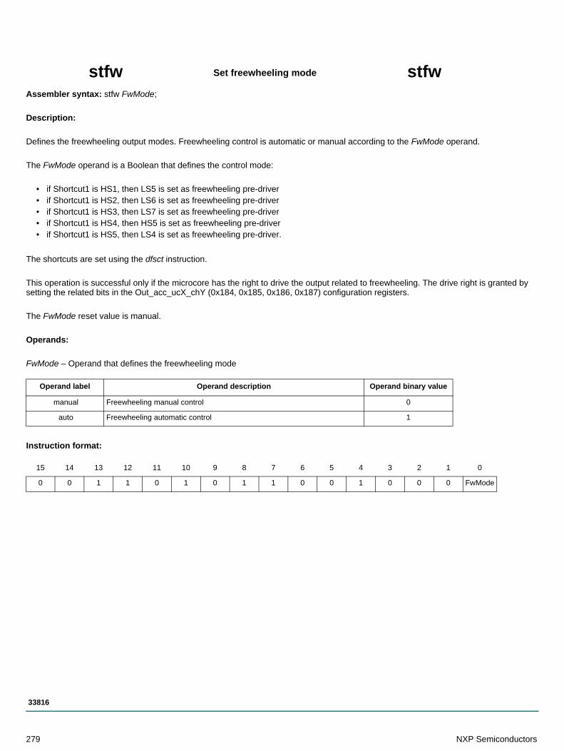
Assembler syntax: stfw FwMode;
Description:
Defines the freewheeling output modes. Freewheeling control is automatic or manual according to the FwMode operand.
The FwMode operand is a Boolean that defines the control mode:
• if Shortcut1 is HS1, then LS5 is set as freewheeling pre-driver• if Shortcut1 is HS2, then LS6 is set as freewheeling pre-driver• if Shortcut1 is HS3, then LS7 is set as freewheeling pre-driver• if Shortcut1 is HS4, then HS5 is set as freewheeling pre-driver• if Shortcut1 is HS5, then LS4 is set as freewheeling pre-driver.
The shortcuts are set using the dfsct instruction.
This operation is successful only if the microcore has the right to drive the output related to freewheeling. The drive right is granted by setting the related bits in the Out_acc_ucX_chY (0x184, 0x185, 0x186, 0x187) configuration registers.
The FwMode reset value is manual.
Operands:
FwMode – Operand that defines the freewheeling mode
Instruction format:
stfw Set freewheeling mode stfw
Operand label Operand description Operand binary value
manual Freewheeling manual control 0
auto Freewheeling automatic control 1
15 14 13 12 11 10 9 8 7 6 5 4 3 2 1 0
0 0 1 1 0 1 0 1 1 0 0 1 0 0 0 FwMode
279 NXP Semiconductors
33816

Assembler syntax: stgn Gain OpAmp;
Description:
Sets the gain of an operational amplifier with the Gain operand used to measure the current flowing through the actuator sense resistor. The operational amplifier is selected according to the OpAmp operand.
The operation is successful only if the microcore has the right to access the related current measurement block. The access right is granted by setting the related bits in the Cur_block_access_1 register (0x188) and Cur_block_access_2 Register (0x189).
The Gain reset value is gain 5.8.
Operands:
Gain – Operand that defines the current measure operational amplifier gain
OpAmp – Operand that defines the current measure operational amplifier gain to be set
Instruction format:
stgn Set current measure operational amplifier gain stgn
Operand label Operand description Operand binary value
gain5.8 Operational amplifier gain set to 5.8 00
gain8.7 Operational amplifier gain set to 8.7 01
gain12.6 Operational amplifier gain set to 12.6 10
gain19.3 Operational amplifier gain set to 19.3 11
Operand label Operand description Operand binary value
sssc Current measure operational amplifier of the same microcore same channel 00
ossc Current measure operational amplifier of the other microcore same channel 01
ssoc Current measure operational amplifier of the same microcore other channel 10
osoc Current measure operational amplifier of the other microcore other channel 11
15 14 13 12 11 10 9 8 7 6 5 4 3 2 1 0
0 0 1 1 0 1 0 1 0 0 1 1 Gain OpAmp
NXP Semiconductors 280
33816

Assembler syntax: stirq Logic;
Description:
Set the IRQB output pin
The Logic reset value is high.
Operands:
Logic – Operand that defines the logic level of the IRQB pin
Instruction format:
stirq Set IRQB pin stirq
Operand label Operand description Operand binary value
low Low level 0
high High level 1
15 14 13 12 11 10 9 8 7 6 5 4 3 2 1 0
0 0 1 1 0 1 0 1 1 0 0 1 0 0 1 Logic
281 NXP Semiconductors
33816

Assembler syntax: sto OutSel Out;
Description:
Sets the state with the Out operand for the selected output according to the OutSel operand.
The operation is successful only if the microcore has the right to drive the related outputs. The drive right is granted by setting the related bits in the Out_acc_ucX_chY (0x184, 0x185, 0x186, 0x187) configuration registers.
Operands:
OutSel – Operand that defines the handled output
Out – Operand that set output state
Instruction format:
sto Set single pre-driver output sto
Operand label Operand description Operand binary value
hs1 High-side pre-driver 1 0000
hs2 High-side pre-driver 2 0001
hs3 High-side pre-driver 3 0010
hs4 High-side pre-driver 4 0011
hs5 High-side pre-driver 5 0100
ls1 Low-side pre-driver 1 0101
ls2 Low-side pre-driver 2 0110
ls3 Low-side pre-driver 3 0111
ls4 Low-side pre-driver 4 1000
ls5 Low-side pre-driver 5 1001
ls6 Low-side pre-driver 6 1010
ls7 Low-side pre-driver 7 1011
undef Undefined 1100
Operand label Operand description Operand binary value
keep No changes, maintains the previous setting 00
off Output disabled 01
on Output enabled 10
toggle Reverse the previous setting 11
15 14 13 12 11 10 9 8 7 6 5 4 3 2 1 0
0 0 1 1 0 1 0 0 1 0 OutSel Out
NXP Semiconductors 282
33816

Assembler syntax: stoc Ctrl DacTraget;
Description:
Enables or disables the offset compensation with the operand Ctrl on the current measurement block specified according to the DacTarget operand.
The operation is successful only if the microcore has the right to access the related current measurement block. The access right is granted by setting the related bits in the Cur_block_access_1 register (0x188) and Cur_block_access_2 Register (0x189).
The Ctrl reset value is off for all current measurement blocks.
Operands:
Ctrl – Operands that set offset compensation state
DacTarget – Operand that defines the current measurement block
Instruction format:
stoc Set offset compensation stoc
Operand label Operand description Operand binary value
off Disable the offset compensation 0
on Enable the offset compensation 1
Operand label Operand description Operand binary value
sssc DAC of the same microcore same channel 00
ossc DAC of the other microcore same channel 01
ssoc DAC of the same microcore other channel 10
osoc DAC of the other microcore other channel 11
15 14 13 12 11 10 9 8 7 6 5 4 3 2 1 0
0 0 1 1 0 1 0 1 0 1 0 1 0 Ctrl DacTarget
283 NXP Semiconductors
33816

Assembler syntax: store op1 Dram Ofs;
Description:
Copies the content of the op1 source register in a Data RAM line defined by the 6-bit Data RAM address Dram.
The operand Dram can be identified with a univocal label. The compiler automatically substitutes the ‘define’ label (if used) with the suitable Data RAM address.
The Data RAM address is accessed according to the Boolean operand Ofs using the:
• Immediate addressing mode (IM).• Indexed addressing mode (XM). In that case,• the address base is added to the address Dram. The address base is set using the stab instructions.
Operands:
op1 – One of the register listed in the operand subset UcReg
Dram– Operand that defines the 6-bit DRAM address
Ofs– Operands that set data RAM addressing mode
Instruction format:
store Store register data in Data RAM store
Operand label Operand description Operand binary value
_ofs Data RAM immediate addressing mode (IM) 0
ofs Data RAM indexed addressing mode (XM) 1
15 14 13 12 11 10 9 8 7 6 5 4 3 2 1 0
1 0 Ofs op1 Dram 0 1
NXP Semiconductors 284
33816

Assembler syntax: stos Out1 Out2 Out3;
Description:
Sets the state of three outputs Out1, Out2 and Out3 previously defined as shortcuts with the dfsct instruction.
The operation is successful only if the microcore has the right to drive the related outputs. The drive right is granted by setting the related bits in the Out_acc_ucX_chY (0x184, 0x185, 0x186, 0x187) configuration registers.
Operands:
Out1, Out2, and Out3 – Operands that set output state
Instruction format:
stos Set pre-driver output shortcuts stos
Operand label Operand description Operand binary value
keep No changes, maintains the previous setting 00
off Output disabled 01
on Output enabled 10
toggle Reverse the previous setting 11
15 14 13 12 11 10 9 8 7 6 5 4 3 2 1 0
0 0 1 1 0 1 0 0 0 1 Out1 Out2 Out3
285 NXP Semiconductors
33816

Assembler syntax: stslew SlMode;
Description:
Defines the outputs slew rate mode with the Boolean SlMode.
The operation is successful only if the microcore has the right to drive the related outputs. The drive right is granted by setting the related bits in the Out_acc_ucX_chY (0x184, 0x185, 0x186, 0x187) configuration registers.
The SlMode reset value is normal.
When switching the slew-rate from slow to fast, the new slew-rate is valid after typically 1ck cycle (166 ns considering fck = 6.0 MHz).
When switching from fast to slow, it takes typically four ck cycles (666 ns considering fck = 6.0 MHz) until the new slew-rate is effective.
Operands:
SlMode – Operands that set outputs slew rate mode
Instruction format:
stslew Set pre-driver output slew rate mode stslew
Operand label Operand description Operand binary value
normal The outputs slew rate is set by an SPI register 0
fast The outputs slew rate is the highest one 1
15 14 13 12 11 10 9 8 7 6 5 4 3 2 1 0
0 0 1 1 0 1 0 1 1 0 0 1 0 1 1SlMod
e
NXP Semiconductors 286
33816

Assembler syntax: stsrb Logic SrbSel;
Description:
Sets individually the logic level value with the Logic operand of each selected bit SrbSel of the status register.
Operands:
Logic – Operand that defines the logic level value
SrbSel – Operand that defines the status register bit to be selected
Instruction format:
stsrb Set status register bit stsrb
Operand label Operand description Operand binary value
low Low level 0
high High level 1
Operand label Operand description Operand binary value
b0 Status register bit 0 (LSB) 0000
b1 Status register bit 1 0001
b2 Status register bit 2 0010
b3 Status register bit 3 0011
b4 Status register bit 4 0100
b5 Status register bit 5 0101
b6 Status register bit 6 0110
b7 Status register bit 7 0111
b8 Status register bit 8 1000
b9 Status register bit 9 1001
b10 Status register bit 10 1010
b11 Status register bit 11 1011
b12 Status register bit 12 1100
b13 Status register bit 13 1101
b14 Status register bit 14 1110
b15 Status register bit 15 (MSB) 1111
15 14 13 12 11 10 9 8 7 6 5 4 3 2 1 0
0 0 1 1 0 1 1 1 0 0 0 Logic SrbSel
287 NXP Semiconductors
33816

Operation: (Source1) - (Source2) => (Destination)
Assembler syntax: sub op1 op2 res;
Description:
Subtracts the value contained in the op1 register to the value contained in op2 register and places the result in the res register.
Operands:
op1 – One of the register listed in the operand subset AluReg
op2 – One of the register listed in the operand subset AluReg
res – One of the register listed in the operand subset AluReg
Condition register:
RZ - Addition or subtraction result is zero
RS - Addition or subtraction result is negative
UU - Unsigned underflow
UO - Unsigned overflow
SU - Signed underflow
SO - Signed overflow
Instruction format:
sub Two ALU registers subtraction to ALU register sub
15 14 13 12 11 10 9 8 7 6 5 4 3 2 1 0
0 0 1 0 1 0 res 1 op2 op1
NXP Semiconductors 288
33816

Operation: (Source) - Immediate value => (Destination)
Assembler syntax: subi op1 Imm res;
Description:
Subtracts the value contained in the Imm register to the value contained in the op1 register and places the result in the res register.
Operands:
op1 – One of the register listed in the operand subset AluReg
Imm –The Imm 4-bit immediate data register
res – One of the register listed in the operand subset AluReg
Condition register:
RZ - Addition or subtraction result is zero
RS - Addition or subtraction result is negative
UU - Unsigned underflow
UO - Unsigned overflow
SU - Signed underflow
SO - Signed overflow
Instruction format:
subi ALU register subtraction with immediate value to ALU register subi
15 14 13 12 11 10 9 8 7 6 5 4 3 2 1 0
0 0 0 1 1 1 res Imm op1
289 NXP Semiconductors
33816

Operation: (Source)[0:7] < => (Source)[8:15]
Assembler syntax: swap op1;
Description:
Swaps the high byte and the low byte of the register op1.
Operands:
op1 – One of the register listed in the operand subset AluReg
Instruction format:
swap Swap bytes inside ALU register swap
15 14 13 12 11 10 9 8 7 6 5 4 3 2 1 0
0 0 1 1 0 1 0 1 0 1 1 0 0 op1
NXP Semiconductors 290
33816

Assembler syntax: toc2 op1;
Description:
Converts the integer value contained in op1 register to two’s complement format.
If the conversion bit CS in the arithmetic condition register arith_reg is zero, the toc2 instruction set the operand register MSB to zero.
If the conversion bit is one, then it returns the 2's complement of the operand (bits[14:0] only) register op1 and set the MSB to one.Operands:
op1 – One of the register listed in the operand subset AluReg
Instruction format:
toc2 Integer to two’s complement conversion in ALU register toc2
15 14 13 12 11 10 9 8 7 6 5 4 3 2 1 0
0 0 1 1 0 1 1 1 0 0 1 1 0 op1
291 NXP Semiconductors
33816

Assembler syntax: toint op1 Rst;
Description:
Convert the two’s complement value contained in op1 register to integer format.
The toint instruction retains the original value in the operand register op1 when its MSB bit is zero.
If the MSB is 1, then it returns the 2's complement of the operand register (op1[14:0]).
The toint instruction also saves the MSB of the operand op1 in the conversion bit CS of the arithmetic condition register arith_reg.
The MSB of the operand is either XORed with the existing conversion bit CS of the ALU condition register (if the instruction is called with the _rst parameter) or replaces it (if the instruction is called with the rst parameter).
Operands:
op1 – One of the register listed in the operand subset AluReg
Rst – Operand that defines if the conversion bit CS of the ALU condition register is reset
Condition register:
CS - Last conversion sign
Instruction format:
toint two’s complement to integer conversion in ALU register toint
Operand label Operand description Operand binary value
_rst The existing conversion bit CS is XORed with the op1 MSB 0
rst The existing conversion bit CS is set according to the op1 MSB 1
15 14 13 12 11 10 9 8 7 6 5 4 3 2 1 0
0 0 1 1 0 1 1 1 0 0 1 0 Rst op1
NXP Semiconductors 292
33816

Assembler syntax: wait WaitMask ;
Description:
Stops the program counter (uPC) incrementing and waits until at least one of the enabled wait conditions is satisfied. When one of the conditions is satisfied, the program counter is moved to the corresponding destination.
The possible wait conditions, along with the corresponding destinations, are stored in the wait table by means of the cwer and cwef instructions.
The active wait table rows are enabled according to the WaitMask 5-bit operand.
Operands:
WaitMask – Operand that defines the active wait table rows
wait Wait until condition satisfied wait
Operand label Operand description Operand binary value
always No wait table row enabled. Infinite loop 00000
row1 Wait table row 1 enabled 00001
row2 Wait table row 2 enabled 00010
row12 Wait table row 1,2 enabled 00011
row3 Wait table row 3 enabled 00100
row13 Wait table row 1,3 enabled 00101
row23 Wait table row 2,3 enabled 00110
row123 Wait table row 1,2,3 enabled 00111
row4 Wait table row 4 enabled 01000
row14 Wait table row 1,4 enabled 01001
row24 Wait table row 2,4 enabled 01010
row124 Wait table row 1,2,4 enabled 01011
row34 Wait table row 3,4 enabled 01100
row134 Wait table row 1,3,4 enabled 01101
row234 Wait table row 2,3,4 enabled 01110
row1234 Wait table row 1,2,3,4 enabled 01111
row5 Wait table row 5 enabled 10000
row15 Wait table row 1,5 enabled 10001
row25 Wait table row 2,5 enabled 10010
row125 Wait table row 1,2,5 enabled 10011
row35 Wait table row 3,5 enabled 10100
row135 Wait table row 1,3,5 enabled 10101
row235 Wait table row 2,3,5 enabled 10110
row1235 Wait table row 1,2,3,5 enabled 10111
row45 Wait table row 4,5 enabled 11000
row145 Wait table row 1,4,5 enabled 11001
293 NXP Semiconductors
33816

Instruction format:
row245 Wait table row 2,4,5 enabled 11010
row1245 Wait table row 1,2,4,5 enabled 11011
row345 Wait table row 3,4,5 enabled 11100
row1345 Wait table row 1,3,4,5 enabled 11101
row2345 Wait table row 2,3,4,5 enabled 11110
row12345 Wait table row 1,2,3,4,5 enabled 11111
15 14 13 12 11 10 9 8 7 6 5 4 3 2 1 0
0 0 1 1 0 1 0 1 0 0 0 WaitMask
Operand label Operand description Operand binary value
NXP Semiconductors 294
33816

Assembler syntax: wrspi;
Description:
Requests an SPI backdoor write.
The address must previously be defined in the SPI address register spi_add.
The data must previously be defined in the SPI address register spi_data register.
The wrspi instruction requires 2 ck cycles to complete operation. The SPI address register and SPI data register must not be changed on the following instruction, otherwise the operation fails and the written data is dummy.
Instruction format:
wrspi SPI write request wrspi
15 14 13 12 11 10 9 8 7 6 5 4 3 2 1 0
0 0 1 1 0 1 0 1 0 1 0 0 0 0 0 1
295 NXP Semiconductors
33816

Operation: (Source) + Immediate register => (Source)
Assembler syntax: xor op1;
Description:
Applies the XOR-mask contained into the Ir register to the value contained in the op1 register and places the result in the op1 register. The initial data stored in the op1 register is loss.
Operands:
op1 – One of the register listed in the operand subset AluReg
Ir –The ALU immediate register
Condition register:
MM - Mask result is 0x0000
MN - Mask result is 0xFFFF
Instruction format:
xorXOR-mask on ALU register with the immediate register to ALU
register xor
15 14 13 12 11 10 9 8 7 6 5 4 3 2 1 0
0 0 1 0 1 1 1 0 1 1 0 1 0 op1
NXP Semiconductors 296
33816

11 Packaging
11.1 Package mechanical dimensions
Package dimensions are provided in package drawings. To find the most current package outline drawing, go to www.NXP.com and perform a keyword search for the drawing’s document number.
Table 231. Packaging information
Package Suffix Package outline drawing number
64-Pin LQFP Exposed Pad AE 98ASA00237D
297 NXP Semiconductors
33816

NXP Semiconductors 298
33816

299 NXP Semiconductors
33816

NXP Semiconductors 300
33816

12 Revision history
Revision Date Description of changes
1.0 7/2012 • Initial release
2.0 11/2012• Wording and part definitions changes were made. • No electrical content was altered.
3.01/2014
• Corrected errors, typos, and formatting• Added HSX leakage current when pre-driver on (biasing switched off) and S_HSX leakage current delta
between pre-drivers off and on parameters• Changed min for VB_HSX_VCCP__TH_R and VB_HSX_VCCP__TH_F• Added missing sentence for Cipher_unit block
1/2014 • Updated Data Sheet title
4.0 4/2014• Redefined the minimum for tCSBF_SCLKR and tSCLKF_CSBR in Table 75.• Removed associated table and graphic for tCSBF_SCLKR and tSCLKF_CSBR.
5.0 9/2014
• Updated Note (9)
• Updated Table 4 (added min. and max. value for RJA) • Updated Figure 7 (added DGND to ground symbol)• Added Table 11 for VCC5 Slew Rate• Updated Figure 10 (added PGND to the ground symbol)• Updated Table 16 (changed cksys_drven to 1 for the last two cases)• Updated Table 22 (added total DAC error)• Updated Table 38 (changed cksys_drven to 1 for the last case)• Updated (63) (changed 330 nF to 330 pF)• Updated Section 6.15.2 Clock_manager block on page 88• Updated timing in Table 163• Updated reset values in Table 192, Table 193, and Table 194• Updated operand description for Sh1 and Sh2 on page 247• Updated mask values for steoa instruction
6.0 4/2015
• Updated Table 3 (replaced high-side with low-side)• Updated Table 38 (set Drven to 1)• Table 39, clarified the maximum PWM frequency• Table 93, changed flag 11 from OA1 to OA2• Replaced IRQ by IRQB• Updated reset value in Table 152 for boost feedback filter• Updated hs1 and hs2 ls act disable description• Updated dac_4neg from 8 bits to 4 bits in Table 181• Updated Table 204 (dead time from 4 bits to 5 bits)• Corrected typo error in Table 221 (decimal replaced with hexadecimal)• Updated operand label in Bias instruction
7.0 8/2016• Updated to NXP document form and style• Added 69 V parameter to VCP_SRC in Table 37• Added tSPI_RESETB_T0 and tSPI_RESETB parameters to Table 75
8.0 4/2018
• Updated conditions for parameter IVBOOST_QUIESC in Table 6• Deleted Figure 24• Updated text in Section 6.15.5.15 Mode B• Updated text in Section 6.15.5.15.1 Spi_error block
301 NXP Semiconductors
33816

Information in this document is provided solely to enable system and software implementers to use NXP products.
There are no expressed or implied copyright licenses granted hereunder to design or fabricate any integrated circuits
based on the information in this document. NXP reserves the right to make changes without further notice to any
products herein.
NXP makes no warranty, representation, or guarantee regarding the suitability of its products for any particular
purpose, nor does NXP assume any liability arising out of the application or use of any product or circuit, and
specifically disclaims any and all liability, including without limitation, consequential or incidental damages. "Typical"
parameters that may be provided in NXP data sheets and/or specifications can and do vary in different applications,
and actual performance may vary over time. All operating parameters, including "typicals," must be validated for each
customer application by the customer's technical experts. NXP does not convey any license under its patent rights nor
the rights of others. NXP sells products pursuant to standard terms and conditions of sale, which can be found at the
following address:
http://www.nxp.com/terms-of-use.html.
How to Reach Us:
Home Page: NXP.com
Web Support: http://www.nxp.com/support
NXP, the NXP logo, Freescale, the Freescale logo, and SMARTMOS are trademarks of NXP B.V. All other product or
service names are the property of their respective owners. All rights reserved.
© NXP B.V. 2018
Document Number: MC33816Rev. 8.0
4/2018