mc33094, ignition control control designed for autom ... 14 s current sense spark coil current...
TRANSCRIPT
Document Number: MC33094Rev. 1.0, 10/2006
Freescale Semiconductor Advance Information
Ignition ControlDesigned for automotive ignition applications in 12 V systems, the
33094 provides outstanding control of the ignition coil when used with an appropriate Motorola Power Darlington Transistor. Engine control systems utilizing these devices for ignition coil control exhibit exceptional fuel efficiency and low exhaust emissions. The device is designed to be controlled from a single–ended Hall Sensor input. The circuit is built using high–density Integrated–Injection Logic (IIL) processing incorporating high current–gain PNP and NPN transistors.
The 33094 is packaged in an economical surface mount package and specified over an ambient temperature of –40°C to 125°C with a maximum junction temperature of 150°C.
Features• External Capacitors Program the Device’s Timing Characteristics• Overvoltage Shutdown Protection• Auto Start–Up Capability After Overvoltage Condition Ceases• Allows for Push Start–Up in Automotive Applications• Ignition Coil Current Limiting• Ignition Coil Voltage Limiting• Band Gap Reference for Enhanced Stability Over Temperature• Negative Edge Filter for Hall Sensor Input Transient Protection• Hall Sensor Inputs for RPM and Position Sensing• Pb-Free Packaging Designated by Suffix Code EG
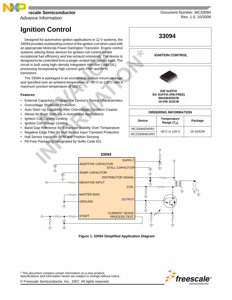
Figure 1. 33094 Simplified Application Diagram
IGNITION CONTROL
DW SUFFIXEG SUFFIX (PB-FREE)
98ASB42567B16-PIN SOICW
33094
ORDERING INFORMATION
Device Temperature Range (TA) Package
MC33094DW/R2-40°C to 125°C 16 SOICW
MCZ33094EG/R2
33094
MASTER BIAS
ADAPTIVE CAPACITOR
RAMP CAPACITOR
GROUND
NEGATIVE INPUT
START
STALL CAPACITOR
CURRENT SENSEPROCESS TEST
OUTPUT
COIL
DISTRIBUTOR SIGNAL
SUPPLY
* This document contains certain information on a new product. Specifications and information herein are subject to change without notice.
© Freescale Semiconductor, Inc., 2007. All rights reserved.
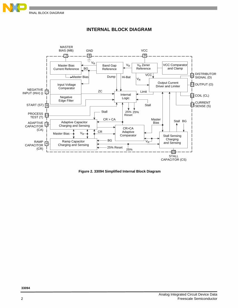
INTERNAL BLOCK DIAGRAM
INTERNAL BLOCK DIAGRAM
Figure 2. 33094 Simplified Internal Block Diagram
BG
VR
ZC
Stall
Stall
Stall
NegativeEdge Filter
Input VoltageComparator
Master Bias
Master BiasCurrent Reference
Band GapReference
InternalLogic
Adaptive CapacitorCharging and Sensing
Master Bias VR
Ramp CapacitorCharging and Sensing
BG
25% Reset25%
VR
CR
CR > CA
Dump Hi-Bat
VR
VR
VR ZenerReference
VCC Comparatorand Clamp
Output CurrentDriver and Limiter
Limit
25%Reset
25%
CR>CAAdaptive
Comparator
MasterBias
Stall SensingCharging
and Sensing
BG
VCC
GNDMASTER
BIAS (MB) VCC
DISTRIBUTORSIGNAL (D)
OUTPUT (O)
COIL (CL)
CURRENTSENSE (S)
NEGATIVEINPUT (INV(-))
START (ST)
PROCESSTEST (T)
ADAPTIVECAPACITOR
RAMPCAPACITOR
2
3
4
6
7
8
9
10
11
12
13
14
15STALL
CAPACITOR (CS)
(CA)
(CR)
Analog Integrated Circuit Device Data 2 Freescale Semiconductor
33094
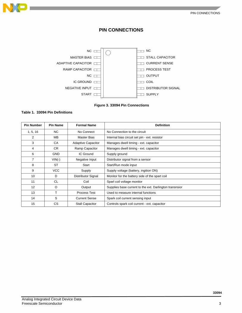
PIN CONNECTIONS
PIN CONNECTIONS
Figure 3. 33094 Pin Connections Table 1. 33094 Pin Definitions
Pin Number Pin Name Formal Name Definition
1, 5, 16 NC No Connect No Connection to the circuit
2 MB Master Bias Internal bias circuit set pin - ext. resistor
3 CA Adaptive Capacitor Manages dwell timing - ext. capacitor
4 CR Ramp Capacitor Manages dwell timing - ext. capacitor
6 GND IC Ground Supply ground
7 VIN(-) Negative Input Distributor signal from a sensor
8 ST Start Start/Run mode input
9 VCC Supply Supply voltage (battery, ingition ON)
10 D Distributor Signal Monitor for the battery side of the spart coil
11 CL Coil Sparl coil voltage monitor
12 O Output Supplies base current to the ext. Darlington transnsior
13 T Process Test Used to measure internal functions
14 S Current Sense Spark coil current sensing input
15 CS Stall Capacitor Controls spark coil current - ext. capacitor
NC
STALL CAPACITOR
CURRENT SENSE
PROCESS TEST
OUTPUT
COIL
DISTRIBUTOR SIGNAL
SUPPLY
NC
MASTER BIAS
ADAPTIVE CAPACITOR
RAMP CAPACITOR
NC
IC GROUND
NEGATIVE INPUT
START
Analog Integrated Circuit Device Data Freescale Semiconductor 3
33094
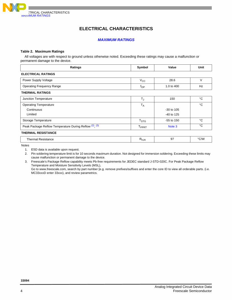
ELECTRICAL CHARACTERISTICSMAXIMUM RATINGS
ELECTRICAL CHARACTERISTICS
MAXIMUM RATINGS
Table 2. Maximum Ratings
All voltages are with respect to ground unless otherwise noted. Exceeding these ratings may cause a malfunction or permanent damage to the device.
Ratings Symbol Value Unit
ELECTRICAL RATINGS
Power Supply Voltage VCC 28.6 V
Operating Frequency Range fOP 1.0 to 400 Hz
THERMAL RATINGS
Junction Temperature TJ 150 °C
Operating TemperatureContinuousLimited
TA
-30 to 105-40 to 125
°C
Storage Temperature TSTG -55 to 150 °C
Peak Package Reflow Temperature During Reflow (2), (3) TPPRT Note 3 °C
THERMAL RESISTANCE
Thermal Resistance RθJA 97 °C/W
Notes1. ESD data is available upon request.2. Pin soldering temperature limit is for 10 seconds maximum duration. Not designed for immersion soldering. Exceeding these limits may
cause malfunction or permanent damage to the device.3. Freescale’s Package Reflow capability meets Pb-free requirements for JEDEC standard J-STD-020C. For Peak Package Reflow
Temperature and Moisture Sensitivity Levels (MSL), Go to www.freescale.com, search by part number [e.g. remove prefixes/suffixes and enter the core ID to view all orderable parts. (i.e. MC33xxxD enter 33xxx), and review parametrics.
Analog Integrated Circuit Device Data 4 Freescale Semiconductor
33094
ELECTRICAL CHARACTERISTICSSTATIC ELECTRICAL CHARACTERISTICS
STATIC ELECTRICAL CHARACTERISTICS
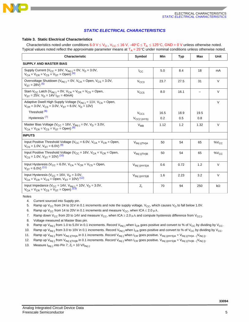
Table 3. Static Electrical Characteristics Characteristics noted under conditions 6.0 V ≤ VD = VCC ≤ 16 V, - 40°C ≤ TA ≤ 125°C, GND = 0 V unless otherwise noted.
Typical values noted reflect the approximate parameter means at TA = 25°C under nominal conditions unless otherwise noted.
Characteristic Symbol Min Typ Max Unit
SUPPLY AND MASTER BIAS
Supply Current (VCC = 16V, VIN(-) = 0V, VD = 3.0V, VCA = VCR = VCS = VST = Open) (4)
ICC 5.0 8.4 18 mA
Overvoltage Shutdown (VIN(-) = 0V, VCA = Open, VCS = 3.0V, VST = 28V) (5)
VCC3 23.7 27.5 31 V
Start-VCC Latch (VIN(-) = 0V, VCA = VCR = VCS = Open, VST = 25V, VD = 14V IST = 40mA)
VCC5 8.0 16.1 – V
Adaptive Dwell High Supply Voltage (VIN(-) = 11V, VCA = Open, VCR = 3.0V, VCS = 3.0V, VST = 6.0V, VD = 13V)
Threshold (6)
Hysteresis (7)VCC1
VCC2 (HYS)
16.50.2
18.90.5
19.50.8
V
Master Bias Voltage (VCC = 16V, VIN(-) = 0V, VD = 3.0V, VCA = VCR = VCS = VST = Open) (8)
VMB 1.12 1.2 1.32 V
INPUTS
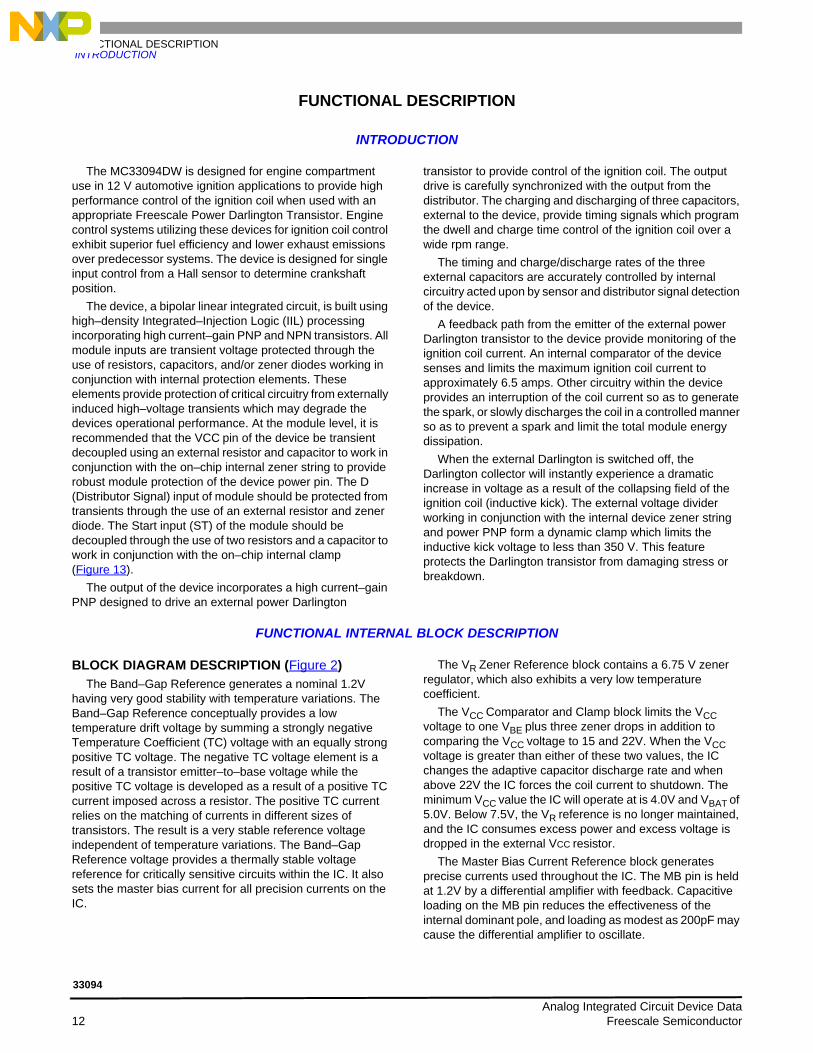
Input Positive Threshold Voltage (VCC = 6.0V, VCA = VCR = Open, VCS = 1.0V, VST = 6.0V) (9)
VIN(-)(TH)A 50 54 65 %VCC
Input Positive Threshold Voltage (VCC = 16V, VCA = VCR = Open, VCS = 1.0V, VST = 10V) (10)
VIN(-)(TH)B 50 54 65 %VCC
Input Hysteresis (VCC = 6.0V, VCA = VCR = VCS = Open, VST = 6.0V) (11)
VIN(-)(HYS)A 0.6 0.72 1.2 V
Input Hysteresis (VCC = 16V, VD = 3.0V, VCA = VCR = VCS = Open, VST = 10V) (12)
VIN(-)(HYS)B 1.6 2.23 3.2 V
Input Impedance (VCC = 14V, VIN(-) = 10V, VD = 3.0V, VCA = VCR = VCS = VST = Open) (13)
ZI 70 94 250 kΩ
Notes4. Current sourced into Supply pin.5. Ramp up VCC from 24 to 31V in 0.1 increments and note the supply voltage, VCC, which causes VO to fall below 1.0V.6. Ramp up VCC from 14 to 20V in 0.1 increments and measure VCC, when ICA ≤ 2.0 µΑ.7. Ramp down VCC from 20 to 14V and measure VCC, when ICA ≥ 2.0 µΑ and compute hysteresis difference from VCC1.8. Voltage measured at Master Bias pin.9. Ramp up VIN(-) from 1.0 to 5.0V in 0.1 increments. Record VIN(-) when ICR goes positive and convert to % of VCC by dividing by VCC.
10. Ramp up VIN(-) from 3.0 to 10V in 0.1 increments. Record VIN(-) when ICR goes positive and convert to % of VCC by dividing by VCC.11. Ramp up VIN(-) from VIN(-)(TH)A in 0.1 increments. Record VIN(-) when ICR goes positive. VIN(-)(HYS)A = VIN(-)(TH)A - (VIN(-)).12. Ramp up VIN(-) from VIN(-)(TH)B in 0.1 increments. Record VIN(-) when ICR goes positive. VIN(-)(HYS)B = VIN(-)(TH)B - (VIN(-)).13. Measure IIN(-) into Pin 7; ZI = 10 V/IIN(-).
Analog Integrated Circuit Device Data Freescale Semiconductor 5
33094
ELECTRICAL CHARACTERISTICSSTATIC ELECTRICAL CHARACTERISTICS
OUTPUT AND DWELL
Output Current (VIN(-) = 0V, VCA = VCR = Open, VCS = 3.0V, VST = 10V, VO = 2.1V) (14)
Normal Condition (VCC = 14V, VD = 6.0V)
High Voltage Condition (VCC = 14V, VD = 22V)IO1
IO2
4040
5252
6565
mA
Output Leakage Current (VCC = 14V, VIN(-) = 10V, VCA = VCR = VCS = Open, VST = 10V, VS = 0V, VD = 18V, VO = 0V) (15)
IO3 1.0 -1.33 100 µA
Output Clamp Voltage (VCC = 14V, VIN(-) = 10V, VCA = VCR = VCS = Open, VST = 10V, VD = 14V, VO = 0V, VCL = 20V, ICL = 10mA) (16)
VCL 13.7 14.52 15.58 V
Output Clamp Dynamic Impedance (VCC = 14V, VIN(-) = 10V, VCA = VCR = VCS = Open, VST = 10V, VD = 14V, VO = 0V, ICL = 12mA, ∆ICL = 2.0mA) (17)
ZCL 10 37 75 Ω
Dwell (18)
Normal Condition: D1 = (ICA2/ICA1) x CR Data from ICA2, ICA1, and CR characteristics
High Voltage Condition: D2 = (ICA3/ICA1) x CR Data from ICA3, ICA1, and CR characteristics
D1
D2
14.5
4.1
17.6
5.3
20.5
5.9
%
Adaptive Dwell Logic, Ramp Threshold (VCC = 14V, VIN(-) = 10V, VCA = VCS = Open, VST = 0V, VS = 0V, VD = 10V) (14)
VCRO -60 0 60 mV
Soft Shutdown Voltage (VCC = 6.0V, VIN(-) = 10V, VCA = VCR = VCS = Open, VST = 0V) Measure VS
VSS 0 1.48 16.7 mV
Notes14. Capability measured by forcing the Output to 2.0V with the Current Sense pin (S) open while measuring the Output current to ground.15. Measured by clamping the output voltage with the S pin to ground, then increasing the VD from 6.0 to 18V and measuring output leakage
current to ground.16. Output Clamp voltage with reference to ground while forcing 10mA into the Coil pin (CL).17. Output Clamp impedance measured with ICL = 11 ±1.0mA into the Coil pin (CL) and noting the corresponding Output Clamp Voltage
change (ZCL = ∆VCL/∆ICL).18. Dwell is defined as Run Mode Down Current divided by the Run Mode Up Current times the Ramp Control Current Ratio and is
calculated from other measured characteristics as defined above.19. Set the VCR (ramp Capacitor) voltage to 1.5V; Ramp VCR voltage from 1.8 to 2.2V in 0.02V increments and note the Ramp voltage (VCR)
which causes the Output voltage to go > 1.0V; VCRO = 2.0V - VCR.
Table 3. Static Electrical Characteristics (continued)Characteristics noted under conditions 6.0 V ≤ VD = VCC ≤ 16 V, - 40°C ≤ TA ≤ 125°C, GND = 0 V unless otherwise noted.
Typical values noted reflect the approximate parameter means at TA = 25°C under nominal conditions unless otherwise noted.
Characteristic Symbol Min Typ Max Unit
Analog Integrated Circuit Device Data 6 Freescale Semiconductor
33094

ELECTRICAL CHARACTERISTICSSTATIC ELECTRICAL CHARACTERISTICS
ADAPTIVE CAPACITOR
Run Mode, Adaptive, Charge Current (VCC = 6.0V, VIN(-) = 5.0V, VCA = Open, VCR = 3.0V, VCS = 3.0V, VST = 6.0V) (20)
ICA1 -7.91 -6.53 -5.62 µA
Run Mode, Adaptive Capacitor, Discharge Current (VCA = Open, VCR = 3.0V, VCS = 3.0V, VST = 6.0V)
Normal Condition (VCC = 6.0V, VIN(-) = 10V)
High Voltage Condition (VCC = 22V, VIN(-) = 17V, VD = 13V)ICA2
ICA3
3.71.05
4.771.43
5.631.82
µA
Start Mode, Adaptive Capacitor Currents (VCA = VCR = VCS = Open, VST = 10V)
Charge Current (VCC = 5.0V, VIN(-) = 10V) (21)
Discharge Current (VCC = 6.0V, VIN(-) = 0V) (22)
ICA4
ICA5
-11267.6
-8789.4
-80109
µA
Start Mode, Adaptive Capacitor, Clamp Voltage (VCC = 6.0V, VCA = VCR = VCS = Open, VST = 10V)
High Clamp Voltage (VIN(-) = 10V)
Low clamp Voltage (VIN(-) = 0V) VCA1
VCA2
2.230.95
2.301.1
2,651.26
V
Adaptive Gain (VCC = 14V, VIN(-) = 11V, VST = 6.0V, VCA = Open, VCR = 3.0V, VCS = 3.0V, VD = 13V) (23)
AG 0.85 0.99 1.15 Times
STALL CAPACITOR
Start Mode, Stall Control, Charge Current (VCC = 5.0V, VIN(-) = 0V, VCA = VCR = Open, VCS = 1.0V, VST = 10V)
ICS1 -2.7 -2.33 -2.13 µA
Run Mode, Stalled, Stall Control, Discharge Current (VCC = 14V, VIN(-) = 0V, VCA = VCR = Open, VCS = 1.0V, VST = 0V)
ICS2 7.5 9.69 13.2 µA
Run Mode, Stall Control, Charge Current (VCC = 14V, VIN(-) = 10V, VCA = 2.0V, VCR = 3.0V, VCS = 1.0V, VST = 0V)
ICS3 -33.1 -27 -23.5 µA
Run Mode, Stall Control, Discharge Current (VCC = 14V, VIN(-) = 10V, VCA = 2.0V, VCR = Open, VCS = 1.0V, VST = 0V, VMB = 0V)
ICS4 0.76 1.02 1.26 µA
Stall Control Threshold Voltage (VCC = 14V, VIN(-) = 0V, VCA = VCR = Open, VST = 0V) (24)
VCS1 1.95 2.06 2.45 V
Stall Control Saturation Voltage (VCC = 14V, VIN(-) = 0V, VCA = VCR = VCS = Open, VST = 0V)
VCS2 20 35.3 165 mV
Notes20. Open VCR (Ramp Capacitor) initially then force VCR = 3.9V and measure ICA1.21. Start Mode Adaptive Control sourcing current.22. Start Mode Adaptive Control sink current.23. Measure ICA. Calculate: AG = ICR1/ICA.24. Ramp VCS (Stall Capacitor) from 1.5 to 2.5V in 20 mV steps. Record VCS when ICS goes negative.25. Set VST = 10V, VCS = 1.0V, Fail if output is on. Set VCS = 3.0V, Fail if output in off.
Table 3. Static Electrical Characteristics (continued)Characteristics noted under conditions 6.0 V ≤ VD = VCC ≤ 16 V, - 40°C ≤ TA ≤ 125°C, GND = 0 V unless otherwise noted.
Typical values noted reflect the approximate parameter means at TA = 25°C under nominal conditions unless otherwise noted.
Characteristic Symbol Min Typ Max Unit
Analog Integrated Circuit Device Data Freescale Semiconductor 7
33094
ELECTRICAL CHARACTERISTICSSTATIC ELECTRICAL CHARACTERISTICS
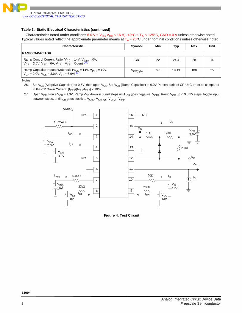
Figure 4. Test Circuit
RAMP CAPACITOR
Ramp Control Current Ratio (VCC = 14V, VIN(-) = 0V, VCR = 3.0V, VST = 0V, VCA = VCS = Open) (26)
CR 22 24.4 28 %
Ramp Capacitor Reset Hysteresis (VCC = 14V, VIN(-) = 10V, VCA = 2.0V, VCS = 3.0V, VST = 6.0V) (27)
VCR(hyh) 6.0 19.19 180 mV
Notes26. Set VCA (Adaptive Capacitor) to 0.5V, then open VCA. Set VCR (Ramp Capacitor) to 0.9V Percent ratio of CR UpCurrent as compared
to the CR Down Current; (ICR1/(ICR1-ICR2) x 100).27. Open VCR, Force VCR = 1.3V. Ramp VCR down in 30mV steps until ICR goes negative, VCR1. Ramp VCR up in 3.0mV steps, toggle input
between steps, until ICR goes positive, VCR2. VCR(hys)-VCR2 - Vcr1.
Table 3. Static Electrical Characteristics (continued)Characteristics noted under conditions 6.0 V ≤ VD = VCC ≤ 16 V, - 40°C ≤ TA ≤ 125°C, GND = 0 V unless otherwise noted.
Typical values noted reflect the approximate parameter means at TA = 25°C under nominal conditions unless otherwise noted.
Characteristic Symbol Min Typ Max Unit
1
2
3
4
5
6
7
8 9
10
11
12
13
14
15
16
VMB
NC NC
NC
15.25kΩ
VCA2.0V
VCR3.0V
VIN(-)10V
VST0V
VCS3.0V
VD13V
VCC13V
ICA
ICR
IIN(-)
IST
5.0kΩ
27kΩ
ICC
ID
250Ω
55Ω
10Ω 20Ω
200Ω
ICL
VCL
VO
ICS
VS
+
+
+
+ +
+
+
Analog Integrated Circuit Device Data 8 Freescale Semiconductor
33094
ELECTRICAL CHARACTERISTICSDYNAMIC ELECTRICAL CHARACTERISTICS
DYNAMIC ELECTRICAL CHARACTERISTICS
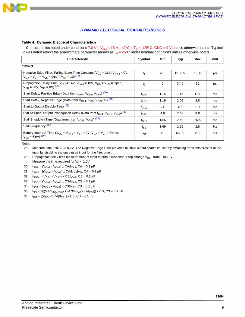
Table 4. Dynamic Electrical Characteristics
Characteristics noted under conditions 7.0 V ≤ VCC ≤ 18 V, - 40°C ≤ TA ≤ 125°C, GND = 0 V unless otherwise noted. Typical values noted reflect the approximate parameter means at TA = 25°C under nominal conditions unless otherwise noted.
Characteristic Symbol Min Typ Max Unit
TIMING
Negative Edge Filter, Falling Edge Time Constant (VCC = 16V, VIN(-) = 0V, VCA = VCR = VCS = Open, VST = 10V (28)
t1 400 613.65 1000 µs
Propagation Delay Time (VCC = 14V, VIN(-) = 10V, VCA = VCS = Open, VCR =3.0V, VST = 0V) (29)
t2 0 3.45 15 µs
Start Delay, Positive Edge (Data from ICA4, VCA1, VCA2) (30) tSDP 1.15 1.46 1.71 ms
Start Delay, Negative Edge (Data from VCA4, ICA5, VCA2, t1) (31) tSDN 1.19 2.06 2.8 ms
Start to Output Disable Time (32) tSOD 71 87 107 ms
Stall to Spark Output Propagation Delay (Data from ICS3, VCS1, VCS2) (33) tSSD 4.6 7.48 8.8 ms
Stall Shutdown Time (Data from ICS2, VCS1, VCS2) (34) tSST 13.6 20.9 26.5 ms
Stall Frequency (35) fSS 1.69 2.26 2.8 Hz
Battery Interrupt Time (VCC = VIN(-) = VST = 0V, VCA = VCR = Open, VCS = 6.0V) (36)
tBIT 25 66.65 200 ms
Notes28. Measure time until VO > 0.2V. The Negative Edge Filter prevents multiple output sparks caused by switching transients present at the
input by disabling the once used input for the filter time t.29. Propagation delay time measurement of input to output response; Step change VIN(-) from 0 to 10V.
Measure the time required for VO < 1.5V30. tSDP = (VCA1 - VCA2) x CA/ICA4; CA = 0.1 µF31. tSDN = [(VCA1 - VCA2) x CA/ICA5]+t1; CA = 0.1 µF32. tSOD = (VCA1 - VCA2) x CS/ICA1; CS = 0.1 µF33. tSSD = (VCA1 - VCA2) x CS/ICA3; CS = 0.1 µF34. tSST = (VCA1 - VCA2) x CS/ICA2; CS = 0.1 µF35. fSS = 1/[(5.4/VIN(-)(TH)) + (4.3/ICS4) + (2/ICS2)] x CS; CS = 0.1 µF36. tBIT = [(VCS - 0.7V)/ICS1] x CS; CS = 0.1 µF
Analog Integrated Circuit Device Data Freescale Semiconductor 9
33094
ELECTRICAL CHARACTERISTICSTIMING DIAGRAMS
TIMING DIAGRAMS
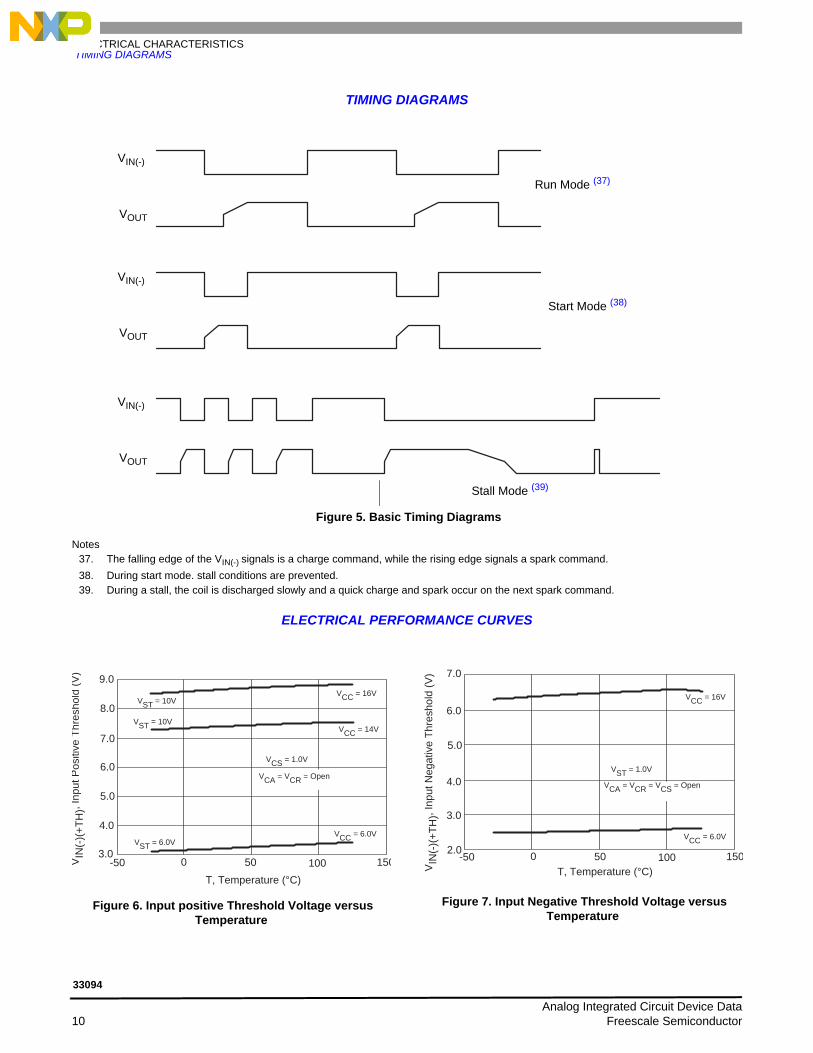
Figure 5. Basic Timing Diagrams
Notes37. The falling edge of the VIN(-) signals is a charge command, while the rising edge signals a spark command.38. During start mode. stall conditions are prevented.39. During a stall, the coil is discharged slowly and a quick charge and spark occur on the next spark command.
ELECTRICAL PERFORMANCE CURVES
Figure 6. Input positive Threshold Voltage versus Temperature
Figure 7. Input Negative Threshold Voltage versus Temperature
VIN(-)
VOUT
VIN(-)
VOUT
VIN(-)
VOUT
Run Mode (37)
Start Mode (38)
Stall Mode (39)
T, Temperature (°C)-50 0 50 100 150V
IN(-
)(+T
H),
Inpu
t Pos
itive
Thr
esho
ld (V
) 9.0
3.0
8.0
7.0
6.0
5.0
4.0
VST = 10V
VST = 10V
VST = 6.0V
VCC = 16V
VCC = 14V
VCC = 6.0V
VCS = 1.0V
VCA = VCR = Open
VIN
(-)(
+TH
), In
put N
egat
ive
Thre
shol
d (V
)
T, Temperature (°C)-50 0 50 100 150
3.0
7.0
6.0
5.0
4.0
2.0
VCC = 16V
VCC = 6.0V
VST = 1.0V
VCA = VCR = VCS = Open
Analog Integrated Circuit Device Data 10 Freescale Semiconductor
33094

ELECTRICAL CHARACTERISTICSELECTRICAL PERFORMANCE CURVES
Figure 8. Output Current Change versus Temperature
Figure 9. Input Impedance versus Temperature
Figure 10. Output Clamp Voltage versus Temperature
Figure 11. Output Clamp Dynamic Impedance versus Temperature
Figure 12. Supply Drain Current versus Temperature
∆IO
, Out
put C
urre
nt C
hang
e (%
)
T, Temperature (°C)-50 0 50 100 150
2.2
2.4
2.6
2.8
3.0
3.2
VO from 10 to 22V
T, Temperature (°C)-50 0 50 100 150
Z I, I
nput
Impe
denc
e (k
Ω)
40
60
80
100
120
140
160
VIN(-) = OpenVCC = 16VPin 6 = 10VZI = 10 V/IIN(-)
T, Temperature (°C)-50 0 50 100 150
VC
L, O
utpu
t Cla
mp
Vol
tage
(V)
14
14.2
14.4
14.6
14.8
15
15.2
VO - 0VICL = 10mA
T, Temperature (°C)-50 0 50 100 150
Z CL,
Out
put C
lam
p D
ynam
ic Im
pede
nce
(Ω)
25
30
35
40
45
50VO = 0VICL = 12mA∆ΙCL = 2.0mAZCL = ∆VCL/∆ΙCL
T, Temperature (°C)-50 0 50 100 150
I CC
, Sup
ply
Cur
rent
(mA
)
8.7
8.1
8.6
8.5
8.4
8.3
8.2
VIN(-) = 0VVCC = 6.0VVD = 3.0V
Analog Integrated Circuit Device Data Freescale Semiconductor 11
33094
FUNCTIONAL DESCRIPTIONINTRODUCTION
FUNCTIONAL DESCRIPTION
INTRODUCTION
The MC33094DW is designed for engine compartment use in 12 V automotive ignition applications to provide high performance control of the ignition coil when used with an appropriate Freescale Power Darlington Transistor. Engine control systems utilizing these devices for ignition coil control exhibit superior fuel efficiency and lower exhaust emissions over predecessor systems. The device is designed for single input control from a Hall sensor to determine crankshaft position.
The device, a bipolar linear integrated circuit, is built using high–density Integrated–Injection Logic (IIL) processing incorporating high current–gain PNP and NPN transistors. All module inputs are transient voltage protected through the use of resistors, capacitors, and/or zener diodes working in conjunction with internal protection elements. These elements provide protection of critical circuitry from externally induced high–voltage transients which may degrade the devices operational performance. At the module level, it is recommended that the VCC pin of the device be transient decoupled using an external resistor and capacitor to work in conjunction with the on–chip internal zener string to provide robust module protection of the device power pin. The D (Distributor Signal) input of module should be protected from transients through the use of an external resistor and zener diode. The Start input (ST) of the module should be decoupled through the use of two resistors and a capacitor to work in conjunction with the on–chip internal clamp (Figure 13).
The output of the device incorporates a high current–gain PNP designed to drive an external power Darlington
transistor to provide control of the ignition coil. The output drive is carefully synchronized with the output from the distributor. The charging and discharging of three capacitors, external to the device, provide timing signals which program the dwell and charge time control of the ignition coil over a wide rpm range.
The timing and charge/discharge rates of the three external capacitors are accurately controlled by internal circuitry acted upon by sensor and distributor signal detection of the device.
A feedback path from the emitter of the external power Darlington transistor to the device provide monitoring of the ignition coil current. An internal comparator of the device senses and limits the maximum ignition coil current to approximately 6.5 amps. Other circuitry within the device provides an interruption of the coil current so as to generate the spark, or slowly discharges the coil in a controlled manner so as to prevent a spark and limit the total module energy dissipation.
When the external Darlington is switched off, the Darlington collector will instantly experience a dramatic increase in voltage as a result of the collapsing field of the ignition coil (inductive kick). The external voltage divider working in conjunction with the internal device zener string and power PNP form a dynamic clamp which limits the inductive kick voltage to less than 350 V. This feature protects the Darlington transistor from damaging stress or breakdown.
FUNCTIONAL INTERNAL BLOCK DESCRIPTION
BLOCK DIAGRAM DESCRIPTION (Figure 2)The Band–Gap Reference generates a nominal 1.2V
having very good stability with temperature variations. The Band–Gap Reference conceptually provides a low temperature drift voltage by summing a strongly negative Temperature Coefficient (TC) voltage with an equally strong positive TC voltage. The negative TC voltage element is a result of a transistor emitter–to–base voltage while the positive TC voltage is developed as a result of a positive TC current imposed across a resistor. The positive TC current relies on the matching of currents in different sizes of transistors. The result is a very stable reference voltage independent of temperature variations. The Band–Gap Reference voltage provides a thermally stable voltage reference for critically sensitive circuits within the IC. It also sets the master bias current for all precision currents on the IC.
The VR Zener Reference block contains a 6.75 V zener regulator, which also exhibits a very low temperature coefficient.
The VCC Comparator and Clamp block limits the VCC voltage to one VBE plus three zener drops in addition to comparing the VCC voltage to 15 and 22V. When the VCC voltage is greater than either of these two values, the IC changes the adaptive capacitor discharge rate and when above 22V the IC forces the coil current to shutdown. The minimum VCC value the IC will operate at is 4.0V and VBAT of 5.0V. Below 7.5V, the VR reference is no longer maintained, and the IC consumes excess power and excess voltage is dropped in the external VCC resistor.
The Master Bias Current Reference block generates precise currents used throughout the IC. The MB pin is held at 1.2V by a differential amplifier with feedback. Capacitive loading on the MB pin reduces the effectiveness of the internal dominant pole, and loading as modest as 200pF may cause the differential amplifier to oscillate.
Analog Integrated Circuit Device Data 12 Freescale Semiconductor
33094

FUNCTIONAL DESCRIPTIONFUNCTIONAL INTERNAL BLOCK DESCRIPTION
The Input Voltage Comparator block requires an input signal between ground and VBAT and detects the swing in the input signal (VIN(-)). The thresholds for the input comparator are approximately 56.2% of VBAT for rising signals and 36% of VBAT for falling signals. The input signal may come from a Hall effect sensor or reluctance sensor on the distributor.
The Negative Edge Filter block is an inverting buffer for the signal from the Input Voltage Comparator and has a time constant of approximately 0.1µs for rising edges and 500µs for falling edges.
The Adaptive Capacitor Charging and Sensing block charges, discharges, and senses the adaptive capacitor voltage. The adaptive capacitor has a single charge rate of 8.4µA and two discharge rates. The 1.688µA slow discharge rate is used only during very high VCC operation and represents an effort to reduce excess dwell and therefore power dissipation during high voltage operation. The 5.88µA discharge rate is used under normal VCC operating conditions. Under a start mode, this block will discharge the adaptive capacitor forcing an enhanced start mode dwell. The start/run modes are set internally by detecting the engine frequency, which corresponds to the ramp capacitor voltage.
The Stall Capacitor Charging and Sensing block controls the charging and discharging rates of the stall capacitor. The charging rate is 31.5µA, and the two discharging rates are 1.0µA and 7.0µA. The stall capacitor potential commands the IC to maintain or reduce the coil current. When the engine is turning very slowly (or stalled), the stall capacitor will have enough time to discharge below threshold and thereby reduce coil current. The output current limiter forces the coil
current to be proportional to the stall capacitor voltage when the stall capacitor voltage is less than 2.0V.
The Ramp Capacitor Charging and Sensing block charges the ramp capacitor at approximately 8.4µA and discharges it at about 33.6µA. The charging circuit is always on and sources current during the “not 25%” part of the engine cycle. The discharging circuit is only on and sinking current during the “25%” part of the engine cycle. The positive edge of the distributor input signal sets the 25% mode, and the ramp comparator output clears this mode.
The CR > CA Adaptive Comparator block signals the point where the ramp capacitor voltage is greater than the adaptive capacitor voltage. The point at which the two capacitor voltages are equal is the point where charging of the coil is begun. The adaptive algorithm used in the IC maintains the required excess dwell throughout all reasonable accelerations and decelerations without causing excess coil power dissipation, in addition, it insures that more than adequate spark energy is available for very high engine speeds, when excess dwell is impossible.
The Output Current Driver and Limiter block sources a limited supply current of about 50mA to the base of the Darlington power transistor. The Darlington will cause the coil to conduct to about 6.5 amps and the voltage drop on the S pin of the IC will rise to the threshold of the current limiter. The current limiter will then hold the coil current at that level until either a spark is commanded by the logic block, or the engine begins to stall (causing the coil to slowly discharge).
The Internal Logic block performs the required memory and gating functions on the IC to implement the adaptive ignition control algorithm.
Analog Integrated Circuit Device Data Freescale Semiconductor 13
33094
FUNCTIONAL DEVICE OPERATION
FUNCTIONAL DEVICE OPERATION
IGNITION CIRCUIT OPERATION DESCRIPTIONWhen initially powered up, all module capacitors start
discharged (0V). The VCC capacitor will power up first, and the IC’s internal logic latches are indeterminate. The following conditions will hold: STALL = 1, because the stall capacitor voltage is less than 2.0 V; 25% = 0, because the ramp capacitor is less than the Band Gap Reference voltage (VBG); and ICOIL = 0 amps, because the stall capacitor is at 0V.
Because 25% = 0, the ramp capacitor charges towards Vr. At cranking frequencies, the ramp capacitor always exceeds the start mode threshold at the input (ZC or VIN-1), and therefore the stall signal resets the start mode latch upon the first ac signal (this causes the adaptive capacitor to be discharged). With the adaptive capacitor held low, very high rates of acceleration are possible. If the adaptive capacitor were allowed to adapt the dwell at low frequencies, severe limitations to engine acceleration would occur.
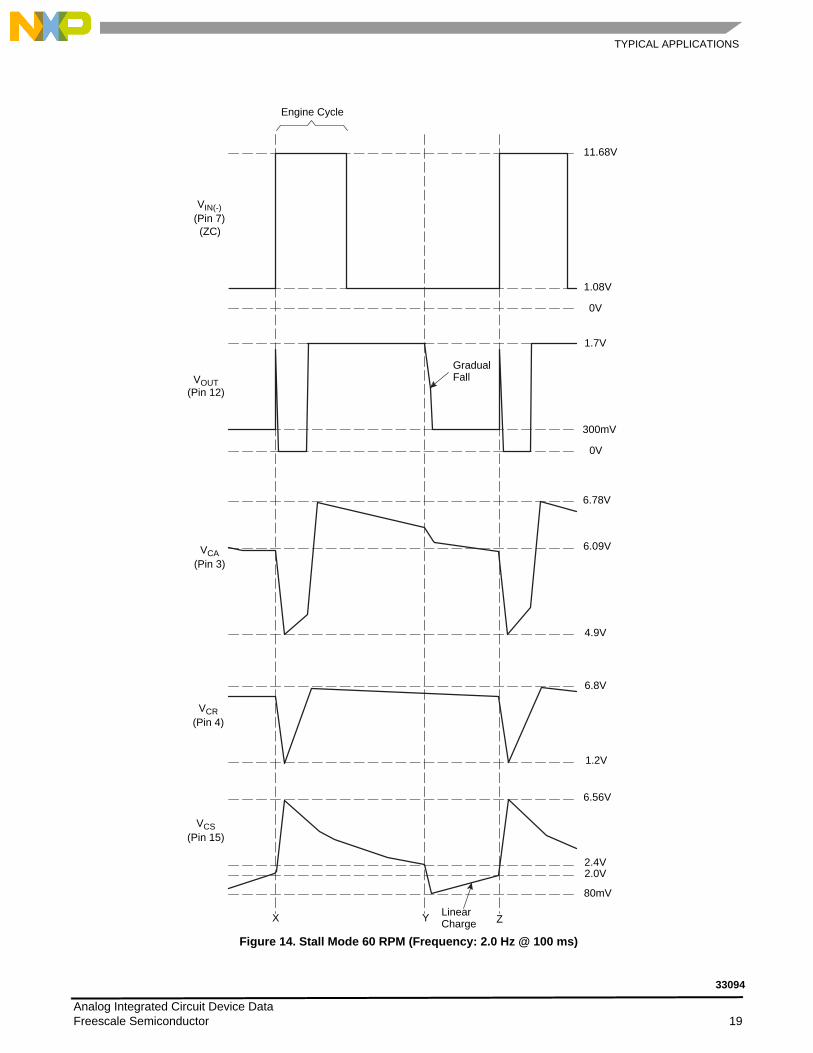
See Figure 15. At point A, a spark from the previous cycle occurs as the field around the coil collapses rapidly. At the same time ZC (VIN- > 10V) will set the 25% clock signal which commands the adaptive and ramp capacitors to discharge and the stall capacitor to charge. At point B, as the ramp capacitor voltage crosses the 1.2V (VBG) level, the 25% clock is cleared and the polarities and amplitude of the ramp and stall capacitor currents change to their appropriate levels. At this point the adaptive capacitor is discharged and begins to float. At point C, the coil turns on and ramps until the coil current is limited to 6.5 amps. The adaptive capacitor, at point D, remains discharged and the dwell is maximized to 6.5 amps because the start/run latch has yet to be set. At point E, ZC (VIN- > 10V, ZC = high) turns the coil off causing a spark to occur and at which point a new cycle begins. As the engine frequency increases, the peak voltage on the ramp capacitor at the ac signal will fall below the start mode enable threshold level. The start mode enable detector then sets the start/run latch to the run mode (CADUMP = 0) by clocking a zero into the start/run latch at the zero cross. At this time the adaptive algorithm is evoked and the adaptive capacitor is allowed to charge and discharge according to it’s other logical inputs. After normal run mode operation is entered, the start mode may not be reentered even though the ramp capacitor voltage again exceeds the start mode enable threshold. A start mode may only be evoked by a STALL signal transition from logic 1 to 0. The STALL signal transition occurs at a VIN-frequency of approximately 2.0 Hz.
The IC and circuit provides for other than normal starting procedures such as push starting the engine. Since the stall capacitor will be discharged in this low frequency mode, the
IC will provide a spark timing with a maximum retardation of about 6.5ms.
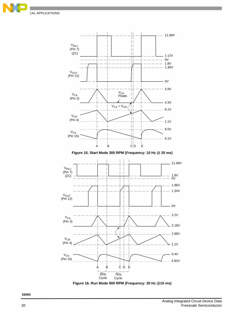
After the start mode operation is exited, the normal operation algorithm is entered and a different sequence of events dominate the IC’s performance. See Figures 16, 17, and 18. At point A, the spark from the previous cycle occurs and the 25% part of the cycle begins. During this part of the cycle, the stall capacitor will charge and the ramp and adaptive capacitors will discharge. At point B, the “not 25%” part of the cycle, also called the 75% part of the cycle, begins. The stall capacitor discharges, while the ramp capacitor charges. During this part of the cycle the adaptive capacitor floats. At point C, the ramp capacitor voltage equals the voltage on the adaptive capacitor. At this time, the coil turns on and the coil current ramps to the point where it is limited. When the coil current reaches the limit, point D, the adaptive capacitor begins to charge, until zero cross (ZC = 1logic(high)), point E. This turns the coil off and induces a spark. The 75% part of the cycle lasts until point E, at which time the cycle begins again.
The adaptive dwell algorithm causes the engine to maintain a fixed percent of excess dwell time (if possible). The mechanism that permits this involves the floating nature of the adaptive capacitor. During engine deceleration, the initial coil turn–on might occur early, but the next coil turn–on will be retarded to it’s correct location due to the % adjusted adaptive capacitor charge time. During acceleration, the coil may not charge up as early as desired the first time, however, the spark will still be correctly slaved to the distributor. The side effect of this is that the adaptive capacitor will not receive as much charge time for that cycle and will have a lower average value the next cycle, thus starting the coil charging sooner, as can be seen in Figure 17. In this figure, the output voltage rises before the adaptive capacitor charge signal occurs.
See Figure 13. In the Stall mode the output is slaved by the stall capacitor. The stall capacitor can discharge completely, but starting at point X it charges during the 25% of the engine cycle (duration of when ZC is logic high = 1). At the same time a spark from the previous cycle occurs. The DWELL signal will be high as long as the engine is in stall, but falls gradually preventing a spark at point Y when the STALL goes low starting at 2.4V. The coil will be slaved to the stall capacitor, and at point Z the coil will charge to 6.5 amps as the stall capacitor charges to 2.0V. At that time the STALL comparator will trip (STALL = 0) and the DWELL signal will fall, triggering a reduced spark with some retardation (6.5ms). At this point a new cycle begins.
Analog Integrated Circuit Device Data 14 Freescale Semiconductor
33094

FUNCTIONAL DEVICE OPERATION
Each of the three different modes (Stall, Start, and Run) have their own differences. The Stall capacitor controls the output in the stall mode, however is disabled in both the start and run modes. The output is clamped longer in the start mode as compared to the run mode due to the more energy/current in the coil causing a longer/bigger spark.
Other less likely operating sequences are possible. For example, there is a possibility of VCC exceeding 15V during engine operation (High battery = logic 1). Above about 17V on VBAT, the excess current limit percentage falls to 5% to conserve IC and circuit power dissipation. Above 25V, current to the coil is disabled. Care was placed in this design to account for all possible operating modes.
Analog Integrated Circuit Device Data Freescale Semiconductor 15
33094

TYPICAL APPLICATIONSINTRODUCTION
TYPICAL APPLICATIONS
Figure 13. Typical Ignition Circuit Application
INTRODUCTION
The MC33094 is designed for engine compartment use in 12V automotive ignition applications to provide high performance control of the ignition coil when used with an appropriate Motorola Power Darlington Transistor. Engine control systems utilizing these devices for ignition coil control exhibit superior fuel efficiency and lower exhaust emissions over predecessor systems. The device is designed for single input control from a Hall sensor to determine crankshaft position.
The device, a bipolar linear integrated circuit, is built using high–density Integrated–Injection Logic (IIL) processing incorporating high current–gain PNP and NPN transistors. All module inputs are transient voltage protected through the use of resistors, capacitors, and/or zener diodes working in conjunction with internal protection elements. These elements provide protection of critical circuitry from externally induced high–voltage transients which may degrade the devices operational performance. At the module level, it is recommended the VCC pin of the device be transient decoupled using an external resistor and capacitor to work in conjunction with the on–chip internal zener string to provide
robust module protection of the device power pin. The D (Distributor input) input of module should be protected from transients through the use of an external resistor and zener diode. The Start input of the module should be decoupled through the use of two resistors and a capacitor to work in conjunction with the on–chip internal clamp (Figure 13).
The output of the device incorporates a high current–gain PNP designed to drive an external power Darlington transistor to provide control of the ignition coil. The output drive is carefully synchronized with the output from the distributor. The charging and discharging of three capacitors, external to the device, provide timing signals which program the dwell and charge time control of the ignition coil over a wide RPM range.
The timing and charge/discharge rates of the three external capacitors are accurately controlled by internal circuitry acted upon by sensor and distributor signal detection of the device.
A feedback path from the emitter of the external power Darlington transistor to the device provide monitoring of the
Ignition +VOUT
15.3k
330
0.1µ
55
18V2 6 9
4.0k
200
10
11
12
14 200
56 0.055.0W
BU931,MJE5742orMJH10012
0.1µ 0.1µ 0.1µ
0.1µ
3 4 15
7
8
13
10k
27kSW
VIN(-)
Band-GapReference
MasterBias
VCC Clamp andZener Ref.
InputComp. andNegative
Edge Filter InternalLogic
Output CurrentDriver and Limiter
CR > CAComparator
AdaptiveCapacitor
RampCapacitor
StallCapacitor
VIN(-)
ST
T
CA CR CS
S
O
CL
D
VCCGMB
Analog Integrated Circuit Device Data 16 Freescale Semiconductor
33094
TYPICAL APPLICATIONS
ignition coil current. An internal comparator of the device senses and limits the maximum ignition coil current to approximately 6.5 amps. Other circuitry within the device provides an interruption of the coil current so as to generate the spark, or slowly discharges the coil in a controlled manner so as to prevent a spark and limit the total module energy dissipation.
When the external Darlington is switched off, the Darlington collector will instantly experience a dramatic increase in voltage as a result of the collapsing field of the ignition coil (inductive kick). The external voltage divider working in conjunction with the internal device zener string and power PNP form a dynamic clamp which limits the inductive kick voltage to less than 350V. This feature protects the Darlington transistor from damaging stress or breakdown.
IGNITION CIRCUIT OPERATION DESCRIPTIONWhen initially powered up, all module capacitors start
discharged (0V). The VCC capacitor will power up first, and the IC’s internal logic latches are indeterminate. The following conditions will hold: STALL = 1, because the stall capacitor voltage is less than 2.0 V; 25% = 0, because the ramp capacitor is less than the Band Gap Reference voltage (VBG); and ICOIL = 0 amps, because the stall capacitor is at 0V.
Because 25% = 0, the ramp capacitor charges towards VR. At cranking frequencies, the ramp capacitor always exceeds the start mode threshold at the input (ZC), and therefore the stall signal resets the start mode latch upon the first ac signal (this causes the adaptive capacitor to be discharged). With the adaptive capacitor held low, very high rates of acceleration are possible. If the adaptive capacitor were allowed to adapt the dwell at low frequencies, severe limitations to engine acceleration would occur.
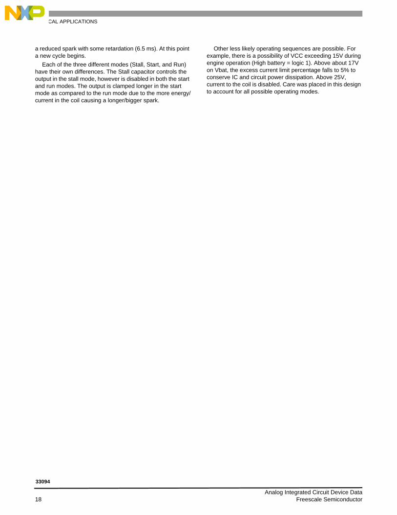
See Figure 14. At point A, a spark from the previous cycle occurs as the field around the coil collapses rapidly. At the same time ZC (ZC (input) = high(1)) will set the 25% clock signal which commands the adaptive and ramp capacitors to discharge and the stall capacitor to charge. At point B, as the ramp capacitor voltage crosses the 1.2V (VBG) level, the 25% clock is cleared and the polarities and amplitude of the ramp and stall capacitor currents change to their appropriate levels. At this point the adaptive capacitor is discharged and begins to float. At point C, the coil turns on and ramps until the coil current is limited to 6.5 amps. The adaptive capacitor, at point D, remains discharged and the dwell is maximized to 6.5 amps because the start/run latch has yet to be set. At point E, ZC (ZC = high) turns the coil off causing a spark to occur and at which point a new cycle begins. As the engine frequency increases, the peak voltage on the ramp capacitor at the ac signal will fall below the start mode enable threshold level. The start mode enable detector then sets the start/run latch to the run mode (CADUMP = 0) by clocking a zero into the start/run latch at the zero cross. At this time the adaptive algorithm is evoked and the adaptive capacitor is allowed to charge and discharge according to it’s other logical inputs. After normal run mode operation is entered, the start mode may not be reentered even though the ramp capacitor voltage again exceeds the start mode enable threshold. A start mode may only be evoked by a STALL signal transition from logic 1 to 0. The STALL signal transition occurs at a ZC frequency of approximately 2.0 Hz.
The IC and circuit provides for other than normal starting procedures such as push starting the engine. Since the stall
capacitor will be discharged in this low frequency mode, the IC will provide a spark timing with a maximum retardation of about 6.5 ms.
After the start mode operation is exited, the normal operation algorithm is entered and a different sequence of events dominate the IC’s performance. See Figures 16, Figures 17 and Figures 18. At point A, the spark from the previous cycle occurs and the 25% part of the cycle begins. During this part of the cycle, the stall capacitor will charge and the ramp and adaptive capacitors will discharge. At point B, the “not 25%” part of the cycle, also called the 75% part of the cycle, begins. The stall capacitor discharges, while the ramp capacitor charges. During this part of the cycle the adaptive capacitor floats. At point C, the ramp capacitor voltage equals the voltage on the adaptive capacitor. At this time, the coil turns on and the coil current ramps to the point where it is limited. When the coil current reaches the limit, point D, the adaptive capacitor begins to charge, until zero cross (ZC = 1logic(high)), point E. This turns the coil off and induces a spark. The 75% part of the cycle lasts until point E, at which time the cycle begins again.
The adaptive dwell algorithm causes the engine to maintain a fixed percent of excess dwell time (if possible). The mechanism that permits this involves the floating nature of the adaptive capacitor. During engine deceleration, the initial coil turn–on might occur early, but the next coil turn–on will be retarded to it’s correct location due to the % adjusted adaptive capacitor charge time. During acceleration, the coil may not charge up as early as desired the first time, however, the spark will still be correctly slaved to the distributor. The side effect of this is that the adaptive capacitor will not receive as much charge time for that cycle and will have a lower average value the next cycle, thus starting the coil charging sooner, as can be seen in Figure 18. In this figure, the output voltage rises before the adaptive capacitor charge signal occurs.
See Figure 14. In the Stall mode the output is slaved by the stall capacitor. The stall capacitor can discharge completely, but starting at point X it charges during the 25% of the engine cycle (duration of when ZC is logic high = 1). At the same time a spark from the previous cycle occurs. The DWELL signal will be high as long as the engine is in stall, but falls gradually preventing a spark at point Y when the STALL goes low starting at 2.4V. The coil will be slaved to the stall capacitor, and at point Z the coil will charge to 6.5 amps as the stall capacitor charges to 2.0V. At that time the STALL comparator will trip (STALL = 0) and the DWELL signal will fall, triggering
Analog Integrated Circuit Device Data Freescale Semiconductor 17
33094
TYPICAL APPLICATIONS
a reduced spark with some retardation (6.5 ms). At this point a new cycle begins.
Each of the three different modes (Stall, Start, and Run) have their own differences. The Stall capacitor controls the output in the stall mode, however is disabled in both the start and run modes. The output is clamped longer in the start mode as compared to the run mode due to the more energy/current in the coil causing a longer/bigger spark.
Other less likely operating sequences are possible. For example, there is a possibility of VCC exceeding 15V during engine operation (High battery = logic 1). Above about 17V on Vbat, the excess current limit percentage falls to 5% to conserve IC and circuit power dissipation. Above 25V, current to the coil is disabled. Care was placed in this design to account for all possible operating modes.
Analog Integrated Circuit Device Data 18 Freescale Semiconductor
33094
TYPICAL APPLICATIONS
Figure 14. Stall Mode 60 RPM (Frequency: 2.0 Hz @ 100 ms)
Engine Cycle
VIN(-)(Pin 7)
VOUT(Pin 12)
VCA(Pin 3)
VCR(Pin 4)
VCS(Pin 15)
X Y ZLinearCharge
GradualFall
11.68V
1.08V
0V
1.7V
300mV
0V
6.78V
6.09V
4.9V
6.8V
1.2V
6.56V
2.4V2.0V
80mV
(ZC)
Analog Integrated Circuit Device Data Freescale Semiconductor 19
33094
TYPICAL APPLICATIONS
Figure 15. Start Mode 300 RPM (Frequency: 10 Hz @ 20 ms)
Figure 16. Run Mode 900 RPM (Frequency: 30 Hz @10 ms)
VOUT(Pin 12)
VCA(Pin 3)
VCR(Pin 4)
VIN(-)(Pin 7)
VCS(Pin 15)
11.68V
1.12V0V1.8V1.36V
0V
5.9V
4.3V
6.1V
1.1V
6.5V
5.1V
VCAFloats
VCA = VCR
A B C D E
(ZC)
VOUT(Pin 12)
VCA(Pin 3)
VCR(Pin 4)
VIN(-)(Pin 7)
VCS(Pin 15)
11.68V
1.8V0V
1.86V
1.34V
0V
2.2V
2.18V
2.98V
1.1V
6.4V
5.82V
A B C D E
25%Cycle
75%Cycle
(ZC)
Analog Integrated Circuit Device Data 20 Freescale Semiconductor
33094
TYPICAL APPLICATIONS
Figure 17. Run Mode 2000 RPM (Frequency: 66.67 Hz @ 5.0 ms)
Figure 18. Run Mode 5000 RPM (Frequency: 166.67 Hz @ 2.0 ms)
VOUT(Pin 12)
VCA(Pin 3)
VCR(Pin 4)
VIN(-)(Pin 7)
VCS(Pin 15)
A B C D E
VCA = VCR
11.68V
1.8V
1.36V
1.724V
1.5V1.46V2.0V
1.08V6.42V6.36V
6.06V
0V
1.84V0V
(ZC)
VOUT(Pin 12)
VCA(Pin 3)
VCR(Pin 4)
VIN(-)(Pin 7)
VCS(Pin 15)
VCA = VCR
A B C D E
12.2V
1.8V
1.86V
1.31V
1.17V1.13V1.48V
1.12V
6.53V6.51V
6.46V
0V
0V
(ZC)
Analog Integrated Circuit Device Data Freescale Semiconductor 21
33094
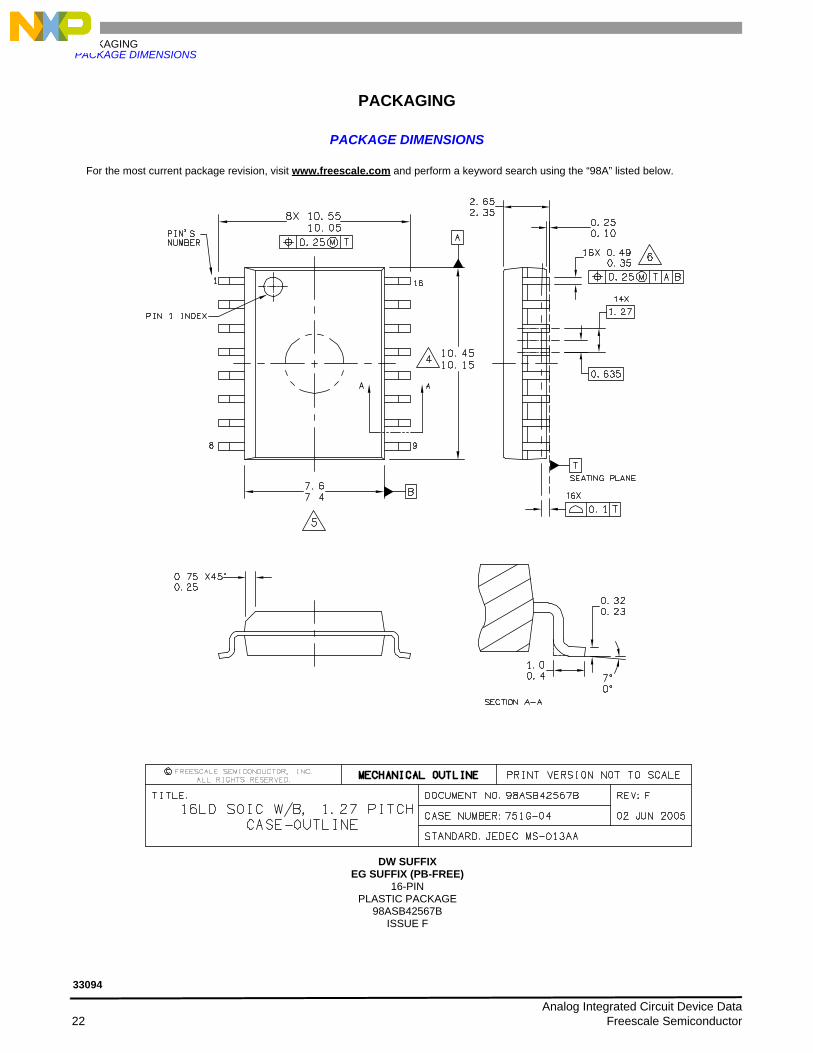
PACKAGINGPACKAGE DIMENSIONS
PACKAGING
PACKAGE DIMENSIONS
For the most current package revision, visit www.freescale.com and perform a keyword search using the “98A” listed below.
DW SUFFIXEG SUFFIX (PB-FREE)
16-PIN PLASTIC PACKAGE
98ASB42567BISSUE F
Analog Integrated Circuit Device Data 22 Freescale Semiconductor
33094
REVISION HISTORY
REVISION HISTORY
REVISION DATE DESCRIPTION OF CHANGES
1.0 10/2006 • Initial Release• Converted to Freescale format• Added MCZ33094EG/R2 to the Ordering Information• Removed Peak Package Reflow Temperature During Reflow (solder reflow) parameter from
Maximum Ratings on page 4.• Added note Freescale’s Package Reflow capability meets Pb-free requirements for JEDEC
standard J-STD-020C. For Peak Package Reflow Temperature and Moisture Sensitivity Levels (MSL), Go to www.freescale.com, search by part number [e.g. remove prefixes/suffixes and enter the core ID to view all orderable parts. (i.e. MC33xxxD enter 33xxx), and review parametrics. on page 4
Analog Integrated Circuit Device Data Freescale Semiconductor 23
33094

MC33094Rev. 1.010/2006
Information in this document is provided solely to enable system and software implementers to use Freescale Semiconductor products. There are no express or implied copyright licenses granted hereunder to design or fabricate any integrated circuits or integrated circuits based on the information in this document.
Freescale Semiconductor reserves the right to make changes without further notice to any products herein. Freescale Semiconductor makes no warranty, representation or guarantee regarding the suitability of its products for any particular purpose, nor does Freescale Semiconductor assume any liability arising out of the application or use of any product or circuit, and specifically disclaims any and all liability, including without limitation consequential or incidental damages. “Typical” parameters that may be provided in Freescale Semiconductor data sheets and/or specifications can and do vary in different applications and actual performance may vary over time. All operating parameters, including “Typicals”, must be validated for each customer application by customer’s technical experts. Freescale Semiconductor does not convey any license under its patent rights nor the rights of others. Freescale Semiconductor products are not designed, intended, or authorized for use as components in systems intended for surgical implant into the body, or other applications intended to support or sustain life, or for any other application in which the failure of the Freescale Semiconductor product could create a situation where personal injury or death may occur. Should Buyer purchase or use Freescale Semiconductor products for any such unintended or unauthorized application, Buyer shall indemnify and hold Freescale Semiconductor and its officers, employees, subsidiaries, affiliates, and distributors harmless against all claims, costs, damages, and expenses, and reasonable attorney fees arising out of, directly or indirectly, any claim of personal injury or death associated with such unintended or unauthorized use, even if such claim alleges that Freescale Semiconductor was negligent regarding the design or manufacture of the part.
Freescale™ and the Freescale logo are trademarks of Freescale Semiconductor, Inc. All other product or service names are the property of their respective owners.© Freescale Semiconductor, Inc., 2007. All rights reserved.
How to Reach Us:
Home Page:www.freescale.com
E-mail:[email protected]
USA/Europe or Locations Not Listed:Freescale SemiconductorTechnical Information Center, CH3701300 N. Alma School Road Chandler, Arizona 85224 +1-800-521-6274 or [email protected]
Europe, Middle East, and Africa:Freescale Halbleiter Deutschland GmbHTechnical Information CenterSchatzbogen 781829 Muenchen, Germany+44 1296 380 456 (English)+46 8 52200080 (English)+49 89 92103 559 (German)+33 1 69 35 48 48 (French)[email protected]
Japan:Freescale Semiconductor Japan Ltd. Headquarters ARCO Tower 15F 1-8-1, Shimo-Meguro, Meguro-ku, Tokyo 153-0064 Japan 0120 191014 or +81 3 5437 [email protected]
Asia/Pacific:Freescale Semiconductor Hong Kong Ltd.Technical Information Center 2 Dai King Street Tai Po Industrial Estate Tai Po, N.T., Hong Kong +800 2666 [email protected]
For Literature Requests Only:Freescale Semiconductor Literature Distribution CenterP.O. Box 5405Denver, Colorado 802171-800-441-2447 or 303-675-2140Fax: [email protected]
RoHS-compliant and/or Pb-free versions of Freescale products have the functionality and electrical characteristics of their non-RoHS-compliant and/or non-Pb-free counterparts. For further information, see http://www.freescale.com or contact your Freescale sales representative.
For information on Freescale’s Environmental Products program, go to http://www.freescale.com/epp.