max20303 wearae oer anagement otion · range. applications wearable devices iot benefits and...
TRANSCRIPT

Ordering Information appears at end of data sheet.
General DescriptionThe MAX20303 is a highly integrated and programmable power management solution designed for ultra-low-power wearable applications. It is optimized for size and efficiency to enhance the value of the end product by extending battery life and shrinking the overall solution size. A flexible set of power-optimized voltage regulators, including multiple bucks, boost, buck-boost, and linear regulators, provides a high level of integration and the ability to create a fully optimized power architecture. The quiescent current of each regulator is specifically suited for 1µA (typ) to extend battery life in always-on applications.The MAX20303 includes a complete battery management solution with battery seal, charger, power path, and fuel gauge. Both thermal management and input protection are built into the charger.The device also includes a factory programmable button controller with multiple inputs that are customizable to fit specific product UX requirements.Three integrated LED current sinks are included for indicator or backlighting functions, and an ERM/LRA driver with automatic resonance tracking is capable of providing sophisticated haptic feedback to the user.The device is configurable through an I2C interface that allows for programming various functions and reading device status, including the ability to read temperature and supply voltages with the integrated ADC.This device is available in a 56-bump, 0.5mm pitch 3.71mm x 4.21mm, wafer-level package (WLP) and operates over the -40°C to +85°C extended temperature range.
Applications Wearable Devices IoT
Benefits and Features Extend Battery Use Time Between Battery Charging
• 2 x Micro-IQ Buck Regulators (<1µA IQ (typ) Each)• 220mA Output• Buck1: 0.8V to 2.375V in 25mV Steps• Buck2: 0.8V to 3.95V in 50mV Steps
• Micro-IQ LV LDO/Load Switch (1µA IQ (typ))• 1.16V to 2.0V Input Voltage• 50mA Output• 0.5V to 1.95V Output, 25mV Steps
• Micro-IQ LDO/Load Switch (1µA IQ (typ))• 1.71V to 5.5V Input Voltage• 100mA Output• 0.9V to 4V, 100mV Steps
• Micro-IQ Buck-Boost Regulator (1.3µA IQ (typ))• 250mW Output• 2.5V to 5V in 100mV Steps
Easy-to-Implement Li+ Battery Charging• Wide Fast Charge Current Range: 5mA to 500mA• Smart Power Selector
• 28V/-5.5V Tolerant Input• Programmable JEITA Current/Voltage Profiles
Minimize Solution Footprint Through High Integration• Safe Output LDO
• 15mA When CHGIN Present • 5V or 3.3V
• Haptic Driver• ERM/LRA Driver with Quick Start And Breaking• Automatic Resonance Tracking (LRA only)
Support Wide Variety of Display Options • Micro-IQ Boost Regulator (2.4µA IQ (typ))
• 300mW Output• 5V to 20V in 250mV Step
• 3 Channel Current Sinks• 20V Tolerant• Programmable from 0.6 to 30mA
Optimize System Control• Power-On/Reset Controller• Programmable Push-Button Controller• Programmable Supply Sequencing• Factory Shelf Mode• On-Chip Voltage Monitor Multiplexer and Analog-
to-Digital Converter (ADC)
19-8738; Rev 7; 2/18
MAX20303 Wearable Power Management Solution
EVALUATION KIT AVAILABLE

MAX20303 Wearable Power Management Solution
www.maximintegrated.com Maxim Integrated 2
TABLE OF CONTENTSGeneral Description . . . . . . . . . . . . . . . . . . . . . . . . . . . . . . . . . . . . . . . . . . . . . . . . . . . . . . . . . . . . . . . . . . . . . . . . . . . . 1Applications . . . . . . . . . . . . . . . . . . . . . . . . . . . . . . . . . . . . . . . . . . . . . . . . . . . . . . . . . . . . . . . . . . . . . . . . . . . . . . . . . . 1Benefits and Features . . . . . . . . . . . . . . . . . . . . . . . . . . . . . . . . . . . . . . . . . . . . . . . . . . . . . . . . . . . . . . . . . . . . . . . . . . 1Absolute Maximum Ratings . . . . . . . . . . . . . . . . . . . . . . . . . . . . . . . . . . . . . . . . . . . . . . . . . . . . . . . . . . . . . . . . . . . . . 12Package Thermal Characteristics . . . . . . . . . . . . . . . . . . . . . . . . . . . . . . . . . . . . . . . . . . . . . . . . . . . . . . . . . . . . . . . . 12Electrical Characteristics . . . . . . . . . . . . . . . . . . . . . . . . . . . . . . . . . . . . . . . . . . . . . . . . . . . . . . . . . . . . . . . . . . . . . . . 12Typical Operating Characteristics . . . . . . . . . . . . . . . . . . . . . . . . . . . . . . . . . . . . . . . . . . . . . . . . . . . . . . . . . . . . . . . . 34Bump Configuration . . . . . . . . . . . . . . . . . . . . . . . . . . . . . . . . . . . . . . . . . . . . . . . . . . . . . . . . . . . . . . . . . . . . . . . . . . . 40Bump Description. . . . . . . . . . . . . . . . . . . . . . . . . . . . . . . . . . . . . . . . . . . . . . . . . . . . . . . . . . . . . . . . . . . . . . . . . . . . . .41Typical Application Diagram. . . . . . . . . . . . . . . . . . . . . . . . . . . . . . . . . . . . . . . . . . . . . . . . . . . . . . . . . . . . . . . . . . . . . 43Detailed Description. . . . . . . . . . . . . . . . . . . . . . . . . . . . . . . . . . . . . . . . . . . . . . . . . . . . . . . . . . . . . . . . . . . . . . . . . . . 44
Power Regulation . . . . . . . . . . . . . . . . . . . . . . . . . . . . . . . . . . . . . . . . . . . . . . . . . . . . . . . . . . . . . . . . . . . . . . . . . . . 44Power Switch and Reset Control . . . . . . . . . . . . . . . . . . . . . . . . . . . . . . . . . . . . . . . . . . . . . . . . . . . . . . . . . . . . . . . 44Power Sequencing . . . . . . . . . . . . . . . . . . . . . . . . . . . . . . . . . . . . . . . . . . . . . . . . . . . . . . . . . . . . . . . . . . . . . . . . . . 53Current Sink . . . . . . . . . . . . . . . . . . . . . . . . . . . . . . . . . . . . . . . . . . . . . . . . . . . . . . . . . . . . . . . . . . . . . . . . . . . . . . . 54System Load Switch . . . . . . . . . . . . . . . . . . . . . . . . . . . . . . . . . . . . . . . . . . . . . . . . . . . . . . . . . . . . . . . . . . . . . . . . . 54Smart Power Selector . . . . . . . . . . . . . . . . . . . . . . . . . . . . . . . . . . . . . . . . . . . . . . . . . . . . . . . . . . . . . . . . . . . . . . . . 54Input Limiter . . . . . . . . . . . . . . . . . . . . . . . . . . . . . . . . . . . . . . . . . . . . . . . . . . . . . . . . . . . . . . . . . . . . . . . . . . . . . . . 54SAR ADC/Monitor MUX . . . . . . . . . . . . . . . . . . . . . . . . . . . . . . . . . . . . . . . . . . . . . . . . . . . . . . . . . . . . . . . . . . . . . . 55JEITA Monitoring with Charger Control . . . . . . . . . . . . . . . . . . . . . . . . . . . . . . . . . . . . . . . . . . . . . . . . . . . . . . . . . . 55Haptic Driver . . . . . . . . . . . . . . . . . . . . . . . . . . . . . . . . . . . . . . . . . . . . . . . . . . . . . . . . . . . . . . . . . . . . . . . . . . . . . . . 55
ERM . . . . . . . . . . . . . . . . . . . . . . . . . . . . . . . . . . . . . . . . . . . . . . . . . . . . . . . . . . . . . . . . . . . . . . . . . . . . . . . . . . . 57LRA . . . . . . . . . . . . . . . . . . . . . . . . . . . . . . . . . . . . . . . . . . . . . . . . . . . . . . . . . . . . . . . . . . . . . . . . . . . . . . . . . . . 57Driver Amplitude . . . . . . . . . . . . . . . . . . . . . . . . . . . . . . . . . . . . . . . . . . . . . . . . . . . . . . . . . . . . . . . . . . . . . . . . . 57Automatic Level Compensation . . . . . . . . . . . . . . . . . . . . . . . . . . . . . . . . . . . . . . . . . . . . . . . . . . . . . . . . . . . . . . 57Haptic UVLO . . . . . . . . . . . . . . . . . . . . . . . . . . . . . . . . . . . . . . . . . . . . . . . . . . . . . . . . . . . . . . . . . . . . . . . . . . . . 57Vibration Timeout . . . . . . . . . . . . . . . . . . . . . . . . . . . . . . . . . . . . . . . . . . . . . . . . . . . . . . . . . . . . . . . . . . . . . . . . 57Overcurrent/Thermal Protection . . . . . . . . . . . . . . . . . . . . . . . . . . . . . . . . . . . . . . . . . . . . . . . . . . . . . . . . . . . . . 57Haptic Driver Lock . . . . . . . . . . . . . . . . . . . . . . . . . . . . . . . . . . . . . . . . . . . . . . . . . . . . . . . . . . . . . . . . . . . . . . . . 58
Interface Modes . . . . . . . . . . . . . . . . . . . . . . . . . . . . . . . . . . . . . . . . . . . . . . . . . . . . . . . . . . . . . . . . . . . . . . . . . . . . 58Pure-PWM (PPWM). . . . . . . . . . . . . . . . . . . . . . . . . . . . . . . . . . . . . . . . . . . . . . . . . . . . . . . . . . . . . . . . . . . . . . . 58Real-Time I2C (RTI2C). . . . . . . . . . . . . . . . . . . . . . . . . . . . . . . . . . . . . . . . . . . . . . . . . . . . . . . . . . . . . . . . . . . . . 58External Triggered Stored Pattern (ETRG) . . . . . . . . . . . . . . . . . . . . . . . . . . . . . . . . . . . . . . . . . . . . . . . . . . . . . 58RAM Stored Haptic Pattern (RAMHP) . . . . . . . . . . . . . . . . . . . . . . . . . . . . . . . . . . . . . . . . . . . . . . . . . . . . . . . . 58
Fuel Gauge . . . . . . . . . . . . . . . . . . . . . . . . . . . . . . . . . . . . . . . . . . . . . . . . . . . . . . . . . . . . . . . . . . . . . . . . . . . . . . . . 61ModelGauge Theory of Operation. . . . . . . . . . . . . . . . . . . . . . . . . . . . . . . . . . . . . . . . . . . . . . . . . . . . . . . . . . . . 61Fuel-Gauge Performance . . . . . . . . . . . . . . . . . . . . . . . . . . . . . . . . . . . . . . . . . . . . . . . . . . . . . . . . . . . . . . . . . . 61Battery Voltage and State of Charge. . . . . . . . . . . . . . . . . . . . . . . . . . . . . . . . . . . . . . . . . . . . . . . . . . . . . . . . . . 62

MAX20303 Wearable Power Management Solution
www.maximintegrated.com Maxim Integrated 3
TABLE OF CONTENTS (CONTINUED)Temperature Compensation . . . . . . . . . . . . . . . . . . . . . . . . . . . . . . . . . . . . . . . . . . . . . . . . . . . . . . . . . . . . . . . . 62Impact of Empty-Voltage Selection . . . . . . . . . . . . . . . . . . . . . . . . . . . . . . . . . . . . . . . . . . . . . . . . . . . . . . . . . . . 62Battery Insertion. . . . . . . . . . . . . . . . . . . . . . . . . . . . . . . . . . . . . . . . . . . . . . . . . . . . . . . . . . . . . . . . . . . . . . . . . . 62Battery Insertion Debounce. . . . . . . . . . . . . . . . . . . . . . . . . . . . . . . . . . . . . . . . . . . . . . . . . . . . . . . . . . . . . . . . . 62Battery Swap Detection . . . . . . . . . . . . . . . . . . . . . . . . . . . . . . . . . . . . . . . . . . . . . . . . . . . . . . . . . . . . . . . . . . . . 62Quick-Start . . . . . . . . . . . . . . . . . . . . . . . . . . . . . . . . . . . . . . . . . . . . . . . . . . . . . . . . . . . . . . . . . . . . . . . . . . . . . . 62Power-On Reset (POR) . . . . . . . . . . . . . . . . . . . . . . . . . . . . . . . . . . . . . . . . . . . . . . . . . . . . . . . . . . . . . . . . . . . . 62Hibernate Mode . . . . . . . . . . . . . . . . . . . . . . . . . . . . . . . . . . . . . . . . . . . . . . . . . . . . . . . . . . . . . . . . . . . . . . . . . . 63Alert Interrupt . . . . . . . . . . . . . . . . . . . . . . . . . . . . . . . . . . . . . . . . . . . . . . . . . . . . . . . . . . . . . . . . . . . . . . . . . . . . 63Sleep Mode . . . . . . . . . . . . . . . . . . . . . . . . . . . . . . . . . . . . . . . . . . . . . . . . . . . . . . . . . . . . . . . . . . . . . . . . . . . . . 63
I2C Interface . . . . . . . . . . . . . . . . . . . . . . . . . . . . . . . . . . . . . . . . . . . . . . . . . . . . . . . . . . . . . . . . . . . . . . . . . . . . . . 63Applications Information. . . . . . . . . . . . . . . . . . . . . . . . . . . . . . . . . . . . . . . . . . . . . . . . . . . . . . . . . . . . . . . . . . . . . . . . 63
I2C Interface . . . . . . . . . . . . . . . . . . . . . . . . . . . . . . . . . . . . . . . . . . . . . . . . . . . . . . . . . . . . . . . . . . . . . . . . . . . . . . . 63Start, Stop, And Repeated Start Conditions . . . . . . . . . . . . . . . . . . . . . . . . . . . . . . . . . . . . . . . . . . . . . . . . . . . . 63Slave Address . . . . . . . . . . . . . . . . . . . . . . . . . . . . . . . . . . . . . . . . . . . . . . . . . . . . . . . . . . . . . . . . . . . . . . . . . . . 64Bit Transfer. . . . . . . . . . . . . . . . . . . . . . . . . . . . . . . . . . . . . . . . . . . . . . . . . . . . . . . . . . . . . . . . . . . . . . . . . . . . . . 64Single-Byte Write . . . . . . . . . . . . . . . . . . . . . . . . . . . . . . . . . . . . . . . . . . . . . . . . . . . . . . . . . . . . . . . . . . . . . . . . . 64Burst Write . . . . . . . . . . . . . . . . . . . . . . . . . . . . . . . . . . . . . . . . . . . . . . . . . . . . . . . . . . . . . . . . . . . . . . . . . . . . . . 64Single Byte Read . . . . . . . . . . . . . . . . . . . . . . . . . . . . . . . . . . . . . . . . . . . . . . . . . . . . . . . . . . . . . . . . . . . . . . . . . 65Burst Read . . . . . . . . . . . . . . . . . . . . . . . . . . . . . . . . . . . . . . . . . . . . . . . . . . . . . . . . . . . . . . . . . . . . . . . . . . . . . . 66Acknowledge Bits. . . . . . . . . . . . . . . . . . . . . . . . . . . . . . . . . . . . . . . . . . . . . . . . . . . . . . . . . . . . . . . . . . . . . . . . . 66
Application Processor Interface . . . . . . . . . . . . . . . . . . . . . . . . . . . . . . . . . . . . . . . . . . . . . . . . . . . . . . . . . . . . . . . . 67AP Write . . . . . . . . . . . . . . . . . . . . . . . . . . . . . . . . . . . . . . . . . . . . . . . . . . . . . . . . . . . . . . . . . . . . . . . . . . . . . . . . 67AP Read. . . . . . . . . . . . . . . . . . . . . . . . . . . . . . . . . . . . . . . . . . . . . . . . . . . . . . . . . . . . . . . . . . . . . . . . . . . . . . . . 67AP Launch . . . . . . . . . . . . . . . . . . . . . . . . . . . . . . . . . . . . . . . . . . . . . . . . . . . . . . . . . . . . . . . . . . . . . . . . . . . . . . 67Write-Protected Commands and Fields. . . . . . . . . . . . . . . . . . . . . . . . . . . . . . . . . . . . . . . . . . . . . . . . . . . . . . . . 67
Direct Access I2C Register Map . . . . . . . . . . . . . . . . . . . . . . . . . . . . . . . . . . . . . . . . . . . . . . . . . . . . . . . . . . . . . . . . . 68Direct Access I2C Register Descriptions . . . . . . . . . . . . . . . . . . . . . . . . . . . . . . . . . . . . . . . . . . . . . . . . . . . . . . . . . . . 70
Interrupt Registers. . . . . . . . . . . . . . . . . . . . . . . . . . . . . . . . . . . . . . . . . . . . . . . . . . . . . . . . . . . . . . . . . . . . . . . . . . . 70Status Registers . . . . . . . . . . . . . . . . . . . . . . . . . . . . . . . . . . . . . . . . . . . . . . . . . . . . . . . . . . . . . . . . . . . . . . . . . . . . 71Interrupt Mask Registers. . . . . . . . . . . . . . . . . . . . . . . . . . . . . . . . . . . . . . . . . . . . . . . . . . . . . . . . . . . . . . . . . . . . . . 75AP Interface Registers . . . . . . . . . . . . . . . . . . . . . . . . . . . . . . . . . . . . . . . . . . . . . . . . . . . . . . . . . . . . . . . . . . . . . . . 78LDO Direct Register . . . . . . . . . . . . . . . . . . . . . . . . . . . . . . . . . . . . . . . . . . . . . . . . . . . . . . . . . . . . . . . . . . . . . . . . . 80MPC Direct Registers . . . . . . . . . . . . . . . . . . . . . . . . . . . . . . . . . . . . . . . . . . . . . . . . . . . . . . . . . . . . . . . . . . . . . . . . 81Haptic RAM Registers . . . . . . . . . . . . . . . . . . . . . . . . . . . . . . . . . . . . . . . . . . . . . . . . . . . . . . . . . . . . . . . . . . . . . . . 82LED Direct Registers . . . . . . . . . . . . . . . . . . . . . . . . . . . . . . . . . . . . . . . . . . . . . . . . . . . . . . . . . . . . . . . . . . . . . . . . 83Haptic Direct Registers . . . . . . . . . . . . . . . . . . . . . . . . . . . . . . . . . . . . . . . . . . . . . . . . . . . . . . . . . . . . . . . . . . . . . . . 85
AP Command Register Descriptions . . . . . . . . . . . . . . . . . . . . . . . . . . . . . . . . . . . . . . . . . . . . . . . . . . . . . . . . . . . . . . 88

MAX20303 Wearable Power Management Solution
www.maximintegrated.com Maxim Integrated 4
TABLE OF CONTENTS (CONTINUED)GPIO Config Commands . . . . . . . . . . . . . . . . . . . . . . . . . . . . . . . . . . . . . . . . . . . . . . . . . . . . . . . . . . . . . . . . . . . . . 88Input Current Limit Commands. . . . . . . . . . . . . . . . . . . . . . . . . . . . . . . . . . . . . . . . . . . . . . . . . . . . . . . . . . . . . . . . . 93Thermal Shutdown Configuration Commands . . . . . . . . . . . . . . . . . . . . . . . . . . . . . . . . . . . . . . . . . . . . . . . . . . . . . 94Charger Configuratoin Commands . . . . . . . . . . . . . . . . . . . . . . . . . . . . . . . . . . . . . . . . . . . . . . . . . . . . . . . . . . . . . . 95Boost Configuration Commands. . . . . . . . . . . . . . . . . . . . . . . . . . . . . . . . . . . . . . . . . . . . . . . . . . . . . . . . . . . . . . . 104Buck Configuration Commands . . . . . . . . . . . . . . . . . . . . . . . . . . . . . . . . . . . . . . . . . . . . . . . . . . . . . . . . . . . . . . . 106LDO Configuration Commands. . . . . . . . . . . . . . . . . . . . . . . . . . . . . . . . . . . . . . . . . . . . . . . . . . . . . . . . . . . . . . . . 112Charge Pump Configuration Commands . . . . . . . . . . . . . . . . . . . . . . . . . . . . . . . . . . . . . . . . . . . . . . . . . . . . . . . . 116SFOUT Configuration Commands . . . . . . . . . . . . . . . . . . . . . . . . . . . . . . . . . . . . . . . . . . . . . . . . . . . . . . . . . . . . . 117MON Mux Configuration Commands . . . . . . . . . . . . . . . . . . . . . . . . . . . . . . . . . . . . . . . . . . . . . . . . . . . . . . . . . . . 119Buck-Boost Configuration Commands . . . . . . . . . . . . . . . . . . . . . . . . . . . . . . . . . . . . . . . . . . . . . . . . . . . . . . . . . . 121Haptic Configuration Commands . . . . . . . . . . . . . . . . . . . . . . . . . . . . . . . . . . . . . . . . . . . . . . . . . . . . . . . . . . . . . . 124Power and Reset Commands . . . . . . . . . . . . . . . . . . . . . . . . . . . . . . . . . . . . . . . . . . . . . . . . . . . . . . . . . . . . . . . . . 137
Register Summary . . . . . . . . . . . . . . . . . . . . . . . . . . . . . . . . . . . . . . . . . . . . . . . . . . . . . . . . . . . . . . . . . . . . . . . . . . . 140VCELL Register (0x02) . . . . . . . . . . . . . . . . . . . . . . . . . . . . . . . . . . . . . . . . . . . . . . . . . . . . . . . . . . . . . . . . . . . . . . 140SOC Register (0x04). . . . . . . . . . . . . . . . . . . . . . . . . . . . . . . . . . . . . . . . . . . . . . . . . . . . . . . . . . . . . . . . . . . . . . . . 140MODE Register (0x06) . . . . . . . . . . . . . . . . . . . . . . . . . . . . . . . . . . . . . . . . . . . . . . . . . . . . . . . . . . . . . . . . . . . . . . 140VERSION Register (0x08) . . . . . . . . . . . . . . . . . . . . . . . . . . . . . . . . . . . . . . . . . . . . . . . . . . . . . . . . . . . . . . . . . . . 140
Fuel Gauge I2C Registers . . . . . . . . . . . . . . . . . . . . . . . . . . . . . . . . . . . . . . . . . . . . . . . . . . . . . . . . . . . . . . . . . . . . . 140HIBRT Register (0x0A) . . . . . . . . . . . . . . . . . . . . . . . . . . . . . . . . . . . . . . . . . . . . . . . . . . . . . . . . . . . . . . . . . . . . . . 141CONFIG Register (0x0C) . . . . . . . . . . . . . . . . . . . . . . . . . . . . . . . . . . . . . . . . . . . . . . . . . . . . . . . . . . . . . . . . . . . . 141VALRT Register (0x14) . . . . . . . . . . . . . . . . . . . . . . . . . . . . . . . . . . . . . . . . . . . . . . . . . . . . . . . . . . . . . . . . . . . . . . 142CRATE Register (0x16). . . . . . . . . . . . . . . . . . . . . . . . . . . . . . . . . . . . . . . . . . . . . . . . . . . . . . . . . . . . . . . . . . . . . . 142VRESET/ID Register (0x18) . . . . . . . . . . . . . . . . . . . . . . . . . . . . . . . . . . . . . . . . . . . . . . . . . . . . . . . . . . . . . . . . . . 142STATUS Register (0x1A). . . . . . . . . . . . . . . . . . . . . . . . . . . . . . . . . . . . . . . . . . . . . . . . . . . . . . . . . . . . . . . . . . . . . 143
Reset Indicator: . . . . . . . . . . . . . . . . . . . . . . . . . . . . . . . . . . . . . . . . . . . . . . . . . . . . . . . . . . . . . . . . . . . . . . . . . 143Alert Descriptors: . . . . . . . . . . . . . . . . . . . . . . . . . . . . . . . . . . . . . . . . . . . . . . . . . . . . . . . . . . . . . . . . . . . . . . . . 143Enable or Disable VRESET Alert: . . . . . . . . . . . . . . . . . . . . . . . . . . . . . . . . . . . . . . . . . . . . . . . . . . . . . . . . . . . 143
TABLE Registers (0x40 to 0x7F) . . . . . . . . . . . . . . . . . . . . . . . . . . . . . . . . . . . . . . . . . . . . . . . . . . . . . . . . . . . . . . 143CMD Register (0xFE) . . . . . . . . . . . . . . . . . . . . . . . . . . . . . . . . . . . . . . . . . . . . . . . . . . . . . . . . . . . . . . . . . . . . . . . 143
Ordering Information . . . . . . . . . . . . . . . . . . . . . . . . . . . . . . . . . . . . . . . . . . . . . . . . . . . . . . . . . . . . . . . . . . . . . . . . . 146Chip Information. . . . . . . . . . . . . . . . . . . . . . . . . . . . . . . . . . . . . . . . . . . . . . . . . . . . . . . . . . . . . . . . . . . . . . . . . . . . . 146Package Information . . . . . . . . . . . . . . . . . . . . . . . . . . . . . . . . . . . . . . . . . . . . . . . . . . . . . . . . . . . . . . . . . . . . . . . . . 146Revision History . . . . . . . . . . . . . . . . . . . . . . . . . . . . . . . . . . . . . . . . . . . . . . . . . . . . . . . . . . . . . . . . . . . . . . . . . . . . . .147

MAX20303 Wearable Power Management Solution
www.maximintegrated.com Maxim Integrated 5
LIST OF FIGURESFigure 1a. PwrRstCfg = 0000 or 0001. . . . . . . . . . . . . . . . . . . . . . . . . . . . . . . . . . . . . . . . . . . . . . . . . . . . . . . . . . . . . 45Figure 1b. PwrRstCfg = 0010 or 0011 . . . . . . . . . . . . . . . . . . . . . . . . . . . . . . . . . . . . . . . . . . . . . . . . . . . . . . . . . . . . . 46Figure 1c. PwrRstCfg = 0100 or 0101 . . . . . . . . . . . . . . . . . . . . . . . . . . . . . . . . . . . . . . . . . . . . . . . . . . . . . . . . . . . . . 47Figure 1d. PwrRstCfg = 0110 . . . . . . . . . . . . . . . . . . . . . . . . . . . . . . . . . . . . . . . . . . . . . . . . . . . . . . . . . . . . . . . . . . . . 48Figure 1e. PwrRstCfg = 0111 . . . . . . . . . . . . . . . . . . . . . . . . . . . . . . . . . . . . . . . . . . . . . . . . . . . . . . . . . . . . . . . . . . . . 49Figure 1f. PwrRstCfg = 1000 . . . . . . . . . . . . . . . . . . . . . . . . . . . . . . . . . . . . . . . . . . . . . . . . . . . . . . . . . . . . . . . . . . . . 50Figure 2. The full MAX20303 Boot Sequence. . . . . . . . . . . . . . . . . . . . . . . . . . . . . . . . . . . . . . . . . . . . . . . . . . . . . . . 52Figure 3. Reset Sequence Programming. . . . . . . . . . . . . . . . . . . . . . . . . . . . . . . . . . . . . . . . . . . . . . . . . . . . . . . . . . . 53Figure 4a. Sample JEITA Pre Charge Profile . . . . . . . . . . . . . . . . . . . . . . . . . . . . . . . . . . . . . . . . . . . . . . . . . . . . . . . 55Figure 4b. Sample JEITA Fast Charge Profile . . . . . . . . . . . . . . . . . . . . . . . . . . . . . . . . . . . . . . . . . . . . . . . . . . . . . . . 55Figure 4c. Sample JEITA Maintain Charge Profile . . . . . . . . . . . . . . . . . . . . . . . . . . . . . . . . . . . . . . . . . . . . . . . . . . . 56Figure 5. Charger State Diagram. . . . . . . . . . . . . . . . . . . . . . . . . . . . . . . . . . . . . . . . . . . . . . . . . . . . . . . . . . . . . . . . . 56Figure 6. Read and Write Processes for RAM . . . . . . . . . . . . . . . . . . . . . . . . . . . . . . . . . . . . . . . . . . . . . . . . . . . . . . 59Figure 7a. Sample Pattern Stored in RAM . . . . . . . . . . . . . . . . . . . . . . . . . . . . . . . . . . . . . . . . . . . . . . . . . . . . . . . . . 61Figure 7b. Haptic Driver Output of Stored Pattern. . . . . . . . . . . . . . . . . . . . . . . . . . . . . . . . . . . . . . . . . . . . . . . . . . . . 61Figure 8. I2C START, STOP and REPEATED START Conditions . . . . . . . . . . . . . . . . . . . . . . . . . . . . . . . . . . . . . . . 63Figure 9. Write Byte Sequence . . . . . . . . . . . . . . . . . . . . . . . . . . . . . . . . . . . . . . . . . . . . . . . . . . . . . . . . . . . . . . . . . . 64Figure 10. Burst Write Sequence. . . . . . . . . . . . . . . . . . . . . . . . . . . . . . . . . . . . . . . . . . . . . . . . . . . . . . . . . . . . . . . . . 65Figure 11. Read Byte Sequence . . . . . . . . . . . . . . . . . . . . . . . . . . . . . . . . . . . . . . . . . . . . . . . . . . . . . . . . . . . . . . . . . 65Figure 12. Burst Read Sequence. . . . . . . . . . . . . . . . . . . . . . . . . . . . . . . . . . . . . . . . . . . . . . . . . . . . . . . . . . . . . . . . . 66Figure 13. Acknowledge . . . . . . . . . . . . . . . . . . . . . . . . . . . . . . . . . . . . . . . . . . . . . . . . . . . . . . . . . . . . . . . . . . . . . . . 66Figure 14. Executing a Write Opcode and Reading the MAX20303 Response . . . . . . . . . . . . . . . . . . . . . . . . . . . . . 67Figure 15. Executing a Read Opcode and Reading the MAX20303 Response . . . . . . . . . . . . . . . . . . . . . . . . . . . . . 67Figure 16. MODE Register Format . . . . . . . . . . . . . . . . . . . . . . . . . . . . . . . . . . . . . . . . . . . . . . . . . . . . . . . . . . . . . . .141Figure 17. HIBRT Register Format. . . . . . . . . . . . . . . . . . . . . . . . . . . . . . . . . . . . . . . . . . . . . . . . . . . . . . . . . . . . . . . .141Figure 18. CONFIG Register Format . . . . . . . . . . . . . . . . . . . . . . . . . . . . . . . . . . . . . . . . . . . . . . . . . . . . . . . . . . . . . .141Figure 19. VALRT Register Format . . . . . . . . . . . . . . . . . . . . . . . . . . . . . . . . . . . . . . . . . . . . . . . . . . . . . . . . . . . . . . 142Figure 20. VRESET/ID Register Format . . . . . . . . . . . . . . . . . . . . . . . . . . . . . . . . . . . . . . . . . . . . . . . . . . . . . . . . . . 142Figure 21. STATUS Register Format . . . . . . . . . . . . . . . . . . . . . . . . . . . . . . . . . . . . . . . . . . . . . . . . . . . . . . . . . . . . . 143

MAX20303 Wearable Power Management Solution
www.maximintegrated.com Maxim Integrated 6
LIST OF TABLESTable 1. PwrRstCfg Settings . . . . . . . . . . . . . . . . . . . . . . . . . . . . . . . . . . . . . . . . . . . . . . . . . . . . . . . . . . . . . . . . . . . . 51Table 2. SAR ADC Full-Scale Voltages and Conversions. . . . . . . . . . . . . . . . . . . . . . . . . . . . . . . . . . . . . . . . . . . . . . 55Table 3. RAMHP Pattern Storage Format . . . . . . . . . . . . . . . . . . . . . . . . . . . . . . . . . . . . . . . . . . . . . . . . . . . . . . . . . . 60Table 4. HardwareID Register (0x00). . . . . . . . . . . . . . . . . . . . . . . . . . . . . . . . . . . . . . . . . . . . . . . . . . . . . . . . . . . . . . 70Table 5. FirmwareID Register (0x01) . . . . . . . . . . . . . . . . . . . . . . . . . . . . . . . . . . . . . . . . . . . . . . . . . . . . . . . . . . . . . . 70Table 6. Int0 Register (0x03) . . . . . . . . . . . . . . . . . . . . . . . . . . . . . . . . . . . . . . . . . . . . . . . . . . . . . . . . . . . . . . . . . . . . 70Table 7. Int1 Register (0x04) . . . . . . . . . . . . . . . . . . . . . . . . . . . . . . . . . . . . . . . . . . . . . . . . . . . . . . . . . . . . . . . . . . . . 70Table 8. Int2 Register (0x05) . . . . . . . . . . . . . . . . . . . . . . . . . . . . . . . . . . . . . . . . . . . . . . . . . . . . . . . . . . . . . . . . . . . . 71Table 9. Status0 Register (0x06) . . . . . . . . . . . . . . . . . . . . . . . . . . . . . . . . . . . . . . . . . . . . . . . . . . . . . . . . . . . . . . . . . 71Table 10. Status1 Register (0x07) . . . . . . . . . . . . . . . . . . . . . . . . . . . . . . . . . . . . . . . . . . . . . . . . . . . . . . . . . . . . . . . . 72Table 11. Status2 Register (0x08) . . . . . . . . . . . . . . . . . . . . . . . . . . . . . . . . . . . . . . . . . . . . . . . . . . . . . . . . . . . . . . . . 73Table 12. Status3 Register (0x09) . . . . . . . . . . . . . . . . . . . . . . . . . . . . . . . . . . . . . . . . . . . . . . . . . . . . . . . . . . . . . . . . 73Table 13. SystemError Register (0x0B) . . . . . . . . . . . . . . . . . . . . . . . . . . . . . . . . . . . . . . . . . . . . . . . . . . . . . . . . . . . . .74Table 14. IntMask0 Register (0x0C). . . . . . . . . . . . . . . . . . . . . . . . . . . . . . . . . . . . . . . . . . . . . . . . . . . . . . . . . . . . . . . 75Table 15. IntMask1 Register (0x0D). . . . . . . . . . . . . . . . . . . . . . . . . . . . . . . . . . . . . . . . . . . . . . . . . . . . . . . . . . . . . . . 76Table 16. IntMask2 Register (0x0E). . . . . . . . . . . . . . . . . . . . . . . . . . . . . . . . . . . . . . . . . . . . . . . . . . . . . . . . . . . . . . . 77Table 17. APDataOut0 Register (0x0F) . . . . . . . . . . . . . . . . . . . . . . . . . . . . . . . . . . . . . . . . . . . . . . . . . . . . . . . . . . . . 78Table 18. APDataOut1 Register (0x10) . . . . . . . . . . . . . . . . . . . . . . . . . . . . . . . . . . . . . . . . . . . . . . . . . . . . . . . . . . . . 78Table 19. APDataOut2 Register (0x11) . . . . . . . . . . . . . . . . . . . . . . . . . . . . . . . . . . . . . . . . . . . . . . . . . . . . . . . . . . . . 78Table 20. APDataOut3 Register (0x12) . . . . . . . . . . . . . . . . . . . . . . . . . . . . . . . . . . . . . . . . . . . . . . . . . . . . . . . . . . . . 78Table 21. APDataOut4 Register (0x13) . . . . . . . . . . . . . . . . . . . . . . . . . . . . . . . . . . . . . . . . . . . . . . . . . . . . . . . . . . . . 78Table 22. APDataOut5 Register (0x14) . . . . . . . . . . . . . . . . . . . . . . . . . . . . . . . . . . . . . . . . . . . . . . . . . . . . . . . . . . . . 79Table 23. APDataOut6 Register (0x15) . . . . . . . . . . . . . . . . . . . . . . . . . . . . . . . . . . . . . . . . . . . . . . . . . . . . . . . . . . . . 79Table 24. APCmdOut Register (0x17) . . . . . . . . . . . . . . . . . . . . . . . . . . . . . . . . . . . . . . . . . . . . . . . . . . . . . . . . . . . . . 79Table 25. APResponse Register (0x18) . . . . . . . . . . . . . . . . . . . . . . . . . . . . . . . . . . . . . . . . . . . . . . . . . . . . . . . . . . . . 79Table 26. APDataIn0 Register (0x19). . . . . . . . . . . . . . . . . . . . . . . . . . . . . . . . . . . . . . . . . . . . . . . . . . . . . . . . . . . . . . 79Table 27. APDataIn1 Register (0x1A). . . . . . . . . . . . . . . . . . . . . . . . . . . . . . . . . . . . . . . . . . . . . . . . . . . . . . . . . . . . . . 79Table 28. APDataIn2 Register (0x1B) . . . . . . . . . . . . . . . . . . . . . . . . . . . . . . . . . . . . . . . . . . . . . . . . . . . . . . . . . . . . . 80Table 29. APDataIn3 Register (0x1C) . . . . . . . . . . . . . . . . . . . . . . . . . . . . . . . . . . . . . . . . . . . . . . . . . . . . . . . . . . . . . 80Table 30. APDataIn4 Register (0x1D) . . . . . . . . . . . . . . . . . . . . . . . . . . . . . . . . . . . . . . . . . . . . . . . . . . . . . . . . . . . . . 80Table 31. APDataIn5 Register (0x1E) . . . . . . . . . . . . . . . . . . . . . . . . . . . . . . . . . . . . . . . . . . . . . . . . . . . . . . . . . . . . . 80Table 32. LDODirect Register (0x20). . . . . . . . . . . . . . . . . . . . . . . . . . . . . . . . . . . . . . . . . . . . . . . . . . . . . . . . . . . . . . 80Table 33. MPCDirectWrite Register (0x21) . . . . . . . . . . . . . . . . . . . . . . . . . . . . . . . . . . . . . . . . . . . . . . . . . . . . . . . . . 81Table 34. MPCDirectRead Register (0x22) . . . . . . . . . . . . . . . . . . . . . . . . . . . . . . . . . . . . . . . . . . . . . . . . . . . . . . . . . 81Table 35. HptRAMAddr Register (0x28) . . . . . . . . . . . . . . . . . . . . . . . . . . . . . . . . . . . . . . . . . . . . . . . . . . . . . . . . . . . 82

MAX20303 Wearable Power Management Solution
www.maximintegrated.com Maxim Integrated 7
LIST OF TABLES (CONTINUED)Table 36. HptRAMDataH Register (0x29) . . . . . . . . . . . . . . . . . . . . . . . . . . . . . . . . . . . . . . . . . . . . . . . . . . . . . . . . . . 82Table 37. HptRAMDataM Register (0x2A) . . . . . . . . . . . . . . . . . . . . . . . . . . . . . . . . . . . . . . . . . . . . . . . . . . . . . . . . . . 82Table 38. HptRAMDataL Register (0x2B) . . . . . . . . . . . . . . . . . . . . . . . . . . . . . . . . . . . . . . . . . . . . . . . . . . . . . . . . . . 82Table 39. LEDStepDirect Register (0x2C) . . . . . . . . . . . . . . . . . . . . . . . . . . . . . . . . . . . . . . . . . . . . . . . . . . . . . . . . . . 83Table 40. LED0Direct Register (0x2D). . . . . . . . . . . . . . . . . . . . . . . . . . . . . . . . . . . . . . . . . . . . . . . . . . . . . . . . . . . . . 83Table 41. LED1Direct Register (0x2E) . . . . . . . . . . . . . . . . . . . . . . . . . . . . . . . . . . . . . . . . . . . . . . . . . . . . . . . . . . . . . 84Table 42. LED2Direct Register (0x2F) . . . . . . . . . . . . . . . . . . . . . . . . . . . . . . . . . . . . . . . . . . . . . . . . . . . . . . . . . . . . . 84Table 43. HptDirect0 Register (0x30). . . . . . . . . . . . . . . . . . . . . . . . . . . . . . . . . . . . . . . . . . . . . . . . . . . . . . . . . . . . . . 85Table 44. HptDirect1 Register (0x31) . . . . . . . . . . . . . . . . . . . . . . . . . . . . . . . . . . . . . . . . . . . . . . . . . . . . . . . . . . . . . . 86Table 45. HptRTI2CAmp Register (0x32) . . . . . . . . . . . . . . . . . . . . . . . . . . . . . . . . . . . . . . . . . . . . . . . . . . . . . . . . . . 87Table 46. HptPatRAMAddr Register (0x33) . . . . . . . . . . . . . . . . . . . . . . . . . . . . . . . . . . . . . . . . . . . . . . . . . . . . . . . . . 87Table 47. 0x01 – GPIO_Config_Write . . . . . . . . . . . . . . . . . . . . . . . . . . . . . . . . . . . . . . . . . . . . . . . . . . . . . . . . . . . . . 88Table 48. GPIO_Config_Write Response . . . . . . . . . . . . . . . . . . . . . . . . . . . . . . . . . . . . . . . . . . . . . . . . . . . . . . . . . . 89Table 49. 0x02 – GPIO_Config_Read . . . . . . . . . . . . . . . . . . . . . . . . . . . . . . . . . . . . . . . . . . . . . . . . . . . . . . . . . . . . . 89Table 50. GPIO_Config_Read Response . . . . . . . . . . . . . . . . . . . . . . . . . . . . . . . . . . . . . . . . . . . . . . . . . . . . . . . . . . 89Table 51. 0x03 – GPIO_Control_Write. . . . . . . . . . . . . . . . . . . . . . . . . . . . . . . . . . . . . . . . . . . . . . . . . . . . . . . . . . . . . 89Table 52. GPIO_Control_Write Response . . . . . . . . . . . . . . . . . . . . . . . . . . . . . . . . . . . . . . . . . . . . . . . . . . . . . . . . . . 90Table 53. 0x04 – GPIO_Control_Read . . . . . . . . . . . . . . . . . . . . . . . . . . . . . . . . . . . . . . . . . . . . . . . . . . . . . . . . . . . . 90Table 54. GPIO_Control_Read Response. . . . . . . . . . . . . . . . . . . . . . . . . . . . . . . . . . . . . . . . . . . . . . . . . . . . . . . . . . 90Table 55. 0x06 – MPC_Config_Write . . . . . . . . . . . . . . . . . . . . . . . . . . . . . . . . . . . . . . . . . . . . . . . . . . . . . . . . . . . . . 90Table 56. MPC_Config_Write Response . . . . . . . . . . . . . . . . . . . . . . . . . . . . . . . . . . . . . . . . . . . . . . . . . . . . . . . . . . . 92Table 57. 0x07 – MPC_Config_Read . . . . . . . . . . . . . . . . . . . . . . . . . . . . . . . . . . . . . . . . . . . . . . . . . . . . . . . . . . . . . 92Table 58. MPC_Config_Read Response. . . . . . . . . . . . . . . . . . . . . . . . . . . . . . . . . . . . . . . . . . . . . . . . . . . . . . . . . . . 92Table 59. 0x10 – InputCurrent_Config_Write . . . . . . . . . . . . . . . . . . . . . . . . . . . . . . . . . . . . . . . . . . . . . . . . . . . . . . . 93Table 60. InputCurrent_Config_Write Response. . . . . . . . . . . . . . . . . . . . . . . . . . . . . . . . . . . . . . . . . . . . . . . . . . . . . 93Table 61. 0x11 – InputCurrent_Config_Read . . . . . . . . . . . . . . . . . . . . . . . . . . . . . . . . . . . . . . . . . . . . . . . . . . . . . . . 93Table 62. InputCurrent_Config_Read Response. . . . . . . . . . . . . . . . . . . . . . . . . . . . . . . . . . . . . . . . . . . . . . . . . . . . . 94Table 63. 0x12 – ThermalShutdown_Config_Read. . . . . . . . . . . . . . . . . . . . . . . . . . . . . . . . . . . . . . . . . . . . . . . . . . . 94Table 64. ThermalShutdown_Config_Read Response . . . . . . . . . . . . . . . . . . . . . . . . . . . . . . . . . . . . . . . . . . . . . . . . 94Table 65. 0x14 – Charger_Config_Write . . . . . . . . . . . . . . . . . . . . . . . . . . . . . . . . . . . . . . . . . . . . . . . . . . . . . . . . . . . 95Table 66. Charger_Config_Write Response . . . . . . . . . . . . . . . . . . . . . . . . . . . . . . . . . . . . . . . . . . . . . . . . . . . . . . . . 97Table 67. 0x15 – Charger_Config_Read . . . . . . . . . . . . . . . . . . . . . . . . . . . . . . . . . . . . . . . . . . . . . . . . . . . . . . . . . . . 97Table 68. Charger_Config_Read Response . . . . . . . . . . . . . . . . . . . . . . . . . . . . . . . . . . . . . . . . . . . . . . . . . . . . . . . . 97Table 69. 0x16 – ChargerThermalLimits_Config_Write . . . . . . . . . . . . . . . . . . . . . . . . . . . . . . . . . . . . . . . . . . . . . . . . 98Table 70. ChargerThermalLimits_Config_Write Response . . . . . . . . . . . . . . . . . . . . . . . . . . . . . . . . . . . . . . . . . . . . . 98

MAX20303 Wearable Power Management Solution
www.maximintegrated.com Maxim Integrated 8
LIST OF TABLES (CONTINUED)Table 71. 0x17 – ChargerThermalLimits_Config_Read . . . . . . . . . . . . . . . . . . . . . . . . . . . . . . . . . . . . . . . . . . . . . . . . 98Table 72. ChargerThermalLimits_Config_Read Response . . . . . . . . . . . . . . . . . . . . . . . . . . . . . . . . . . . . . . . . . . . . . 99Table 73. 0x18 – ChargerThermalReg_Config_Write . . . . . . . . . . . . . . . . . . . . . . . . . . . . . . . . . . . . . . . . . . . . . . . . . 99Table 74. ChargerThermalReg_Config_Write Response. . . . . . . . . . . . . . . . . . . . . . . . . . . . . . . . . . . . . . . . . . . . . . 102Table 75. 0x19 – ChargerThermalReg_Config_Read . . . . . . . . . . . . . . . . . . . . . . . . . . . . . . . . . . . . . . . . . . . . . . . . 102Table 76. ChargerThermalReg_Config_Read Response . . . . . . . . . . . . . . . . . . . . . . . . . . . . . . . . . . . . . . . . . . . . . 102Table 77. 0x1A – Charger_ControlWrite. . . . . . . . . . . . . . . . . . . . . . . . . . . . . . . . . . . . . . . . . . . . . . . . . . . . . . . . . . . 102Table 78. Charger_ControlWrite Response . . . . . . . . . . . . . . . . . . . . . . . . . . . . . . . . . . . . . . . . . . . . . . . . . . . . . . . . 102Table 79. 0x1B – Charger_ControlRead . . . . . . . . . . . . . . . . . . . . . . . . . . . . . . . . . . . . . . . . . . . . . . . . . . . . . . . . . . 103Table 80. Charger_Control_Read Response. . . . . . . . . . . . . . . . . . . . . . . . . . . . . . . . . . . . . . . . . . . . . . . . . . . . . . . 103Table 81. 0x1C – Charger_ JEITAHyst_ControlWrite . . . . . . . . . . . . . . . . . . . . . . . . . . . . . . . . . . . . . . . . . . . . . . . . 103Table 82. Charger_JEITAHyst_ControlWrite Response . . . . . . . . . . . . . . . . . . . . . . . . . . . . . . . . . . . . . . . . . . . . . . 103Table 83. Charger_JEITAHyst_ControlRead . . . . . . . . . . . . . . . . . . . . . . . . . . . . . . . . . . . . . . . . . . . . . . . . . . . . . . . 103Table 84. Charger_JEITAHyst_ControlRead Response . . . . . . . . . . . . . . . . . . . . . . . . . . . . . . . . . . . . . . . . . . . . . . 103Table 85. 0x30 – Bst_Config_Write . . . . . . . . . . . . . . . . . . . . . . . . . . . . . . . . . . . . . . . . . . . . . . . . . . . . . . . . . . . . . . 104Table 86. Bst_Config_Write Response . . . . . . . . . . . . . . . . . . . . . . . . . . . . . . . . . . . . . . . . . . . . . . . . . . . . . . . . . . . 105Table 87. 0x31 – Bst_Config_Read . . . . . . . . . . . . . . . . . . . . . . . . . . . . . . . . . . . . . . . . . . . . . . . . . . . . . . . . . . . . . . 105Table 88. Bst_Config_Read Response . . . . . . . . . . . . . . . . . . . . . . . . . . . . . . . . . . . . . . . . . . . . . . . . . . . . . . . . . . . 105Table 89. 0x35 – Buck1_Config_Write . . . . . . . . . . . . . . . . . . . . . . . . . . . . . . . . . . . . . . . . . . . . . . . . . . . . . . . . . . . 106Table 90. Buck1_Config_Write Response . . . . . . . . . . . . . . . . . . . . . . . . . . . . . . . . . . . . . . . . . . . . . . . . . . . . . . . . . 107Table 91. 0x36 – Buck1_Config_Read . . . . . . . . . . . . . . . . . . . . . . . . . . . . . . . . . . . . . . . . . . . . . . . . . . . . . . . . . . . 107Table 92. Buck1_Config_Read Response. . . . . . . . . . . . . . . . . . . . . . . . . . . . . . . . . . . . . . . . . . . . . . . . . . . . . . . . . 108Table 93. 0x37 – Buck1_DVSConfig_Write . . . . . . . . . . . . . . . . . . . . . . . . . . . . . . . . . . . . . . . . . . . . . . . . . . . . . . . 108Table 94. Buck1_DVSConfig_Write Response . . . . . . . . . . . . . . . . . . . . . . . . . . . . . . . . . . . . . . . . . . . . . . . . . . . . . 109Table 95. 0x3A – Buck2_Config_Write . . . . . . . . . . . . . . . . . . . . . . . . . . . . . . . . . . . . . . . . . . . . . . . . . . . . . . . . . . . 109Table 96. Buck2_Config_Write Response. . . . . . . . . . . . . . . . . . . . . . . . . . . . . . . . . . . . . . . . . . . . . . . . . . . . . . . . . .110Table 97. 0x3B – Buck2_Config_Read . . . . . . . . . . . . . . . . . . . . . . . . . . . . . . . . . . . . . . . . . . . . . . . . . . . . . . . . . . . .110Table 98. Buck2_Config_Read Response . . . . . . . . . . . . . . . . . . . . . . . . . . . . . . . . . . . . . . . . . . . . . . . . . . . . . . . . .111Table 99. 0x3C – Buck2_DVSConfig_Write . . . . . . . . . . . . . . . . . . . . . . . . . . . . . . . . . . . . . . . . . . . . . . . . . . . . . . . .111Table 100. Buck2_DVSConfig_Write Response . . . . . . . . . . . . . . . . . . . . . . . . . . . . . . . . . . . . . . . . . . . . . . . . . . . . .112Table 101. 0x40 – LDO1_Config_Write . . . . . . . . . . . . . . . . . . . . . . . . . . . . . . . . . . . . . . . . . . . . . . . . . . . . . . . . . . . .112Table 102. LDO1_Config_Write Response . . . . . . . . . . . . . . . . . . . . . . . . . . . . . . . . . . . . . . . . . . . . . . . . . . . . . . . . .113Table 103. 0x41 – LDO1_Config_Read . . . . . . . . . . . . . . . . . . . . . . . . . . . . . . . . . . . . . . . . . . . . . . . . . . . . . . . . . . . .113Table 104. LDO1_Config_Read Response . . . . . . . . . . . . . . . . . . . . . . . . . . . . . . . . . . . . . . . . . . . . . . . . . . . . . . . . .113Table 105. 0x42 – LDO2_Config_Write . . . . . . . . . . . . . . . . . . . . . . . . . . . . . . . . . . . . . . . . . . . . . . . . . . . . . . . . . . . .114

MAX20303 Wearable Power Management Solution
www.maximintegrated.com Maxim Integrated 9
LIST OF TABLES (CONTINUED)Table 106. LDO2_Config_Write Response . . . . . . . . . . . . . . . . . . . . . . . . . . . . . . . . . . . . . . . . . . . . . . . . . . . . . . . . .115Table 107. 0x43 – LDO2_Config_Read . . . . . . . . . . . . . . . . . . . . . . . . . . . . . . . . . . . . . . . . . . . . . . . . . . . . . . . . . . . .115Table 108. LDO2_Config_Read Response . . . . . . . . . . . . . . . . . . . . . . . . . . . . . . . . . . . . . . . . . . . . . . . . . . . . . . . . .115Table 109. 0x46 – ChargePump_Config_Write . . . . . . . . . . . . . . . . . . . . . . . . . . . . . . . . . . . . . . . . . . . . . . . . . . . . . .116Table 110. ChargePump_Config_Write Response . . . . . . . . . . . . . . . . . . . . . . . . . . . . . . . . . . . . . . . . . . . . . . . . . . .116Table 111. 0x47 – ChargePump_Config_Read . . . . . . . . . . . . . . . . . . . . . . . . . . . . . . . . . . . . . . . . . . . . . . . . . . . . . .116Table 112. ChargePump_Config_Read Response . . . . . . . . . . . . . . . . . . . . . . . . . . . . . . . . . . . . . . . . . . . . . . . . . . .117Table 113. 0x48 – SFOUT_Config_Write . . . . . . . . . . . . . . . . . . . . . . . . . . . . . . . . . . . . . . . . . . . . . . . . . . . . . . . . . . .117Table 114. SFOUT_Config_Write Response . . . . . . . . . . . . . . . . . . . . . . . . . . . . . . . . . . . . . . . . . . . . . . . . . . . . . . . .118Table 115. 0x49 – SFOUT_Config_Read. . . . . . . . . . . . . . . . . . . . . . . . . . . . . . . . . . . . . . . . . . . . . . . . . . . . . . . . . . .118Table 116. SFOUT_Config_Read Response . . . . . . . . . . . . . . . . . . . . . . . . . . . . . . . . . . . . . . . . . . . . . . . . . . . . . . . .118Table 117. 0x50 – MONMux_Config_Write . . . . . . . . . . . . . . . . . . . . . . . . . . . . . . . . . . . . . . . . . . . . . . . . . . . . . . . . .119Table 118. MONMux_Config_Write Response . . . . . . . . . . . . . . . . . . . . . . . . . . . . . . . . . . . . . . . . . . . . . . . . . . . . . .119Table 119. 0x51 – MONMux_Config_Read . . . . . . . . . . . . . . . . . . . . . . . . . . . . . . . . . . . . . . . . . . . . . . . . . . . . . . . . .119Table 120. MONMux_Config_Read Response . . . . . . . . . . . . . . . . . . . . . . . . . . . . . . . . . . . . . . . . . . . . . . . . . . . . . 120Table 121. 0x53 – ADC_Measure_Launch . . . . . . . . . . . . . . . . . . . . . . . . . . . . . . . . . . . . . . . . . . . . . . . . . . . . . . . . 120Table 122. ADC_Measure_Launch Response . . . . . . . . . . . . . . . . . . . . . . . . . . . . . . . . . . . . . . . . . . . . . . . . . . . . . 120Table 123. 0x70 – BBst_Config_Write . . . . . . . . . . . . . . . . . . . . . . . . . . . . . . . . . . . . . . . . . . . . . . . . . . . . . . . . . . . . .121Table 124. BBst_Config_Write Response . . . . . . . . . . . . . . . . . . . . . . . . . . . . . . . . . . . . . . . . . . . . . . . . . . . . . . . . . 122Table 125. 0x71 – BBst_Config_Read. . . . . . . . . . . . . . . . . . . . . . . . . . . . . . . . . . . . . . . . . . . . . . . . . . . . . . . . . . . . 122Table 126. BBst_Config_Read Response . . . . . . . . . . . . . . . . . . . . . . . . . . . . . . . . . . . . . . . . . . . . . . . . . . . . . . . . . 123Table 127. 0xA0 – Hpt_Config_Write0. . . . . . . . . . . . . . . . . . . . . . . . . . . . . . . . . . . . . . . . . . . . . . . . . . . . . . . . . . . . 124Table 128. Hpt_Config_Write0 Response . . . . . . . . . . . . . . . . . . . . . . . . . . . . . . . . . . . . . . . . . . . . . . . . . . . . . . . . . 125Table 129. 0xA1 – Hpt_Config_Read0 . . . . . . . . . . . . . . . . . . . . . . . . . . . . . . . . . . . . . . . . . . . . . . . . . . . . . . . . . . . 125Table 130. Hpt_Config_Read0 Response . . . . . . . . . . . . . . . . . . . . . . . . . . . . . . . . . . . . . . . . . . . . . . . . . . . . . . . . . 126Table 131. 0xA2 – Hpt_Config_Write1. . . . . . . . . . . . . . . . . . . . . . . . . . . . . . . . . . . . . . . . . . . . . . . . . . . . . . . . . . . . 126Table 132. Hpt_Config_Write1 Response . . . . . . . . . . . . . . . . . . . . . . . . . . . . . . . . . . . . . . . . . . . . . . . . . . . . . . . . . 127Table 133. 0xA3 – Hpt_Config_Read1 . . . . . . . . . . . . . . . . . . . . . . . . . . . . . . . . . . . . . . . . . . . . . . . . . . . . . . . . . . . 127Table 134. Hpt_Config_Read1 Response . . . . . . . . . . . . . . . . . . . . . . . . . . . . . . . . . . . . . . . . . . . . . . . . . . . . . . . . . 127Table 135. 0xA4— Hpt_Config_Write2 . . . . . . . . . . . . . . . . . . . . . . . . . . . . . . . . . . . . . . . . . . . . . . . . . . . . . . . . . . . 128Table 136. Hpt_Config_Write2 Response . . . . . . . . . . . . . . . . . . . . . . . . . . . . . . . . . . . . . . . . . . . . . . . . . . . . . . . . . 129Table 137. 0xA5 – Hpt_Config_Read2 . . . . . . . . . . . . . . . . . . . . . . . . . . . . . . . . . . . . . . . . . . . . . . . . . . . . . . . . . . . 129Table 138. Hpt_Config_Read2 Response . . . . . . . . . . . . . . . . . . . . . . . . . . . . . . . . . . . . . . . . . . . . . . . . . . . . . . . . . 129Table 139. 0xA6 – Hpt_SYS_Threshold_Config_Write . . . . . . . . . . . . . . . . . . . . . . . . . . . . . . . . . . . . . . . . . . . . . . . 129Table 140. Hpt_SYS_threshold_Config_Write Response . . . . . . . . . . . . . . . . . . . . . . . . . . . . . . . . . . . . . . . . . . . . . 129

MAX20303 Wearable Power Management Solution
www.maximintegrated.com Maxim Integrated 10
LIST OF TABLES (CONTINUED)Table 141. 0xA7—Hpt_SYS_threshold_Config_Read. . . . . . . . . . . . . . . . . . . . . . . . . . . . . . . . . . . . . . . . . . . . . . . . 130Table 142. Hpt_SYS_threshold_Config_Read Response . . . . . . . . . . . . . . . . . . . . . . . . . . . . . . . . . . . . . . . . . . . . . 130Table 143. 0xA8 – Hpt_Lock_Config_Write . . . . . . . . . . . . . . . . . . . . . . . . . . . . . . . . . . . . . . . . . . . . . . . . . . . . . . . 130Table 144. Hpt_Lock_Config_Write Response . . . . . . . . . . . . . . . . . . . . . . . . . . . . . . . . . . . . . . . . . . . . . . . . . . . . . 130Table 145. 0xA9 – Hpt_Lock_Config_Read . . . . . . . . . . . . . . . . . . . . . . . . . . . . . . . . . . . . . . . . . . . . . . . . . . . . . . . 130Table 146. Hpt_Lock_Config_Read Response . . . . . . . . . . . . . . . . . . . . . . . . . . . . . . . . . . . . . . . . . . . . . . . . . . . . . 130Table 147. 0xAA – Hpt_EMF_Threshold_Config_Write. . . . . . . . . . . . . . . . . . . . . . . . . . . . . . . . . . . . . . . . . . . . . . . .131Table 148. Hpt_EMF_Threshold_Config_Write Response . . . . . . . . . . . . . . . . . . . . . . . . . . . . . . . . . . . . . . . . . . . . .131Table 149. 0xAB – Hpt_EMF_Threshold_Config_Read . . . . . . . . . . . . . . . . . . . . . . . . . . . . . . . . . . . . . . . . . . . . . . .131Table 150. HPT_EMF_Threshold_Config_Read Response . . . . . . . . . . . . . . . . . . . . . . . . . . . . . . . . . . . . . . . . . . . .131Table 151. 0xAC—HPT_Autotune . . . . . . . . . . . . . . . . . . . . . . . . . . . . . . . . . . . . . . . . . . . . . . . . . . . . . . . . . . . . . . . .131Table 152. HPT_Autotune Response. . . . . . . . . . . . . . . . . . . . . . . . . . . . . . . . . . . . . . . . . . . . . . . . . . . . . . . . . . . . . 132Table 153. 0xAD— HPT_SetMode . . . . . . . . . . . . . . . . . . . . . . . . . . . . . . . . . . . . . . . . . . . . . . . . . . . . . . . . . . . . . . 132Table 154. HPT_SetMode Response. . . . . . . . . . . . . . . . . . . . . . . . . . . . . . . . . . . . . . . . . . . . . . . . . . . . . . . . . . . . . 132Table 155. 0xAE— HPT_SetInitialGuess. . . . . . . . . . . . . . . . . . . . . . . . . . . . . . . . . . . . . . . . . . . . . . . . . . . . . . . . . . 132Table 156. HPT_SetInitialGuess Response. . . . . . . . . . . . . . . . . . . . . . . . . . . . . . . . . . . . . . . . . . . . . . . . . . . . . . . . 132Table 157. 0xAF— HPT_SetInitialDelay. . . . . . . . . . . . . . . . . . . . . . . . . . . . . . . . . . . . . . . . . . . . . . . . . . . . . . . . . . . 133Table 158. HPT_SetInitialDelay Response . . . . . . . . . . . . . . . . . . . . . . . . . . . . . . . . . . . . . . . . . . . . . . . . . . . . . . . . 133Table 159. 0xB0—HPT_SetWindow . . . . . . . . . . . . . . . . . . . . . . . . . . . . . . . . . . . . . . . . . . . . . . . . . . . . . . . . . . . . . 133Table 160. HPT_SetWindow Response. . . . . . . . . . . . . . . . . . . . . . . . . . . . . . . . . . . . . . . . . . . . . . . . . . . . . . . . . . . 133Table 161. 0xB1 – HPT_SetBackEMFCycle . . . . . . . . . . . . . . . . . . . . . . . . . . . . . . . . . . . . . . . . . . . . . . . . . . . . . . . 133Table 162. HPT_SetBackEMFCycle Response . . . . . . . . . . . . . . . . . . . . . . . . . . . . . . . . . . . . . . . . . . . . . . . . . . . . . 133Table 163. 0xB2—HPT_SetFullScale . . . . . . . . . . . . . . . . . . . . . . . . . . . . . . . . . . . . . . . . . . . . . . . . . . . . . . . . . . . . 134Table 164. HPT_SetFullScale Response. . . . . . . . . . . . . . . . . . . . . . . . . . . . . . . . . . . . . . . . . . . . . . . . . . . . . . . . . . 134Table 165. 0xB3—Hpt_SetHptPattern. . . . . . . . . . . . . . . . . . . . . . . . . . . . . . . . . . . . . . . . . . . . . . . . . . . . . . . . . . . . 134Table 166. Hpt_SetHptPattern Response . . . . . . . . . . . . . . . . . . . . . . . . . . . . . . . . . . . . . . . . . . . . . . . . . . . . . . . . . 134Table 167. 0xB4—Hpt_SetGain . . . . . . . . . . . . . . . . . . . . . . . . . . . . . . . . . . . . . . . . . . . . . . . . . . . . . . . . . . . . . . . . . 134Table 168. Hpt_SetGain Response . . . . . . . . . . . . . . . . . . . . . . . . . . . . . . . . . . . . . . . . . . . . . . . . . . . . . . . . . . . . . . 134Table 169. 0xB5—HPT_SetLock . . . . . . . . . . . . . . . . . . . . . . . . . . . . . . . . . . . . . . . . . . . . . . . . . . . . . . . . . . . . . . . . 135Table 170. Hpt_SetLock Response . . . . . . . . . . . . . . . . . . . . . . . . . . . . . . . . . . . . . . . . . . . . . . . . . . . . . . . . . . . . . . 135

MAX20303 Wearable Power Management Solution
www.maximintegrated.com Maxim Integrated 11
LIST OF TABLES (CONTINUED)Table 171. 0xB6—Hpt_ReadResonanceFrequency . . . . . . . . . . . . . . . . . . . . . . . . . . . . . . . . . . . . . . . . . . . . . . . . . 135Table 172. Hpt_ReadResonanceFrequency Response. . . . . . . . . . . . . . . . . . . . . . . . . . . . . . . . . . . . . . . . . . . . . . . 135Table 173. 0xB7—Hpt_SetTimeout . . . . . . . . . . . . . . . . . . . . . . . . . . . . . . . . . . . . . . . . . . . . . . . . . . . . . . . . . . . . . . 135Table 174. Hpt_SetTimeout Response. . . . . . . . . . . . . . . . . . . . . . . . . . . . . . . . . . . . . . . . . . . . . . . . . . . . . . . . . . . . 135Table 175. 0xB8—Hpt_GetTimeout . . . . . . . . . . . . . . . . . . . . . . . . . . . . . . . . . . . . . . . . . . . . . . . . . . . . . . . . . . . . . . 136Table 176. Hpt_GetTimeout Response . . . . . . . . . . . . . . . . . . . . . . . . . . . . . . . . . . . . . . . . . . . . . . . . . . . . . . . . . . . 136Table 177. 0xB9—Hpt_SetBlankingWindow . . . . . . . . . . . . . . . . . . . . . . . . . . . . . . . . . . . . . . . . . . . . . . . . . . . . . . . 136Table 178. Hpt_SetBlankingWindow Response. . . . . . . . . . . . . . . . . . . . . . . . . . . . . . . . . . . . . . . . . . . . . . . . . . . . . 136Table 179. 0xBA—Hpt_SetZCC. . . . . . . . . . . . . . . . . . . . . . . . . . . . . . . . . . . . . . . . . . . . . . . . . . . . . . . . . . . . . . . . . 136Table 180. Hpt_SetZCC Response . . . . . . . . . . . . . . . . . . . . . . . . . . . . . . . . . . . . . . . . . . . . . . . . . . . . . . . . . . . . . . 136Table 181. 0x80—PowerOff_Command . . . . . . . . . . . . . . . . . . . . . . . . . . . . . . . . . . . . . . . . . . . . . . . . . . . . . . . . . . 137Table 182. PowerOff_Command Response . . . . . . . . . . . . . . . . . . . . . . . . . . . . . . . . . . . . . . . . . . . . . . . . . . . . . . . 137Table 183. 0x81 – SoftReset_Command . . . . . . . . . . . . . . . . . . . . . . . . . . . . . . . . . . . . . . . . . . . . . . . . . . . . . . . . . . 137Table 184. SoftReset_Command Response . . . . . . . . . . . . . . . . . . . . . . . . . . . . . . . . . . . . . . . . . . . . . . . . . . . . . . . 137Table 185. 0x82—Hard-Reset_Command. . . . . . . . . . . . . . . . . . . . . . . . . . . . . . . . . . . . . . . . . . . . . . . . . . . . . . . . . 138Table 186. Hard-Reset_Command Response. . . . . . . . . . . . . . . . . . . . . . . . . . . . . . . . . . . . . . . . . . . . . . . . . . . . . . 138Table 187. 0x83—StayOn_Command . . . . . . . . . . . . . . . . . . . . . . . . . . . . . . . . . . . . . . . . . . . . . . . . . . . . . . . . . . . . 138Table 188. 0x83—StayOn_Command Response . . . . . . . . . . . . . . . . . . . . . . . . . . . . . . . . . . . . . . . . . . . . . . . . . . . 139Table 189. 0x84—PowerOff_Command_Delay. . . . . . . . . . . . . . . . . . . . . . . . . . . . . . . . . . . . . . . . . . . . . . . . . . . . . 139Table 190. PowerOff_Command_Delay Response . . . . . . . . . . . . . . . . . . . . . . . . . . . . . . . . . . . . . . . . . . . . . . . . . . 139Table 191. Register Summary . . . . . . . . . . . . . . . . . . . . . . . . . . . . . . . . . . . . . . . . . . . . . . . . . . . . . . . . . . . . . . . . . . 140Table 192. Register Bit Default Values . . . . . . . . . . . . . . . . . . . . . . . . . . . . . . . . . . . . . . . . . . . . . . . . . . . . . . . . . . . 144Table 193. Register Bit Default Values . . . . . . . . . . . . . . . . . . . . . . . . . . . . . . . . . . . . . . . . . . . . . . . . . . . . . . . . . . . 146Table 194. I2C Direct Register Default Values. . . . . . . . . . . . . . . . . . . . . . . . . . . . . . . . . . . . . . . . . . . . . . . . . . . . . . .147Table 195. Read Opcode Default Values. . . . . . . . . . . . . . . . . . . . . . . . . . . . . . . . . . . . . . . . . . . . . . . . . . . . . . . . . . 148

BAT, SYS, MON, PFN1, PFN2, THM, INT, RST, SDA, SCL, CELL, ALRT, CTG, QSTRT, L2IN, BBOUT ................................................................-0.3V to +6V
VDIG, L1IN ...........................................................-0.3V to +2.2VCHGIN ......................................................................-6V to +30VCAP, SFOUT ..........................-0.3V to min(|CHGIN| + 0.3, +6)VTPU ...........................................................-0.3V to VDIG + 0.3VSET ..............................................................-0.3V to BAT + 0.3VMPC0, MPC1, MPC2, MPC3, MPC4, DRP,
DRN, BK1LX, BK2LX, BK1OUT, BK2OUT, CPP, BSTLVLX, BBLVLX ........................ -0.3V to SYS + 0.3V
L1OUT ........................................................ -0.3V to L1IN + 0.3VL2OUT ........................................................ -0.3V to L2IN + 0.3VCPP .................................................... CPN – 0.3V to CPN + 6VCPOUT ............................... CPP – 0.3V to min(CPP + 6, +12)VBSTHVLX, BSTOUT, LED0, LED1, LED2 .............-0.3V to +22V
BSTHVLX to BSTOUT ..........................................-22V to +0.1VBBHVLX .................................-0.3V to min (BBOUT + 0.3, +6)VAGND, DGND, BK1GND, BK2GND, BSTGND,
HDGND, BBGND to GSUB ..............................-0.3V to +0.3VContinuous Current into BAT, SYS ........... -1000mA to +1000mAContinuous Current into CHGIN ..................... -1mA to +1000mAContinuous Current into DRP, DRN ............. -600mA to +600mAContinuous Current into Any Other Terminal -100mA to +100mAContinuous Power Dissipation (multilayer board
at +70°C): 7 x 8 Array 56-Ball, 3.71mm x 4.21mm, 0.5mm pitch WLP (derate 29.98mW/°C) ....2399mW
Operating Temperature Range ........................... -40°C to +85°CJunction Temperature ......................................................+150°CStorage Temperature Range ............................ -65°C to +150°CLead Temperature (soldering, 10s) .................................+300°CSoldering Temperature (reflow) ...................................... .+260°C
Package thermal resistances were obtained using the method described in JEDEC specification JESD51-7, using a four-layer board. For detailed information on package thermal considerations, refer to www.maximintegrated.com/thermal-tutorial.
Absolute Maximum Ratings
Stresses beyond those listed under “Absolute Maximum Ratings” may cause permanent damage to the device. These are stress ratings only, and functional operation of the device at these or any other conditions beyond those indicated in the operational sections of the specifications is not implied. Exposure to absolute maximum rating conditions for extended periods may affect device reliability.
Package Information
For the latest package outline information and land patterns (footprints), go to www.maximintegrated.com/packages. Note that a “+”, “#”, or “-” in the package code indicates RoHS status only. Package drawings may show a different suffix character, but the drawing pertains to the package regardless of RoHS status.
PACKAGE TYPE: 56 WLPPackage Code W563A4+1
Outline Number 21-100104Land Pattern Number Refer to Application Note 1891THERMAL RESISTANCE, FOUR-LAYER BOARDJunction to Ambient (θJA) 33.35°C/W
MAX20303 Wearable Power Management Solution
www.maximintegrated.com Maxim Integrated 12

(VBAT = +3.7V, TA = -20°C to +70°C, unless otherwise noted. Typical values are at TA = +25°C. CSFOUT = 1µF, CVDIG = 1µF, CCAP = 1µF, CSYS = 10µF, CBK1OUT_EFF = 10µF, CBK2OUT_EFF = 10µF, CL1IN = 1µF, CL2IN = 1µF, CL1OUT = 1µF, CL2OUT = 1µF, CCPP = 27nF, CBSTOUT_EFF = 10µF, CBBOUT_EFF = 10µF, LBK1 = 2.2µH, LBK2 = 2.2µH, LBSTOUT = 4.7µH, LBBOUT = 4.7µH). (Note 1)
Electrical Characteristics
PARAMETER SYMBOL CONDITIONS MIN TYP MAX UNITSGLOBAL SUPPLY CURRENT
Charger Input Current ICHGIN
VCHGIN = +5V, On state, charger disabled, Buck1 enabled, no LDO enabled
1.3 mA
BAT Input Current IBAT
VCHGIN = 0V, Off state, LDO2 disabled 0.4
µA
VCHGIN = 0V, Off state, LDO2 enabled, L2IN connected to BAT 1.6
VCHGIN = 0V, On state, all blocks disabled, Fuel Gauge off 2.4
VCHGIN = 0V, On state, Buck1 enabled, Fuel Gauge off 3.4
VCHGIN = 0V, On state, Buck1 and Buck2 enabled, Fuel Gauge off 3.9
INTERNAL SUPPLIES, BIAS, AND UVLOSVCCINTUVLO Rising Threshold
VVCCINT_ UVLO_R
(Note 2) 2.25 2.45 2.75 V
VCCINTUVLO Falling Threshold
VVCCINT_ UVLO_F
(Note 2) 2.2 2.4 2.7 V
VCCINTUVLO Threshold Hysteresis
VVCCINT_ UVLO_H
(Note 2) 50 mV
Internal CAP Regulator VCAP VCHGIN = +4.3V to +28V 3.75 4.1 4.55 V
CAPOK Rising Threshold VCAP_OK_R VCHGIN = VCAP 3.15 3.4 3.6 V
CAPOK Falling Threshold VCAP_OK_F VCHGIN = VCAP 2.6 2.8 3 V
CAPOK Threshold Hysteresis VCAP_OK_H 600 mV
VBDET Rising Threshold VCHGIN_ DET_R
4 4.15 4.3 V
VBDET Falling Threshold VCHGIN_ DET_F
3.2 3.3 3.4 V
VBDET Threshold Hysteresis
VCHGIN_ DET_H
850 mV
CHGIN Detection Debounce Time
tCHGIN_DET_R CHGIN insertion 28ms
tCHGIN_DET_F CHGIN detachment 20
SYSUVLO Rising Threshold VSYS_UVLO_R 2.65 2.75 2.85 V
SYSUVLO Falling Threshold VSYS_UVLO_F 2.6 2.7 2.8 V
SYSUVLO Threshold Hysteresis VSYS_UVLO_H 50 mV
MAX20303 Wearable Power Management Solution
www.maximintegrated.com Maxim Integrated 13

(VBAT = +3.7V, TA = -20°C to +70°C, unless otherwise noted. Typical values are at TA = +25°C. CSFOUT = 1µF, CVDIG = 1µF, CCAP = 1µF, CSYS = 10µF, CBK1OUT_EFF = 10µF, CBK2OUT_EFF = 10µF, CL1IN = 1µF, CL2IN = 1µF, CL1OUT = 1µF, CL2OUT = 1µF, CCPP = 27nF, CBSTOUT_EFF = 10µF, CBBOUT_EFF = 10µF, LBK1 = 2.2µH, LBK2 = 2.2µH, LBSTOUT = 4.7µH, LBBOUT = 4.7µH). (Note 1)
Electrical Characteristics (continued)
PARAMETER SYMBOL CONDITIONS MIN TYP MAX UNITS
BATOC Rising Threshold IBAT_OC_RFrom 200mA to 1A in 200mA steps, Device specific (See Table 192) -40 +40 %
BATOC Threshold Hysteresis IBAT_OC_H 6 %
BATOC Rising Debounce Time tBAT_OC_D 9 10 11 ms
Internal VDIG Regulator VVDIG 1.68 1.8 2.0 V
VDIGUVLO Rising Threshold VVDIG_UVLO_R 1.61 1.71 V
VDIGUVLO Falling Threshold VVDIG_UVLO_F 1.51 1.61 V
VDIGUVLO Threshold Hysteresis VVDIG_UVLO_H 100 mV
SFOUT
SFOUT LDO Voltage VSFOUT
SFOUTVSet = 0 (+5V), VCHGIN = +6V, ISFOUT = 0mA 4.85 5 5.15
V
SFOUTVSet = 0 (+5V),VCHGIN = +5V, ISFOUT = 15mA 4.9
SFOUTVSet = 1 (+3.3V),VCHGIN = +5V, ISFOUT = 0mA 3.15 3.3 3.45
SFOUTVSet = 1 (+3.3V),VCHGIN = +5V, ISFOUT = 15mA 3.29
SFOUT OVP Voltage VSFOUT_OVPSFOUT LDO is turned off above VCHGIN_OV_R threshold
VCHGIN OV_R
V
SFOUT Thermal Limit TSFOUT_LIM 150 °C
SAR ADC AND MONADC Quiescent Current I ADC_Q Conversion running 30 µA
ADC SYS Divider Resistance
RADC_SYS_ DIV
SYS conversion running 2.2 MΩ
ADC MON Divider Resistance
RADC_MON_ DIV
MON conversion running 2.2 MΩ
ADC CHGIN Divider Resistance
RADC_CHGIN_ DIV
CHGIN conversion running 1.1 MΩ
ADC CPOUT Divider Resistance
RADC_CPOUT_ DIV
CPOUT conversion running 0.82 MΩ
ADC BSTOUT Divider Resistance
RADC_BSTOUT DIV
BSTOUT conversion running 0.89 MΩ
ADC SYS Least Significant Bit
VADC_SYS_ LSB
21.57 mV
MAX20303 Wearable Power Management Solution
www.maximintegrated.com Maxim Integrated 14
(VBAT = +3.7V, TA = -20°C to +70°C, unless otherwise noted. Typical values are at TA = +25°C. CSFOUT = 1µF, CVDIG = 1µF, CCAP = 1µF, CSYS = 10µF, CBK1OUT_EFF = 10µF, CBK2OUT_EFF = 10µF, CL1IN = 1µF, CL2IN = 1µF, CL1OUT = 1µF, CL2OUT = 1µF, CCPP = 27nF, CBSTOUT_EFF = 10µF, CBBOUT_EFF = 10µF, LBK1 = 2.2µH, LBK2 = 2.2µH, LBSTOUT = 4.7µH, LBBOUT = 4.7µH). (Note 1)
Electrical Characteristics (continued)
PARAMETER SYMBOL CONDITIONS MIN TYP MAX UNITS
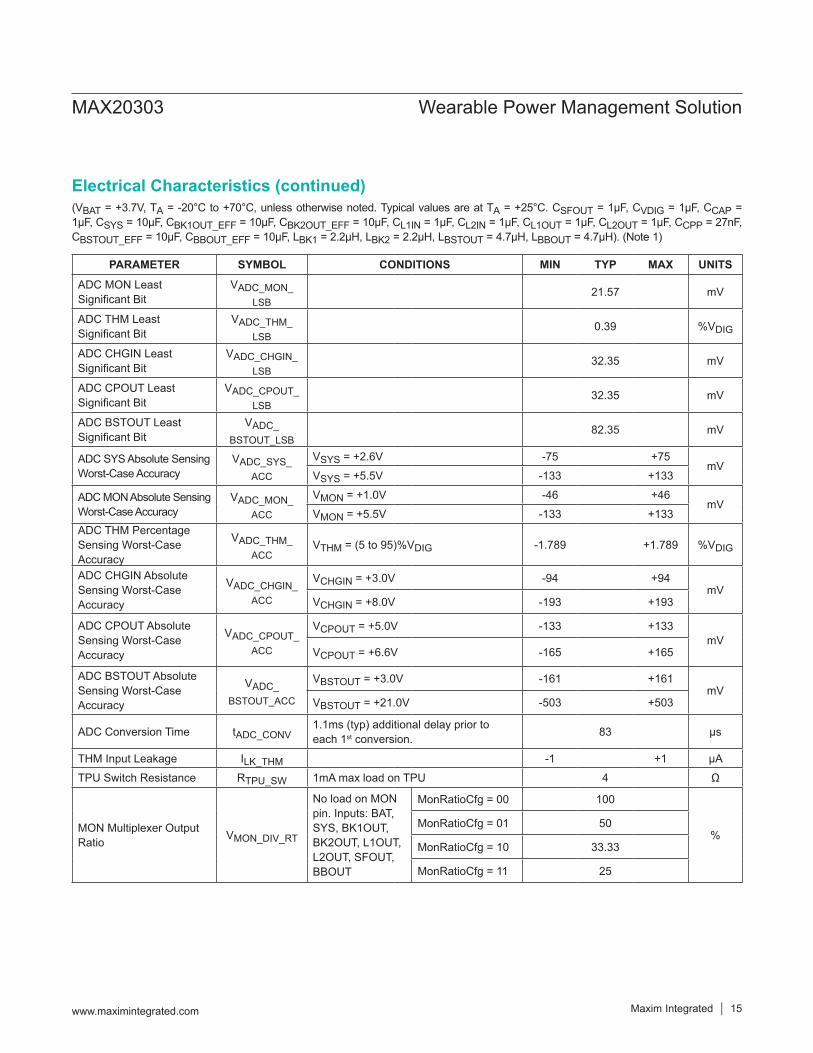
ADC MON Least Significant Bit
VADC_MON_ LSB
21.57 mV
ADC THM Least Significant Bit
VADC_THM_ LSB
0.39 %VDIG
ADC CHGIN Least Significant Bit
VADC_CHGIN_ LSB
32.35 mV
ADC CPOUT Least Significant Bit
VADC_CPOUT_LSB
32.35 mV
ADC BSTOUT Least Significant Bit
VADC_BSTOUT_LSB
82.35 mV
ADC SYS Absolute Sensing Worst-Case Accuracy
VADC_SYS_ ACC
VSYS = +2.6V -75 +75mV
VSYS = +5.5V -133 +133
ADC MON Absolute Sensing Worst-Case Accuracy
VADC_MON_ ACC
VMON = +1.0V -46 +46mV
VMON = +5.5V -133 +133ADC THM Percentage Sensing Worst-Case Accuracy
VADC_THM_ ACC
VTHM = (5 to 95)%VDIG -1.789 +1.789 %VDIG
ADC CHGIN Absolute Sensing Worst-Case Accuracy
VADC_CHGIN_ ACC
VCHGIN = +3.0V -94 +94mV
VCHGIN = +8.0V -193 +193
ADC CPOUT Absolute Sensing Worst-Case Accuracy
VADC_CPOUT_ACC
VCPOUT = +5.0V -133 +133mV
VCPOUT = +6.6V -165 +165
ADC BSTOUT Absolute Sensing Worst-Case Accuracy
VADC_BSTOUT_ACC
VBSTOUT = +3.0V -161 +161mV
VBSTOUT = +21.0V -503 +503
ADC Conversion Time tADC_CONV1.1ms (typ) additional delay prior to each 1st conversion. 83 µs
THM Input Leakage ILK_THM -1 +1 µA
TPU Switch Resistance RTPU_SW 1mA max load on TPU 4 Ω
MON Multiplexer Output Ratio VMON_DIV_RT
No load on MON pin. Inputs: BAT, SYS, BK1OUT, BK2OUT, L1OUT, L2OUT, SFOUT, BBOUT
MonRatioCfg = 00 100
%MonRatioCfg = 01 50
MonRatioCfg = 10 33.33
MonRatioCfg = 11 25
MAX20303 Wearable Power Management Solution
www.maximintegrated.com Maxim Integrated 15

(VBAT = +3.7V, TA = -20°C to +70°C, unless otherwise noted. Typical values are at TA = +25°C. CSFOUT = 1µF, CVDIG = 1µF, CCAP = 1µF, CSYS = 10µF, CBK1OUT_EFF = 10µF, CBK2OUT_EFF = 10µF, CL1IN = 1µF, CL2IN = 1µF, CL1OUT = 1µF, CL2OUT = 1µF, CCPP = 27nF, CBSTOUT_EFF = 10µF, CBBOUT_EFF = 10µF, LBK1 = 2.2µH, LBK2 = 2.2µH, LBSTOUT = 4.7µH, LBBOUT = 4.7µH). (Note 1)
Electrical Characteristics (continued)
PARAMETER SYMBOL CONDITIONS MIN TYP MAX UNITS
MON Multiplexer Output Impedance RMON_DIV
100µA load on MON pin. Inputs: BAT, SYS, BK2OUT, BK1OUT, L2OUT, L1OUT, SFOUT, BBOUT
MonRatioCfg = 00 5.5
kΩNo load on MON pin. Inputs: BAT, SYS, BK2OUT, BK1OUT, L2OUT, L1OUT, SFOUT, BBOUT
MonRatioCfg = 01 31
MonRatioCfg = 10 28
MonRatioCfg = 11 24
MON Multiplexer Off State Pulldown Resistance RMON_OFF_PD
MON disabled, pulldown resistance enabled 59 kΩ
OVP AND INPUT CURRENT LIMITERAllowed CHGIN Input Voltage Range VCHGIN_RNG -5.5 +28 V
CHGIN Overvoltage Rising Threshold VCHGIN_OV_R
SFOUT LDO is turned off above this threshold 7.2 7.5 7.8 V
CHGIN Overvoltage Threshold Hysteresis VCHGIN_OV_H 200 mV
CHGIN Valid Trip Point VCHGN-SYS_TP VCHGIN - VSYS 30 145 290 mV
CHGIN Valid Trip Point Hysteresis
VCHGIN-SYS_ TP-HYS
275 mV
Input Overcurrent Max Limit (t < tILIM_BLANK) ILIM_MAX
ILimMax = 0/1, device specific (see Table 192) 450/1000 mA
Input Current Limit (t > tILIM_BLANK) ILIM
ILimCnt = 000 50
mA
ILimCnt = 001 90
ILimCnt = 010 150
ILimCnt = 011 200
ILimCnt = 100 300
ILimCnt = 101 400
ILimCnt = 110 450
ILimCnt = 111 1000
MAX20303 Wearable Power Management Solution
www.maximintegrated.com Maxim Integrated 16

(VBAT = +3.7V, TA = -20°C to +70°C, unless otherwise noted. Typical values are at TA = +25°C. CSFOUT = 1µF, CVDIG = 1µF, CCAP = 1µF, CSYS = 10µF, CBK1OUT_EFF = 10µF, CBK2OUT_EFF = 10µF, CL1IN = 1µF, CL2IN = 1µF, CL1OUT = 1µF, CL2OUT = 1µF, CCPP = 27nF, CBSTOUT_EFF = 10µF, CBBOUT_EFF = 10µF, LBK1 = 2.2µH, LBK2 = 2.2µH, LBSTOUT = 4.7µH, LBBOUT = 4.7µH). (Note 1)
Electrical Characteristics (continued)
PARAMETER SYMBOL CONDITIONS MIN TYP MAX UNITS
Input Current Limit Blanking Time tILIM_BLANK
ILimBlank = 00 0.003
msILimBlank = 01 0.5
ILimBlank = 10 1
ILimBlank = 11 10
SYS Regulation Voltage VSYS_REG
VBAT_REG + 0.14
VBAT_REG +
0.2
VBAT_REG + 0.26
V
SYS Regulation Voltage Dropout VCHGIN-SYS 40 mV
CHGIN to SYS On-Resistance RCHGIN-SYS 0.37 0.66 Ω
Input Current Soft-Start Time ILIM_SFT 1 ms
Thermal Shutdown Temperature TCHGIN_SHDN
Future option
50
°C
60
70
80
90
100
110
MAX20303A,B,C,D 120
Thermal Shutdown Timeout
TCHGIN_SHDN_TO
TShdnTmo = 01 0.5
sTShdnTmo = 10 1
TShdnTmo = 11 5
BATTERY CHARGERBAT to SYS On Resistance RBAT-SYS
VBAT = 4.2V, IBAT = 300mA 80 140 mΩ
Thermal Regulation Temperature TCHG_LIM
TCHGIN_ SHDN - 3
°C
BAT-to-SYS Switch On Threshold VBAT-SYS_ON SYS falling 10 22 35 mV
BAT-to-SYS Switch Off Threshold VBAT-SYS_OFF SYS rising -3 -1.5 0 mV
SYS-BAT Charge Current Reduction Threshold VSYS-BAT_LIM
Measured as VSYS - VBAT, SysMinVlt = 000, VBAT > 3.6V 100 mV
MAX20303 Wearable Power Management Solution
www.maximintegrated.com Maxim Integrated 17

(VBAT = +3.7V, TA = -20°C to +70°C, unless otherwise noted. Typical values are at TA = +25°C. CSFOUT = 1µF, CVDIG = 1µF, CCAP = 1µF, CSYS = 10µF, CBK1OUT_EFF = 10µF, CBK2OUT_EFF = 10µF, CL1IN = 1µF, CL2IN = 1µF, CL1OUT = 1µF, CL2OUT = 1µF, CCPP = 27nF, CBSTOUT_EFF = 10µF, CBBOUT_EFF = 10µF, LBK1 = 2.2µH, LBK2 = 2.2µH, LBSTOUT = 4.7µH, LBBOUT = 4.7µH). (Note 1)
Electrical Characteristics (continued)
PARAMETER SYMBOL CONDITIONS MIN TYP MAX UNITS
Minimum SYS Voltage VSYS_LIM VBAT < 3.4V
SysMinVlt = 000 3.6
V
SysMinVlt = 001 3.7
SysMinVlt = 010 3.8
SysMinVlt = 011 3.9
SysMinVlt = 100 4.0
SysMinVlt = 101 4.1
SysMinVlt = 110 4.2
SysMinVlt = 111 4.3
Charger Current Soft-Start Time tCHG_SOFT 1 ms
Precharge Current IPCHG
IPChg = 00 5
%IFCHGIPChg = 01 9 10 11
IPChg = 10 20
IPChg = 11 30
Precharge Threshold VBAT_PCHG
VPChg = 000 2.1
V
VPChg = 001 2.25
VPChg = 010 2.4
VPChg = 011 2.55
VPChg = 100 2.7
VPChg = 101 2.85
VPChg = 110 3
VPChg = 111 3.15
Precharge Threshold Hysteresis
VBAT_PCHG_ HYS
90 mV
SET Current Gain Factor KSET 2000 A/A
SET Regulation Voltage VSET 1 V
BAT Charge Current Set Range IFCHG
RSET = 400kΩ 5
mARSET = 40kΩ 45 50 55
RSET = 4kΩ 500
MAX20303 Wearable Power Management Solution
www.maximintegrated.com Maxim Integrated 18

(VBAT = +3.7V, TA = -20°C to +70°C, unless otherwise noted. Typical values are at TA = +25°C. CSFOUT = 1µF, CVDIG = 1µF, CCAP = 1µF, CSYS = 10µF, CBK1OUT_EFF = 10µF, CBK2OUT_EFF = 10µF, CL1IN = 1µF, CL2IN = 1µF, CL1OUT = 1µF, CL2OUT = 1µF, CCPP = 27nF, CBSTOUT_EFF = 10µF, CBBOUT_EFF = 10µF, LBK1 = 2.2µH, LBK2 = 2.2µH, LBSTOUT = 4.7µH, LBBOUT = 4.7µH). (Note 1)
Electrical Characteristics (continued)
PARAMETER SYMBOL CONDITIONS MIN TYP MAX UNITS
Battery Regulation Voltage VBAT_REG
BatReg = 0000 4.05
V
BatReg = 0001 4.10
BatReg = 0010 4.15
BatReg = 0011, TA = 25°C 4.179 4.20 4.221
BatReg = 0011 4.158 4.20 4.242
BatReg = 0100 4.25
BatReg = 0101 4.30
BatReg = 0110 4.35
BatReg = 0111 4.40
BatReg = 1000 4.45
BatReg = 1001 4.50
BatReg = 1010 4.55
BatReg = 1011 4.60
Battery Recharge Threshold VBAT_RECHG
BatReChg = 00 70
mVBatReChg = 01 120
BatReChg = 10 170
BatReChg = 11 220
Maximum Precharge Time tPCHG
PChgTmr = 00 30
minPChgTmr = 01 60
PChgTmr = 10 120
PChgTmr = 11 240
Maximum Fast Charge Time tFCHG
FChgTmr = 00 75
minFChgTmr = 01 150
FChgTmr = 10 300
FChgTmr = 11 600
Charge Done Qualification ICHG_DONE
ChgDone = 00 5
%IFCHGChgDone = 01 8.5 10 11.5
ChgDone = 10 20
ChgDone = 11 30
Timer Accuracy tCHG_ACC -10 10 %
Timer Extend Threshold (1/2 Fast Charge Current Comparator)
tCHG_EXT See Figure 5 50 %IFCHG
MAX20303 Wearable Power Management Solution
www.maximintegrated.com Maxim Integrated 19

(VBAT = +3.7V, TA = -20°C to +70°C, unless otherwise noted. Typical values are at TA = +25°C. CSFOUT = 1µF, CVDIG = 1µF, CCAP = 1µF, CSYS = 10µF, CBK1OUT_EFF = 10µF, CBK2OUT_EFF = 10µF, CL1IN = 1µF, CL2IN = 1µF, CL1OUT = 1µF, CL2OUT = 1µF, CCPP = 27nF, CBSTOUT_EFF = 10µF, CBBOUT_EFF = 10µF, LBK1 = 2.2µH, LBK2 = 2.2µH, LBSTOUT = 4.7µH, LBBOUT = 4.7µH). (Note 1)
Electrical Characteristics (continued)
PARAMETER SYMBOL CONDITIONS MIN TYP MAX UNITS
Timer Suspend Threshold (1/5 Fast Charge Current Comparator)
tCHG_SUS See Figure 5 20 %IFCHG
THM Percentage Sensing Worst Case Accuracy
VADC_THM_ ACC
VTHM = (5 to 95)%VDIGsee ADC section
Cool/Cold Threshold Hysteresis Falling, LSB = 0.39%VDIG 0 to 31 LSB
Warm/Hot Threshold Hysteresis Rising, LSB = 0.39%VDIG 0 to 31 LSB
Battery Regulation Voltage Reduction Due to Battery Pack Temperature
VBAT_REG_ RED
Cold/Cool/Room/Warm/HotBatReg = 00
BatReg – 150mV
V
Cold/Cool/Room/Warm/HotBatReg = 01
BatReg – 100mV
Cold/Cool/Room/Warm/HotBatReg = 10
BatReg – 50mV
Cold/Cool/Room/Warm/HotBatReg = 11 BatReg
Fast Charge Current Reduction Due to Battery Pack Temperature
IFCHG_FACT
Cold/Cool/Room/Warm/HotFChg = 000
IFCHG x 0.2
mA
Cold/Cool/Room/Warm/HotFChg = 001
IFCHG x 0.3
Cold/Cool/Room/Warm/HotFChg = 010
IFCHG x 0.4
Cold/Cool/Room/Warm/HotFChg = 011
IFCHG x 0.5
Cold/Cool/Room/Warm/HotFChg = 100
IFCHG x 0.6
Cold/Cool/Room/Warm/HotFChg = 101
IFCHG x 0.7
Cold/Cool/Room/Warm/HotFChg = 110
IFCHG x 0.8
Cold/Cool/Room/Warm/HotFChg = 111 IFCHG
BAT UVLO Threshold VBAT_UVLO 1.9 2.05 2.2 V
BAT UVLO Threshold Hysteresis
VBAT_UVLO_ HYS
50 mV
MAX20303 Wearable Power Management Solution
www.maximintegrated.com Maxim Integrated 20

(VBAT = +3.7V, TA = -20°C to +70°C, unless otherwise noted. Typical values are at TA = +25°C. CSFOUT = 1µF, CVDIG = 1µF, CCAP = 1µF, CSYS = 10µF, CBK1OUT_EFF = 10µF, CBK2OUT_EFF = 10µF, CL1IN = 1µF, CL2IN = 1µF, CL1OUT = 1µF, CL2OUT = 1µF, CCPP = 27nF, CBSTOUT_EFF = 10µF, CBBOUT_EFF = 10µF, LBK1 = 2.2µH, LBK2 = 2.2µH, LBSTOUT = 4.7µH, LBBOUT = 4.7µH). (Note 1)
Electrical Characteristics (continued)
PARAMETER SYMBOL CONDITIONS MIN TYP MAX UNITSBUCK1Input Voltage Range VBK1IN Input voltage = VSYS 2.7 5.5 V
Output Voltage Range VBK1OUT 25mV step resolution 0.8 2.375 V
Output Voltage UVLO VUVLO_BK1 0.65 V
Quiescent Supply Current IQ_BK1IBK1OUT = 0, VSYS = +3.7V, VBK1OUT = +1.2V 0.8 1.3 µA
Dropout Quiescent Supply Current IQ_DO_BK1 IBK1OUT = 0, VSYS – VBK1OUT ≤ +0.1V 250 µA
Shutdown Supply Current with Active Discharge Enabled
ISD_BK1 Buck 1 disabled, Buck1ActDsc = 1 60 µA
Output Average Voltage Accuracy ACC_BK1 IBK1OUT = 1mA -3.2 +2.9 %
Peak-to-Peak Ripple VRPP_BK1
Buck1ISet = 0100 (100mA),CBK1OUT_EFF = 2.2µF, IBK1OUT = 1mA
10 mV
Peak Current Set Range IPSET_BK1
25mA step resolution. The accuracy of codes below 50mA is limited by tON_MIN_BK1
0 375 mA
Load Regulation Error VLOAD_REG_ BK1
Buck1ISet = 0110 (150mA),Buck1IAdptEn = 1, IBK1OUT = 300mA -3 %
Line Regulation Error VLINE_REG_ BK1
VBK1OUT = +1.2V, VSYS from +2.7V to +5.5V 2 mV
Maximum Operative Output Current IBK1_MAX
VSYS = +3.7V, Buck1VSet = 0x10 (+1.2V), Buck1ISet = 1000 (200mA), Buck1IAdptEn = 1, load regulation error = -5%
220 mA
BK1OUT Pulldown Current IPD_BK1_E Buck 1 Enabled 100 200 nA
BK1OUT Pulldown Resistance with Buck Disabled
IPD_BK1_DBuck 1 Disabled, VSYS = +3.6V, Buck1VSet = 0x10 (+1.2V) 12 MΩ
PMOS On-ResistanceRP_ON_BK1 Buck1FETScale = 0 0.35 0.49
ΩRP_ON_BK1_FS Buck1FETScale = 1 0.7 0.98
NMOS On-ResistanceRN_ON_BK1 Buck1FETScale = 0 0.25 0.4
ΩRN_ON_BK1_FS Buck1FETScale = 1 0.5 0.7
Freewheeling On-Resistance
RON_BK1_ FRWHL
VSYS = +3.7V,Buck1VSet = 0x10 (+1.2V) 7 12 Ω
MAX20303 Wearable Power Management Solution
www.maximintegrated.com Maxim Integrated 21

(VBAT = +3.7V, TA = -20°C to +70°C, unless otherwise noted. Typical values are at TA = +25°C. CSFOUT = 1µF, CVDIG = 1µF, CCAP = 1µF, CSYS = 10µF, CBK1OUT_EFF = 10µF, CBK2OUT_EFF = 10µF, CL1IN = 1µF, CL2IN = 1µF, CL1OUT = 1µF, CL2OUT = 1µF, CCPP = 27nF, CBSTOUT_EFF = 10µF, CBBOUT_EFF = 10µF, LBK1 = 2.2µH, LBK2 = 2.2µH, LBSTOUT = 4.7µH, LBBOUT = 4.7µH). (Note 1)
Electrical Characteristics (continued)
PARAMETER SYMBOL CONDITIONS MIN TYP MAX UNITS
Minimum tON tON_MIN_BK1 60 90 ns
Maximum Duty Cycle D_MAX_BK1 Buck1IAdptEn = 1 95 %
Switching Frequency FREQ_BK1 Load regulation error = -5% 3 MHz
Average Current During Short-Circuit to GND ISHRT_BK1
Buck1ISet = 0110 (150mA), Buck1IAdptEn = 1, VBK1OUT = 0V 100 mA
BK1LX Leakage Current ILK_BK1LX Buck 1 disabled 1 µA
Active Discharge Current IACTD_BK1 VBK1OUT = +1.2V 8 19 35 mA
Passive Discharge Resistance RPSV_BK1 10 kΩ
Full Turn-On Time tON_BK1Time from enable to full current capability 58 ms
Efficiency EFFIC_BK1Buck1VSet = 0x10 (+1.2V), IBK1OUT = 10mA, Buck1ISet = 0111 (175mA), Inductor: Murata DFE201610E-2R2M
88.5 %
BK1LX Rising/Falling Slew Rate
SLW_BK1 Buck1LowEMI = 0 2V/ns
SLW_BK1_L Buck1LowEMI = 1 0.5
Thermal Shutdown Threshold TSHDN_BK1 140 °C
BUCK2Input Voltage Range VBK2IN Input voltage = VSYS 2.7 5.5 V
Output Voltage Range VBK2OUT 50mV step resolution 0.8 3.95 V
Output Voltage UVLO VUVLO_BK2 0.65 V
Quiescent Supply Current IQ_BK2IBK2OUT = 0mA, VSYS = +3.7V,Buck2VSet = 0x08 (+1.2V) 0.9 1.4 µA
Dropout Quiescent Supply Current IQ_DO_BK2
IBK2OUT = 0mA, VSYS – VBK2OUT ≤ +0.1V 250 µA
Shutdown Supply Current with Active Discharge Enabled
ISD_BK2 Buck 2 disabled, Buck2ActDsc = 1 60 µA
Output Average Voltage Accuracy ACC_BK2 IBK2OUT = 1mA, Buck2VSet ≤ 0x34
(+3.4V) -3.2 +2.9 %
Peak-to-Peak Ripple VRPP_BK2Buck2ISet = 0100 (100mA),CBK2OUT_EFF = 2.2µF, IBK2OUT = 1mA 10 mV
Peak Current Set Range IPSET_BK2
25mA step resolution. The accuracy of codes below 50mA is limited by tON_MIN_BK2
0 375 mA
MAX20303 Wearable Power Management Solution
www.maximintegrated.com Maxim Integrated 22

(VBAT = +3.7V, TA = -20°C to +70°C, unless otherwise noted. Typical values are at TA = +25°C. CSFOUT = 1µF, CVDIG = 1µF, CCAP = 1µF, CSYS = 10µF, CBK1OUT_EFF = 10µF, CBK2OUT_EFF = 10µF, CL1IN = 1µF, CL2IN = 1µF, CL1OUT = 1µF, CL2OUT = 1µF, CCPP = 27nF, CBSTOUT_EFF = 10µF, CBBOUT_EFF = 10µF, LBK1 = 2.2µH, LBK2 = 2.2µH, LBSTOUT = 4.7µH, LBBOUT = 4.7µH). (Note 1)
Electrical Characteristics (continued)
PARAMETER SYMBOL CONDITIONS MIN TYP MAX UNITS
Load Regulation Error VLOAD_REG_ BK2
Buck2ISet = 0110 (150mA),Buck2IAdptEn = 1, IBK2OUT = 300mA -3 %
Line Regulation Error VLINE_REG_ BK2
VBK2OUT = +1.2V, VSYS from +2.7V to +5.5V 2 mV
Maximum Operative Output Current IBK2_MAX
VSYS = +3.7V, Buck2VSet = 0x08 (+1.2V), Buck2ISet = 1000 (200mA), Buck2IAdptEn = 1, load regulation error = -5%
220 mA
BK2OUT Pulldown Current IPD_BK2_E Buck 2 enabled 200 400 nA
BK2OUT Pulldown Resistance with Buck Disabled
IPD_BK2_DBuck 2 disabled, VSYS = +3.6V, Buck2VSet = 0x10 (+1.2V) 8 MΩ
PMOS On-ResistanceRP_ON_BK2 Buck2FETScale = 0 0.35 0.49
ΩRP_ON_BK2_FS Buck2FETScale = 1 0.7 0.98
NMOS On-ResistanceRN_ON_BK2 Buck2FETScale = 0 0.25 0.4
ΩRN_ON_BK2_FS Buck2FETScale = 1 0.5 0.7
Freewheeling On-Resistance
RON_BK2_ FRWHL
VSYS = +3.7V,Buck2VSet = 0x08 (+1.2V) 7 12 Ω
Minimum tON tON_MIN_BK2 60 90 ns
Maximum Duty Cycle D_MAX_BK2 Buck2IAdptEn = 1 95 %
Switching Frequency FREQ_BK2 Load regulation error = -5% 3 MHz
Average Current During Short-Circuit to GND ISHRT_BK2
Buck2ISet = 0110 (150mA), Buck2IAdptEn = 1, VBK2OUT = 0V 100 mA
BK2LX Leakage Current ILK_BK2LX Buck 2 disabled 1 µA
Active Discharge Current IACTD_BK2 VBK2OUT = +1.2V 8 19 35 mA
Passive Discharge Resistance RPSV_BK2 10 kΩ
Full Turn-On Time tON_BUCK2Time from enable to full current capability 58 ms
Efficiency EFFIC_BK2Buck2VSet = 0x08 (+1.2V), IBK2OUT = 10mA, Buck2ISet = 0111 (175mA), Inductor: Murata DFE201610E-2R2M
88.5 %
BK2LX Rising/Falling Slew Rate
SLW_BK2 Buck2LowEMI = 0 2V/ns
SLW_BK2_L Buck2LowEMI = 1 0.5
Thermal Shutdown Threshold TSHDN_BK2 140 °C
MAX20303 Wearable Power Management Solution
www.maximintegrated.com Maxim Integrated 23

(VBAT = +3.7V, TA = -20°C to +70°C, unless otherwise noted. Typical values are at TA = +25°C. CSFOUT = 1µF, CVDIG = 1µF, CCAP = 1µF, CSYS = 10µF, CBK1OUT_EFF = 10µF, CBK2OUT_EFF = 10µF, CL1IN = 1µF, CL2IN = 1µF, CL1OUT = 1µF, CL2OUT = 1µF, CCPP = 27nF, CBSTOUT_EFF = 10µF, CBBOUT_EFF = 10µF, LBK1 = 2.2µH, LBK2 = 2.2µH, LBSTOUT = 4.7µH, LBBOUT = 4.7µH). (Note 1)
Electrical Characteristics (continued)
PARAMETER SYMBOL CONDITIONS MIN TYP MAX UNITSHVBOOSTInput Voltage Range VBSTIN Input voltage = VSYS 2.7 5.5 V
Output Voltage Range VBSTOUT 250mV step resolution 5 20 V
Output Voltage UVLO VBSTOUT_ UVLO
VBSTOUT - VSYS -2.7 -2.2 -1.6 V
Quiescent Supply Current IQ_BST
IBSTOUT = 0mA, VSYS = +3.7V,BstVSet = 0x00 (+5V), TA = 25°C 2.4 9
µAIBSTOUT = 0mA, VSYS = +3.7V,BstVSet = 0x00 (+5V) 106
Output Average Voltage Accuracy ACC_BST IBSTOUT = 1mA, HVOUT < 13V -4 +2 %
Peak-to-Peak Ripple VRPP_BST
BstISet = 0x0A (350mA),BstVSet = 0x1C (+12V),CBSTOUT_EFF = 10µF, L = 4.7µH, IBSTOUT = 1mA
5 mV
Peak Current Set Range IPSET_BST 25mA step resolution 100 475 mA
DC Load Regulation Error VLOAD_REG_ BST
BstVSet = 0x1C (+12V), IBSTOUT = 25mA, BstISet = 0x08 (300mA),BstIAdptEn = 1
0.3 %
DC Line Regulation Error VLINE_REG_ BST
BstVSet = 0x06 (+6.5V), VSYS from +2.7V to +5.5V 4 mV
Maximum Operative Output Power PMAX_BST
BstISet = 0x08 (300mA),BstIAdptEn = 1 300 700 mW
BSTOUT Pulldown Resistance RBSTOUT -3% Load Reg Error 10 MΩ
True Shutdown PMOS On-Resistance RON_TS IBSTOUT = 100mA 0.15 0.22 Ω
Boost Freewheeling NMOS On-Resistance RN_ONFRW_N IBSTOUT = 100mA 0.45 0.7 Ω
Boost NMOS On-Resistance
RONBST_N BstFETScale = 0, IBSTOUT = 100mA 0.55 0.9Ω
RONBST_NFS BstFETScale = 1, IBSTOUT = 100mA 1.1 1.8
Schottky Diode Forward Voltage
VBE_ SCHOTTKY
IBSTOUT = 100mA, VBSTHVLX - VBSTOUT
0.2 0.4 0.6 V
Freewheeling On-Resistance
RONBST_ FRWHL
IBSTOUT = 100mA 50 80 Ω
Minimum tON tON_BST_MIN 65 ns
MAX20303 Wearable Power Management Solution
www.maximintegrated.com Maxim Integrated 24

(VBAT = +3.7V, TA = -20°C to +70°C, unless otherwise noted. Typical values are at TA = +25°C. CSFOUT = 1µF, CVDIG = 1µF, CCAP = 1µF, CSYS = 10µF, CBK1OUT_EFF = 10µF, CBK2OUT_EFF = 10µF, CL1IN = 1µF, CL2IN = 1µF, CL1OUT = 1µF, CL2OUT = 1µF, CCPP = 27nF, CBSTOUT_EFF = 10µF, CBBOUT_EFF = 10µF, LBK1 = 2.2µH, LBK2 = 2.2µH, LBSTOUT = 4.7µH, LBBOUT = 4.7µH). (Note 1)
Electrical Characteristics (continued)
PARAMETER SYMBOL CONDITIONS MIN TYP MAX UNITS
Max Switching Frequency FREQ_BST_ MX
VBSTOUT regulation error = -150mV. BstISet = 100mA, BstIAdptEn = 0. 1.7 3.5 5.5 MHz
Max Peak Current Setting Extra Budget with BstIAdptEn = 1
ΔIP_MAXBstIAdptEn = 1, VBSTOUT regulation error = -200mV 150 250 450 mA
Short-Circuit Current Limit Difference vs. Peak Current Setting
ΔIBST_SHRT BstIAdptEn = 0 130 200 250 mA
BSTHVLX Leakage Current ILK_BSTHVLX Boost disabled 1 µA
BSTLVLX Leakage Current ILK_BSTLVLX Boost disabled 1 µA
Passive Discharge Resistance RBSTPSV 10 kΩ
Linear BSTOUT Precharge Current
IL_BSTOUT_ PRCH
VBSTOUT from 0 to VSYS – 0.4V 5 12.5 20 mA
Switching Precharge Inductor Current
ISW_BSTOUT_ PRCH
VBSTOUT from VSYS – 0.4V to final regulation voltage 13 mA
Full Turn-On Time tON_BSTTime from enable to full current capability 100 ms
Efficiency
EFFIC_12BstVSet = 0x1C (+12V), IBSTOUT = 20mA, BstISet = 0x08 (300mA), Inductor: Murata DFE201610E-4R7M
85
%
EFFIC_15BstVSet = 0x28 (+15V), IBSTOUT = 2mA, BstISet = 0x08 (300mA), Inductor: Murata DFE201610E-4R7M
83
EFFIC_5BstVSet = 0x00 (+5V), IBSTOUT = 10µA, BstISet = 0x02 (150mA), Inductor: Murata DFE201610E-4R7M
76
EFFIC_6P5BstVSet = 0x06 (+6.5V), IBSTOUT = 10µA, BstISet = 0x02 (150mA), Inductor: Murata DFE201610E-4R7M
73
BHVLX Rising/Falling Slew Rate
SLW_BST HVLX 2 V/ns
Thermal Shutdown Threshold TSHDN_BST 125 °C
MAX20303 Wearable Power Management Solution
www.maximintegrated.com Maxim Integrated 25

(VBAT = +3.7V, TA = -20°C to +70°C, unless otherwise noted. Typical values are at TA = +25°C. CSFOUT = 1µF, CVDIG = 1µF, CCAP = 1µF, CSYS = 10µF, CBK1OUT_EFF = 10µF, CBK2OUT_EFF = 10µF, CL1IN = 1µF, CL2IN = 1µF, CL1OUT = 1µF, CL2OUT = 1µF, CCPP = 27nF, CBSTOUT_EFF = 10µF, CBBOUT_EFF = 10µF, LBK1 = 2.2µH, LBK2 = 2.2µH, LBSTOUT = 4.7µH, LBBOUT = 4.7µH). (Note 1)
Electrical Characteristics (continued)
PARAMETER SYMBOL CONDITIONS MIN TYP MAX UNITSBUCK-BOOSTInput Voltage Range VBBIN Input voltage = VSYS 2.7 5.5 V
Quiescent Supply Current IQ_BB IBBOUT = 0µA, VBBOUT = +4V 1.3 2.1 µA
Maximum Output Operative Power PMAX_BBOUT VSYS > +3V 250 mW
Output Voltage Set Range VBBOUT 100mV step 2.5 5 V
Average Output Voltage Accuracy ACC_BBOUT IBBOUT = 1mA, CBBOUT_EFF ≥ 10µF -3 3 %
Line Regulation Error VLINE_REG_ BB
VSYS = +2.7V to +5.5V, IBBOUT = 10µA, BBstVSet = 0x0F (+4V), BBstISet = 0x02 (100mA)
-1 +0.3 +1 %/V
Load Regulation Error VLOAD_REG_ BB
BBstVSet = 0x0F (+4V), IBBOUT = 10µA to 50mA, BBstISet = 0x02 (100mA) 100
mV/ABBstVSet = 0x0F (+4V), IBBOUT = 10µA to 100mA, BBstISet = 0x02 (100mA) 310
Line Transient VLINE_TRAN_ BB
BBstVSet = 0x0F (+4V), BBstISet = 0x02 (100mA), VSYS from +2.7V to +5V, 0.2µs rise time
15 mV
Load Transient VLOAD_ TRAN_BB
IBBOUT = 0mA to 10mA, 200ns rise time, BBstVSet = 0x0F (+4V), BBstISet = 0x02 (100mA)
9
mVIBBOUT = 0mA to 100mA, 200ns rise time, VBBOUT = +4V, BBstISet = 0x02 (100mA)
31
Oscillator Frequency fOSC_BB 1.8 2 2.2 MHz
Output FETs RON
RON_PBK_BB High-side PMOS Buck FET 0.15 0.22
Ω
RON_NBK_BB Low-side NMOS Buck FET 0.22 0.36
RON_PBST_BBHigh-side PMOS Boost FET (VBBOUT = +4V) 0.21 0.31
RON_NBST_BB Low-side NMOS Boost FET 0.24 0.4
RON_FRWH_BBEMI improve FET between BBHVLX/BBLVLX 8 11
Passive Discharge Pulldown Resistance RPDL_BB BBstPasDsc = 1 10 kΩ
Active Discharge Current IACTDL_BB BBstActDsc = 1, VBBOUT = +1.5V 6 19 38 mA
MAX20303 Wearable Power Management Solution
www.maximintegrated.com Maxim Integrated 26

(VBAT = +3.7V, TA = -20°C to +70°C, unless otherwise noted. Typical values are at TA = +25°C. CSFOUT = 1µF, CVDIG = 1µF, CCAP = 1µF, CSYS = 10µF, CBK1OUT_EFF = 10µF, CBK2OUT_EFF = 10µF, CL1IN = 1µF, CL2IN = 1µF, CL1OUT = 1µF, CL2OUT = 1µF, CCPP = 27nF, CBSTOUT_EFF = 10µF, CBBOUT_EFF = 10µF, LBK1 = 2.2µH, LBK2 = 2.2µH, LBSTOUT = 4.7µH, LBBOUT = 4.7µH). (Note 1)
Electrical Characteristics (continued)
PARAMETER SYMBOL CONDITIONS MIN TYP MAX UNITS
Turn-On Time tON_BBTime from enable to full current capability 100 ms
UVLO On BBOUT VBBOUT_UVLO 1.65 1.75 1.9 V
Precharge Current IPC_BBPrecharge current. VSYS = +2.7V, VBBOUT = +1.65V 6 14 24 mA
Pulse Mode Input Current Limit IPLS_IN
BBstVSet = 0x0F (+4V), VSYS < VBBOUT – 0.5V, fSW = fOSC_BBST/10, BBstISet = 0x02 (100mA)
6.6 mA
Pulse Mode Switching Period Ratio T_RATIO fOSC_BB/fSW 128 steps 10 138
Average Current During Short-Circuit to GND ISHRT_BB VBBOUT = 0V 0.4 0.75 1.1 A
Thermal Shutdown Threshold TSHDN_BB TJ rising 150 °C
Thermal Shutdown Hysteresis
TSHDN_ HYST_BB
10 °C
LDO1 (Typical values are at VL1IN = +1.2V, VL1OUT = +1V)
Input Voltage Range VL1INLDO mode 1.16 2
VSwitch mode 0.7 2
Quiescent Supply Current IQ_L1IL1OUT = 0µA 1 2.1
µAIL1OUT = 0µA, Switch mode 0.35 0.7
Output Leakage ILK_L1OUT VL1OUT = GND, LDO 1 disabled 0.015 2.5 µA
Quiescent Supply Current in Dropout IQ_L1_DRP
IL1OUT = 0µA, VL1IN = +1.2V, LDO1VSet = 0x1D (+1.225V) 2.4 4.2 µA
Maximum Output Current IL1OUT_MAX 50 mA
Output Voltage VL1OUT 25mV step resolution 0.5 1.95 V
Output Accuracy ACC_LDO1 (VL1OUT + 0.2V) ≤ VL1IN ≤ +2V, IL1OUT = 1mA -3.4 +3.9 %
Dropout Voltage VDRP_L1VL1IN = +1V, LDO1VSet = 0x14 (+1V), IL1OUT = 50mA 63 mV
Line Regulation Error VLINE_REG_L1 VL1IN = (VL1OUT + 0.2V) to +2V -0.5 +0.5 %/V
Load Regulation Error VLOAD_REG_L1+1V ≤ VL1IN ≤ +2V ,IL1OUT = 100µA to 50mA 0.003 0.013 %/mA
Line Transient VLINE_TRAN_ L1
VL1IN = +1V to +2V, 200ns rise time ±45mV
VL1IN = +1V to +2V, 1µs rise time ±25
Load Transient VLOAD_TRAN_ L1
IL1OUT = 0 to 10mA, 200ns rise time 80mV
IL1OUT = 0 to 50mA, 200ns rise time 130
MAX20303 Wearable Power Management Solution
www.maximintegrated.com Maxim Integrated 27

(VBAT = +3.7V, TA = -20°C to +70°C, unless otherwise noted. Typical values are at TA = +25°C. CSFOUT = 1µF, CVDIG = 1µF, CCAP = 1µF, CSYS = 10µF, CBK1OUT_EFF = 10µF, CBK2OUT_EFF = 10µF, CL1IN = 1µF, CL2IN = 1µF, CL1OUT = 1µF, CL2OUT = 1µF, CCPP = 27nF, CBSTOUT_EFF = 10µF, CBBOUT_EFF = 10µF, LBK1 = 2.2µH, LBK2 = 2.2µH, LBSTOUT = 4.7µH, LBBOUT = 4.7µH). (Note 1)
Electrical Characteristics (continued)
PARAMETER SYMBOL CONDITIONS MIN TYP MAX UNITS
Passive Discharge Resistance RPDL_L1 5 10 15 kΩ
Active Discharge Current IACTDL_L1 7 25 55 mA
Switch Mode On-Resistance RON_L1 Switch mode
VL1IN = +1V, IL1OUT = 50mA 1.02
ΩVL1IN = +0.7V, IL1OUT= 1mA 2.7
Turn-On Time tON_L1
IL1OUT = 0mA, time from 10% to 90% of LDO1VSet 0.38
msIL1OUT = 0mA, time from 10% to 90% of VL1IN, Switch mode 0.065
Short Circuit Current Limit ISHRT_L1
VL1IN = +1.2V, VL1OUT = 0V 165 310 405mAVL1IN = +1.2V, VL1OUT = 0V, Switch
mode 160 305 400
Thermal Shutdown Temperature TSHDN_L1 TJ rising 150 °C
Thermal Shutdown Temperature Hysteresis
TSHDN_ HYS_L1
20 °C
Output Noise 10Hz to 100kHz, VL1IN = +2V
VL1OUT = +1.8V 120
µVRMSVL1OUT = +1V 95
VL1OUT = +0.5V 70
UVLOVL1IN_UVLO_F VL1IN falling 0.53 0.77
VVL1IN_UVLO_R VL1IN rising 0.78 1
LDO2 (Typical values at VL2IN = +3.7V, VL2OUT = +3V)
Input Voltage Range VL2INLDO mode 1.71 5.5
VSwitch mode 1.2 5.5
Quiescent Supply Current IQ_L2IL2OUT = 0µA 1 1.7
µAIL2OUT = 0µA, Switch mode. 0.35 0.7
Quiescent Supply Current in Dropout IQ_L2_DRP
IL2OUT = 0µA, VL2IN = +2.9V, LDO2VSet = 0x15 (+3V) 2.2 3.7 µA
Maximum Output Current IL2OUT_MAX VL2IN > +1.8V 100 mA
Output Voltage VL2OUT 100mV step resolution 0.9 4 V
Output Accuracy ACC_LDO2 (VL2OUT + 0.5V) ≤ VL2IN ≤ +5.5V, IL2OUT = 1mA -2.9 +2.9 %
Dropout Voltage VDRP_L2
VL2IN = +3V, LDO2VSet = 0x16 (+3.1V), IL2OUT = 100mA 100 mV
VL2IN = +1.85V, LDO2VSet = 0x0A (+1.9V), IL2OUT = 100mA 130 mV
MAX20303 Wearable Power Management Solution
www.maximintegrated.com Maxim Integrated 28

(VBAT = +3.7V, TA = -20°C to +70°C, unless otherwise noted. Typical values are at TA = +25°C. CSFOUT = 1µF, CVDIG = 1µF, CCAP = 1µF, CSYS = 10µF, CBK1OUT_EFF = 10µF, CBK2OUT_EFF = 10µF, CL1IN = 1µF, CL2IN = 1µF, CL1OUT = 1µF, CL2OUT = 1µF, CCPP = 27nF, CBSTOUT_EFF = 10µF, CBBOUT_EFF = 10µF, LBK1 = 2.2µH, LBK2 = 2.2µH, LBSTOUT = 4.7µH, LBBOUT = 4.7µH). (Note 1)
Electrical Characteristics (continued)
PARAMETER SYMBOL CONDITIONS MIN TYP MAX UNITSLine Regulation Error VLINE_REG_L2 VL2IN = (VL2OUT + 0.5V) to +5.5V -0.38 +0.38 %/V
Load Regulation Error VLOAD_REG_ L2
+1.8V ≤ VL2IN ≤ +5.5VIL2OUT = 100µA to 100mA 0.002 0.005 %/mA
Line Transient VLINE_TRAN_ L2
VL2IN = +4V to +5V, 200ns rise time ±35mV
VL2IN = +4V to +5V, 1µs rise time ±25
Load Transient VLOAD_TRAN_ L2
IL2OUT = 0mA to 10mA, 200ns rise time 100
mVIL2OUT = 0mA to 100mA, 200ns rise time 200
Passive Discharge Resistance RPDL_L2 5 10 15 kΩ
Active Discharge Current IACTDL_L2 8 22 40 mA
Switch Mode On-Resistance RON_L2 Switch mode
VL2IN = +2.7V, IL2OUT = 100mA 0.7
ΩVL2IN = +1.8V, IL2OUT = 50mA 1
VL2IN = +1.2V, IL2OUT = 5mA 2.3
Turn-On Time tON_L2
IL2OUT = 0mA, time from 10% to 90% of LDO2VSet 1.5
msIL2OUT = 0mA, time from 10% to 90% of VL2IN. Switch mode 0.26
Short Circuit Current Limit ISHRT_L2
VL2IN = +2.7V, VL2OUT = 0V 225 360 555mAVL2IN = +2.7V, VL2OUT = 0V,
Switch mode 210 350 540
Thermal Shutdown Temperature TSHDN_L2 TJ rising 150 °C
Thermal Shutdown Temperature Hysteresis TSHDN_HYS_L2 20 °C
Output Noise10Hz to 100kHz, VL2IN = +5V
VL2OUT = +3.3V 150
µVRMSVL2OUT = +2.5V 125
VL2OUT = +1.2V 90
VL2OUT = +0.9V 80
UVLO VL2IN_UVLOVL2IN falling 1.05 1.35
VVL2IN rising 1.36 1.69
MAX20303 Wearable Power Management Solution
www.maximintegrated.com Maxim Integrated 29

(VBAT = +3.7V, TA = -20°C to +70°C, unless otherwise noted. Typical values are at TA = +25°C. CSFOUT = 1µF, CVDIG = 1µF, CCAP = 1µF, CSYS = 10µF, CBK1OUT_EFF = 10µF, CBK2OUT_EFF = 10µF, CL1IN = 1µF, CL2IN = 1µF, CL1OUT = 1µF, CL2OUT = 1µF, CCPP = 27nF, CBSTOUT_EFF = 10µF, CBBOUT_EFF = 10µF, LBK1 = 2.2µH, LBK2 = 2.2µH, LBSTOUT = 4.7µH, LBBOUT = 4.7µH). (Note 1)
Electrical Characteristics (continued)
PARAMETER SYMBOL CONDITIONS MIN TYP MAX UNITSCHARGE PUMPInput Voltage VCPIN Input voltage = VSYS 2.7 5.5 V
Quiescent Supply CurrentIQ_CP_5V ICPOUT = 0µA, CPVSet = 1 (+5V) 2 3.5
µAIQ_CP_6.6V ICPOUT = 0µA, CPVSet = 0 (+6.6V) 2.2 4.3
CPOUT Output Voltage VCPOUT
CPVSet = 0, ICPOUT = 10µA, VSYS > +3.3V 6.6
VCPVSet = 1, ICPOUT = 10µA 5
Output Accuracy ACC_CP ICPOUT < 120µA, VSYS > +3.3V -3 +3 %
Maximum Operative Output Current ICPOUT_MAX
VSYS > +3.3V, -5% load regulation error 250 µA
Efficiency EFF_CP CPVSet = 0 (+6.6V), IOUT = 10µA, VSYS = +3.7V 79 %
Max Charge Pump Frequency FREQ_CP 88 100 110 kHz
Passive Discharge Resistance RPSV_CP 10 kΩ
HAPTIC DRIVERInput Voltage VHD_IN Input voltage = VSYS 2.6 5.5 V
Quiescent Current IHD_Q VDRP/VDRN = 0 to VSYS 1300 µA
H-Bridge PWM Output Frequency fHD_PWM_OUT 22.5 25 27.5 kHz
H-Bridge PWM Output Duty Cycle Resolution
DHD_PWM_ OUT
7 bits VSYS/ 128 %VSYS
H-Bridge Output Impedance in Off State RHD_OFF
HptOffImp = 1 15 kΩ
HptOffImp = 0 RHD_ON_LS Ω
H-Bridge Output Leakage in High-Z State IHD_LK_OUT
During back EMF detection, VDRP/VDRN = 0 to VSYS
-1 +1 µA
H-Bridge On-ResistanceRHD_ON_HS
High-side PMOS switch on, 300mA load 0.04 0.18 0.5
ΩRHD_ON_LS
Low-side NMOS switch on, 300mA load 0.04 0.18 0.5
H-Bridge Overcurrent Protection Threshold IHD_OC_THR
Rising current through high-side or low-side 600 1000 1500 mA
H-Bridge Overcurrent Protection Hysteresis IHD_OC_HYS 130 mA
MAX20303 Wearable Power Management Solution
www.maximintegrated.com Maxim Integrated 30

(VBAT = +3.7V, TA = -20°C to +70°C, unless otherwise noted. Typical values are at TA = +25°C. CSFOUT = 1µF, CVDIG = 1µF, CCAP = 1µF, CSYS = 10µF, CBK1OUT_EFF = 10µF, CBK2OUT_EFF = 10µF, CL1IN = 1µF, CL2IN = 1µF, CL1OUT = 1µF, CL2OUT = 1µF, CCPP = 27nF, CBSTOUT_EFF = 10µF, CBBOUT_EFF = 10µF, LBK1 = 2.2µH, LBK2 = 2.2µH, LBSTOUT = 4.7µH, LBBOUT = 4.7µH). (Note 1)
Electrical Characteristics (continued)
PARAMETER SYMBOL CONDITIONS MIN TYP MAX UNITS
H-Bridge Thermal Shutdown Temperature Threshold
THD_SHDN_ THR
Rising temperature 150 °C
H-Bridge Thermal Shutdown Temperature Hysteresis
THD_SHDN_ HYS
25 °C
PWM Input Frequency fHD_INPWM 10 250 kHz
LRA Resonance Frequency Tracking Range
fHD_LRA See Haptic Driver section 120 305 Hz
Startup Latency tHD_STARTTime from command to vibration response. See Haptic Driver section 10 12 ms
LED CURRENT SINKSMaximum Input Voltage VIN_LED_MAX 20 V
Quiescent Current IQ_LED All LEDs on, VSYS = 3.7V 245 370 µA
Current Sink Setting Range ILED_RNG
LEDIStep = 00 (0.6mA steps) 0.6 15
mALEDIStep = 01 (1mA steps) 1 25
LEDIStep = 10 (1.2mA steps) 1.2 30
LED Current Accuracy ACC_LED
ILED_ = 13mA, TA = +25°C, VLED_ = +0.7V to +20V -2 +2
%ILED_ = 13mA, VLED_ = +0.7V to +20V -4 +4
ILED_ = 0.6mA to 30mA, VLED_ = +0.7V to +20V, TA = 25°C -5 +5 %
ILED_ = 0.6mA to 30mA, VLED_ = +0.7V to +20V -6 +6 %
LED Dropout Voltage VLED_DROP
ILED_SET = 5mA, ILED_= 0.9 x 5mA 110 160
mVILED_SET = 25mA, ILED_ = 0.9 x 25mA 145 215
ILED_SET = 30mA, ILED_ = 0.9 x 30mA 175 270
Leakage in Shutdown ILK_LED VLED_ = +20V 0.1 µA
Open-LED Detection Threshold VLED_DET
LED_ enabled, LEDIStep = 00, falling edge 61 92 140 mV
MAX20303 Wearable Power Management Solution
www.maximintegrated.com Maxim Integrated 31

(VBAT = +3.7V, TA = -20°C to +70°C, unless otherwise noted. Typical values are at TA = +25°C. CSFOUT = 1µF, CVDIG = 1µF, CCAP = 1µF, CSYS = 10µF, CBK1OUT_EFF = 10µF, CBK2OUT_EFF = 10µF, CL1IN = 1µF, CL2IN = 1µF, CL1OUT = 1µF, CL2OUT = 1µF, CCPP = 27nF, CBSTOUT_EFF = 10µF, CBBOUT_EFF = 10µF, LBK1 = 2.2µH, LBK2 = 2.2µH, LBSTOUT = 4.7µH, LBBOUT = 4.7µH). (Note 1)
Electrical Characteristics (continued)
PARAMETER SYMBOL CONDITIONS MIN TYP MAX UNITS
FUEL GUAGE
Supply Voltage VCELL (Note 3) 2.5 4.5 V
Fuel-Gauge SOC Reset (VRESET Register) VRST
Configuration range, in 40mV steps 2.28 3.48V
Trimmed at 3V 2.85 3.0 3.15
Supply CurrentIDD0
Sleep mode 0.5 2
µA
Hibernate mode, reset comparator disabled (VRESET.Dis = 1) 3 5
Hibernate mode, reset comparator enabled (VRESET.Dis = 0) 4 6
IDD1 Active mode 23 40
Time Base Accuracy tERR Active, hibernate modes (Note 4) -3.5 +3.5 %
AD Sample PeriodActive mode 250 msHibernate mode 45 s
Voltage Error VERRVCELL = 3.6V, TA = +25°C (Note 5) -9 +6
mV/cellTA = -20°C to +70°C -23 +20
Votlage-Measurement Resolution 1.25 mV/cell
BAT-to-Cell On-Resistance RON_ISO VBAT = 3.7V 15 30 Ω
Bus Low-Detection Timeout tSLEEP (Notes 6, 7) 2.125 sDIGITAL
SDA, SCL, MPC_, PFN_ Input Leakage Current
ILK_IOInput pullup/pulldown resistances disabled, input voltage from 0 to +5.5V -1 +1 µA
SDA, SCL, MPC_ Input Logic-High VIO_IH 1.4 V
SDA, SCL, MPC_ Input Logic-Low VIO_IL 0.5 V
PFN_ Input Logic-High VPFN_IH (Note 2) 0.7 x VCCINT
V
PFN_ Input Logic-Low VPFN_IL (Note 2) 0.3 x VCCINT
V
MPC_, PFN_ Input Pullup Resistance RIO_UP Pullup resistance to VCCINT (Note 2) 170 kΩ
MPC_, PFN_ Input Pulldown Resistance RIO_PD 170 kΩ
MPC_ Output Logic-High VIO_OHIOH = 1mA, MPC_ configured as push-pull output, pullup voltage is VBK2OUT
VBK2OU T – 0.4 V
MAX20303 Wearable Power Management Solution
www.maximintegrated.com Maxim Integrated 32

Note 1: All devices are 100% production tested at TA = +25°C. Limits over the operating temperature range are guaranteed by design.
Note 2: VCCINT is an internal voltage supply generated from either VBAT or VCAP. The source is determined by the following: IF [(VCHGIN > VCHGIN_DET AND VCAP > VCAP_OK) OR VCAP > (VBAT + VTHSWOVER)]
THEN VCCINT = VCAPELSE
VCCINT = VBATWhere VTHSWOVER = [0-300]mV
Note 3: All voltages are referenced to GND.Note 4: Test performed on unmounted/unsoldered parts.Note 5: The voltage is trimmed and verified with16x averaging.Note 6: Fuel Gauge enters shutdown mode after SCL < VIL and SDA < VIL for longer than tSLEEP.Note 7: Guaranteed by design.
(VBAT = +3.7V, TA = -20°C to +70°C, unless otherwise noted. Typical values are at TA = +25°C. CSFOUT = 1µF, CVDIG = 1µF, CCAP = 1µF, CSYS = 10µF, CBK1OUT_EFF = 10µF, CBK2OUT_EFF = 10µF, CL1IN = 1µF, CL2IN = 1µF, CL1OUT = 1µF, CL2OUT = 1µF, CCPP = 27nF, CBSTOUT_EFF = 10µF, CBBOUT_EFF = 10µF, LBK1 = 2.2µH, LBK2 = 2.2µH, LBSTOUT = 4.7µH, LBBOUT = 4.7µH). (Note 1)
Electrical Characteristics (continued)
PARAMETER SYMBOL CONDITIONS MIN TYP MAX UNITS
SDA, RST, INT, MPC_, PFN_ Output Logic-Low VIO_OL IOL = 4mA 0.4 V
SDA, SCL Bus Low-Detection Current IPD VSDA = VSCL = +0.4V 0.2 0.4 µA
SCL Clock Frequency fSCL 0 400 kHz
Bus Free Time Between a STOP and START Condition
tBUF 1.3 µs
START Condition (repeated) Hold Time tHD_STA 0.6 µs
Low Period of SCL Clock tLOW 1.3 µs
High Period of SCL Clock tHIGH 0.6 µsSetup Time for a Repeated START Condition
tSU_STA 0.6 µs
Data Hold Time tHD_DAT 0 0.9 µs
Data Setup Time tSU_DAT 100 µs
Setup Time for a STOP Condition tSU_STO 0.6 µs
Spike Pulse Widths Suppressed by Input Filter tSP 50 ns
Maxim Integrated 33www.maximintegrated.com
MAX20303 Wearable Power Management Solution

VBAT = +3.7V, CSFOUT = 1µF, CVDIG = 1µF, CCAP = 1µF, CSYS = 10µF, CBK1OUT_EFF = 15µF, CBK2OUT_EFF = 10µF, CL1IN = 22µF, CL2IN = 22µF, CL1OUT_EFF = 15µF, CL2OUT_EFF = 10µF, CCPP = 27nF, CBSTOUT_EFF = 10µF, CBBOUT_EFF = 10µF, LBK1 = 2.2µH, LBK2 = 2.2µH, LBSTOUT = 4.7µH, LBBOUT = 4.7µH, TA = +25°C, unless otherwise noted.
Typical Operating Characteristics
0
2
4
6
8
10
12
14
16
-40 -15 10 35 60 85
I BAT
(µA)
TEMPERATURE (°C)
IBAT vs. TEMPERATURE
OFF MODE
toc02
ON MODE, REGULATORS OFF
BUCKS ON
OFF MODE, LDO2 ON
BUCKS,L1IN = B1OUT,
L2IN = BAT
0
10
20
30
40
50
60
-40 -15 10 35 60 85
I CHG
(mA)
TEMPERATURE (°C)
ICHG vs. TEMPERATURE
VBAT = 2.7VPRE CHARGE
toc03
VBAT = 3.7VFAST CHARGE
RSET = 40kΩ
0
1
2
3
4
5
6
7
2.7 3.2 3.7 4.2
I BAT
(µA)
VBAT (V)
IBAT vs. VBAT
OFF MODE
toc01
ON MODE, REGULATORS OFFBUCKS ON
OFF MODE, LDO2 ON
BUCKS ON,L1IN = B1OUT,
L2IN = BAT
4.1
4.15
4.2
4.25
4.3
-40 -15 10 35 60 85
V BAT
_REG
(V)
TEMPERATURE (°C)
VBAT_REG vs. TEMPERATUREtoc04
VCHGIN = 5V
0
0.5
1
1.5
2
2.5
3
3.5
4
4.5
5
2 3 4 5 6 7 8
V SYS
(V)
VCHGIN (V)
ISYS vs. VCHGIN toc06
VBAT = 2.7V
0
10
20
30
40
50
60
70
80
90
100
0
1
2
3
4
5
6
0 50 100 150 200 250I BA
T(m
A)
V BAT
(V)
TIME (minutes)
IBAT/VBATvs. TIMEtoc05
150mAhr BATTERYVPChg = 3.15VIPChg = 5% IFChgVCHGIN = 5VRSET = 40.2kΩ
VBAT
IBAT
0
10
20
30
40
50
60
70
80
90
100
0.001 0.1 10 1000
EFFIC
IENC
Y (%
)
IBK1OUT (mA)
VBAT = 3.7VBuck1ISet = 175mA
BUCK1 EFFICIENCY vs. LOADtoc07
VBAT = 3.3VBuck1ISet = 175mA
VBAT = 4.2VBuck1ISet = 200mA
Buck1VSet = 1.2V
Maxim Integrated 34www.maximintegrated.com
MAX20303 Wearable Power Management Solution

VBAT = +3.7V, CSFOUT = 1µF, CVDIG = 1µF, CCAP = 1µF, CSYS = 10µF, CBK1OUT_EFF = 15µF, CBK2OUT_EFF = 10µF, CL1IN = 22µF, CL2IN = 22µF, CL1OUT_EFF = 15µF, CL2OUT_EFF = 10µF, CCPP = 27nF, CBSTOUT_EFF = 10µF, CBBOUT_EFF = 10µF, LBK1 = 2.2µH, LBK2 = 2.2µH, LBSTOUT = 4.7µH, LBBOUT = 4.7µH, TA = +25°C, unless otherwise noted.
Typical Operating Characteristics (continued)
80
81
82
83
84
85
86
87
88
89
90
50 100 150 200 250 300 350 400
EFFIC
IENC
Y (%
)
Buck1ISet (mA)
BUCK1 EFFICIENCY vs Buck1ISet[3:0] SETTING
toc08
Buck1VSet = 1.2VIBK1OUT = 10mA
0
0.5
1
1.5
2
2.5
3
0 100 200 300 400
FREQ
UENC
Y (M
Hz)
IBK1OUT (mA)
BUCK1 SWITCHING FREQUENCY vs. LOADADAPTIVE PEAK CURRENT ENABLED
toc10
VBAT = 3.3V
VBAT = 4.2V
Buck1VSet = 1.2VBuck1IAdptEn = 1
VBAT = 3.7V
1.14
1.15
1.16
1.17
1.18
1.19
1.2
1.21
1.22
0 100 200 300 400V B
K1OU
T(V
)IBK1OUT (mA)
BUCK1 LOAD REGULATIONtoc09
VBAT = 3.3V
VBAT = 4.2V
Buck1VSet = 1.2VBuck1IAdptEn = 1
VBAT = 3.7V
0
0.5
1
1.5
2
2.5
3
3.5
0 50 100 150
FREQ
UENC
Y (M
Hz)
IBK1OUT (mA)
BUCK1 SWITCHING FREQUENCY vs. LOADADPATIVE PEAK CURRENT DISABLED
toc11VBAT = 3.3V
VBAT = 4.2V
Buck1VSet = 1.2VBuck1IAdptEn = 0
VBAT = 3.7V
10mV/div (AC-COUPLED)
50mA/div
toc12
10ms/div
BUCK1 LOAD TRANSIENT
VOUTN
VINSIDE
VBACKUP
VBK1OUT
IBK1OUT
Buck1VSet = 1.2V
0
10
20
30
40
50
60
70
80
90
100
0.001 0.1 10 1000
EFFIC
IENC
Y (%
)
IBK2OUT (mA)
VBAT = 3.7VBuck2ISet = 175mA
BUCK2 EFFICIENCY vs. LOADtoc13
VBAT = 3.3VBuck2ISet = 200mA
VBAT = 4.2VBuck2ISet = 225mA
Buck2VSet = 1.8V
Maxim Integrated 35www.maximintegrated.com
MAX20303 Wearable Power Management Solution

VBAT = +3.7V, CSFOUT = 1µF, CVDIG = 1µF, CCAP = 1µF, CSYS = 10µF, CBK1OUT_EFF = 15µF, CBK2OUT_EFF = 10µF, CL1IN = 22µF, CL2IN = 22µF, CL1OUT_EFF = 15µF, CL2OUT_EFF = 10µF, CCPP = 27nF, CBSTOUT_EFF = 10µF, CBBOUT_EFF = 10µF, LBK1 = 2.2µH, LBK2 = 2.2µH, LBSTOUT = 4.7µH, LBBOUT = 4.7µH, TA = +25°C, unless otherwise noted.
Typical Operating Characteristics (continued)
80
82
84
86
88
90
92
94
50 100 150 200 250 300 350 400
EFFIC
IENC
Y (%
)
Buck2ISet (mA)
BUCK2 EFFICIENCY vs Buck2ISet[3:0] SETTING
toc14
Buck2VSet = 1.8VIBK2OUT = 10mA
0
0.5
1
1.5
2
2.5
0 100 200 300 400
FREQ
UENC
Y (M
Hz)
IBK2OUT (mA)
BUCK2 SWITCHING FREQUENCY vs. LOADADAPTIVE PEAK CURRENT ENABLED
toc16
VBAT = 3.3V
VBAT = 4.2V
Buck2VSet = 1.8VBuck2IAdptEn = 1
VBAT = 3.7V
1.72
1.74
1.76
1.78
1.8
1.82
1.84
0 100 200 300 400V B
K2OU
T(V
)IBK2OUT (mA)
BUCK2 LOAD REGULATIONtoc15
VBAT = 3.3V
VBAT = 4.2V
Buck2VSet = 1.8V
VBAT = 3.7V
0
0.5
1
1.5
2
2.5
3
3.5
4
0 50 100 150
FREQ
UENC
Y (M
Hz)
IBK2OUT (mA)
BUCK2 SWITCHING FREQUENCY vs. LOADADAPTIVE PEAK CURRENT DISABLED
toc17
VBAT = 3.3V
VBAT = 4.2V
Buck2VSet = 1.8VBuck2IAdptEn = 0
VBAT = 3.7V
10mV/div (AC-COUPLED)
50mA/div
toc18
10ms/div
BUCK2 LOAD TRANSIENT
VOUTN
VINSIDE
VBACKUP
VBK2OUT
IBK2OUT
Buck2VSet = 1.8V
0
10
20
30
40
50
60
70
80
90
100
0.001 0.01 0.1 1 10 100
EFFIC
IENC
Y (%
)
IBSTOUT (mA)
VBAT = 3.7VBstISet = 250mA
BOOST EFFICIENCY vs. LOADtoc19
VBAT = 3.3VBstISet = 275mA
VBAT = 4.2VBstISet = 275mA
BoostVSet = 12V
Maxim Integrated 36www.maximintegrated.com
MAX20303 Wearable Power Management Solution

VBAT = +3.7V, CSFOUT = 1µF, CVDIG = 1µF, CCAP = 1µF, CSYS = 10µF, CBK1OUT_EFF = 15µF, CBK2OUT_EFF = 10µF, CL1IN = 22µF, CL2IN = 22µF, CL1OUT_EFF = 15µF, CL2OUT_EFF = 10µF, CCPP = 27nF, CBSTOUT_EFF = 10µF, CBBOUT_EFF = 10µF, LBK1 = 2.2µH, LBK2 = 2.2µH, LBSTOUT = 4.7µH, LBBOUT = 4.7µH, TA = +25°C, unless otherwise noted.
Typical Operating Characteristics (continued)
80
81
82
83
84
85
86
87
88
5 10 15 20
EFFIC
IENC
Y (%
)
VBSTOUT (V)
BOOST EFFICIENCY vs. VBSTOUT toc20
IBSTOUT = 10mABstISet = OPTIMAL (SEE TOC21)
9
9.5
10
10.5
11
11.5
12
12.5
0 20 40 60 80 100
V BST
OUT
(V)
IBSTOUT (mA)
BOOST LOAD REGULATIONtoc22
VSYS = 3.3V
VSYS = 4.2V
BstVSet = 12V
VSYS = 3.7V
100125150175200225250275300325350375400425450475
5 7.5 10 12.5 15 17.5 20Bs
tISet
(mA)
VBSTOUT (V)
OPTIMAL BstISEt[3:0] SETTING vs. VBSTOUTLBSTOUT = 4.7µH Murata DFE201610E-4R7M
IBSTOUT = 10mAtoc21
IBSTOUT = 10mALBSTOUT = Murata DFE201610E-4R7M
0
0.2
0.4
0.6
0.8
1
1.2
1.4
1.6
0 20 40 60 80 100
FREQ
UENC
Y (M
Hz)
IBSTOUT (mA)
BOOST SWITCHING FREQUENCY vs. LOADADAPTIVE PEAK CURRENT ENABLED
toc23
VSYS = 3.3V
VSYS = 4.2V
BstVSet = 12VBstIAdptEn = 1
VSYS = 3.7V
0
0.5
1
1.5
2
2.5
3
0 20 40 60 80 100
FREQ
UENC
Y (M
Hz)
IBSTOUT (mA)
BOOST SWITCHING FREQUENCY vs. LOADADAPTIVE PEAK CURRENT DISABLED
toc24
VSYS = 3.3V
VSYS = 4.2V
BstVSet = 12VBstIAdptEn = 0
VSYS = 3.7V
50mV/div (AC-COUPLED)
20mA/div
toc25
10ms/div
BOOST LOAD TRANSIENT
VOUTN
VINSIDE
VBACKUP
VBSTOUT
IBSTOUT
Bst2VSet = 12V
Maxim Integrated 37www.maximintegrated.com
MAX20303 Wearable Power Management Solution

VBAT = +3.7V, CSFOUT = 1µF, CVDIG = 1µF, CCAP = 1µF, CSYS = 10µF, CBK1OUT_EFF = 15µF, CBK2OUT_EFF = 10µF, CL1IN = 22µF, CL2IN = 22µF, CL1OUT_EFF = 15µF, CL2OUT_EFF = 10µF, CCPP = 27nF, CBSTOUT_EFF = 10µF, CBBOUT_EFF = 10µF, LBK1 = 2.2µH, LBK2 = 2.2µH, LBSTOUT = 4.7µH, LBBOUT = 4.7µH, TA = +25°C, unless otherwise noted.
Typical Operating Characteristics (continued)
0
10
20
30
40
50
60
70
80
90
100
0.001 0.01 0.1 1 10 100
EFFIC
IENC
Y (%
)
IBBOUT (mA)
VSYS = 3.7V
BUCK-BOOST EFFICIENCY vs. LOAD
toc26
VSYS = 3.3V
VSYS = 4.2V
BBst2VSet = 4V
50mV/div (AC-COUPLED)
50mA/div
toc28
20ms/div
BUCK-BOOST LOAD TRANSIENT
VOUTN
VINSIDE
VBACKUP
VBBSTOUT
IBBSTOUT
BBstVSet = 4V
50
55
60
65
70
75
80
85
90
95
2.7 3.7 4.7 5.7EF
FICIE
NCY
(%)
VSYS (V)
BUCK-BOOST EFFICIENCY vs. SYS VOLTAGE
toc27
BBstVSet = 4VIBBOUT = 10mA
0
10
20
30
40
50
60
70
80
0 50 100 150 200 250
EFFI
CIEN
CY (%
)
ICPOUT (µA)
CHARGE PUMP EFFICIENCY vs. LOAD 5V SETTING toc29
VSYS = 3.3VVSYS = 3.7V
VSYS = 4.2V
CPVSet = 5V
0
10
20
30
40
50
60
70
80
90
100
0 50 100 150 200 250
EFFI
CIEN
CY (%
)
ICPOUT (µA)
CHARGE PUMP EFFICIENCY vs. LOAD 6.6V SETTING
toc30
VSYS = 3.3VVSYS = 3.7V
VSYS = 4.2V
CPVSet = 6.6V0.985
0.99
0.995
1
1.005
1.01
1.015
0 20 40 60 80 100
V L1O
UT(V
)
IL1OUT (mA)
LDO1 LOAD REGULATIONtoc31
VSYS = 3.3VVSYS = 3.7V
VSYS = 4.2V
LDO1VSet = 1V
Maxim Integrated 38www.maximintegrated.com
MAX20303 Wearable Power Management Solution

VBAT = +3.7V, CSFOUT = 1µF, CVDIG = 1µF, CCAP = 1µF, CSYS = 10µF, CBK1OUT_EFF = 15µF, CBK2OUT_EFF = 10µF, CL1IN = 22µF, CL2IN = 22µF, CL1OUT_EFF = 15µF, CL2OUT_EFF = 10µF, CCPP = 27nF, CBSTOUT_EFF = 10µF, CBBOUT_EFF = 10µF, LBK1 = 2.2µH, LBK2 = 2.2µH, LBSTOUT = 4.7µH, LBBOUT = 4.7µH, TA = +25°C, unless otherwise noted.
Typical Operating Characteristics (continued)
50mV/div (AC-COUPLED)
50mA/div
toc32
20ms/div
LDO1 LOAD TRANSIENT
VOUTN
VINSIDE
VBACKUP
VL1OUT
IL1OUT
LDO1VSet = 1V
50mV/div (AC-COUPLED)
50mA/div
toc34
20ms/div
LDO2 LOAD TRANSIENT
VOUTN
VINSIDE
VBACKUP
VL2OUT
IL2OUT
LDO2VSet = 3V
2.985
2.99
2.995
3
3.005
3.01
3.015
0 20 40 60 80 100V L
2OUT
(mA)
IL2OUT (mA)
LDO2 LOAD REGULATIONtoc33
VSYS = 3.3V VSYS = 3.7V
VSYS = 4.2V
LDO2VSet = 3V
0
100
200
300
400
500
600
700
800
-25 -15 -5 5 15 25
TIME
TO LO
CK (m
s)
INITIAL GUESS ERROR (%)
TIME TO RESONANCE LOCK vs. INITIAL GUESS ERROR(ESTIMATED BY VIBRATION AMPLITUDE)
toc35
EmfSkipCyc = 0x01,WidLpGain = 0x04
EmfSkipCyc = 0x00,WidLpGain = 0x03
EmfSkipCyc = 0x00,WidLpGain = 0x02
LRA = Samsung DMJBRN1030BK
500mV/div (AC-COUPLED)
2V/div
toc36
100ms/div
HAPTIC DRIVER LRA SELF TUNINGIniGss CLOSE TO RESONANT FREQUENCY
VOUTN
VINSIDE
VBACKUP
VIBRATION AMPLITUDE
DRPFREQUENCY = 211.8Hz
IniGss = 200Hztoc37
40ms/div
HAPTIC DRIVER LRA SELF TUNINGERROR IN IniGss RESONANCE SETTING
VOUTN
VINSIDE
VBACKUP
ERROR = -10%
ERROR = 3%
ERROR = 0%
ERROR = 3%
ERROR = 10%
NarLpGain = 0x02WidLpGain = 0x04EmfSkipCyc = 0x01
LRA VIBRATIONAMPLITUDE
Maxim Integrated 39www.maximintegrated.com
MAX20303 Wearable Power Management Solution

Bump Configuration
MAX20303 Wearable Power Management Solution
www.maximintegrated.com Maxim Integrated 40

Bump DescriptionBUMP NAME FUNCTION
A1 DRN ERM/LRA Haptic Driver Negative Output.
A2 DRP ERM/LRA Haptic Driver Positive Output.
A3 HDGND Haptic Driver Ground.
A4, H4 SYSSystem Load Connection. Connect to the system load. Both SYS bumps should be connected on PCB through a low-impedance trace. Bypass common node with a minimum 10µF capacitor to GND.
A5 L2OUT LDO Output. Bypass with 1µF capacitor to GND.
A6 BK2GND Buck 2 Ground.
A7 BK2LX Buck2 Regulator Switch. Connect through 2.2µH inductor to BK2OUT.
B1 SCL I2C Serial Clock Input.
B2 SDA I2C Serial Data Input/Open-Drain Output.
B3 CPP Charge Pump Capacitor Positive Terminal. Connect 22nF (min), 33nF (max) capacitor to CPN.
B4 CPN Charge Pump Capacitor Negative Terminal. Connect to 22nF (min), 33nF (max) capacitor to CPP.
B5 CPOUT Charge Pump Output. Bypass with 1µF capacitor to GND.
B6 L2IN LDO2 Input. Bypass with 1µF capacitor to GND.
B7 BK2OUT Buck2 Regulator Output. Bypass with 10µF capacitor to GND.
C1 LED2 Current Sink Output 2.
C2 DGND Digital Ground.
C3 MPC4 Multipurpose Control I/O 4.
C4 MPC1 Multipurpose Control I/O 1.
C5 MPC0 Multipurpose Control I/O 0.
C6 CELL Fuel Gauge Voltage. Bypass with 0.1µF capacitor to GND.
C7 BBOUT Buck-Boost Regulator Output. Bypass with 10µF capacitor to GND.
D1 LED1 Current Sink Output 1.
D2 PFN1 Configurable Power Mode Control Pin (e.g., KIN).
D3 GSUB Substrate Connection. Connect to Ground.
D4 VDIG Internal Reference Supply. Bypass with 1µF capacitor to GND.
D5 CTG Fuel Gauge. Connect to GND.
D6 QSTRT Fuel Gauge Quick Start Input.
D7 BBGND Buck-Boost Ground.
E1 LED0 Current Sink Output 0.
E2 PFN2 Configurable Power Mode Control Pin (e.g., KOUT).
E3 MON Monitor Multiplexer Output.
E4 CAP Internal Reference Supply. Bypass with 1µF capacitor to GND.
E5 AGND Analog Ground.
MAX20303 Wearable Power Management Solution
www.maximintegrated.com Maxim Integrated 41

Bump Description (continued)
Note: All capacitance values listed in this document refer to effective capacitance. Be sure to specify capacitors that will meet these requirements under typical operating conditions taking into consideration the effects of voltage and temperature.
BUMP NAME FUNCTION
E6 ALRT Fuel Gauge Alert Output.
E7 BBHVLX Buck-Boost Regulator Switch HV side. Connect through a 3.3µH or 4.7µH inductor to BBLVLX.
F1 BSTOUT Boost Regulator Output. Bypass with 10µF capacitor to GND.
F2 SFOUT Safe Out LDO. Bypass with 1uF capacitor to GND.
F3 SET External Resistor For Battery Charge Current Level Setting. Do not connect any capacitance on this pin; maximum allowed capacitance (CSET < 5μs/RSET)pF.
F4 TPU Battery Temperature Thermistor Measurement Pullup (Internally Connected To VDIG During Battery Temperature Thermistor Measurement). Do not exceed 1mA load on TPU.
F5 THM Battery Temperature Thermistor Measurement Connection.
F6 RST Reset Output. Active-Low, Open-Drain Output.
F7 BBLVLX Buck-Boost Regulator Switch LV Side. Connect through a 3.3µH or 4.7µH inductor to BBHVLX.
G1 BSTGND High-Voltage Boost Ground.
G2 INT Interrupt Open-Drain Output.
G3 MPC3 Multipurpose Control I/O 3.
G4 MPC2 Multipurpose Control I/O 2.
G5 L1OUT LDO1 Output. Bypass with 1µF capacitor to GND.
G6 L1IN LDO1 Input. Bypass with 1µF capacitor to GND.
G7 BK1OUT Buck1 Regulator Output. Bypass with 10µF capacitor to GND.
H1 BSTHVLX Boost Regulator Switch. Connect through a 4.7µH inductor to BSTLVLX.
H2 BSTLVLX Boost Regulator Switch. Connect through a 4.7µH inductor to BSTHVLX.
H3 BAT Battery Connection. Connect to positive battery terminal. Bypass with a minimum 1µF capacitor to GND.
H5 CHGIN +28V/-5.5V Protected Charger Input. Bypass with 1µF capacitor to GND.
H6 BK1GND Buck 1 Ground.
H7 BK1LX Buck1 Regulator Switch. Connect through a 2.2µH inductor to BK1OUT.
MAX20303 Wearable Power Management Solution
www.maximintegrated.com Maxim Integrated 42

Typical Application Diagram
FUELGAUGE
POWERSWITCH
Li+ BATTERY CHARGERWITH SMART POWER
SELECTOR
SAFE LDO
CONTROL
MONITORMUX
SAR ADC
HAPTICDRIVER
CURRENTSINKS
HV_LDO /SW
BUCK 1
LV_LDO /SW
BUCK 2
CHARGEPUMP
BOOST
BUCK -BOOST
CHGIN
CTG
QSTRT
ALRT
CELL
SET
SFOUT
SCL
SDA
INT
MPC 0
MPC 1
MPC 2
MPC 3
MPC 4
MON
DRP
DRN
LED 0
LED 1
LED 2
RST
PFN 2
PFN 1
VDIG
CAP
TPU
L2OUT
THM
BAT
SYS
L2IN
BK1LX
BK1OUT
L1OUT
L1IN
BK2LX
BK2OUT
CPOUT
CPP
CPN
BSTLVLX
BSTHVLX
BSTOUT
BBLVLX
BBHVLX
BBOUT
VSYS
VLDO
VSW
+6.6V
VSYS
VBST
VIO
VIO VUSB
ALRT
0.1µF
1µF
1µF
SCL
SDA
INT
GPIO
GPIO
GPIO
GPIO
GPIO
MON
BUZZER
ERM /LRA
10 µF
4.7µH
4.7µH
10 µF
27nF
1µF
10 µF
10 µF
VB2
VB1
2.2µH
2.2µH
1µF
1µF
10 µF
1µF1µF
1µF
PFN 2
RST
PFN 1
MAX20303 Wearable Power Management Solution
www.maximintegrated.com Maxim Integrated 43

Detailed DescriptionPower RegulationThe MAX20303 features two high-efficiency, low quiescent current buck regulators, a buck-boost regulator, a high-voltage boost regulator, a charge pump, and two low quiescent current, low-dropout (LDO) linear regulators that are configurable as load switches. Additionally, a safe-output LDO is available when there is a valid voltage present at CHGIN. This SFOUT regulator’s output is configurable to 3.3V or 5V. Excellent light-load efficiency allows the switching regulators to run continuously without significant energy cost. The buck and boost regulators can operate in a fixed peak current mode for low-current applications, as well as an adaptive peak current mode to improve load regulation, extend the high-efficiency range, and minimize capacitor size when more current is required.
Power Switch and Reset ControlThe MAX20303 features a power switch that provides the ability to execute a reset sequence or to turn off the main system power and enter Off mode to extend battery life.Shutdown and reset events are triggered by an external control through the power function (PFN) control inputs, I2C commands, or if other conditions are met. The behavior of the PFN pins is preconfigured to support one of the multiple types of wearable application cases. Table 1 describes the behavior of the PFN1 and PFN2 pins based on the PwrRstCfg[3:0] bits, while Figure 1a thru Figure 1d shows basic flow diagrams associated with each mode. Both PFN pins have a 10ms debounce period to distin-guish valid inputs followed by a PwrRstCfg dependent timing to execute the PFN function.
A soft reset sends a 10ms pulse on RST and will either leave register settings unchanged or reset them to their default values depending on the device version (see Table 192 for device settings). A hard reset on any device initiates a complete Power-On Reset sequence.The device enters Off mode on cold boot (initial battery attach, VCHGIN = 0V) in response to a power-off I2C command, a valid PFN signal based on the PwrRstCfg[3:0] setting, or in the case of a UVLO condition on SYS. When the device is in Off mode, the BAT-SYS connection is opened and all functions are disabled except for the power function controller and LDO2 (if configured as always-on).The MAX20303 will exit Off mode and turn the main power back on when there is a qualified PFN1 signal (PwrRstCfg[3:0] = 0000, 0001, 0110, 0111, 1000) or when a valid voltage is applied to CHGIN. In the powered-on state, the SYS node is enabled and other functions can be controlled through the I2C registers. When the power-on event occurs, the BAT-to-CELL switch is immediately closed and, 30ms later, the power path to SYS is enabled. This delay allows the fuel gauge to take an open cell measurement before the battery is loaded. Note that there is a relearning period to determine the state of the battery whenever the fuel gauge is disconnected. If the typical use case frequently switches the fuel gauge off and on, the user may consider permanently connecting CELL-to-BAT to avoid the relearning period. Figure 2 illustrates a complete boot sequence coming out of the Off state.
MAX20303 Wearable Power Management Solution
www.maximintegrated.com Maxim Integrated 44
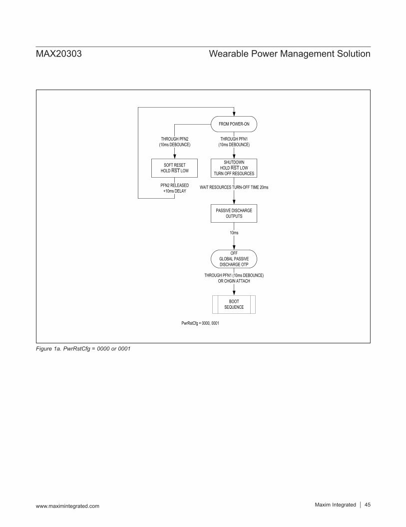
Figure 1a. PwrRstCfg = 0000 or 0001
FROM POWER-ON
SHUTDOWNHOLD RST LOW
TURN OFF RESOURCES
THROUGH PFN1 (10ms DEBOUNCE)
WAIT RESOURCES TURN-OFF TIME 20ms
PASSIVE DISCHARGE OUTPUTS
10ms
OFFGLOBAL PASSIVE DISCHARGE OTP
THROUGH PFN1 (10ms DEBOUNCE)OR CHGIN ATTACH
SOFT RESETHOLD RST LOW
THROUGH PFN2 (10ms DEBOUNCE)
PFN2 RELEASED+10ms DELAY
BOOT SEQUENCE
PwrRstCfg = 0000, 0001
MAX20303 Wearable Power Management Solution
www.maximintegrated.com Maxim Integrated 45

Figure 1b. PwrRstCfg = 0010 or 0011
ON
SHUTDOWNHOLD RST LOW
TURN OFF RESOURCES
WAIT RESOURCES TURN OFF TIME 20ms
PASSIVE DISCHARGE OUTPUTS
10ms
OFFGLOBAL PASSIVE DISCHARGE OTP
CHGIN ATTACH
THROUGH PFN2 RISE/FALL(10ms DEBOUNCE)
BOOT SEQUENCE
PwrRstCfg = 0010, 0011
THROUGH PFN1 RISE/FALL(10ms DEBOUNCE)
HOLD RST LOWTURN OFF RESOURCES
WAIT RESOURCES TURN OFF TIME 20ms
ACTIVE DISCHARGE OUTPUTS
50ms
µC SOFTWARE RESET
HARD RESET
200ms DELAY
10ms DELAYSOFT RESET
200ms DELAY
HOLD RST LOW
THROUGH I2C PWR_OFF_CMDOR
I2C_PWR_OFF_DELY (30ms DELAY)
BOOT SEQUENCE
MAX20303 Wearable Power Management Solution
www.maximintegrated.com Maxim Integrated 46

Figure 1c. PwrRstCfg = 0100 or 0101
PwrRstCfg = 0100, 0101
ON
HOLD RST LOW,TURN RESOURCES OFF
ACTIVE DISCHARGE OUTPUTS
µC SOFTWARE RESET
BOOT SEQUENCE
SHUTDOWN :HOLD RST LOW,
TURN OFF RESOURCES ANDENABLE ACTIVE DISCHARGE
WAIT RESOURCE TURN -OFFTIME (20ms)
OFFGLOBAL PASSIVE DISCHARGE
(OTP)DISABLE ACTIVE DISCHARGE
SEAL HANDLER
HARD RESET PROCESSINITIATED
SOFT RESET PROCESSINITIATED
HOLD RST LOW
10ms DELAY
15s DELAY
ABORT HARD RESET
ABORT SOFT RESET
15s DELAY
PFN 2 LOW(10ms DEBOUNCE )
PFN 1 LOW(10ms DEBOUNCE )
PFN 1 HIGH (10ms DEBOUNCE )AND
CHGIN RISE /FALL (100ms DEBOUNCE )
PFN 2 HIGH (10ms DEBOUNCE )AND
CHGIN RISE /FALL (100ms DEBOUNCE )
I2C PWR _OFF_CMDOR
I2C_PWR _OFF_DLY (30ms DELAY )
CHGIN
50ms
WAIT RESOURCE TURN -OFF TIME(20ms)
15s EXPIRE
MAX20303 Wearable Power Management Solution
www.maximintegrated.com Maxim Integrated 47

Figure 1d. PwrRstCfg = 0110
ON
SHUTDOWNHOLD RST LOW
TURN OFF RESOURCES
WAIT RESOURCES TURN-OFF TIME 20ms
PASSIVE DISCHARGE OUTPUTS
10ms
OFFGLOBAL PASSIVE DISCHARGE OTP
VIA PFN1 LOW (10ms DEBOUNCE)OR CHGIN ATTACH
BOOT SEQUENCE
PwrRstCfg = 0110
THROUGH PFN1 LOW (10ms DEBOUNCE)
FOR 12sec
HOLD RST LOWTURN OFF RESOURCES
SHUTDOWNTRAP
PFN1 HIGH (10ms DEBOUNCE)
THROUGH I2C PWR_OFF_CMD ORI2C_PWR_OFF_DELY (30ms DELAY)
MAX20303 Wearable Power Management Solution
www.maximintegrated.com Maxim Integrated 48

Figure 1e. PwrRstCfg = 0111
ON
SHUTDOWNHOLD RST LOW
TURN OFF RESOURCES
WAIT RESOURCES TURN-OFF TIME 20ms
PASSIVE DISCHARGE OUTPUTS
10ms
OFFGLOBAL PASSIVE DISCHARGE OTP
THROUGH PFN 1 LOW 3sOR CHGIN ATTACH (28ms DEBOUNCE)
BOOT SEQUENCE
PwrRstCfg = 0111
THROUGH PFN1 LOW (10ms DEBOUNCE) FOR 10sec
SOFT RESETHOLD RST LOW
PFN1/2 RELEASE (10ms DEBOUNCE)+ 10ms DELAY
THROUGH I2C PWR_OFF_CMD ORI2C_PWR_OFF_DELY (30ms DELAY)
MAX20303 Wearable Power Management Solution
www.maximintegrated.com Maxim Integrated 49

Figure 1f. PwrRstCfg = 1000
ON
SHUTDOWNHOLD RST LOW
TURN OFF RESOURCES
WAIT RESOURCES TURN-OFF TIME 20ms
PASSIVE DISCHARGE OUTPUTS
10ms
OFFGLOBAL PASSIVE
DISCHARGE IF ENABLED
THROUGH PFN1 LOW FOR 3sOR CHGIN ATTACH (28ms DEBOUNCE)
BOOT SEQUENCE
PwrRstCfg = 1000
THROUGH PFN2 LOWFOR 12sec
SOFT RESETHOLD RST LOW
PFN2 RELEASE (10ms DEBOUNCE)+
10ms DELAY
THROUGH I2C PWR_OFF_CMDOR
I2C_PWR_OFF_DELY (30ms DELAY)
MAX20303 Wearable Power Management Solution
www.maximintegrated.com Maxim Integrated 50

Table 1. PwrRstCfg SettingsPwrRstCfg PFN1 PFN1 PU/PD PFN2 PFN2 PU/PD Notes
0000 Enable PulldownSoft-Reset Active-Low Pullup
On/Off mode with 10ms debounce. Active-high On/Off control on PFN1. Logic-low on PFN2 generates 10ms pulse on RST.Note: In this mode, if PFN1 is high, PWR_OFF_CMD will cause the part to turn off, then immediately return to the ON state.
0001 Disable PullupSoft-Reset Active-Low Pullup
On/Off mode with 10ms debounce. Active-low On/Off control on PFN1. Logic-low on PFN2 generates 10ms pulse on RST.Note: In this mode, if PFN1 is high, PWR_OFF_CMD will cause the part to turn off, then immediately return to the ON state.
0010 Hard-Reset Active-High Pulldown Soft-Reset
Active-High Pulldown
Always-On mode (i.e., device can only be put in Off state through PWR_OFF_CMD). 10ms hard reset off time. 10ms soft reset pulse time. 200ms delay prior to both reset behaviors.
0011 Hard-Reset Active-Low Pullup
Soft-Reset Active-Low Pullup
Always-On mode (i.e., device can only be put in Off state through PWR_OFF_CMD). 50ms Hard-Reset off time. 10ms Soft-Reset pulse time. 200ms delay prior to both reset behaviors.
0100
Hard-Reset Active-High Triggered on
CHGIN Insertion
Pulldown
Soft-Reset Active-High Triggered on
CHGIN Insertion
Pulldown
Always-On mode (i.e., device can only be put in Off state through PWR_OFF_CMD). 50ms Hard-Reset off time. 10ms Soft-Reset pulse time. 15s delay prior to both reset behaviors. Either reset may be aborted
0101
Hard-Reset Active-Low
Triggered by CHGIN Insertion
Pullup
Soft-Reset Active-Low
Triggered on CHGIN Insertion
Pullup
Always-On mode (i.e., device can only be put in Off state through PWR_OFF_CMD). 70ms Hard-Reset off time. 10ms Soft-Reset pulse time. 15s delay prior to both reset behaviors. Either reset may be aborted.
0110 KIN Pullup KOUT NoneOff mode through specific long-press (12s) or PWR_OFF_CMD. On mode through specific short-press (400ms).
0111 KIN Pullup KOUT None
Off mode through PWR_OFF_CMD. On mode through specific long-press (3s) or CHGIN insertion soft reset through specific long press (10s).
1000 KIN PullupSoft-Reset
Active-Low 12s Long Press
Pullup
Custom Two Button. Off mode through PWR_OFF_CMD. On mode through KIN long-press (3s) or CHGIN insertion. Soft reset through PFN2 long press (12s).
1001-1111 RFU
MAX20303 Wearable Power Management Solution
www.maximintegrated.com Maxim Integrated 51

Figure 2. The full MAX20303 Boot Sequence
FROM POWER ON
VBUS PRESENT?
FUEL GAUGE: ONWAIT FOR 30ms
CHARGER: OFF
LIMITER: ON
WAIT FOR 10ms
SYS_UVLO = 0?
LIMITER: OFFTshdnTmo = 0?
ERROR MODE(OUTPUTS AS OFF MODE)
POWER PATH: OFFCHARGER ENABLE: OFF
ENTER IN POWER OFF LATCHED, REQUIRES EXTERNAL EVENT TO
RESTART
WAIT TshdnTmo
CHARGER: OFF
POWER PATH: ON
BATOC ONBATOC Irq Ena
SYS_UVLO = 0?
CHG_ENA = ChgEn
Seq BASED STARTUP SEQUENCE
SYS_UVLO = 0? RST
SYS_UVLO Irq Ena
ON
NO
YES
YES
YESNO
NO
NO
VBUS REMOVAL
YES
YES
NO
V BUS
INSE
RTIO
N OR
PFN
PRE
SS
IF VBUS NOT PRESENT BEFORE TshdnTmo
SYS_UVLO Irq
BATOC Irq
MAX20303 Wearable Power Management Solution
www.maximintegrated.com Maxim Integrated 52

Power SequencingThe sequencing of the switching regulators, LDOs, and charge pump during power-on is configurable. See each regulator’s sequencing bits for details. Regulators can turn on at one of three points during the power-on process: 75ms after the power-on event, at the time the RST signal is released, or at two points in between. The two points between SYS and RST are fixed proportionally to the duration of the Power-On Reset (POR) process (tRST). The timing relationship is presented graphically in Figure 3.Alternatively, the regulators can remain off by default and turn on with an I2C command after RST is released.
LDO2 can be configured to be always-on as long as SYS or BAT is present.The SYS voltage is monitored during the power-on sequence. If VSYS falls below VSYS_UVLO_F during the sequencing process with a valid voltage at CHGIN, the process repeats from the point where SYS was enabled to allow more time for the voltage to stabilize. If there is not a valid voltage at CHGIN, the device returns to the OFF state to avoid draining the battery. Power is also turned off if BAT experiences a current greater than IBAT_OC_R for more than tBAT_OC_D.
Figure 3. Reset Sequence Programming
MAX20303 Wearable Power Management Solution
www.maximintegrated.com Maxim Integrated 53

Current SinkIn addition to several voltage regulators, the MAX20303 also includes three low-dropout linear current regulators from LED_ to GND. The sink current of each current regulator is independently programmable through its respective LED_ISet[4:0] bits in direct registers LED_Direct (0x2D–0x2F). The current regulators can be programmed to sink 0.6mA to 30mA with configurable step sizes and are ideal for sinking current from external LEDs. The LEDIStep[1:0] bits in direct register LEDStepDirect (0x2C) control the size of the current steps for all current sinks. This step size also sets an effective limit on the sinking current as the number of steps remains constant while the step size varies. Current sinks are enabled through an I2C command, by an internal charger status signal, or by an external MPC pin allowing for LED status indicators. Note that the current sinks always draw quiescent current when tied to an MPC_ control or status signal regardless of the MPC_ or status state.
System Load SwitchAn internal 80mΩ (typ) MOSFET connects BAT to SYS when no voltage source is available on CHGIN. When an external source is detected at CHGIN, this switch opens and SYS is powered from the input source through the input current limiter. The SYS-to-BAT switch also prevents VSYS from falling below VBAT when the system load exceeds the input current limit. If VSYS drops to VBAT due to the current limit, the BAT-SYS switch turns on so the load is supported by the battery. If the system load continuously exceeds the input current limit, the battery is not charged. This is useful for handling loads that are nominally below the input current limit but have high current peaks exceeding the input current limit. During these peaks, battery energy is used, but at all other times the battery charges.
Smart Power SelectorThe smart power selector seamlessly distributes power from the external CHGIN input to the BAT and SYS nodes. With both an external adapter and battery connected, the smart power selector basic functions are:
When the system load requirements are less than the input current limit, the battery is charged with residual power from the input.
When the system load requirements exceed the input current limit, the battery supplies supplemental current to the load.
When the battery is connected and there is no external power input, the system is powered from the battery.
Input LimiterThe input limiter distributes power from the external adapter to the system load and battery charger. In addition to the input limiter’s primary function of passing power to the system load and charger, it performs several additional functions to optimize use of available power.Invalid CHGIN Voltage Protection: If CHGIN is above the overvoltage threshold, the device enters overvoltage lockout (OVL). OVL protects the MAX20303 and down-stream circuitry from high-voltage stress up to +28V and down to -5.5V. During positive OVL, the internal circuit remains powered and an interrupt is sent to the host. The negative voltage protection disconnects CHGIN and the device is powered only by BAT. The charger turns off and the system load switch closes, allowing the battery to power SYS. CHGIN is also invalid if it is less than VBAT, or less than the USB undervoltage threshold. With an invalid input voltage, the BAT-SYS load switch closes and allows the battery to power SYS.CHGIN Input Current Limit: The CHGIN input current is limited to prevent input overload. The input current limit is controlled by I2C. To accommodate systems with a high in-rush current, the limiter includes a program-mable blanking time during which the input current limit increases to ILIM_MAX.Thermal Limiting: In case the die temperature exceeds the normal limit (TCHG_LIM), the MAX20303 attempts to limit temperature increase by reducing the input current from CHGIN. In this condition, the system load has priority over the charger current, so the input current is first reduced by lowering the charge current. If the junction temperature continues to rise and reaches the maximum operating limit (TCHGIN_SHDN), no input current is drawn from CHGIN and the battery powers the entire system load.Adaptive Battery Charging: While the system is powered from CHGIN, the charger draws power from SYS to charge the battery. If the total load exceeds the input current limit, an adaptive charger control loop reduces charge current to prevent VSYS from collapsing. When the charge current is reduced below 50% due to ILIM or TCHG_LIM limits, the timer clock operates at half speed. When the charge current is reduced below 20% due to ILIM or TCHG_LIM limits, the timer clock is paused.Fast-Charge Current Setting: The MAX20303 uses an external resistor connected from SET to GND to set the fast-charge current. The precharge and charge-termina-tion currents are programmed as a percentage of this value by opcode 0x14. The fast-charge current resistor can be calculated as:
RSET = KSET x VSET/IFChg
MAX20303 Wearable Power Management Solution
www.maximintegrated.com Maxim Integrated 54

where KSET has a typical value of 2000A/A and VSET has a typical value of +1V. The range of acceptable resistors for RSET is 4kΩ to 400kΩ.A capacitive load on SET can cause instability of the charger if the condition (CSET < 5μs/RSET) pF is violated.
SAR ADC/Monitor MUXIn order to simplify system monitoring, the MAX20303 includes a voltage monitor multiplexer (MUX). The I2C controlled MUX connects the MON pin to the scaled value of one of six voltage regulators, BAT, or SYS. A resistive divider scales the voltage to one of four ratios determined by MONRatioCfg[1:0] (opcode 0x50, Table 117). Because the MUX can only tolerate voltages up to +5.5V, VCHGIN, VCPOUT, and VBSTOUT are not available to MON.An internal ADC reads the remaining voltage rails and performs system tasks such as JEITA temperature monitoring and SYS tracking during haptic driver operations. Manual ADC measurements are initiated by writing the desired channel to ADC_Measure_Launch (opcode 0x53, Table 121) and reading the response from APDataIn0-3. The ADC can also measure the MON voltage when the MUX is enabled with a 1:1 ratio. The full-scale range of the ADC for different voltage rails is detailed in Table 2.
JEITA Monitoring with Charger ControlTo enhance safety when charging Li+ batteries, the MAX20303 includes JEITA-compliant temperature monitoring. A resistive divider is formed on THM by attaching a pullup resistor to TPU and connecting the thermistor of a battery-pack (do not exceed 1mA load on TPU). The divider output is read by the internal ADC when JEITA monitoring is enabled and the result-ing temperature measurement places the battery into one of
five temperature zones: cold, cool, room, warm, and hot. Zone-specific temperature limits and charging behavior are fully configurable through the ChargerThermalLimits_Config_Write (opcode 0x16, Table 69) and ChargerThermalReg_Config_Write (opcode 0x18, Table 73) commands detailed in Table 69 and Table 73. Some example profiles are included in Figure 4. It is important to note that, because battery temperature is measured by the internal ADC, JEITA moni-toring is unavailable when automatic level compensation is enabled in the haptic driver.
Haptic DriverThe MAX20303 features a versatile, integrated haptic driver. The driver allows for real time control of haptic devices through PWM or I2C as well as the ability to run haptic patterns from internal RAM. For added flexibility, the driver is capable of driving both Linear Resonant Actuator (LRA) and Eccentric Rotating Mass (ERM) actuators.
Figure 4a. Sample JEITA Pre Charge Profile Figure 4b. Sample JEITA Fast Charge Profile
Table 2. SAR ADC Full-Scale Voltages and Conversions
VOLTAGE RAIL
AVAILABLE RANGE CONVERSION (V)
SYS +2.6V to +5.5V (Result[7:0] * 5.5)/255
MON 0V to +5.5V (Result[7:0] * 5.5)/255
THM 0% to 100% VDIG (Result[7:0] * 100)/255
CHGIN +3V to +8V (Result[7:0] * 8.25)/255
CPOUT +3V to +8V (Result[7:0] * 8.25)/255
BSTOUT +3V to +21V (Result[7:0] * 21.0)/255
ICOLDFChg
ICOOLFChg IWARMFChgIHOTFChg
ColdChgEn CoolChgEn WarmChgEn HotChgEn
CHARGING
T1 T2 T3 T4
IROOMFChg
TEMPERATURE (°C)
FAST CHARGE CONSTANT CURRENT:VBAT_PCHG < VBAT < VBAT_REG
ColdChgEn = 0 CoolChgEn WarmChgEn HotChgEn = 0CHARGING
T1 T2 T3 T4
IPCHG
TEMPERATURE (°C)
PREQUAL:VBAT < VBAT_PCHG
IPCHG IPCHG
MAX20303 Wearable Power Management Solution
www.maximintegrated.com Maxim Integrated 55

Figure 4c. Sample JEITA Maintain Charge Profile
Figure 5. Charger State Diagram
ColdBatReg CoolBatReg HotBatReg
ColdEn CoolEn WarmEn HotEn
CHARGING
T1 T2 T3 T4
BatReg
TEMPERATURE (°C)
WarmBatReg
MAINTAIN:VBAT ≥ BatReg- BatReChg
TIMER FAULT
ChgStat = 111LED = 0.15s PERIOD
ICHG = 0ChgEn = 1,
VBAT < VBATREG – VBATRECHGAND VSYS > VFCHG-MTCHG
RISE
VBAT>VPCHG_RRESET CHARGE TIMER
VBAT < VPCHG_RRESET CHARGE TIMER
VOLTAGE MODE = 1* AND VSYS > VFCHG-MTCHG
RISE
JEITA ENABLE CHARGING
JEITA DISABLE CHARGING
RESET CHARGE TIMERJEITA ENABLE CHARGING
JEITA DISABLE CHARGING
ChgEn=1,VBAT > VBATREG – VBATRECHG
ChgEn = 1,VBAT > VBATREG – VBATRECHG
ICHG > ICHG_DONE RESET CHARGE TIMER
ICHG < ICHG_DONE AND VSYS > VFCHG-MTCHG RISE
AND TDIE < TCHG_LIMRESET CHARGE TIMER
VOLTAGE MODE=0* AND VSYS > VFCHG-MTCHG
RISE OR VBAT < VPCHG_R
tCHG_TIMER > tMTCHGAND ChgAutoStp=1
VBAT < VBATREG – VBATRECHGAND ChgAutoReSta = 1
AND VSYS < VFCHG-MTCHG RISE RESET CHARGE TIMER
PAUSE CHARGE
TIMER
PAUSE CHARGE
TIMER
PAUSE CHARGE
TIMER
tCHG_TIMER > tPCHG
tCHG_TIMER > tFCHG
TDIE > TCHGIN_LIMOR VBAT > VSYSOR ChgEn = 0
OR INPUT LIMITER OFF
FROM ANY STATE
NOTES:
* VOLTAGE MODE IS AN INTERNAL SIGNAL
** CHARGE TIMER IS SLOWED BY 50% IF ICHG<IFCHG/2 AND PAUSED IF ICHG<IFCHG/5 ONLY IN FAST CHARGE CONSTANT CURRENT STATE
PREQUAL SUSPEND
ChgStat = 001LED = 1.5s PERIOD
ICHG = 0
FAST CHARGE CC SUSPEND
ChgStat = 001LED = 1.5s PERIOD
ICHG = 0
FAST CHARGE CV SUSPEND
ChgStat = 001LED = 1.5s PERIOD
ICHG = 0
FAST CHARGE CONSTANT VOLTAGE
ChgStat = 100LED = ON
ICHG = IFCHG
FAST CHARGE CONSTANT CURRENT
ChgStat = 011LED = ON
ICHG = IFCHG**
PREQUAL
ChgStat = 010LED = ON
ICHG = IPCHG
CHARGER OFF
ChgStat = 000LED = OFF
ICHG = 0
MAINTAIN CHARGE
ChgStat = 101LED = ON
ICHG < ICHG_DONE
MAINTAIN CHARGE DONE
ChgStat = 110LED = OFF
ICHG = 0
FRESH BATTERY INSERTION
ChgStat = 110LED = 1s PULSE
ICHG = 0
CHARGE SUSPEND
ChgStat = 001LED = 1.5s PERIOD
ICHG = 0
1s
JEITA DISABLE CHARGING
JEITA DISABLE CHARGING
T < T2 OR T > T3
tMTCHG
VBAT < VBATREG – VBATRECHG
JEITA DISABLE CHARGING
JEITA ENABLE CHARGING
JEITA ENABLE CHARGING
JEITA DISABLE CHARGING
MAX20303 Wearable Power Management Solution
www.maximintegrated.com Maxim Integrated 56

ERMAn ERM is the simplest haptic actuator to drive. The driving signal is taken directly as the output of an integrated H-bridge, allowing for bidirectional operation of the actuator. To configure the MAX20303 to drive an ERM, the HptSel bit must be set to 0 using the opcode 0xA0 or 0xAD (Table 127 and Table 153).
LRAUnlike the on-off control of an ERM, LRAs require a sinu-soidal driving signal. The MAX20303 realizes this with a Class-D amplifier that converts the driver input to a sinu-soidal output. Note that any changes made to the output amplitude take effect in the next period of the sinusoid.An LRA’s vibration magnitude is maximized when the driving signal matches the LRA’s resonant frequency. To ensure the haptic driver closely tracks this frequency, the MAX20303 includes an auto-resonance tracking feature. Resonance tracking is enabled by setting the EmfEn bit to 1 with opcode 0xA0 or 0xAD. The range of resonant frequencies that can be reliably driven is 120Hz to 305Hz. Enabling resonance tracking is strongly recommended when driving an LRA to ensure maximum driving efficiency and amplitude. To select LRA mode, set the HptSel bit to 1 using opcode 0xA0 or 0xAD.
Driver AmplitudeThe haptic driver features a configurable voltage basis for the amplitude of the driving signal. Setting this basis, referred to as the full-scale voltage (VFS), configures the maximum amplitude of the driver output. It is set using HptVfs[7:0] with opcode 0xA2 or 0xB2 (Table 131 and Table 163) and has a range of 0V to 5.5V (LSB = 21.57mV). Since the H-bridge is supplied by VSYS, the actual full-scale voltage of the driver at any given moment is the minimum of the value stored in HptVfs[7:0] and VSYS.Once VFS has been set, all driver amplitudes are scaled as a percentage of the full-scale voltage. The resolution of the amplitude is always VSYS/128. Therefore, the effective resolution of the amplitude scales with the VFS/VSYS ratio. For example, if VFS = VSYS/2, the effective resolution is 6 bits.
Automatic Level CompensationBecause VSYS can vary over time, the driver must adjust its output duty cycle to maintain a constant reference to the full-scale voltage. An Automatic Level Compensation (ALC) function measures VSYS and handles this adjustment. ALC can be enabled by setting the AlcMod bit to 1 using opcode
0xA0 or 0xAD and uses the MAX20303’s internal ADC to monitor VSYS. The ALC function then scales the haptic driver’s duty cycle as needed to maintain the programmed driver amplitude. If ALC is not enabled, VSYS is assumed to be VFS.
Haptic UVLOAdditionally, VSYS is measured after the driver is enabled but prior to starting a vibration. At any moment, if VSYS goes below the programmed UVLO value, which is set through HptSysUVLO[7:0] with opcode 0xA6 (Table 139), the vibration event is aborted and the haptic driver is locked. See the Haptic Driver Lock section for details regarding restarting vibration if a haptic UVLO condition is reached. The time required to perform the VSYS measurement, as well as other startup delays, results in an initial latency of the haptic driver. To avoid partial pattern skipping in real-time modes, vibration patterns should be provided at least tHD_START after enabling the desired real-time vibration mode (PPWM or RTI2C).
Vibration Timeout A vibration timeout parameter is programmable through I2C. If a vibration lasts longer than the programmed time-out period, the vibration is aborted. The timeout period is stored in HptDrvTmo[5:0] (LSB = 1s), which can be written using opcode 0xB7 (Table 173). Writing code “000000” disables the timeout function. See the Haptic Driver Lock section for details regarding restarting vibration if a timeout is reached.
Overcurrent/Thermal Protection The haptic driver also includes overcurrent and thermal shutdown protection. While the haptic driver is active, the MAX20303 monitors the current from DRP and DRN. If overcurrent protection is enabled (HptOCProtDis = 0) and the DRP or DRN current exceeds IHD_OC_THR, the haptic driver issues a fault, aborts vibration, and enters the locked state.Thermal protection allows the MAX20303 to immediately shut down the haptic driver should the die temperature exceed THD_OC_THR. This feature is enabled by setting HptThmProtDis = 0.See the Haptic Driver Lock section for details regarding restarting vibration if an overcurrent or overtemperature condition is reached.
MAX20303 Wearable Power Management Solution
www.maximintegrated.com Maxim Integrated 57

Haptic Driver LockIf the MAX20303 detects a fault in the haptic driver, vibrations in progress are aborted and the haptic driver is locked by the HptLock bit. The user must manually clear the HptLock bit using opcode 0xA8 (Table 143) in order to run a new vibration attempt. A fault occurs under any of the following conditions: VSYS drops below the threshold programmed in HptSysUVLO[7:0] (SystemError 0x25), an overcurrent is detected on DRN or DRP (SystemError = 0x20, 0x21, 0x22, or 0x23), the die temperature exceeds the thermal protection threshold (SystemError = 0x24), or a vibration duration exceeds the timeout period stored in HptDrvTmo[5:0] (SystemError 0x04). Writing any value other than 0x00 with opcode 0xA8 will set HptLock high and disable the driver output.
Interface ModesThere are a total of four interface modes for controlling the haptic driver. These include two real-time modes and two stored memory modes. The haptic driver mode is set through HptDrvMode[4:0] with the direct-access I2C register 0x31. Selecting an operation mode also enables the driver. In addition, HptDrvEn must be set and kept to 1 before setting HptDrvMode[4:0] and for the whole dura-tion of vibration. Once vibration finishes, HptDrvMode[4:0] must be set to “00000” before the haptic driver may be disabled via HptDrvEn = 0 for power savings.
Pure-PWM (PPWM)PPWM mode offers real-time control of the haptic driver. Patterns are generated by applying a PWM signal to the MPC_ pin selected by HptDrvMode[4:0]. The duty cycle of the applied signal determines the amplitude of the driving signal, scaled by VFS. The driving direction is centered about a 50% duty cycle. A duty cycle of 0% to 47.5% produces a (100 to 0)%VFS amplitude in the negative direction and a duty cycle of 52.5% to 100% produces a (0 to 100)%VFS amplitude in the positive direction. The region between 47.5% and 52.5% duty cycle is a dead zone and inputs within this range correspond to a null output.A timeout feature prevents idle PWM inputs from causing unwanted vibrations of the haptic motor. If the input signal remains at 0% duty cycle or 100% duty cycle for more than 2.56ms, the output is null and vibration stops. As such, the MPC_ input must remain dynamic to produce a continuous output.
Real-Time I2C (RTI2C)Similar to PPWM mode, RTI2C mode offers real-time control of the haptic driver. The direct register HptRTI2CAmp (0x32) determines the amplitude of the output signal. The lower seven bits of the register (HptRTI2CAmp[6:0]) set the amplitude as a percentage of VFS and the MSB (HptRTI2CSign) sets the direction of rotation. 100% amplitude, reverse drive, for example, is produced by setting HptRTI2CAmp to 0x7F (0b01111111).Once RTI2C mode is enabled through HptDrvMode[4:0], the haptic driver continuously outputs the amplitude and direction defined by the latest data in HptRTI2CAmp. In order to generate haptic patterns, the HptRTI2CAmp register must receive new data.
External Triggered Stored Pattern (ETRG)In ETRG mode, a rising edge on an MPC_ pin or a 0-to-1 transition of the HptExtTrig bit in direct I2C register 0x31 initiates a vibration sequence. The sequence is contained in six registers and comprises an overdrive (startup) amplitude, active drive amplitude, braking amplitude, and the duration of each driving behavior.Amplitudes contained in ETRGOdAmp[7:0], ETRGActAmp[7:0], and ETRGBrkAmp[7:0], which are set through opcode 0xA2–0xA4 or 0xB3 (Table 131 thru Table 136 and Table 165), follow the same format as HptRTI2CSign + HptRTI2CAmp[6:0] in direct I2C register 0x32 (i.e., the lower-seven bits store the amplitude as a percentage of VFS and the MSB determines the direction).The trigger input is selected when the driver enters ETRG mode via HptDrvMode[4:0] in direct I2C register 0x31. In order to properly register the rising edge, the trigger signal must remain high for a few clock cycles of the driver. Once the sequence begins, the haptic driver follows the duration values stored in ETRGOdDur[7:0], ETRGActDur[7:0], and ETRGBrkDur[7:0]. It is possible, however, to extend the active drive time by leaving the trigger high longer than the time specified in ETRGActDur[7:0]. Doing so will cause the driver to output the amplitude stored in ETRGActAmp[7:0] until a falling edge is detected. Once the trigger signal falls low, the brake sequence executes.
RAM Stored Haptic Pattern (RAMHP)The final method of controlling the haptic driver is RAMHP mode. The MAX20303 contains an internal 256 x 24 bit RAM in which haptic patterns are stored. By storing haptic sequences in RAM at startup, the driver can perform sophisticated haptic sequences upon receipt of a trigger signal as in ETRG mode. The direct I2C register HptPatRAMAddr (0x33) specifies the RAM address where the sequence begins.
MAX20303 Wearable Power Management Solution
www.maximintegrated.com Maxim Integrated 58

RAM should be loaded when the MAX20303 comes out of Off mode. To write data to the RAM, the HptRAMEn bit in direct register HptDirect1 (0x31) must first be set high. Next, writing a value to the direct register HptRAMAddr (0x28) specifies the RAM address in which data written to HptDataH, HptDataM, and HptDataL (0x29, 0x2A, and 0x2B, respectively) is stored. It is possible to read back data from RAM. Writing an address to HptRAMAddr, then initiating an I2C read transaction of register 0x29, will allow readback of the three bytes stored in the RAM address. RAM read and write procedures are depicted graphically in Figure 6.A haptic pattern is composed of multiple pattern samples. Pattern samples define the amplitude, duration, wait time, transition, and repetition of a segment of a haptic pattern.
These samples are defined in three bytes and written to RAM through HptDataH, HptDataM, and HptDataL. HptDataH contains the sign of the sample’s amplitude (AxSign), the upper-five bits of the amplitude (Ax[6:2]), and instructions to the haptic driver on handling the pattern sample (nLSx). HptDataM contains the lower two bits of the sample’s amplitude (Ax[1:0]), the duration of the sample (Dx), and the upper bit of the wait time before the next sample in the pattern (Wx[4]). HptDataL contains the lower four bits of the wait time (Wx[3:0]) and the repetition behavior (RPTx). Table 3 describes the definition of a pattern sample and Figure 7 provides a sample haptic pattern with corresponding waveform.
Figure 6. Read and Write Processes for RAM
S
FROM MASTER TO SLAVE
FROM SLAVE TO MASTER
ASLAVE ADDRESS-W P
WRITING RAM DATA BYTES AT RAM ADDRESS[7:0]
HptRAMAddr (0x28) A RAM ADDRESS[7:0] A RAMDataH[7:0] A RAMDataM[7:0] A RAMDataL[7:0] A
S ASLAVE ADDRESS-W P
READING RAM DATA BYTES FROM RAM ADDRESS[7:0]
HptDataH (0x29) A SLAVE ADDRESS-R A
S ASLAVE ADDRESS-W HptRAMAddr (0x28) A RAM ADDRESS[7:0] A
Sr RAMDataH[7:0] A RAMDataM[7:0] A RAMDataL[7:0] NA
S START CONDITION
Sr REPEATED START
P STOP CONDTION
ACKNOWLEDGEA
NA NOT ACKNOWLEDGE
MAX20303 Wearable Power Management Solution
www.maximintegrated.com Maxim Integrated 59

Table 3. RAMHP Pattern Storage FormatADDRESS 0x28-0x2BBIT B7 B6 B5 B4 B3 B2 B1 B0HptRAMAddr HptRAMAddr[7:0]
HptDataH nLSx[1:0] AmpSign Amp[6:2]
HptDataM Amp[1:0] Dur[4:0] Wait[4]
HptDataL Wait[3:0] RPTx[3:0]
HptRAMAddr [7:0] The RAM address in which the pattern sample is stored
nLSx[1:0]
Sets the behavior of a sample in the pattern.00 = Current sample is the last sample in the pattern01 = Current sample is not the last sample in the pattern10 = Interpolate current sample with next sample11 = Current sample is the last sample in the pattern. Repeat the entire pattern RPTx[3:0] times
AmpSign[1:0]Sign of haptic amplitude in current sample0 = Positive1 = Negative
Amp[6:2] Sets the amplitude of pattern sample x as a 7-bit percentage of VFS and a 1-bit direction. See HptVfs[7:0] in Table 131.
Dur[4:0]
Sets the duration of time the driver outputs the amplitude of the current sample in increments of 5ms00000 = 0ms00001 = 5ms...11110 = 150ms11111 = 155ms
Wait[4:0]
Sets the duration of time the driver waits at zero amplitude before the next sample in increments of 5ms00000 = 0ms00001 = 5ms...11110 = 150ms11111 = 155ms
RPTx[3:0]
Sets the number of times to repeat the sample before moving to the next sample in the pattern. If nLSx[1:0] = 11, this sets the number of times to repeat the whole pattern.0000 = Repeat 0 times0001 = Repeat 1 time…1110 = Repeat 14 times1111 = Repeat 15 times
MAX20303 Wearable Power Management Solution
www.maximintegrated.com Maxim Integrated 60

Fuel GaugeModelGauge Theory of OperationThe MAX20303 fuel gauge is based on the MAX17048 stand-alone fuel gauge and simulates the internal, non-linear dynamics of a Li+ battery to determine its State of Charge (SOC). The sophisticated battery model considers impedance and the slow rate of chemical reactions in the battery. ModelGauge performs best with a custom model, obtained by characterizing the battery at multiple discharge currents and temperatures to precisely model it. At power-on reset (POR), the ICs have a preloaded ROM model that performs well for some batteries. For more details on the fuel gauge, refer to the MAX17048 data sheet.
Fuel-Gauge PerformanceIn coulomb counter-based fuel gauges, SOC drifts because offset error in the current-sense ADC measurement accumulates over time. Instantaneous error can be very
small, but never precisely zero. Error accumulates over time in such systems (typically, 0.5%–2% per day) and requires periodic corrections. Some algorithms correct drift using occasional events and, until such an event occurs, the algorithm’s error is boundless:
Reaching predefined SOC levels near full or empty Measuring the relaxed battery voltage after a long
period of inactivity Completing a full charge/discharge cycle
ModelGauge requires no correction events because it uses only voltage, which is stable over time. The ModelGauge remains accurate despite the absence of any of the above events; it neither drifts nor accumulates error over time.To correctly measure performance of a fuel gauge as experienced by end-users, exercise the battery dynamically. Accuracy cannot be fully determined from only simple cycles.
Figure 7a. Sample Pattern Stored in RAM
Figure 7b. Haptic Driver Output of Stored Pattern
nLS0[1:0] Amp[7:0] Dur[4:0] Wait[4:0] Rpt[3:0]
nLSPREV AmpPREV DurPREV WaitPREV RptPREV
01 A0 00010 00001 0001
01 A1 00011 00000 0010
10 A2 00011 00000 X
10 A3 00011 00000 X
11 A4 DC 00010 0010
END OF PREVIOUSPATTERN
WAIT 10ms
30ms 30ms 30ms 30ms 30ms 30ms 30ms 30ms
WAIT 20ms WAIT 20msWAIT 10ms
20ms 20ms
SAMPLE 0 SAMPLE 1 SAMPLE 2 SAMPLE 3 SAMPLE 4 REPEAT PATTERN
A0 A1 A2 A3 A4
MAX20303 Wearable Power Management Solution
www.maximintegrated.com Maxim Integrated 61

Battery Voltage and State of ChargeOpen-circuit voltage (OCV) of a Li+ battery uniquely determines its SOC; one SOC can have only one value of OCV. In contrast, a given VCELL can occur at many differ-ent values of OCV because VCELL is a function of time, OCV, load, temperature, age, impedance, etc.; one value of OCV can have many values of VCELL. Therefore, one SOC can have many values of VCELL, so VCELL cannot uniquely determine SOC. Even the use of sophisticated tables to consider both voltage and load results in significant error due to the load transients typically experienced in a system. During charging or discharging, and for approximately 30 min after, VCELL and OCV differ substantially, and VCELL has been affected by the preceding hours of battery activity. ModelGauge uses voltage comprehensively.
Temperature CompensationFor best performance, the host microcontroller must measure battery temperature periodically, and compensate the RCOMP ModelGauge parameter accordingly, at least once per minute. Each custom model defines constants RCOMP0 (0x97, default), TempCoUp (-0.5, default), and TempCoDown (-5.0, default). To calculate the new value of CONFIG.RCOMP:// T is battery temperature (degrees Celsius)if (T > 20)
RCOMP = RCOMP0 + (T - 20) x TempCoUp;else
RCOMP = RCOMP0 + (T - 20) x TempCoDown;Impact of Empty-Voltage SelectionMost applications have a minimum operating voltage below which the system immediately powers off (empty voltage). When characterizing the battery to create a custom model, choose empty voltage carefully. Capacity unavailable to the system increases at an accelerating rate as empty voltage increases.To ensure a controlled shutdown, consider including operating margin into the fuel gauge based on some low threshold of SOC, for example shutting down at 3% or 5%. This utilizes the battery more effectively than adding error margin to empty voltage.Battery InsertionWhen the battery is first inserted into the system, the fuel-gauge IC has no previous knowledge about the battery’s SOC. Assuming that the battery is relaxed, the IC translates its first VCELL measurement into the best initial estimate
of SOC. Initial error caused by the battery not being in a relaxed state diminishes over time, regardless of loading following this initial conversion. While SOC estimated by a coulomb counter diverges, ModelGauge SOC converges, correcting error automatically. Initial error has no long-lasting impact.Battery Insertion DebounceAny time the IC powers on or resets (see the VRESET/ID Register (0x18) section), it estimates that OCV is the maximum of 16 VCELL samples (1ms each, full 12-bit resolution). OCV is ready 17ms after battery insertion, and SOC is ready 175ms after that.Battery Swap DetectionIf VCELL falls below VRST, the IC quick-starts once VCELL returns above VRST. This handles battery swap; the SOC of the previous battery does not affect that of the new one. See the Quick-Start and VRESET/ID Register (0x18) sections.Quick-StartIf the IC generates an erroneous initial SOC, the battery insertion and system power-up voltage waveforms must be examined to determine if a quick-start is necessary, as well as the best time to execute the command. The IC samples the maximum VCELL during the first 17ms. See the Battery Insertion Debounce section. Unless VCELL is fully relaxed, even the best sampled voltage can appear greater or less than OCV. Therefore, quick-start must be used cautiously.Most systems should not use quick-start because the ICs handle most startup problems transparently, such as intermittent battery-terminal connection during insertion. If battery voltage stabilizes faster than 17ms, do not use quick-start.The quick-start command restarts fuel-gauge calculations in the same manner as initial power-up of the IC. If the system power-up sequence is so noisy that the initial estimate of SOC has unacceptable error, the system microcontroller may be able to reduce the error by using quick-start. A quick-start is initiated by a rising edge on the QSTRT pin, or by writing 1 to the quick-start bit in the MODE register.Power-On Reset (POR)POR includes a quick-start, so only use it when the battery is fully relaxed. See the Quick-Start section. This command restores all registers to their default values. After this command, reload the custom model. See the CMD Register (0xFE) section.
MAX20303 Wearable Power Management Solution
www.maximintegrated.com Maxim Integrated 62

Hibernate ModeThe ICs have a low-power hibernate mode that can accu-rately fuel gauge the battery when the charge/discharge rate is low. By default, the device automatically enters and exits hibernate mode according to the charge/dis-charge rate, which minimizes quiescent current (below 5µA) without compromising fuel-gauge accuracy. The ICs can be forced into hibernate or active modes. Force the IC into hibernate mode to reduce power consumption in applications with less than C/4-rate maximum loading. For applications with higher loading, Maxim recommends the default configuration of automatic control of hibernate mode.In hibernate mode, the device reduces its ADC conversion period and SOC update to once per 45s. See the HIBRT Register (0x0A) section for details on how the IC automatically enters and exits hibernate mode.
Alert InterruptThe ICs can interrupt a system microcontroller with five configurable alerts. All alerts can be disabled or enabled with software. When the interrupt occurs, the system microcontroller can determine the cause from the STATUS register.When an alert is triggered, the IC drives the ALRT pin logic-low and sets CONFIG.ALRT = 1. The ALRT pin remains logic-low until the system software writes CONFIG.ALRT = 0 to clear the alert. The alert function is enabled by default, so any alert can occur immediately upon power-up. Entering sleep mode clears no alerts.
Sleep ModeIn sleep mode, the IC halts all operations, reducing current consumption to below 1µA. After exiting sleep mode, the IC continues normal operation. In sleep mode, the IC does not detect self-discharge. If the battery changes state while the IC sleeps, the IC cannot detect it, causing SOC error. Wake up the IC before charging or discharging. To enter sleep mode, write MODE.EnSleep = 1 and either:
Hold SDA and SCL logic-low for a period for tSLEEP. A rising edge on SDA or SCL wakes up the IC.Write CONFIG.SLEEP = 1. To wake up the IC, write CONFIG.SLEEP = 0. Other communication does not wake up the IC. POR does wake up the IC.Therefore, applications that can tolerate 4µA should use hibernate mode rather than Sleep mode.
I2C Interface The MAX20303 uses the two-wire I2C interface to communicate with a host microcontroller. The configura-tion settings and status information provided through this interface are detailed in the register descriptions. To simplify the use of existing code and drivers designed for interfacing with the ModelGauge fuel gauge, the MAX20303 appears as two devices on an I2C bus. The main device controlling the regulators, charger, and other system functions has the seven-bit slave address 0b0101000 (0x50 for writes, 0x51 for reads). Accessing the fuel gauge is done using the seven-bit slave address 0b0110110 (0x6C for writes, 0x6D for reads).
Applications InformationI2C InterfaceThe MAX20303 contains an I2C-compatible interface for data communication with a host controller (SCL and SDA). The interface supports a clock frequency of up to 400kHz. SCL and SDA require pullup resistors that are connected to a positive supply.
Start, Stop, And Repeated Start ConditionsWhen writing to the MAX20303 using I2C, the master sends a START condition (S) followed by the MAX20303 I2C address. After the address, the master sends the register address of the register that is to be programmed. The master then ends communication by issuing a STOP condition (P) to relinquish control of the bus, or a REPEATED START condition (Sr) to communicate to another I2C slave. See Figure 8.
Figure 8. I2C START, STOP and REPEATED START Conditions
SCL
SDA
S Sr P
MAX20303 Wearable Power Management Solution
www.maximintegrated.com Maxim Integrated 63

Slave AddressSet the Read/Write bit high to configure the MAX20303 to read mode. Set the Read/Write bit low to configure the MAX20303 to write mode. The address is the first byte of information sent to the MAX20303 after the START condition.
Bit TransferOne data bit is transferred on the rising edge of each SCL clock cycle. The data on SDA must remain stable during the high period of the SCL clock pulse. Changes in SDA while SCL is high and stable are considered control sig-nals (see the Start, Stop, And Repeated Start Conditions section). Both SDA and SCL remain high when the bus is not active.
Single-Byte WriteIn this operation, the master sends an address and two data bytes to the slave device (Figure 9). The following procedure describes the single byte write operation:The master sends a START conditionThe master sends the 7-bit slave address plus a write bit (low)The addressed slave asserts an ACK on the data lineThe master sends the 8-bit register addressThe slave asserts an ACK on the data line only if the address is valid (NAK if not)
The master sends 8 data bitsThe slave asserts an ACK on the data lineThe master generates a STOP condition
Burst WriteIn this operation, the master sends an address and mul-tiple data bytes to the slave device (Figure 10). The slave device automatically increments the register address after each data byte is sent, unless the register being accessed is 0x00, in which case the register address remains the same. The following procedure describes the burst write operation:The master sends a START conditionThe master sends the 7-bit slave address plus a write bit (low)The addressed slave asserts an ACK on the data lineThe master sends the 8-bit register addressThe slave asserts an ACK on the data line only if the address is valid (NAK if not)The master sends 8 data bitsThe slave asserts an ACK on the data lineRepeat 6 and 7 N-1 timesThe master generates a STOP condition
Figure 9. Write Byte Sequence
ADEVICE SLAVE ADDRESS-WS AREGISTER ADDRESS
P
FROM MASTER TO SLAVE
FROM SLAVE TO MASTER
A8 data bits
WRITE SINGLE BYTE
MAX20303 Wearable Power Management Solution
www.maximintegrated.com Maxim Integrated 64

Single Byte ReadIn this operation, the master sends an address plus two data bytes and receives one data byte from the slave device (Figure 11). The following procedure describes the single byte read operation:The master sends a START conditionThe master sends the 7-bit slave address plus a write bit (low)The addressed slave asserts an ACK on the data lineThe master sends the 8-bit register address
The slave asserts an ACK on the data line only if the address is valid (NAK if not)The master sends a REPEATED START conditionThe master sends the 7-bit slave address plus a read bit (high)The addressed slave asserts an ACK on the data lineThe slave sends 8 data bitsThe master asserts a NACK on the data lineThe master generates a STOP condition
Figure 10. Burst Write Sequence
Figure 11. Read Byte Sequence
FROM MASTER TO SLAVE
FROM SLAVE TO MASTER
ADEVICE SLAVE ADDRESS-WS AREGISTER ADDRESS
P
A8 DATA BITS - 2A8 DATA BITS - 1
A8 DATA BITS - N………………
BURST WRITE
FROM MASTER TO SLAVE
FROM SLAVE TO MASTER
ADEVICE SLAVE ADDRESS-R NA8 DATA BITS P
ADEVICE SLAVE ADDRESS-WS AREGISTER ADDRESS
Sr
READ SINGLE BYTE
MAX20303 Wearable Power Management Solution
www.maximintegrated.com Maxim Integrated 65

Burst ReadIn this operation, the master sends an address plus two data bytes and receives multiple data bytes from the slave device (Figure 12). The following procedure describes the burst byte read operation:The master sends a START conditionThe master sends the 7-bit slave address plus a write bit (low)The addressed slave asserts an ACK on the data lineThe master sends the 8-bit register addressThe slave asserts an ACK on the data line only if the address is valid (NAK if not)The master sends a REPEATED START conditionThe master sends the 7-bit slave address plus a read bit (high)The slave asserts an ACK on the data line
The slave sends 8 data bitsThe master asserts an ACK on the data lineRepeat 9 and 10 N-2 timesThe slave sends the last 8 data bitsThe master asserts a NACK on the data lineThe master generates a STOP condition
Acknowledge BitsData transfers are acknowledged with an acknowledge bit (ACK) or a not-acknowledge bit (NACK). Both the master and the MAX20303 generate ACK bits. To generate an ACK, pull SDA low before the rising edge of the ninth clock pulse and hold it low during the high period of the ninth clock pulse (see Figure 13). To generate a NACK, leave SDA high before the rising edge of the ninth clock pulse and leave it high for the duration of the ninth clock pulse. Monitoring for NACK bits allows for detection of unsuccessful data transfers.
Figure 12. Burst Read Sequence
Figure 13. Acknowledge
FROM MASTER TO SLAVE
FROM SLAVE TO MASTER
ADEVICE SLAVE ADDRESS-WS AREGISTER ADDRESS
P
A8 DATA BITS - 3A8 DATA BITS - 2
NA8 DATA BITS - N
ADEVICE SLAVE ADDRESS-R A8 DATA BITS - 1Sr
BURST READ
SCL
SDA
S
1 2 8 9
NOT ACKNOWLEDGE
ACKNOWLEDGE
MAX20303 Wearable Power Management Solution
www.maximintegrated.com Maxim Integrated 66

Application Processor InterfaceSeveral of the MAX20303’s functions are controlled by an Application Processor (AP). AP commands read and write configuration settings to the internal registers. Data transfer is handled by the AP controller and is triggered by writes to APCmdOut. There is a 5ms (typ), 9ms (max) latency associated with setting commands. This delay increases if the command requires additional processes such as ADC measurements, haptic autotune, etc. When the transfer is complete, INT goes low, APCmdResponseInt (bit seven of direct register Int2 (0x05)) is set, and the controller writes the value of the received opcode to APResponse. Reading the data in APResponse provides verification of the successful execution of an opcode.
AP WriteTo set configuration registers, data must first be written to the APDataOut0-5 registers. Tables 47 to 190 detail the functions of each APDataOut_ register for a given opcode. Once APDataOut0-5 contain the configuration bytes, writing an opcode to APCmdOut signals the controller to transfer data to the internal registers. Note that a write opcode only transfers the number of bytes defined by the command. The controller ignores the contents of all extra APDataOut_ registers. See Figure 14 for the structure of an AP write procedure with an APResponse opcode check.
AP ReadTo read a configuration register, APCmdOut is set to a read opcode. Read opcodes signal the controller to transfer the internal register contents to the APDataIn0-5 registers. When the transfer is complete, APDataIn0-5 contain the stored configuration settings or operation results and can be read over I2C. Because read opcodes expect no inputs, any data stored in APDataOut0-5 is ignored. Figure 15 illustrates the AP read processes.
AP LaunchCertain commands trigger additional functions in the MAX20303. These commands, such as ADC_Measure_Launch (opcode 0x53) and HPT_Autotune (opcode 0xAC), may require additional elaboration time for taking measurements and computing the result. When the process is complete, results may be read from APDataIn0-5 as in normal AP Read commands.
Write-Protected Commands and FieldsIf the factory configured bit WriteProtect is enabled, the AP commands InputCurrent_Config_Write (0x10), Charger_Config_Write (0x14), and Charger_ControlWrite (0x1A) are not accessible. If the application processor issues a request to one of these commands, the device will respond with the SysError code MA_SYSERROR_APCMD_WRITEPROTECT.A settings are also write protected, but it is possible to write these settings using an additional field in the command that contains a password.
Figure 14. Executing a Write Opcode and Reading the MAX20303 Response
Figure 15. Executing a Read Opcode and Reading the MAX20303 Response
START I2C WRITE
APDataOut_ PAYLOAD
AP COMMAND ELABORATION TIME(5ms TYP, 9ms MAX)
APCmdOut
APResponse
I2C STOP
AP WRITE COMMAND
I2C READ
START I2C WRITE
AP COMMAND ELABORATION TIME(5ms TYP, 9ms MAX)
APCmdOut
APResponse
I2C STOP
AP READ COMMAND
APDataIn PAYLOAD
I2C STOP
MAX20303 Wearable Power Management Solution
www.maximintegrated.com Maxim Integrated 67

Dire
ct A
cces
s I2
C R
egis
ter M
ap
REG
ISTE
R
AD
DR
ESS
REG
ISTE
R
NA
ME
R/W
B7
B6
B5
B4
B3
B2
B1
B0
0x00
Har
dwar
eID
RH
ardw
areI
D[7
:0]
0x01
Firm
war
eID
RFi
rmw
areI
D[7
:0]
0x03
Int0
CO
RTh
mS
tatIn
tC
hgS
tatIn
tIL
imIn
tU
sbO
VP
Int
Usb
OkI
ntC
hgTh
mS
dInt
Thm
Reg
Int
Chg
TmoI
nt
0x04
Int1
CO
RTh
mS
DIn
tB
stFl
tInt
Thm
Buc
k2In
tTh
mB
uck1
Int
UV
LOLD
O2I
ntU
VLO
LDO
1Int
Thm
LDO
2Int
Thm
LDO
1Int
0x05
Int2
CO
RA
PC
mdR
espI
ntS
ysE
rrIn
t—
LRA
Lock
Int
LRA
Act
Int
BB
stTh
mIn
tS
ysB
atLi
mIn
tC
hgS
ysLi
mIn
t
0x06
Sta
tus0
R—
—Th
mS
tat[2
:0]
Chg
Sta
t[2:0
]
0x07
Sta
tus1
R—
—IL
imU
sbO
VP
Usb
Ok
Chg
JEIT
AS
DC
hgJE
ITA
Reg
Chg
Tmo
0x08
Sta
tus2
RTh
mS
DB
stFl
tTh
mB
uck2
Thm
Buc
k1U
VLO
LDO
2U
VLO
LDO
1Th
mLD
O2
Thm
LDO
1
0x09
Sta
tus3
RA
pCm
dRes
pS
ysE
rr—
LRA
Lock
LRA
Act
BB
stTh
mS
ysB
atLi
mC
hgS
ysLi
m
0x0B
Sys
tem
Err
orR
Sys
tem
Err
or[7
:0]
0x0C
IntM
ask0
R/W
Thm
Sta
tIntM
Chg
Sta
tIntM
ILim
IntM
Usb
OV
PIn
tMU
sbO
kInt
MC
hgJE
ITA
SD
IntM
Chg
JEIT
A R
egIn
tMC
hgTm
oInt
M
0x0D
IntM
ask1
R/W
Thm
SdI
ntM
Bst
FltIn
tMTh
mB
uck2
IntM
Thm
Buc
k1In
tMU
VLO
LDO
2Int
MU
VLO
LDO
1Int
MTh
mLD
O2I
ntM
Thm
LDO
1Int
M
0x0E
IntM
ask2
R/W
ApC
mdR
espI
ntM
Sys
Err
IntM
—LR
ALo
ckIn
tMLR
AA
ctIn
tMB
Bst
Thm
IntM
SysB
atLi
mIn
tMC
hgS
ysLi
mIn
tM
0x0F
AP
Dat
aOut
0R
/WA
PD
ataO
ut0[
7:0]
0x10
AP
Dat
aOut
1R
/WA
PD
ataO
ut1[
7:0]
0x11
AP
Dat
aOut
2R
/WA
PD
ataO
ut2[
7:0]
0x12
AP
Dat
aOut
3R
/WA
PD
ataO
ut3[
7:0]
0x13
AP
Dat
aOut
4R
/WA
PD
ataO
ut4[
7:0]
0x14
AP
Dat
aOut
5R
/WA
PD
ataO
ut5[
7:0]
0x15
AP
Dat
aOut
6R
/WA
PD
ataO
ut6[
7:0]
0x17
AP
Cm
dOut
R/W
AP
Cm
dOut
[7:0
]
0x18
AP
Res
pons
eR
AP
Res
pons
e[7:
0]
0x19
AP
Dat
aIn0
RA
PD
ataI
n0[7
:0]
0x1A
AP
Dat
aIn1
RA
PD
ataI
n1[7
:0]
0x1B
AP
Dat
aIn2
RA
PD
ataI
n2[7
:0]
0x1C
AP
Dat
aIn3
RA
PD
ataI
n3[7
:0]
0x1D
AP
Dat
aIn4
RA
PD
ataI
n4[7
:0]
0x1E
AP
Dat
aIn5
RA
PD
ataI
n5[7
:0]
0x20
LDO
Dire
ctR
/W—
——
——
—LD
O2D
irEn
LDO
1DirE
n
0x21
MPC
Dire
ctW
rite
R/W
——
—M
PC
4Writ
eM
PC
3Writ
eM
PC
2Writ
eM
PC
1Writ
eM
PC
0Writ
e
MAX20303 Wearable Power Management Solution
www.maximintegrated.com Maxim Integrated 68

Dire
ct A
cces
s I2
C R
egis
ter M
ap (c
ontin
ued)
REG
ISTE
R
AD
DR
ESS
REG
ISTE
R
NA
ME
R/W
B7
B6
B5
B4
B3
B2
B1
B0
0x22
MPC
Dire
ctR
ead
R—
——
MP
C4R
ead
MP
C3R
ead
MP
C2R
ead
MP
C1R
ead
MP
C0R
ead
0x28
Hpt
RA
MA
ddr
R/W
Hpt
RA
MA
dd[7
:0]
0x29
Hpt
RA
MD
ataH
R/W
nLS
x[1:
0]A
mpS
ign
Am
p[6:
2]
0x2A
Hpt
RA
MD
ataM
R/W
Am
p[1:
0]D
ur[4
:0]
Wai
t[4]
0x2B
Hpt
RA
MD
ataL
R/W
Wai
t[3:0
]R
pt[3
:0]
0x2C
LED
Ste
pDire
ctR
/WLE
D2O
pen
LED
1Ope
nLE
D0O
pen
——
—LE
DIS
tep[
1:0]
0x2D
LED
0Dire
ctR
/WLE
D0E
n[2:
0]LE
D0I
Set
[4:0
]
0x2E
LED
1Dire
ctR
/WLE
D1E
n[2:
0]LE
D1I
Set
[4:0
]
0x2F
LED
2Dire
ctR
/WLE
D2E
n[2:
0]LE
D2I
Set
[4:0
]
0x30
Hpt
Dire
ct0
R/W
——
——
—H
ptO
ffIm
pH
ptTh
mPr
otD
isH
ptO
CP
rotD
is
0x31
Hpt
Dire
ct1
R/W
Hpt
Ext
Trig
Hpt
Ram
En
Hpt
Drv
En
Hpt
Drv
Mod
e[4:
0]
0x32
Hpt
RTI
2CA
mp
R/W
Hpt
RTI
2CS
ign
Hpt
RTI
2CA
mp
[6:0
]
0x33
Hpt
PatR
AMAd
drR
/WH
ptP
atR
AM
Add
r[7:0
]
MAX20303 Wearable Power Management Solution
www.maximintegrated.com Maxim Integrated 69

Table 4. HardwareID Register (0x00)
Table 5. FirmwareID Register (0x01)
Table 6. Int0 Register (0x03)
Table 7. Int1 Register (0x04)
Interrupt Registers
Direct Access I2C Register Descriptions
ADDRESS: 0x00MODE: Read OnlyBIT 7 6 5 4 3 2 1 0NAME HardwareID[7:0]HardwareID [7:0] HardwareID[7:0] bits show information about the hardware revision of the MAX20303
ADDRESS: 0x01MODE: Read OnlyBIT 7 6 5 4 3 2 1 0NAME FirmwareID[7:0]FirmwareID [7:0] FirmwareID[7:0] bits show information about the firmware revision of the MAX20303
ADDRESS: 0x03MODE: Clear On ReadBIT 7 6 5 4 3 2 1 0
NAME ThmStatInt ChgStatInt ILimInt UsbOVPInt UsbOkInt ChgThmS DInt ThmRegInt ChgTmoInt
ThmStatInt Change in ThmStat caused interrupt.ChgStatInt Change in ChgStat caused interrupt, or first detection complete after POR.ILimInt Input current limit caused interrupt.UsbOVPInt Change in USBOVP caused interrupt.
UsbOkIntChange in USBOk caused interrupt. Note: Registers written using opcodes 0x10, 0x14, 0x16, 0x18, 0x1A, and 0x1C are reset on charger insertion. After receiving a UsbOk interrupt, wait 10ms before writing any data using these opcodes. Failure to wait 10ms may result in the data being overwritten to the default.
ChgThmSDInt Change in ChgThmSD caused interrupt.ThmRegInt Change in ChgThmReg caused interrupt.ChgTmoInt Change in ChgTmoInt caused interrupt.
ADDRESS: 0x04MODE: Clear On ReadBIT 7 6 5 4 3 2 1 0
NAME ThmSDInt BstFltInt ThmBuck 2Int
ThmBuck 1Int
UVLOLDO 2Int
UVLOLDO 1Int
ThmLDO 2Int
ThmLDO 1Int
ThmSDInt Change in ThmSD caused interrupt.BstFltInt Change in BstFlt caused interrupt.ThmBuck2Int Change in ThmBuck2 caused interruptThmBuck1Int Change in ThmBuck1 caused interrupt.UVLOLDO2Int Change in UVLOLDO2 caused interrupt.UVLOLDO1Int Change in UVLOLDO1 caused interrupt.ThmLDO2Int Change in ThmLDO2 caused interrupt.ThmLDO1Int Change in ThmLDO1 caused interrupt.
MAX20303 Wearable Power Management Solution
www.maximintegrated.com Maxim Integrated 70

Table 8. Int2 Register (0x05)
Table 9. Status0 Register (0x06)Status Registers
ADDRESS: 0x05
MODE: Clear On Read
BIT 7 6 5 4 3 2 1 0
NAME APCmdRes pInt SysErrInt — LRALockInt LRAActInt BBstThmInt SysBatLimInt ChgSysLi
mInt
APCmdRespIntAP Command Response Interrupt0 = No new data available in APDataIn registers.1 = New data available in APDataIn registers.
SysErrIntSystem Error Interrupt0 = No new error1 = New Asynchronous System Error
LRALockInt LRA Lock InterruptChange in LRALock caused interrupt.
LRAActInt Change in LRAAct caused interrupt.
BBstThmInt Change in BBstThm caused interrupt.
SysBatLimInt Change in SysBatLim caused interrupt.
ChgSysLimInt Change in ChgSysLim caused interrupt.
ADDRESS: 0x06
MODE: Read Only
BIT 7 6 5 4 3 2 1 0
NAME — — ThmStat[2:0] ChgStat[2:0]
ThmStat[2:0]
Status of Thermistor Monitoring000 = T < T1001 = T1 < T < T2010 = T2 < T < T3011 = T3 < T < T4100 = T > T4101 = No thermistor detected/THM high due to external pull-up110 = NTC input disabled via ThmEn111 = Automatic monitoring disabled because CHGIN is not present. THM can still be measured by ADC_Measure_Launch
ChgStat[2:0]
Status of Charger Mode 000 = Charger off 001 = Charging suspended due to temperature (see battery charger state diagram) 010 = Pre-charge in progress011 = Fast-charge constant current mode in progress100 = Fast-charge constant voltage mode in progress101 = Maintain charge in progress 110 = Maintain charger timer done 111 = Charger fault condition (see battery charger state diagram)
MAX20303 Wearable Power Management Solution
www.maximintegrated.com Maxim Integrated 71

Table 10. Status1 Register (0x07)ADDRESS: 0x07
MODE: Read Only
BIT 7 6 5 4 3 2 1 0
NAME — — ILim UsbOVP UsbOk ChgJEITA SD
ChgJEITA Reg ChgTmo
ILimCHGIN Input Current Limit 0 = CHGIN input current below limit 1 = CHGIN input current limit active
UsbOVPStatus of CHGIN OVP0 = CHGIN overvoltage not detected1 = CHGIN overvoltage detected
UsbOkStatus of CHGIN Input 0 = CHGIN Input not present or outside of valid range1 = CHGIN Input present and valid
ChgJEITASDStatus of Thermal Shutdown 0 = Charger in normal operating mode1 = Charger is in thermal shutdown
ChgJEITAReg
Status of Thermal Regulation0 = Charger is functioning normally, or disabled1 = Charger is running in thermal regulation mode and charging current is being actively reduced according to JEITA settings
ChgTmoStatus of Time-Out Condition0 = Charger is running normally, or disabled1 = Charger has reached a time-out condition
MAX20303 Wearable Power Management Solution
www.maximintegrated.com Maxim Integrated 72

Table 11. Status2 Register (0x08)
Table 12. Status3 Register (0x09)
ADDRESS: 0x08
MODE: Read Only
BIT 7 6 5 4 3 2 1 0
NAME ThmSD BstFlt ThmBuck2 ThmBuck1 UVLOLD O2 UVLOLDO1 ThmLDO2 ThmLDO1
ThmSD 0 = Device operating normally1 = Device in thermal shutdown
BstFlt 0 = HV Boost operating normally1 = HV Boost in fault mode due to overcurrent or thermal shutdown
ThmBuck2 0 = Buck2 operating normally1 = Buck2 in thermal shutdown
ThmBuck1 0 = Buck1 operating normally1 = Buck1 in thermal shutdown
UVLOLDO2 0 = LDO2 operating normally1 = LDO2 UVLO active
UVLOLDO1 0 = LDO1 operating normally1 = LDO1 UVLO active
ThmLDO2 0 = LDO2 operating normally1 = LDO2 in thermal shutdown
ThmLDO1 0 = LDO1 operating normally1 = LDO1 in thermal shutdown
ADDRESS: 0x09
MODE: Read Only
BIT 7 6 5 4 3 2 1 0
NAME APCmdResp SysErr — LRALock LRAAact BBstThm SysBatLim ChgSysLim
APCmdRespAP Command Response Ready0 = APResponse register is empty1 = APResponse register contains an opcode
SysErrSystem Error Detect0 = No system error1 = System error detected. See SystemError (register 0x0B)
LRALock 0 = Haptic driver is not active or has not yet locked onto LRA resonant frequency1 = Haptic driver has locked onto LRA resonant frequency
LRAAct 0 = LRA driver not active1 = LRA driver active
BBstThm 0 = Buck-boost converter operating normally1 = Buck-boost converter in thermal shutdown
SysBatLim 0 = Charge current is not being actively reduced to regulate SYS1 = Charge current actively being reduced to regulate SYS collapse
ChgSysLim 0 = Input current limit normal1 = Input current limit being reduced to regulate CHGIN collapse
MAX20303 Wearable Power Management Solution
www.maximintegrated.com Maxim Integrated 73

Table 13. SystemError Register (0x0B)ADDRESS: 0x0B
MODE: Read Only
BIT 7 6 5 4 3 2 1 0
NAME SystemError[7:0]
SystemError[7:0]
Last System Error Code:0x00 - MA_SYSERROR_NONE: No System Error0x01 - MA_SYSERROR_BOOT: 0x02 - MA_SYSERROR_BOOT_WDT: Restart due to a watchdog event0x03 - MA_SYSERROR_BOOT_SWRSTREQ: Restart after Hard-Reset procedure0x04 - MA_SYSERROR_HPT_TIMEOUT: Haptic driver disabled after timeout set through HptDrvTmo[5:0] has expired
0x10 - MA_SYSERROR_APCMD_INPROGRESS: Attempt to use an AP command before previous command completed0x11 - MA_SYSERROR_APCMD_WRITEPROTECT: Attempt to use a write protected command or invalid password0x12 - MA_SYSERROR_APCMD_UNKNOWN: Attempt to use an undefined command0x13 - MA_SYSERROR_APCMD_FAIL: AP command failed to execute
0x20 - MA_SYSERROR_HPT_DRP_LOW: Haptic driver disabled due to overcurrent condition on the DRP low-side switch0x21 - MA_SYSERROR_HPT_DRP_HIG: Haptic driver disabled due to overcurrent condition on the DRP high-side switch0x22 - MA_SYSERROR_HPT_DRN_LOW: Haptic driver disabled due to overcurrent condition on the DRN low-side switch0x23 - MA_SYSERROR_HPT_DRN_HIG: Haptic driver disabled due to overcurrent condition on the DRN high-side switch0x24 - MA_SYSERROR_HPT_THM_ERR: Haptic driver disabled due to thermal shutdown0x25 - MA_SYSERROR_HPT_SYS_THR_HIT: Haptic driver disabled due to SYS falling below HptSysUVLO[7:0] threshold
MAX20303 Wearable Power Management Solution
www.maximintegrated.com Maxim Integrated 74

Table 14. IntMask0 Register (0x0C)Interrupt Mask Registers
ADDRESS: 0x0C
MODE: Read/Write
BIT 7 6 5 4 3 2 1 0
NAME ThmStat IntM
ChgStat IntM ILimIntM UsbOVP
IntMUsbOk IntM
ChgJEITASD IntM
ThmJEITA RegIntM
ChgTmo IntM
ThmStatIntMThmStatIntM masks the ThmStatInt interrupt in the Int0 register (0x03). 0 = Masked 1 = Not masked
ChgStatIntMChgStatIntM masks the ChgStatInt interrupt in the Int0 register (0x03).0 = Masked1 = Not masked
ILimIntMILimIntM masks the ILimInt interrupt in the Int0 register (0x03). 0 = Masked1 = Not masked
UsbOVPIntMUsbOVPIntM masks the UsbOVPInt interrupt in the Int0 register (0x03). 0 = Masked 1 = Not masked
UsbOkIntMUsbOkIntM masks the UsbOkInt interrupt in the Int0 register (0x03). 0 = Masked 1 = Not masked
ChgJEITASDIntMChgThmSDIntM masks the ChgThmSDInt interrupt in the Int0 register (0x03). 0 = Masked1 = Not masked
ChgJEITARegIntMThmRegIntM masks the ThmRegInt interrupt in the Int0 register (0x03). 0 = Masked 1 = Not masked
ChgTmoIntMChgTmoIntM masks the ChgTmoInt interrupt in the Int0 register (0x03). 0 = Masked1 = Not masked
MAX20303 Wearable Power Management Solution
www.maximintegrated.com Maxim Integrated 75

Table 15. IntMask1 Register (0x0D)ADDRESS: 0x0D
MODE: Read/Write
BIT 7 6 5 4 3 2 1 0
NAME ThmSd IntM BstFltIntM ThmBuck
2IntMThmBuck
1IntMUVLOLDO
2IntMUVLOLDO
1IntMThmLDO
2IntMThmLDO
1IntM
ThmSdIntMThmSdIntM masks the ThmSdInt interrupt in the Int1 register (0x04). 0 = Masked 1 = Not masked
BstFltIntMBstFltIntM masks the BstFltInt interrupt in the Int1 register (0x04). 0 = Masked 1 = Not masked
ThmBuck2IntMThmBuck2IntM masks the ThmBuck2Int interrupt in the Int1 register (0x04). 0 = Masked 1 = Not masked
ThmBuck1IntMMasks the ThmBuck1Int interrupt in the Int1 register (0x04). 0 = Masked 1 = Not masked
UVLOLDO2IntMMasks the UVLOLDO2Int interrupt in the Int1 register (0x04). 0 = Masked 1 = Not masked
UVLOLDO1IntMMasks the UVLOLDO1Int interrupt in the Int1 register (0x04). 0 = Masked 1 = Not masked
ThmLDO2IntMMasks the ThmLDO2Int interrupt in the Int1 register (0x04). 0 = Masked 1 = Not masked
ThmLDO1IntMMasks the ThmLDO1Int interrupt in the Int1 register (0x04). 0 = Masked 1 = Not masked
MAX20303 Wearable Power Management Solution
www.maximintegrated.com Maxim Integrated 76

Table 16. IntMask2 Register (0x0E)ADDRESS: 0x0E
MODE: Read/Write
BIT 7 6 5 4 3 2 1 0
NAME APCmd RespIntM
SysErr IntM — LRALock
IntMLRAAct
IntMBBstThm
IntMSysBatLim
IntMChgSys LimIntM
APCmdRespIntMMasks the APCmdRespInt interrupt in the Int2 register (0x05). 0 = Masked 1 = Not masked
SysErrIntMMasks the SysErrInt interrupt in the Int2 register (0x05). 0 = Masked1 = Not masked
LRALockIntMMasks the LRALockInt interrupt in the Int2 register (0x05). 0 = Masked1 = Not masked
LRAActIntMMasks the LRAActInt interrupt in the Int2 register (0x05). 0 = Masked1 = Not masked
BBstThmIntMMasks the BBstThmInt interrupt in the Int2 register (0x05). 0 = Masked1 = Not masked
SysBatLimIntMMasks the SysBatLimInt interrupt in the Int2 register (0x05). 0 = Masked1 = Not masked
ChgSysLimIntMMasks the ChgSysLimInt interrupt in the Int2 register (0x05). 0 = Masked1 = Not masked
MAX20303 Wearable Power Management Solution
www.maximintegrated.com Maxim Integrated 77

Table 17. APDataOut0 Register (0x0F)
Table 18. APDataOut1 Register (0x10)
Table 19. APDataOut2 Register (0x11)
Table 20. APDataOut3 Register (0x12)
Table 21. APDataOut4 Register (0x13)
AP Interface Registers
ADDRESS: 0x0F
MODE: Read/Write
BIT 7 6 5 4 3 2 1 0
NAME APDataOut0[7:0]
APDataOut0[7:0] Data register 0 for AP write commands.
ADDRESS: 0x10
MODE: Read/Write
BIT 7 6 5 4 3 2 1 0
NAME APDataOut1[7:0]
APDataOut1[7:0] Data register 1 for AP write commands.
ADDRESS: 0x11
MODE: Read/Write
BIT 7 6 5 4 3 2 1 0
NAME APDataOut2[7:0]
APDataOut2[7:0] Data register 2 for AP write commands.
ADDRESS: 0x12
MODE: Read/Write
BIT 7 6 5 4 3 2 1 0
NAME APDataOut3[7:0]
APDataOut3[7:0] Data register 3 for AP write commands.
ADDRESS: 0x13
MODE: Read/Write
BIT 7 6 5 4 3 2 1 0
NAME APDataOut4[7:0]
APDataOut4[7:0] Data register 4 for AP write commands.
MAX20303 Wearable Power Management Solution
www.maximintegrated.com Maxim Integrated 78

Table 22. APDataOut5 Register (0x14)
Table 23. APDataOut6 Register (0x15)
Table 24. APCmdOut Register (0x17)
Table 25. APResponse Register (0x18)
Table 26. APDataIn0 Register (0x19)
Table 27. APDataIn1 Register (0x1A)
ADDRESS: 0x14
MODE: Read/Write
BIT 7 6 5 4 3 2 1 0
NAME APDataOut5[7:0]
APDataOut5[7:0] Data register 5 for AP write commands.
ADDRESS: 0x15
MODE: Read/Write
BIT 7 6 5 4 3 2 1 0
NAME APDataOut6[7:0]
APDataOut6[7:0] Data register 6 for AP write commands.
ADDRESS: 0x17
MODE: Read/Write
BIT 7 6 5 4 3 2 1 0
NAME APCmdOut[7:0]
APCmdOut[7:0] Opcode command register
ADDRESS: 0x18
MODE: Read Only
BIT 7 6 5 4 3 2 1 0
NAME APResponse [7:0]
APResponse[7:0] AP command response register
ADDRESS: 0x19
MODE: Read Only
BIT 7 6 5 4 3 2 1 0
NAME APDataIn0[7:0]
APDataIn0[7:0] Data register 0 for AP read commands.
ADDRESS: 0x1A
MODE: Read Only
BIT 7 6 5 4 3 2 1 0
NAME APDataIn1[7:0]
APDataIn1[7:0] Data register 1 for AP read commands.
MAX20303 Wearable Power Management Solution
www.maximintegrated.com Maxim Integrated 79

Table 28. APDataIn2 Register (0x1B)
Table 29. APDataIn3 Register (0x1C)
Table 30. APDataIn4 Register (0x1D)
Table 31. APDataIn5 Register (0x1E)
Table 32. LDODirect Register (0x20)LDO Direct Register
ADDRESS: 0x1B
MODE: Read Only
BIT 7 6 5 4 3 2 1 0
NAME APDataIn2[7:0]
APDataIn2[7:0] Data register 2 for AP read commands.
ADDRESS: 0x1C
MODE: Read Only
BIT 7 6 5 4 3 2 1 0
NAME APDataIn3[7:0]
APDataIn3[7:0] Data register 3 for AP read commands.
ADDRESS: 0x1D
MODE: Read Only
BIT 7 6 5 4 3 2 1 0
NAME APDataOut4[7:0]
APDataOut4[7:0] Data register 4 for AP write commands.
ADDRESS: 0x1E
MODE: Read Only
BIT 7 6 5 4 3 2 1 0
NAME APDataIn5[7:0]
APDataIn5[7:0] Data register 5 for AP read commands.
ADDRESS: 0x20
MODE: Read/Write
BIT 7 6 5 4 3 2 1 0
NAME — — — — — — LDO2Dir En
LDO1Dir En
LDO2DirEnLDO2 Direct Enable. Valid only if LDO2En = 110 = LDO2 Off1 = LDO2 On
LDO1DirEnLDO1 Direct Enable Valid only if LDO1En = 110 = LDO1 Off1 = LDO1 On
MAX20303 Wearable Power Management Solution
www.maximintegrated.com Maxim Integrated 80

Table 33. MPCDirectWrite Register (0x21)
Table 34. MPCDirectRead Register (0x22)
MPC Direct Registers
ADDRESS: 0x21
MODE: Read/Write
BIT 7 6 5 4 3 2 1 0
NAME — — — MPC4Write MPC3Write MPC2Write MPC1Write MPC0Write
MPC4WriteMPC4 Direct Write (returns 0 if MPC is configured as output (GPIO_HiZB = 1))0 = set MPC4 low1 = set MPC4 high
MPC3WriteMPC3 Direct Write (returns 0 if MPC is configured as output (GPIO_HiZB = 1))0 = set MPC3 low1 = set MPC3 high
MPC2WriteMPC2 Direct Write (returns 0 if MPC is configured as output (GPIO_HiZB = 1))0 = set MPC2 low1 = set MPC2 high
MPC1WriteMPC1 Direct Write (returns 0 if MPC is configured as output (GPIO_HiZB = 1))0 = set MPC1 low1 = set MPC1 high
MPC0WriteMPC0 Direct Write (returns 0 if MPC is configured as output (GPIO_HiZB = 1))0 = set MPC0 low1 = set MPC0 high
ADDRESS: 0x22
MODE: Read Only
BIT 7 6 5 4 3 2 1 0
NAME — — — MPC4Read MPC3Read MPC2Read MPC1Read MPC0Read
MPC4ReadMPC4 Direct Readback0 = MPC4 is low1 = MPC4 is high
MPC3ReadMPC3 Direct Readback0 = MPC3 is low1 = MPC3 is high
MPC2ReadMPC2 Direct Readback0 = MPC2 is low1 = MPC2 is high
MPC1ReadMPC1 Direct Readback0 = MPC1 is low1 = MPC1 is high
MPC0ReadMPC0 Direct Readback0 = MPC0 is low1 = MPC0 is high
MAX20303 Wearable Power Management Solution
www.maximintegrated.com Maxim Integrated 81

Table 35. HptRAMAddr Register (0x28)
Table 36. HptRAMDataH Register (0x29)
Table 37. HptRAMDataM Register (0x2A)
Table 38. HptRAMDataL Register (0x2B)
Haptic RAM Registers
ADDRESS: 0x28
MODE: Read/Write
BIT 7 6 5 4 3 2 1 0
NAME HptRAMAdd[7:0]
HptRAMAdd[7:0] RAM address to which haptic pattern data in registers 0x29, 0x2A, 0x2B will be written.
ADDRESS: 0x29
MODE: Read/Write
BIT 7 6 5 4 3 2 1 0
NAME nLSx[1:0] AmpSign Amp[6:2]
ADDRESS: 0x2A
MODE: Read/Write
BIT 7 6 5 4 3 2 1 0
NAME Amp[1:0] Dur[4:0] Wait[4]
ADDRESS: 0x2B
MODE: Read/Write
BIT 7 6 5 4 3 2 1 0
NAME Wait[3:0] Rpt[3:0]
MAX20303 Wearable Power Management Solution
www.maximintegrated.com Maxim Integrated 82

Table 39. LEDStepDirect Register (0x2C)
Table 40. LED0Direct Register (0x2D)
LED Direct Registers
ADDRESS: 0x2C
MODE: Read/Write
BIT 7 6 5 4 3 2 1 0
NAME LED2Open LED1Open LED0Open — — — LEDIStep[1:0]
LED2OpenLED2 Open detection (Read only)0 = VLED2 > VLED_DET 1 = VLED2 ≤ VLED_DET or LED2 disabled
LED1OpenLED1 Open detection (Read only)0 = VLED1 > VLED_DET 1 = VLED1 ≤ VLED_DET or LED1 disabled
LED0OpenLED0 Open detection (Read only)0 = VLED0 > VLED_DET 1 = VLED0 ≤ VLED_DET or LED0 disabled
LEDIStep[1:0]
LED Direct Current Step Register00 = 0.6mA01 = 1.0mA10 = 1.2mA11 = RESERVED
ADDRESS: 0x2D
MODE: Read/Write
BIT 7 6 5 4 3 2 1 0
NAME LED0En[2:0] LED0ISet[4:0]
LED0En[2:0]
LED0 Driver Enable000 = Off001 = LED0 On010 = Controlled by internal charger status signal011 = Controlled by MPC0100 = Controlled by MPC1101 = Controlled by MPC2110 = Controlled by MPC3111 = Controlled by MPC4
LED0ISet[4:0]
LED0 Direct Step CountLED0 current in mA is given by (LED0ISet[4:0] + 1) x LEDIStep[1:0]0x00 = 0.6mA/1.0mA/1.2mA0x01 = 1.2mA/2.0mA/2.4mA…0x18 = 15mA/25mA/30mA
MAX20303 Wearable Power Management Solution
www.maximintegrated.com Maxim Integrated 83

Table 41. LED1Direct Register (0x2E)
Table 42. LED2Direct Register (0x2F)
ADDRESS: 0x2E
MODE: Read/Write
BIT 7 6 5 4 3 2 1 0
NAME LED1En[2:0] LED1ISet[4:0]
LED1En[2:0]
LED1 Driver Enable000 = Off001 = LED1 On010 = Controlled by internal charger status signal011 = Controlled by MPC0100 = Controlled by MPC1101 = Controlled by MPC2110 = Controlled by MPC3111 = Controlled by MPC4
LED1ISet[4:0]
LED1 Direct Step CountLED1 current in mA is given by (LED1ISet[4:0] + 1) x LEDIStep[1:0]0x00 = 0.6mA/1.0mA/1.2mA0x01 = 1.2mA/2.0mA/2.4mA…0x18 = 15mA/25mA/30mA
ADDRESS: 0x2F
MODE: Read/Write
BIT 7 6 5 4 3 2 1 0
NAME LED2En[2:0] LED2ISet[4:0]
LED2En[2:0]
LED2 Driver Enable000 = Off001 = LED2 On010 = Controlled by internal charger status signal011 = Controlled by MPC0100 = Controlled by MPC1101 = Controlled by MPC2110 = Controlled by MPC3111 = Controlled by MPC4
LED2ISet[4:0]
LED2 Direct Step CountLED2 current in mA is given by (LED2ISet[4:0] + 1) x LEDIStep[1:0]0x00 = 0.6mA/1.0mA/1.2mA0x01 = 1.2mA/2.0mA/2.4mA…0x18 = 15mA/25mA/30mA
MAX20303 Wearable Power Management Solution
www.maximintegrated.com Maxim Integrated 84

Table 43. HptDirect0 Register (0x30)Haptic Direct Registers
ADDRESS: 0x30
MODE: Read/Write
BIT 7 6 5 4 3 2 1 0
NAME — — — — — HptOffImp HptThmProt Dis
HptOCPr otDis
HptOffImpHaptic Driver Output Off State Impedance0 = When haptic driver is disabled, outputs are strongly shorted to GND through low-side driver FETs.1 = When haptic driver is disabled, outputs are shorted to GND with 15kΩ pull-down.
HptThmProtDis
Haptic Driver Thermal Protection DisableIf HptThmProtDis = 0 and the haptic driver shuts down due to an over temperature condition, SystemError[7:0] = 0x24 is issued and HptLock = 1. See Opcode 0xA8 for restarting the haptic driver0 = Thermal protection enabled. Haptic driver will shut down if TJ ≥ 150°C (typ)1 = Thermal protection disabled.
HptOCProtDis
Haptic Driver Overcurrent Protection DisableIf HptOCProtDis = 0 and the haptic driver shuts down due to an overcurrent condition, SystemError[7:0] will equal to one of four codes (0x20-0x23) is issued and HptLock = 1. See Opcode 0xA8 for restarting the haptic driver0 = Overcurrent protection enabled. Haptic driver will shut down if current exceeds 1A (typ)1 = Overcurrent protection disabled.
MAX20303 Wearable Power Management Solution
www.maximintegrated.com Maxim Integrated 85

Table 44. HptDirect1 Register (0x31)ADDRESS: 0x31
MODE: Read/Write
BIT 7 6 5 4 3 2 1 0
NAME HptExtTrig HptRamEn HptDrvEn HptDrvMode[4:0]
HptExtTrig
Haptic driver external trigger pattern for ETRG and RAMHPI driver mode (HptDrvMode = 01100, 10010, respectively).0 = No pattern triggered.1 = Vibration triggered
HptRamEnHaptic RAM Block Enable0 = RAM disabled.1 = RAM enabled.
HptDrvEn
Haptic Driver EnableIn all modes, the haptic driver must be enabled at the same time or before providing the desired mode in HptDrvMod[4:0]. The HptDrvEn bit must remain set during the vibration. Once vibration finishes, HptDrvMod[4:0] must be set to “00000” before the haptic driver may be disabled via HptDrvEn = 0 for power savings.0 = Haptic driver block disabled.1 = Haptic driver block enabled.
HptDrvMode [4:0]
Haptic Driver Mode Selection00000 = Disable haptic driver00001 = Enable PPWM0 mode and provide amplitude based on PWM duty cycle on MPC000010 = Enable PPWM1 mode and provide amplitude based on PWM duty cycle on MPC100011 = Enable PPWM2 mode and provide amplitude based on PWM duty cycle on MPC200100 = Enable PPWM3 mode and provide amplitude based on PWM duty cycle on MPC300101 = Enable PPWM4 mode and provide amplitude based on PWM duty cycle on MPC400110 = Enable RTI2C mode and provide current output amplitude based on the contents of HptRTI2CAmp(0x32)00111 = Enable ETRG0 mode. Provide a pulse on MPC0 to start vibration (See “ETRG Mode” section for details)01000 = Enable ETRG1 mode. Provide a pulse on MPC1 to start vibration (See “ETRG Mode” section for details)01001 = Enable ETRG2 mode. Provide a pulse on MPC2 to start vibration (See “ETRG Mode” section for details)01010 = Enable ETRG3 mode. Provide a pulse on MPC3 to start vibration (See “ETRG Mode” section for details)01011 = Enable ETRG4 mode. Provide a pulse on MPC4 to start vibration (See “ETRG Mode” section for details)01100 = Enable ETRGI mode via I2C. Set HptExtTrg(0x31[7]) bit to start vibration (See “ETRG Mode” section for details)01101 = Enable RAMHP0 mode. Provide a pulse on MPC0 to start vibration (See “RAMHP Mode” section for details)01110 = Enable RAMHP1 mode. Provide a pulse on MPC1 to start vibration (See “RAMHP Mode” section for details)01111 = Enable RAMHP2 mode. Provide a pulse on MPC2 to start vibration (See “RAMHP Mode” section for details)10000 = Enable RAMHP3 mode. Provide a pulse on MPC3 to start vibration (See “RAMHP Mode” section for details)10001 = Enable RAMHP4 mode. Provide a pulse on MPC4 to start vibration (See “RAMHP Mode” section for details)10010 = Enable RAMHPI mode via I2C. Set HptExtTrg(0x31[7]) bit to start vibration (See “RAMHP Mode” section for details)
MAX20303 Wearable Power Management Solution
www.maximintegrated.com Maxim Integrated 86

Table 45. HptRTI2CAmp Register (0x32)
Table 46. HptPatRAMAddr Register (0x33)
ADDRESS: 0x32
MODE: Read/Write
BIT 7 6 5 4 3 2 1 0
NAME HptRTI2C Sign HptRTI2CAmp[6:0]
HptRTI2CSign Sign of haptic pattern amplitude in RTI2C mode (HptDrvMode = 00110)
HptRTI2Camp [6:0] Amplitude of haptic pattern in RTI2C mode (HptDrvMode = 00110). LSB = VSYS/128
ADDRESS: 0x33
MODE: Read/Write
BIT 7 6 5 4 3 2 1 0
NAME HptPatRAMAddr[7:0]
HptPatRAMAddr [7:0]
Address of first sample in vibration pattern to be run in RAMHP_ mode (HptDrvMode = 01101, 01111, 10000, 10001, 10010)
MAX20303 Wearable Power Management Solution
www.maximintegrated.com Maxim Integrated 87

Table 47. 0x01 – GPIO_Config_WriteGPIO Config Commands
AP Command Register Descriptions
MODE WriteBIT B7 B6 B5 B4 B3 B2 B1 B0APCmdOut (0x01) 0 0 0 0 0 0 0 1
APDataOut0 — — — GPIO0Cmd GPIO0OD GPIO0HiZB GPIO0Res GPIO0PupAPDataOut1 — — — GPIO1Cmd GPIO1OD GPIO1HiZB GPIO1Res GPIO1PupAPDataOut2 — — — GPIO2Cmd GPIO2OD GPIO2HiZB GPIO2Res GPIO2PupAPDataOut3 — — — GPIO3Cmd GPIO3OD GPIO3HiZB GPIO3Res GPIO3PupAPDataOut4 — — — GPIO4Cmd GPIO4OD GPIO4HiZB GPIO4Res GPIO4Pup
GPIO_Cmd
GPIO Output ControlValid only if GPIO_ is configured as output (GPIO_HiZB = 1)0 = MPC_ output controlled by AP command1 = MPC_ output controlled by I2C direct register
GPIO_OD
GPIO Output ConfigurationValid only if GPIO_ is configured as output (GPIO_HiZB = 1)0 = MPC_ is push-pull connected to BK2OUT1 = MPC_ is open drain
GPIO_HiZBGPIO Direction0 = MPC_ is Hi-Z. Input buffer enabled1 = MPC_ is not Hi-Z. Output buffer enabled
GPIO_Res
GPIO Resistor PresenceValid only if GPIO_ is configured as input (GPIO_HiZB = 0)0 = Resistor not connected to MPC_1 = Resistor connected to MPC_
GPIO_Pup
GPIO Resistor ConfigurationValid only if there is a resistor on GPIO_ (GPIO_Res = 1)0 = Pulldown connected to MPC_1 = Pullup to VCCINT connected MCP_
MAX20303 Wearable Power Management Solution
www.maximintegrated.com Maxim Integrated 88

Table 48. GPIO_Config_Write Response
Table 49. 0x02 – GPIO_Config_Read
Table 50. GPIO_Config_Read Response
Table 51. 0x03 – GPIO_Control_Write
BIT B7 B6 B5 B4 B3 B2 B1 B0APResponse (0x01) 0 0 0 0 0 0 0 1
MODE ReadBIT B7 B6 B5 B4 B3 B2 B1 B0APCmdOut (0x02) 0 0 0 0 0 0 1 0
BIT B7 B6 B5 B4 B3 B2 B1 B0APResponse (0x02) 0 0 0 0 0 0 1 0
APDataIn0 — — — GPIO0Cmd GPIO0OD GPIO0HiZB GPIO0Res GPIO0Pup
APDataIn1 — — — GPIO1Cmd GPIO1OD GPIO1HiZB GPIO1Res GPIO1Pup
APDataIn2 — — — GPIO2Cmd GPIO2OD GPIO2HiZB GPIO2Res GPIO2Pup
APDataIn3 — — — GPIO3Cmd GPIO3OD GPIO3HiZB GPIO3Res GPIO3Pup
APDataIn4 — — — GPIO4Cmd GPIO4OD GPIO4HiZB GPIO4Res GPIO4Pup
MODE WriteBIT B7 B6 B5 B4 B3 B2 B1 B0APCmdOut (0x03) 0 0 0 0 0 0 1 1
APDataOut0 — — — GPIO4Out GPIO3Out GPIO2Out GPIO1Out GPIO0Out
GPIO_OutValid only if GPIO_ is configured as output driven by AP Command (GPIO_Cmd = 0)0 = Set GPIO_ LOW1 = Set GPIO_ HIGH (if GPIO_OD = 0)/Hi-Z (if GPIO_OD = 1)
MAX20303 Wearable Power Management Solution
www.maximintegrated.com Maxim Integrated 89

Table 54. GPIO_Control_Read Response
Table 52. GPIO_Control_Write Response
Table 53. 0x04 – GPIO_Control_Read
Table 55. 0x06 – MPC_Config_Write
MODE WriteBIT B7 B6 B5 B4 B3 B2 B1 B0APResponse (0x04) 0 0 0 0 0 1 0 0
APDataIn0 — — — GPIO4Out GPIO3Out GPIO2Out GPIO1Out GPIO0Out
APDataIn1 — — — GPIO4Stat GPIO3Stat GPIO2Stat GPIO1Stat GPIO0Stat
GPIO_StatGPIO State 0 = GPIO_ LOW1 = GPIO_ HIGH (if GPIO_Od = 0) / Hi-Z (if GPIO_Od = 1)
BIT B7 B6 B5 B4 B3 B2 B1 B0APResponse (0x03) 0 0 0 0 0 0 1 1
MODE ReadBIT B7 B6 B5 B4 B3 B2 B1 B0APCmdOut (0x04) 0 0 0 0 0 1 0 0
MODE WriteBIT B7 B6 B5 B4 B3 B2 B1 B0APCmdOut (0x06) 0 0 0 0 0 1 1 0
APDataOut0 MPC0 BBstMPC En
SFOUTM PCEn
CPMP CEn
LDO2MP CEn
LDO1MP CEn
Buck2MP CEn
Buck1MP CEn
BstMP CEn
APDataOut1 MPC1 BBstMPC En
SFOUTM PCEn
CPMP CEn
LDO2MP CEn
LDO1MP CEn
Buck2MP CEn
Buck1MP CEn
BstMP CEn
APDataOut2 MPC2 BBstMPC En
SFOUTM PCEn
CPMP CEn
LDO2MP CEn
LDO1MP CEn
Buck2MP CEn
Buck1MP CEn
BstMP CEn
APDataOut3 MPC3 BBstMPC En
SFOUTM PCEn
CPMP CEn
LDO2MP CEn
LDO1MP CEn
Buck2MP CEn
Buck1MP CEn
BstMP CEn
APDataOut4 MPC4 BBstMPC En
SFOUTM PCEn
CPMP CEn
LDO2MP CEn
LDO1MP CEn
Buck2MP CEn
Buck1MP CEn
BstMP CEn
Shaded fields are defaulted to 1 if the corresponding resources contain the following OTP setting:XXXSeq = 111 (controlled by BstEn after 100% of Boot/POR Process Delay Control)XXXEn = 10 (MPC registers control)
MAX20303 Wearable Power Management Solution
www.maximintegrated.com Maxim Integrated 90

Table 55. 0x06 – MPC_Config_Write
BBstMPCEn
Buck-Boost Enable ConfigurationEffective only when BBstSeq = 111 and BBstEn = 100 = MPC_ has no effect on Buck-boost1 = Buck-boost enabled when MPC_ is high
SFOUTMPCEn
SFOUT LDO Enable ConfigurationEffective only when SFOUTEn = 100 = MPC_ has no effect on SFOUT LDO1 = SFOUT LDO enabled when CHGIN is present and MPC_ is high
CPMPCEn
Charge Pump Enable ConfigurationEffective only when CPSeq = 111 and CPEn = 100 = MPC_ has no effect on Charge Pump1 = Charge Pump enabled when MPC_ is high
LDO2MPCEn
LDO2 Enable ConfigurationEffective only when LDO2Seq = 111 and LDO2En = 100 = MPC_ has no effect on LDO21 = LDO2 enabled when MPC_ is high
LDO1MPCEn
LDO1 Enable ConfigurationEffective only when LDO1Seq = 111 and LDO1En = 100 = MPC_ has no effect on LDO11 = LDO1 enabled when MPC_ is high
Buck2MPCEn
Buck2 Enable Configuration Effective only when Buck2Seq = 111 and Buck2En = 100 = MPC_ has no effect on Buck21 = Buck2 enabled when MPC_ is high
Buck1MPCEn
Buck1 Enable ConfigurationEffective only when Buck1Seq = 111 and Buck1En = 100 = MPC_ has no effect on Buck11 = Buck1 enabled when MPC_ is high
BstMPCEn
Boost Enable Configuration Effective only when BstSeq = 111 and BstEn = 100 = MPC_ has no effect on Boost1 = Boost enabled when MPC_ is high
MAX20303 Wearable Power Management Solution
www.maximintegrated.com Maxim Integrated 91

Table 56. MPC_Config_Write Response
Table 57. 0x07 – MPC_Config_Read
Table 58. MPC_Config_Read Response
BIT B7 B6 B5 B4 B3 B2 B1 B0APResponse (0x06) 0 0 0 0 0 1 1 0
MODE ReadBIT B7 B6 B5 B4 B3 B2 B1 B0APCmdOut (0x07) 0 0 0 0 0 1 1 1
BIT B7 B6 B5 B4 B3 B2 B1 B0APResponse (0x07) 0 0 0 0 0 1 1 1
APDataIn0 MPC0 BBstMPC En
SFOUTM PCEn
CPMP CEn
LDO2MP CEn
LDO1MP CEn
Buck2MP CEn
Buck1MP CEn
BstMP CEn
APDataIn1 MPC1 BBstMPC En
SFOUTM PCEn
CPMP CEn
LDO2MP CEn
LDO1MP CEn
Buck2MP CEn
Buck1MP CEn
BstMP CEn
APDataIn2 MPC2 BBstMPC En
SFOUTM PCEn
CPMP CEn
LDO2MP CEn
LDO1MP CEn
Buck2MP CEn
Buck1MP CEn
BstMP CEn
APDataIn3 MPC3 BBstMPC En
SFOUTM PCEn
CPMP CEn
LDO2MP CEn
LDO1MP CEn
Buck2MP CEn
Buck1MP CEn
BstMP CEn
APDataIn4 MPC4 BBstMPC En
SFOUTM PCEn
CPMP CEn
LDO2MP CEn
LDO1MP CEn
Buck2MP CEn
Buck1MP CEn
BstMP CEn
MAX20303 Wearable Power Management Solution
www.maximintegrated.com Maxim Integrated 92

Table 59. 0x10 – InputCurrent_Config_Write
Table 60. InputCurrent_Config_Write Response
Table 61. 0x11 – InputCurrent_Config_Read
Input Current Limit Commands Note: Registers written using opcodes 0x10, 0x14, 0x16, 0x18, 0x1A, and 0x1C are reset on charger insertion. After receiving a UsbOk interrupt, wait 10ms before writing any data using these opcodes. Failure to wait 10ms may result in the data being overwritten to the default.
MODE WriteBIT B7 B6 B5 B4 B3 B2 B1 B0APCmdOut (0x10) 0 0 0 1 0 0 0 0
APDataOut0 — — — ILimBlank[1:0] ILimCntl[2:0]
ILimBlank [1:0]
CHGIN Current Limiter Blanking Time00 = No debounce (allow a few clock cycles for resampling)01 = 0.5ms10 = 1ms11 = 10ms
ILimCntl[2:0]
CHGIN Programmable Input Current Limit(See EC table for details)000 = 50mA001 =100mA 010 = 150mA 011 = 200mA100 = 300mA101 = 400mA110 = 500mA111 = 1000mA
BIT B7 B6 B5 B4 B3 B2 B1 B0APResponse (0x10) 0 0 0 1 0 0 0 0
MODE ReadBIT B7 B6 B5 B4 B3 B2 B1 B0APCmdOut (0x11) 0 0 0 1 0 0 0 0
MAX20303 Wearable Power Management Solution
www.maximintegrated.com Maxim Integrated 93

Table 63. 0x12 – ThermalShutdown_Config_Read
Table 64. ThermalShutdown_Config_Read Response
Table 62. InputCurrent_Config_Read Response
Thermal Shutdown Configuration Commands
MODE WriteBIT B7 B6 B5 B4 B3 B2 B1 B0APCmdOut (0x12) 0 0 0 1 0 0 1 0
APDataOut0 — — — — — — TShdnTmo[1:0]
TShdnTmo [1:0]
Thermal Shutdown Retry Timeout Boot sequence only00 = Latch-Off (See Power State diagrams (Figure 1a to Figure 1f) for restart procedure)01 = 500ms10 = 1s11 = 5s
B7 B6 B5 B4 B3 B2 B1 B0
APResponse (0x12) 0 0 0 1 0 0 1 0
BIT B7 B6 B5 B4 B3 B2 B1 B0APResponse (0x11) 0 0 0 1 0 0 0 0
APDataIn0 — — — ILimBlank[1:0] ILimCntl[2:0]
MAX20303 Wearable Power Management Solution
www.maximintegrated.com Maxim Integrated 94

Table 65. 0x14 – Charger_Config_WriteMODE WriteBIT B7 B6 B5 B4 B3 B2 B1 B0APCmdOut (0x14) 0 0 0 1 0 1 0 0
APDataOut0 — — MtChgTmr[1:0] FChgTmr[1:0] PChgTmr[1:0]
APDataOut1 — VPChg[2:0] IPChg[1:0] ChgDone[1:0]
APDataOut2 ChgAuto Stp
ChgAuto Re BatReChg[1:0] BatReg[3:0]
APDataOut3 — — — — SysMinVlt[2:0]
MtChgTmr[1:0]
Maintain Charge Timer Setting00 = 0min 01 = 15min 10 = 30min 11 = 60min
FChgTmr[1:0]
Fast Charge Timer Setting 00 = 75min 01 = 150min 10 = 300min 11 = 600min
PChgTmr[1:0]
Pre-charge Timer Setting00 = 30min01 = 60min10 = 120min11 = 240min
VPChg[2:0]
Precharge Voltage Threshold Setting000 = 2.1V001 = 2.25V010 = 2.40V011 = 2.55V100 = 2.70V101 = 2.85V110 = 3.00V111 = 3.15V
IPChg[1:0]
Precharge Current Setting00 = 0.05 x IFChg01 = 0.1 x IFChg10 = 0.2 x IFChg11 = 0.3 x IFChg
Charger Configuratoin Commands
MAX20303 Wearable Power Management Solution
www.maximintegrated.com Maxim Integrated 95

Table 65. 0x14 – Charger_Config_Write (continued)
ChgDone[1:0]
Charge Done Threshold Setting00 = 0.05 x IFChg01 = 0.1 x IFChg10 = 0.2 x IFChg11 = 0.3 x IFChg
ChgAutoStp
Charger Auto-StopControls the transition from Maintain Charger to Maintain Charger Done.0 = Auto-Stop disabled.1 = Auto-Stop enabled.
ChgAutoRe
Charger Auto-Restart Control0 = Charger remains in maintain charge done even when VBAT is less than charge restart threshold (see Charger state diagram) 1 = Charger automatically restarts when VBAT drops below charge restart threshold
BatReChg[1:0]
Recharge Threshold in Relation to BatReg[3:0]00 = BatReg - 70mV 01 = BatReg - 120mV 10 = BatReg - 170mV 11 = BatReg - 220mV
BatReg[3:0]
Battery Regulation Voltage 0000 = 4.05V 0001 = 4.10V 0010 = 4.15V0011 = 4.20V 0100 = 4.25V 0101 = 4.30V 0110 = 4.35V 0111 = 4.40V 1000 = 4.45V1001 = 4.5V1010 = 4.55V1011 = 4.6V
SysMinVlt[2:0]
System Voltage Minimum Threshold000 : 3.6V001: 3.7V010: 3.8V011: 3.9V100: 4.0V101: 4.1V110: 4.2V111: 4.3V
Charger Configuratoin Commands (continued)
MAX20303 Wearable Power Management Solution
www.maximintegrated.com Maxim Integrated 96

Table 66. Charger_Config_Write Response
Table 67. 0x15 – Charger_Config_Read
Table 68. Charger_Config_Read Response
BIT B7 B6 B5 B4 B3 B2 B1 B0APResponse (0x14) 0 0 0 1 0 1 0 0
MODE ReadBIT B7 B6 B5 B4 B3 B2 B1 B0APCmdOut (0x15) 0 0 0 1 0 1 0 1
BIT B7 B6 B5 B4 B3 B2 B1 B0APResponse (0x15) 0 0 0 1 0 1 0 1
APDataIn0 — — MtChgTmr[1:0] FChgTmr[1:0] PChgTmr[1:0]
APDataIn1 — VPChg[2:0] IPChg[1:0] ChgDone[1:0]
APDataIn2 ChgAuto Stp
ChgAuto Re BatReChg[1:0] BatReg[3:0]
APDataIn3 — — — — SysMinVlt[2:0]
MAX20303 Wearable Power Management Solution
www.maximintegrated.com Maxim Integrated 97

Table 69. 0x16 – ChargerThermalLimits_Config_Write
Table 70. ChargerThermalLimits_Config_Write Response
Table 71. 0x17 – ChargerThermalLimits_Config_Read
MODE WriteBIT B7 B6 B5 B4 B3 B2 B1 B0APCmdOut (0x16) 0 0 0 1 0 1 1 0
APDataOut0 ColdLim[7:0]
APDataOut1 CoolLim[7:0]
APDataOut2 WarmLim[7:0]
APDataOut3 HotLim[7:0]
APDataOut4 Password[15:8]
APDataOut5 Password[7:0]
ColdLim[7:0]Cold Zone BoundaryDefines the falling threshold voltage on THM that defines the cold charging temperature zone. 8-bit value, 1.8V full-scale voltage.
CoolLim[7:0]Cool Zone BoundaryDefines the falling threshold voltage on THM that defines the cool charging temperature zone. 8-bit value, 1.8V full-scale voltage.
WarmLim[7:0]Warm Zone BoundaryDefines the rising threshold voltage on THM that defines the cool charging temperature zone. 8-bit value, 1.8V full-scale voltage.
HotLim[7:0]Hot Zone BoundaryDefines the rising threshold voltage on THM that defines the hot charging temperature zone. 8-bit value, 1.8V full-scale voltage.
Password[15:0]Thermal Limit Configuration PasswordIf Write-Protect enabled, ChargerThermalLimits can be configured using the following password: 0x1E7A.If Write-Protect enabled, incorrect password will result in SystemError[7:0] = 0x11.
BIT B7 B6 B5 B4 B3 B2 B1 B0APResponse (0x16) 0 0 0 1 0 1 1 0
MODE ReadBIT B7 B6 B5 B4 B3 B2 B1 B0APCmdOut (0x17) 0 0 0 1 0 1 1 1
MAX20303 Wearable Power Management Solution
www.maximintegrated.com Maxim Integrated 98

Table 72. ChargerThermalLimits_Config_Read Response
Table 73. 0x18 – ChargerThermalReg_Config_Write
BIT B7 B6 B5 B4 B3 B2 B1 B0APResponse (0x17) 0 0 0 1 0 1 1 0
APDataIn0 ColdLim[7:0]
APDataIn1 CoolLim[8:0]
APDataIn2 WarmLim[7:0]
APDataIn3 HotLim[7:0]
MODE WriteBIT B7 B6 B5 B4 B3 B2 B1 B0APCmdOut (0x18) 0 0 0 1 1 0 0 0
APDataOut0 ColdChgEn — — ColdBatReg[1:0] ColdFChg[2:0]
APDataOut1 CoolChgEn — — CoolBatReg[1:0] CoolFChg[2:0]
APDataOut2 — — — RoomBatReg[1:0] RoomFChg[2:0]
APDataOut3 WarmChgEn — — WarmBatReg[1:0] WarmFChg[2:0]
APDataOut4 HotChgEn — — HotBatReg[1:0] HotFChg[2:0]
APDataOut5 Password[15:8]
APDataOut6 Password[7:0]
ColdChgEn
Cold Zone Charger ControlDetermines if charger is enabled for cold temperature zone. 0 = Charging disabled in cold temperature zone.1 = Charging enabled in cold temperature zone.
ColdBatReg [1:0]
Cold Zone Battery Regulation VoltageSets modified BatReg[3:0] in the cold temperature zone.00 = BatReg-150mV01 = BatReg-100mV10 = BatReg-50mV11 = BatReg
ColdFChg [2:0]
Cold Zone Fast Charge Current ScalingSets modified fast charge in the cold temperature zone.000 = 0.2 x IFChg 001 = 0.3 x IFChg010 = 0.4 x IFChg011 = 0.5 x IFChg100 = 0.6 x IFChg101 = 0.7 x IFChg110 = 0.8 x IFChg111 = 1.0 x IFChg
MAX20303 Wearable Power Management Solution
www.maximintegrated.com Maxim Integrated 99

Table 73. 0x18 – ChargerThermalReg_Config_Write (continued)
CoolChgEn
Cool Zone Charger ControlDetermines if charger is enabled for cool temperature zone. 0 = Charging disabled in cool temperature zone.1 = Charging enabled in cool temperature zone.
CoolBatReg [1:0]
Cool Zone Battery Regulation VoltageSets modified BatReg[3:0] in the cool temperature zone.00 = BatReg-150mV01 = BatReg-100mV10 = BatReg-50mV11 = BatReg
CoolFChg [2:0]
Cool Zone Fast Charge Current ScalingSets modified fast charge in the cool temperature zone. 000 = 0.2 x IFChg 001 = 0.3 x IFChg010 = 0.4 x IFChg011 = 0.5 x IFChg100 = 0.6 x IFChg101 = 0.7 x IFChg110 = 0.8 x IFChg111 = 1.0 x IFChg
RoomBat Reg[4:3]
Room Zone Battery Regulation VoltageSets the modified BatReg[3:0] in the room temperature zone.00 = BatReg-150mV01 = BatReg-100mV10 = BatReg-50mV11 = BatReg
RoomFChg [2:0]
Room Zone Fast Charge Current ScalingSets the modified fast charge in the room temperature zone.000 = 0.2 x IFChg 001 = 0.3 x IFChg010 = 0.4 x IFChg011 = 0.5 x IFChg100 = 0.6 x IFChg101 = 0.7 x IFChg110 = 0.8 x IFChg111 = 1.0 x IFChg
WarmChg En
Warm Zone Charger ControlDetermines if charger is enabled for warm temperature zone. 0 = Charging disabled in warm temperature zone.1 = Charging enabled in warm temperature zone.
MAX20303 Wearable Power Management Solution
www.maximintegrated.com Maxim Integrated 100

Table 73. 0x18 – ChargerThermalReg_Config_Write (continued)
WarmBat Reg[1:0]
Warm Zone Battery Regulation VoltageSets the modified BatReg[3:0] in the warm temperature zone.00 = BatReg-150mV01 = BatReg-100mV10 = BatReg-50mV11 = BatReg
WarmFChg [2:0]
Warm Zone Fast Charge Current ScalingSets the modified fast charge in the warm temperature zone.000 = 0.2 x IFChg 001 = 0.3 x IFChg010 = 0.4 x IFChg011 = 0.5 x IFChg100 = 0.6 x IFChg101 = 0.7 x IFChg110 = 0.8 x IFChg111 = 1.0 x IFChg
HotChgEn
Hot Zone Charger ControlDetermines if charger is enabled for hot temperature zone. 0 = Charging disabled in hot temperature zone.1 = Charging enabled in hot temperature zone.
HotBatReg [1:0]
Hot Zone Battery Regulation VoltageSets the modified BatReg[3:0] in the hot temperature zone.00 = BatReg-150mV01 = BatReg-100mV10 = BatReg-50mV11 = BatReg
HotFChg [2:0]
Hot Zone Fast Charge Current ScalingSets the modified fast charge in the hot temperature zone.000 = 0.2 x IFChg 001 = 0.3 x IFChg010 = 0.4 x IFChg011 = 0.5 x IFChg100 = 0.6 x IFChg101 = 0.7 x IFChg110 = 0.8 x IFChg111 = 1.0 x IFChg
Password [15:0]
Charger Thermal Limit Configuration PasswordIf Write protect enabled, ChargerThermalLimits can be configured using the following password: 0x1E7AIf Write Protect enabled, incorrect password will result in System Error 0x11.
MAX20303 Wearable Power Management Solution
www.maximintegrated.com Maxim Integrated 101

Table 74. ChargerThermalReg_Config_Write Response
Table 75. 0x19 – ChargerThermalReg_Config_Read
Table 76. ChargerThermalReg_Config_Read Response
Table 77. 0x1A – Charger_ControlWrite
Table 78. Charger_ControlWrite Response
BIT B7 B6 B5 B4 B3 B2 B1 B0APResponse (0x18) 0 0 0 1 1 0 0 0
MODE ReadBIT B7 B6 B5 B4 B3 B2 B1 B0APCmdOut (0x19) 0 0 0 1 1 0 0 1
BIT B7 B6 B5 B4 B3 B2 B1 B0APResponse (0x19) 0 0 0 1 1 0 0 1
APDataIn0 ColdChgEn — — ColdBatReg[1:0] ColdFChg[2:0]
APDataIn1 CoolChgEn — — CoolBatReg[1:0] CoolFChg[2:0]
APDataIn2 — — — RoomBatReg[1:0] RoomFChg[2:0]
APDataIn3 WarmChgEn — — WarmBatReg[1:0] WarmFChg[2:0]
APDataIn4 HotChgEn — — HotBatReg[1:0] HotFChg[2:0]
MODE WriteBIT B7 B6 B5 B4 B3 B2 B1 B0APCmdOut (0x1A) 0 0 0 1 1 0 1 0
APDataOut0 — — — — — — ThmEn ChgEn
ThmEnOn/Off Control for Thermal Monitor0 = Thermal monitor disabled 1 = Thermal monitor enabled
ChgEnOn/Off Control for Charger (does not affect SYS node). 0 = Charger disabled 1 = Charger enabled
BIT B7 B6 B5 B4 B3 B2 B1 B0
APResponse (0x1A) 0 0 0 1 1 0 1 0
MAX20303 Wearable Power Management Solution
www.maximintegrated.com Maxim Integrated 102

Table 79. 0x1B – Charger_ControlRead
Table 80. Charger_Control_Read Response
Table 81. 0x1C – Charger_ JEITAHyst_ControlWrite
Table 82. Charger_JEITAHyst_ControlWrite Response
Table 83. Charger_JEITAHyst_ControlRead
Table 84. Charger_JEITAHyst_ControlRead Response
MODE ReadBIT B7 B6 B5 B4 B3 B2 B1 B0APCmdOut (0x1B) 0 0 0 1 1 0 1 1
BIT B7 B6 B5 B4 B3 B2 B1 B0APResponse (0x1B) 0 0 0 1 1 0 1 1
APDataIn0 — — — — — — ThmEn ChgEn
MODE WriteBIT B7 B6 B5 B4 B3 B2 B1 B0APCmdOut (0x1C) 0 0 0 1 1 1 0 0
APDataOut0 JEITAHys En — — JEITAHysLvl
JEITAHys En
JEITA Hysteresist Control0 = Hysteresis disabled.1 = Hysteresis enabled.
JEITAHys Lvl
Amplitude of JEITA Hysteresis (LSB = 0.39%VDIG)00001 = 0.39%VDIG00010 = 0.78%VDIG…11111 = 12.09%VDIG
BIT B7 B6 B5 B4 B3 B2 B1 B0APResponse (0x1C) 0 0 0 1 1 1 0 0
MODE ReadBIT B7 B6 B5 B4 B3 B2 B1 B0APCmdOut (0x1D) 0 0 0 1 1 1 0 1
BIT B7 B6 B5 B4 B3 B2 B1 B0APResponse (0x1D) 0 0 0 1 1 1 0 1
APDataIn0 JEITAHysEn — — JEITAHysLvl
MAX20303 Wearable Power Management Solution
www.maximintegrated.com Maxim Integrated 103

Table 85. 0x30 – Bst_Config_WriteBoost Configuration Commands
MODE WriteBIT B7 B6 B5 B4 B3 B2 B1 B0APCmdOut (0x30) 0 0 1 1 0 0 0 0
APDataOut0 — — — — — — BstEn[1:0]
APDataOut1 — — — — BstPsvDsc BstIAdptEn BstFastStrt BstFetScale
APDataOut2 — — — — BstISet[3:0]
APDataOut3 — — BstVSet[5:0]
BstEn[1:0]
Boost Enable Configuration (effective only when BstSeq = 111)00 = Disabled01 = Enabled10 = Controlled by MPC_Config_Write command11 = RESERVED
BstPsvDscBoost Passive Discharge Control0 = Boost output will be discharged only when entering Off and Hard-Reset modes.1 = Boost output will be discharged only when entering Off and Hard-Reset modes and when BstEn is set to 000.
BstIAdptEnBoost Adaptive Peak Current Control0 = Inductor peak current fixed at the programmed value by means of BstISet1 = Inductor peak current automatically increased to provide better load regulation
BstFastStrtBoost Fast Start Time0 = Time to full current capability during Startup =100ms1 = Time to full current capability during Startup = 50ms. Precharge with 2x current
BstFetScaleBoost FET Scaling0 = No FET scaling1 = Active boost FET size scaled down by half to optimize efficiency for low inductor peak current settings
BstISet[3:0]
Boost Nominal inductor Peak Current Setting25mA step resolution0000 = 100mA0001 = 125mA0010 = 150mA….1111 = 475mA
BstVSet[5:0]
Boost Output Voltage SettingLinear scale from 5V to 20V in 250mV increments000000 = 5V000001 = 5.25V…111011 = 19.75V 111011 = 20V >111100 = Reserved
MAX20303 Wearable Power Management Solution
www.maximintegrated.com Maxim Integrated 104

Table 86. Bst_Config_Write Response
Table 87. 0x31 – Bst_Config_Read
Table 88. Bst_Config_Read Response
BIT B7 B6 B5 B4 B3 B2 B1 B0APResponse (0x30) 0 0 1 1 0 0 0 0
MODE Read
BIT B7 B6 B5 B4 B3 B2 B1 B0
APCmdOut (0x31) 0 0 1 1 0 0 0 1
BIT B7 B6 B5 B4 B3 B2 B1 B0APResponse (0x31) 0 0 1 1 0 0 0 1
APDataIn0 — — — — — — BstEn[1:0]
APDataIn1 — — — — BstPsvDsc BstIAdptEn BstFastStrt BstFetScale
APDataIn2 — — — — BstISet[3:0]
APDataIn3 RESERVED — BstVSet[5:0]
APDataIn4 — — — — — BstSeq[2:0]
BstSeq[2:0]
Boost Enable Configuration (Read only)000 = Disabled001 = RESERVED010 = Enabled at 0% of Boot/POR Process Delay Control011 = Enabled at 25% of Boot/POR Process Delay Control100 = Enabled at 50% of Boot/POR Process Delay Control 101 = RESERVED110 = RESERVED111 = Controlled by Bst1En after 100% of Boot/POR Process Delay Control
MAX20303 Wearable Power Management Solution
www.maximintegrated.com Maxim Integrated 105

Table 89. 0x35 – Buck1_Config_WriteBuck Configuration Commands
MODE WriteBIT B7 B6 B5 B4 B3 B2 B1 B0APCmdOut (0x35) 0 0 1 1 0 1 0 1
APDataOut0 — Buck1Psv Dsc
Buck1Sft Strt
Buck1Act Dsc
Buck1Low EMI
Buck1IAdpt En
Buck1Fet Scale —
APDataOut1 — — Buck1VSet[5:0]
APDataOut2 — — Buck1IZCSet[1:0] Buck1ISet[3:0]
APDataOut3 — — — — — — Buck1En[1:0]
Buck1Psv Dsc
Buck1 Passive Discharge Control0 = Buck1 passively discharged only in Hard-Reset1 = Buck1 passively discharged in Hard-Reset or Enable Low
Buck1Sft Strt
Buck1 Soft Start TimeBuck1 has reduced current capability during soft-start0 = 50ms1 = 25ms
Buck1Act DSC
Buck1 Active Discharge Control0 = Buck1 actively discharged only in Hard-Reset 1 = Buck1 actively discharged in Hard-Reset or Enable Low
Buck1Low EMI
Buck1 Low EMI Mode0 = Normal operation1 = Increase rise/fall time on BLX by 3x
Buck1IAdpt En
Buck1 Adaptive Peak Current Mode0 = Inductor peak current fixed at the programmed value by means of Buck1ISet1 = Inductor peak current automatically increased to provide better load regulation
Buck1FET Scale
Buck1 Force FET ScalingReduce the FET size by factor 2. Use it to optimize the efficiency for Buck1Iset <100mA0: FET scaling disabled1: FET scaling enabled
Buck1VSet [5:0]
Buck1 Output Voltage Setting 0.8V to 2.375V, Linear Scale, 25mV increments000000 = 0.8V000001 = 0.825V…111111 = 2.375V
MAX20303 Wearable Power Management Solution
www.maximintegrated.com Maxim Integrated 106

Table 90. Buck1_Config_Write Response
Table 91. 0x36 – Buck1_Config_Read
Table 89. 0x35 – Buck1_Config_Write (continued)
BIT B7 B6 B5 B4 B3 B2 B1 B0APResponse (0x35) 0 0 1 1 0 1 0 1
MODE ReadBIT B7 B6 B5 B4 B3 B2 B1 B0APCmdOut (0x36) 0 0 1 1 0 1 1 0
Buck1IZC Set[1:0]
Buck1 Zero Crossing Current ThresholdOptimizes Buck1 for a given voltage setting.00 = 10mA, Use for Buck1VSet < 1V01 = 20mA, Use for 1V < Buck1VSet < 1.8V10 = 30mA, Use for 1.8V < Buck1VSet < 3V11 = 40mA, Use for Buck1Vset > 3V
Buck1ISet [3:0]
Buck1 Inductor current Peak Current Setting25mA step0000 = 0mA0001 = 25mA1111 = 375mA
Buck1En [1:0]
Buck1 Enable Configuration (effective only when Buck1Seq == 111)00 = Disabled: BK1OUT not actively discharged unless Hard-Reset/Shutdown/Off mode01 = Enabled 10 = Controlled by MPC_ (See MPC_Config_Write) 11 = RESERVED
MAX20303 Wearable Power Management Solution
www.maximintegrated.com Maxim Integrated 107

Table 92. Buck1_Config_Read Response
Table 93. 0x37 – Buck1_DVSConfig_Write
BIT B7 B6 B5 B4 B3 B2 B1 B0APResponse (0x36) 0 0 1 1 0 1 1 0
APDataIn0 — Buck1Psv Dsc Buck1Fast Buck1Act
DscBuck1Low
EMIBuck1En
FmaxBuck1Fet
Scale —
APDataIn1 — — Buck1VSet[5:0]
APDataIn2 — — Buck1IZCSet[1:0] Buck1ISet[3:0]
APDataIn3 — — — — — — Buck1En[1:0]
APDataIn4 — — — — — Buck1Seq[2:0]
Buck1Seq [2:0]
Buck1 Enable Configuration (Read only)000 = Disabled001 = Reserved010 = Enabled at 0% of Boot/ POR Process Delay Control011 = Enabled at 25% of Boot/ POR Process Delay Control100 = Enabled at 50% of Boot/ POR Process Delay Control 101 = Reserved110 = Reserved111 = Controlled by Buck1En [1:0] after 100% of Boot/POR Process Delay Control
MODE WriteBIT B7 B6 B5 B4 B3 B2 B1 B0APCmdOut (0x37) 0 0 1 1 0 1 1 1
APDataOut0 — — Buck1VSet[5:0]
APDataOut1 — — Buck1AlternateVSet[5:0]
APDataOut2 — — — MPC4 MPC3 MPC2 MPC1 MPC0
Buck1VSet [5:0]
Buck1 Voltage Setting for Dynamic Voltage Scaling Function:This is the voltage set on Buck1 after a positive edge on MPC_.0.8V to 2.375V, Linear Scale, 25mV increments000000 = 0.8V000001 = 0.825V…111111 = 2.375V
Buck1Altern ateVSet[5:0]
Buck1 Alternate Voltage Setting for Dynamic Voltage Scaling Function:This is the voltage set on Buck1 upon writing this command or after a negative edge on MPC_. 0.8V to 2.375V, Linear Scale, 25mV increments000000 = 0.8V000001 = 0.825V…111111 = 2.375V
MPC_This selects the MPC pin used for alternate voltage function.If an MPC is used for dynamic voltage scaling, all other functions of that MPC are disabled.MPC works on edge, so the static value of MPC does not matter.
MAX20303 Wearable Power Management Solution
www.maximintegrated.com Maxim Integrated 108

Table 94. Buck1_DVSConfig_Write Response
Table 95. 0x3A – Buck2_Config_Write
BIT B7 B6 B5 B4 B3 B2 B1 B0APResponse (0x37) 0 0 1 1 0 1 1 1
MODE WriteBIT B7 B6 B5 B4 B3 B2 B1 B0APCmdOut (0x3A) 0 0 1 1 1 0 1 0
APDataOut0 — Buck2Psv Dsc
Buck2Sft Strt
Buck2Act Dsc
Buck2Low EMI
Buck2IAdpt En
Buck2Fet Scale —
APDataOut1 — — Buck2VSet[5:0]
APDataOut2 — — Buck2IZCSet[1:0] Buck2ISet[3:0]
APDataOut3 — — — — — — Buck2En[1:0]
Buck2Psv DSC
Buck2 Passive Discharge Control0 = Buck2 passively discharged only in Hard-Reset1 = Buck2 passively discharged in Hard-Reset or Enable Low
Buck2SftStrt
Buck2 Soft Start TimeBuck2 has reduced current capability during soft-start0 = 50ms1 = 25ms
Buck2Act DSC
Buck2 Active Discharge Control0 = Buck2 actively discharged only in Hard-Reset 1 = Buck2 actively discharged in Hard-Reset or Enable Low
Buck2Low EMI
Buck2 Low EMI Mode0 = Normal operation1 = Increase rise/fall time on BLX by 3x
Buck2IAdpt En
Buck2 Adaptive Peak Current Mode0 = Inductor peak current fixed at the programmed value by means of Buck1ISet1 = Inductor peak current automatically increased to provide better load regulation
Buck2FET Scale
Buck2 Force FET ScalingReduce the FET size by factor 2. Use it to optimize the efficiency for Buck1Iset <100mA0 = FET scaling disabled1 = FET scaling enabled
Buck2VSet [5:0]
Buck2 Output Voltage Setting 0.8V to 3.95V, Linear Scale, 50mV increments000000 = 0.8V000001 = 0.85V…111111 = 3.95V
MAX20303 Wearable Power Management Solution
www.maximintegrated.com Maxim Integrated 109

Table 95. 0x3A – Buck2_Config_Write (continued)
Table 96. Buck2_Config_Write Response
Table 97. 0x3B – Buck2_Config_Read
Buck2IZCSet [1:0]
Buck2 Zero Crossing Current ThresholdOptimizes Buck2 for a given voltage setting.00 = 10mA, Use for Buck2VSet < 1V01 = 20mA, Use for 1V < Buck2VSet < 1.8V10 = 30mA, Use for 1.8V < Buck2VSet < 3V11 = 40mA, Use for Buck2Vset > 3V
Buck2ISet [3:0]
Buck2 Inductor Current Peak Current Setting25mA step0000 = 0mA0001 = 25mA1111 = 375mA
Buck2En[1:0]
Buck2 Enable Configuration (effective only when Buck2Seq == 111)00 = Disabled01 = Enabled 10 = Controlled by MPC_Config_Write command 11 = Reserved
BIT B7 B6 B5 B4 B3 B2 B1 B0APResponse (0x3B) 0 0 1 1 1 0 1 0
MODE ReadBIT B7 B6 B5 B4 B3 B2 B1 B0APCmdOut (0x3B) 0 0 1 1 1 0 1 1
MAX20303 Wearable Power Management Solution
www.maximintegrated.com Maxim Integrated 110

Table 98. Buck2_Config_Read Response
Table 99. 0x3C – Buck2_DVSConfig_Write
BIT B7 B6 B5 B4 B3 B2 B1 B0APResponse (0x3B) 0 0 1 1 1 0 1 1
APDataIn0 — Buck2Psv Dsc
Buck2Sft Strt
Buck2Act Dsc
Buck2Low EMI
Buck2IAdpt En
Buck2Fet Scale —
APDataIn1 — — Buck2VSet[5:0]
APDataIn2 — — Buck2IZCSet[1:0] Buck2ISet[3:0]
APDataIn3 — — — — — — Buck2En[1:0]
APDataIn4 — — — — — Buck2Seq[2:0]
Buck2Seq [2:0]
Buck2 Enable Configuration (Read Only)000 = Disabled001 = RESERVED010 = Enabled at 0% of Boot/ POR Process Delay Control011 = Enabled at 25% of Boot/ POR Process Delay Control100 = Enabled at 50% of Boot/ POR Process Delay Control 101 = RESERVED110 = RESERVED111 = Controlled by Buck2En [1:0] after 100% of Boot/POR Process Delay Control
MODE WriteBIT B7 B6 B5 B4 B3 B2 B1 B0APCmdOut (0x3C) 0 0 1 1 1 1 0 0
APDataOut0 — — Buck2VSet[5:0]
APDataOut1 — — Buck2AlternateVSet[5:0]
APDataOut2 — — — MPC4 MPC3 MPC2 MPC1 MPC0
Buck2VSet [5:0]
Buck2 Voltage Setting for Dynamic Voltage Scaling Function:This is the voltage set on Buck2 after a positive edge on MPC_.0.8V to 3.95V, Linear Scale, 50mV increments000000 = 0.8V000001 = 0.85V…111111 = 3.95V
Buck2Altern ateVSet[5:0]
Buck2 Alternate Voltage Setting for Dynamic Voltage Scaling Function:This is the voltage set on Buck2 upon writing this command or after a negative edge on MPC_. 0.8V to 3.95V, Linear Scale, 50mV increments000000 = 0.8V000001 = 0.85V…111111 = 3.95V
MPC_This selects the MPC pin used for alternate voltage function.If an MPC is used for dynamic voltage scaling, all other functions of that MPC are disabled.MPC works on edge, so the static value of MPC does not matter.
MAX20303 Wearable Power Management Solution
www.maximintegrated.com Maxim Integrated 111

Table 100. Buck2_DVSConfig_Write Response
Table 101. 0x40 – LDO1_Config_Write
BIT B7 B6 B5 B4 B3 B2 B1 B0APResponse (0x3C) 0 0 1 1 1 1 0 0
MODE WriteBIT B7 B6 B5 B4 B3 B2 B1 B0APCmdOut (0x40) 0 1 0 0 0 0 0 0
APDataOut0 — — — LDO1Pas Dsc
LDO1Act Dsc LDO1Md LDO1En[1:0]
APDataOut1 — — LDO1VSet[5:0]
LDO1Pas Dsc
LDO1 Passive Discharge Control0 = LDO1 output will be discharged only entering Off and Hard-Reset modes.1 = LDO1 output will be discharged only entering Off and Hard-Reset modes and when the enable is Low
LDO1Act Dsc
LDO1 Active Discharge Control 0 = LDO1 output will be actively discharged only in Hard-Reset mode 1 = LDO1 output will be actively discharged in Hard-Reset mode and also when its Enable goes Low
LDO1Md
LDO1 Mode ControlWhen FET is On, the output is unregulated. This setting is internally latched and can change only when the LDO is disabled. 0 = Normal LDO operating mode 1 = Load switch mode. FET is either fully On or Off depending on state of LDO1En.
LDO1En [1:0]
LDO1 Enable Configuration (effective only when LDO1Seq[2:0] == 111)00 = Disabled01 = Enabled10 = Controlled by MPC_Config_Write command 11 = Controlled by LDODirect register
LDO1VSet [5:0]
LDO1 Output Voltage Setting–Limited by input supply0.5V to 1.95V, Linear Scale, 25mV increments000000 = 0.5V000001 = 0.525V…111010 = 1.95V>111010 = Limited by input supply
LDO Configuration Commands
MAX20303 Wearable Power Management Solution
www.maximintegrated.com Maxim Integrated 112

Table 102. LDO1_Config_Write Response
Table 103. 0x41 – LDO1_Config_Read
Table 104. LDO1_Config_Read Response
BIT B7 B6 B5 B4 B3 B2 B1 B0
APResponse (0x40) 0 1 0 0 0 0 0 0
MODE ReadBIT B7 B6 B5 B4 B3 B2 B1 B0APCmdOut (0x41) 0 1 0 0 0 0 0 1
BIT B7 B6 B5 B4 B3 B2 B1 B0APResponse (0x41) 0 1 0 0 0 0 0 1
APDataIn0 — — — LDO1Pas Dsc
LDO1Act Dsc LDO1Md LDO1En[1:0]
APDataIn1 — — — LDO1VSet[4:0]
APDataIn2 — — — — — LDO1Seq[2:0]
LDO1Seq [2:0]
LDO1 Enable Configuration (Read only)000 = Disabled001 = RESERVED010 = Enabled at 0% of Boot/POR Process Delay Control011 = Enabled at 25% of Boot/POR Process Delay Control100 = Enabled at 50% of Boot/POR Process Delay Control 101 = RESERVED110 = RESERVED111 = Controlled by LDO1En [1:0] after 100% of Boot/POR Process Delay Control
MAX20303 Wearable Power Management Solution
www.maximintegrated.com Maxim Integrated 113

Table 105. 0x42 – LDO2_Config_WriteMODE WriteBIT B7 B6 B5 B4 B3 B2 B1 B0APCmdOut (0x42)) 0 1 0 0 0 0 1 0
APDataOut0 — — — LDO2Pas Dsc
LDO2Act Dsc LDO2Md LDO2En[1:0]
APDataOut1 — — — LDO2VSet[4:0]
LDO2Pas Dsc
LDO2 Passive Discharge Control0 = LDO2 output will be discharged only entering Off and Hard-Reset modes.1 = LDO2 output will be discharged only entering Off and Hard-Reset modes and when the enable is low.
LDO2Act Dsc
LDO2 Active Discharge Control 0 = LDO2 output will be actively discharged only in Hard-Reset mode 1 = LDO2 output will be actively discharged in Hard-Reset mode and also when its Enable goes Low
LDO2Md
LDO2 Mode ControlWhen FET is On, the output is unregulated. This setting is internally latched and can change only when the LDO2 is disabled. 0 = Normal LDO2 operating mode 1 = Load switch mode. FET is either fully On or Off depending on state of LDO2En
LDO2En [1:0]
LDO2 Enable Configuration (effective only when LDO2Seq[2:0] == 111)00 = Disabled01 = Enabled10 = Controlled by MPC_Config_Write command 11 = Controlled by LDODirect register
LDO2VSet [4:0]
LDO2 Output Voltage Setting–Limited by input supply0.9V to 4V, Linear Scale, 100mV increments000000 = 0.9V000001 = 1V…11110 = 3.9V11111 = 4V
MAX20303 Wearable Power Management Solution
www.maximintegrated.com Maxim Integrated 114

Table 106. LDO2_Config_Write Response
Table 107. 0x43 – LDO2_Config_Read
Table 108. LDO2_Config_Read Response
BIT B7 B6 B5 B4 B3 B2 B1 B0APResponse (0x42) 0 1 0 0 0 0 1 0
MODE ReadBIT B7 B6 B5 B4 B3 B2 B1 B0APCmdOut (0x43) 0 1 0 0 0 0 1 1
BIT B7 B6 B5 B4 B3 B2 B1 B0APResponse (0x43) 0 1 0 0 0 0 1 1
APDataIn0 — — — LDO2Pas Dsc
LDO2Act Dsc LDO2Md LDO2En[1:0]
APDataIn1 — — — LDO2VSet[4:0]
APDataIn2 — — — — — LDO2Seq[2:0]
LDO2Seq [2:0]
LDO2 Enable Configuration (Read only)000 = Disabled001 = Enabled always when BAT/SYS is present010 = Enabled at 0% of Boot/ POR Process Delay Control011 = Enabled at 25% of Boot/ POR Process Delay Control100 = Enabled at 50% of Boot/ POR Process Delay Control 101 = RESERVED110 = RESERVED111 = Controlled by LDO2En [1:0] after 100% of Boot/POR Process Delay Control
MAX20303 Wearable Power Management Solution
www.maximintegrated.com Maxim Integrated 115

Table 109. 0x46 – ChargePump_Config_Write
Table 110. ChargePump_Config_Write Response
Table 111. 0x47 – ChargePump_Config_Read
Charge Pump Configuration Commands
MODE WriteBIT B7 B6 B5 B4 B3 B2 B1 B0APCmdOut (0x46) 0 1 0 0 0 1 1 0
APDataOut0 — — — — — — CPEn[1:0]
APDataOut1 — — — — — — CPPscDisch CPVSet
CPEn[1:0]
Charge Pump Enable Configuration (effective only when CPSeq = 111)00 = Disabled01 = Enabled10 = Controlled by MPC_Config_Write command 11 = RESERVED
CPpsvDischCharge Pump Passive Discharge Enable0 = Disabled1 = Enabled
CPVSet 0 = 6.6V1 = 5V
BIT B7 B6 B5 B4 B3 B2 B1 B0APResponse (0x46) 0 1 0 0 0 1 1 0
MODE ReadBIT B7 B6 B5 B4 B3 B2 B1 B0APCmdOut (0x47) 0 1 0 0 0 1 1 1
MAX20303 Wearable Power Management Solution
www.maximintegrated.com Maxim Integrated 116

Table 112. ChargePump_Config_Read Response
Table 113. 0x48 – SFOUT_Config_WriteSFOUT Configuration Commands
BIT B7 B6 B5 B4 B3 B2 B1 B0APResponse (0x47) 0 1 0 0 0 1 1 1
APDataIn0 — — — — — — CPEn[1:0]APDataIn1 — — — — — — CPPscDisch CPVSet
APDataIn2 — — — — — CPSeq[2:0]
CPSeq[2:0]
Charge Pump Enable Configuration (Read only)000 = Disabled001 = RESERVED010 = Enabled at 0% of Boot/POR Process Delay Control011 = Enabled at 25% of Boot/POR Process Delay Control100 = Enabled at 50% of Boot/POR Process Delay Control 101 = RESERVED110 = RESERVED111 = Controlled by CPEn after 100% of Boot/POR Process Delay Control
MODE WriteBIT B7 B6 B5 B4 B3 B2 B1 B0APCmdOut (0x48) 0 1 0 0 1 0 0 0
APDataOut0 — — — — — SFOUTV Set SFOUTEn[1:0]
SFOUTV Set
SFOUT Output Voltage Setting0 = 5V 1 = 3.3V
SFOUTE n[1:0]
SFOUT LDO Enable Configuration00 = Disabled (regardless of CHGIN)01 = Enabled when CHGIN is present10 = Enabled when CHGIN is present and Controlled by MPC_Config_Write command11 = RESERVED
MAX20303 Wearable Power Management Solution
www.maximintegrated.com Maxim Integrated 117

Table 114. SFOUT_Config_Write Response
Table 115. 0x49 – SFOUT_Config_Read
Table 116. SFOUT_Config_Read Response
BIT B7 B6 B5 B4 B3 B2 B1 B0APResponse (0x48) 0 1 0 0 1 0 0 0
MODE ReadBIT B7 B6 B5 B4 B3 B2 B1 B0APCmdOut (0x49) 0 1 0 0 1 0 0 1
BIT B7 B6 B5 B4 B3 B2 B1 B0APResponse (0x49) 0 1 0 0 1 0 0 1
APDataIn0 — — — — — SFOUTVSet SFOUTEn[1:0]
MAX20303 Wearable Power Management Solution
www.maximintegrated.com Maxim Integrated 118

Table 117. 0x50 – MONMux_Config_Write
Table 118. MONMux_Config_Write Response
Table 119. 0x51 – MONMux_Config_Read
MON Mux Configuration Commands
MODE WriteBIT B7 B6 B5 B4 B3 B2 B1 B0APCmdOut (0x50) 0 1 0 1 0 0 0 0
APDataOut0 MONEn — MONHiZ MONRatioCfg[1:0] MONCtrl[2:0]
MONEnEnable Signal For MON Mux0 = MON is not connected to any internal node and its state depends on MONHIZ1 = MON is connected based on MONCtrl[2:0] configuration
MONHiZMON Off Mode Condition0 = Pulled LOW by 59kΩ pulldown resistor1 = Hi-Z
MONRatio Cfg[1:0]
MON Resistive Partition Selector00 = 1:101 = 2:110 = 3:111 = 4:1
MONCtrl[2:0]
MON Pin Source Selection (80µs BBM after any change of MONCtrl[2:0])000 = MON connected to a resistive partition of BAT001 = MON connected to a resistive partition of SYS010 = MON connected to a resistive partition of BK2OUT011 = MON connected to a resistive partition of BK1OUT100 = MON connected to a resistive partition of L2OUT101 = MON connected to a resistive partition of L1OUT110 = MON connected to a resistive partition of SFOUT111 = MON connected to a resistive partition of BBOUT
BIT B7 B6 B5 B4 B3 B2 B1 B0APResponse (0x51) 0 1 0 1 0 0 0 0
MODE ReadBIT B7 B6 B5 B4 B3 B2 B1 B0APCmdOut (0x51) 0 1 0 1 0 0 0 1
MAX20303 Wearable Power Management Solution
www.maximintegrated.com Maxim Integrated 119

Table 120. MONMux_Config_Read Response
Table 121. 0x53 – ADC_Measure_Launch
Table 122. ADC_Measure_Launch Response
BIT B7 B6 B5 B4 B3 B2 B1 B0APResponse (0x51) 0 1 0 1 0 0 0 1
APDataIn0 MONEN — MONHiZ MONRatioCfg[1:0] MONCtrl[2:0]
MODE LaunchBIT B7 B6 B5 B4 B3 B2 B1 B0APCmdOut (0x53) 0 1 0 1 0 0 1 1
APDataOut0 — — ADCAvgSiz[2:0] ADCSel[2:0]
ADCAvg Siz[2:0]
ADC Averaging SizeADC performs 2ADCAvgSiz[2:0] consecutive averaged measurements
ADCSel [2:0]
ADC Channel Selection000 = SYS001 = MON010 = THM011 = CHGIN100 = CPOUT101 = BSTOUT11x = RESERVED
BIT B7 B6 B5 B4 B3 B2 B1 B0APResponse (0x53) 0 1 0 1 0 0 1 1
APDataIn0 — — — — — — ADCResult[1:0]
APDataIn1 ADCMax[7:0]
APDataIn2 ADCMin[7:0]
APDataIn3 ADCAvg[7:0]
ADCResult
ADC Result Ready00 = Success, measurement completed01 = ADC busy10 = ADC measurement aborted by Haptic Automatic Level Compensation engine11 = RESERVED
ADCMax[7:0] ADC Maximum ValueContains the maximum value measured by the ADC
ADCMin[7:0] ADC Minimum ValueContains the minimum value measured by the ADC
ADCAvg[7:0] ADC Average ValueContains the average value of 2ADCAvgSiz[2:0] ADC measurements
MAX20303 Wearable Power Management Solution
www.maximintegrated.com Maxim Integrated 120

Table 123. 0x70 – BBst_Config_WriteBuck-Boost Configuration Commands
MODE WriteBIT B7 B6 B5 B4 B3 B2 B1 B0APCmdOut (0x70) 0 1 1 1 0 0 0 0
APDataOut0 RESERVED (Set to 0x00)
APDataOut1 — — — — — BBstISet[2:0]
APDataOut2 — — BBstVSet[4:0]
APDataOut3 — BBstRip Red
BBstAct Dsc
BBstPas Dsc BBstMd BBstInd BBstEn[1:0]
BBstISet [2:0]
Buck-Boost Peak Current Limit Setting 000 = 0 (Minimum On-time)001 = 50mA010 = 100mA011 = 150mA100 = 200mA101 = 250mA110 = 300mA111 = 350mA
BBstVSet [4:0]
Buck-Boost Output Voltage Setting This setting is internally latched and can change only when Buck-Boost is Disabled.2.5V to 5.0V, Linear Scale, 100mV increments000000 = 2.5V000001 = 2.6V…011001 = 5.0V>011001 = 5.0V
BBstRip Red
Buck-Boost Ripple ReductionLeave set to 1
BBstAct Dsc
Buck-Boost Active Discharge Control0 = Actively discharged only in Hard-Reset 1 = Actively discharged in Hard-Reset or Enable Low
BBstPas Dsc
Buck-Boost Passive Discharge Control0 = Passively discharged only in Hard-Reset1 = Passively discharged in Hard-Reset or Enable Low
MAX20303 Wearable Power Management Solution
www.maximintegrated.com Maxim Integrated 121

Table 123. 0x70 – BBst_Config_Write (continued)
Table 124. BBst_Config_Write Response
Table 125. 0x71 – BBst_Config_Read
BBstMdBuck-Boost EMI Reduction0 = Damping enabled1 = Damping disabled
BBstIndBuck-Boost Inductance select 0 = Inductance is 4.7µH 1 = Inductance is 3.3µH
BBstEn [1:0]
Buck-Boost Enable Configuration (effective only when BBstSeq[2:0] == 111)00 = Disabled01 = Enabled10 = Controlled by MPC_Config_Write command 11 = RESERVED
BIT B7 B6 B5 B4 B3 B2 B1 B0APResponse (0x70) 0 1 1 1 0 0 0 0
MODE ReadBIT B7 B6 B5 B4 B3 B2 B1 B0APCmdOut (0x71) 0 1 1 1 0 0 0 1
MAX20303 Wearable Power Management Solution
www.maximintegrated.com Maxim Integrated 122

Table 126. BBst_Config_Read ResponseBIT B7 B6 B5 B4 B3 B2 B1 B0APResponse (0x71) 0 1 1 1 0 0 0 1
APDataIn0 ClkDiv Ena ClkDivSet[6:0]
APDataIn1 — — — — — BBstISet[2:0]
APDataIn2 — — — BBstVSet[4:0]
APDataIn3 — — BBstActDsc BBstPasDsc BBstMd BBstInd BBstEn[1:0]
APDataIn4 — — — — — BBstSeq[2:0]
BBstSeq [2:0]
Buck-Boost Enable Configuration (Read only)000 = Disabled001 = RESERVED010 = Enabled at 0% of Boot/ POR Process Delay Control011 = Enabled at 25% of Boot/ POR Process Delay Control100 = Enabled at 50% of Boot/ POR Process Delay Control 101 = RESERVED110 = RESERVED111 = Controlled by BBstEn [1:0] after 100% of Boot/POR Process Delay Control
MAX20303 Wearable Power Management Solution
www.maximintegrated.com Maxim Integrated 123

Table 127. 0xA0 – Hpt_Config_Write0Haptic Configuration Commands
MODE WriteBIT B7 B6 B5 B4 B3 B2 B1 B0APCmdOut (0xA0) 1 0 1 0 0 0 0 0
APDataOut0 — — — — EmfEn HptSel AlcMod ZccHysEn
APDataOut1 IniGss[7:0]
APDataOut2 ZccSlow En — — FltrCntrEn IniGss[11:8]
APDataOut3 — — — IniDly[4:0]
APDataOut4 — — WidWdw[5:0]
APDataOut5 — — NarWdw[5:0]
EmfEn
Back EMF and Resonance Detection ControlCan also be set using opcode 0xAD.0 = Disabled1 = Enabled
HptSel
Haptic Mode SelectCan also be set using opcode 0xAD.0 = ERM Mode1 = LRA Mode
AlcMod
Automatic Level Compensation (ALC) ControlCan also be set using opcode 0xAD.0 = Disabled1 = Enabled
ZccHysEn
Zero-Crossing Comparator Hysteresis ControlCan also be set using opcode 0xAD0 = Disabled1 = Enabled (6mV typ).
IniGss [11:0]
Back EMF Initial GuessCan also be set using opcode 0xAE.Initial estimate for BEMF frequency = ((25.6MHz/64) / IniGss[11:0])
ZccSlowEn
Zero-Crossing Comparator Slow-Down EnableCan also be set using opcode 0xBA.0 = Zero-crossing comparator operates in normal mode.1 = Slows down the zero-crossing comparator by 2X for stronger antialiasing filtering.
MAX20303 Wearable Power Management Solution
www.maximintegrated.com Maxim Integrated 124

Table 128. Hpt_Config_Write0 Response
Table 129. 0xA1 – Hpt_Config_Read0
Table 127. 0xA0 – Hpt_Config_Write0 (continued)
BIT B7 B6 B5 B4 B3 B2 B1 B0APResponse (0xA0) 1 0 1 0 0 0 0 0
MODE ReadBIT B7 B6 B5 B4 B3 B2 B1 B0APCmdOut (0xA1) 1 0 1 0 0 0 0 1
FltrCntrEn
Zero-Crossing Event Capturing Filter EnableCan also be set using opcode 0xBA0 = Zero-crossing measured using single comparator.1 = Zero-crossing measured using an up/down counter (samples at 25.6MHz). Samples the output of the comparator for the whole duration of the enabled window (wide or narrow). The counter starts at zero (mid-code) and will end at a positive or negative code depending on whether the average zero-crossing event occurs before or after than the expected time. The closer the zero-crossing is on average to the expected time, the closer to zero code returned at the end of the window will be. Phase error (in 25.6MHz period units) can be calculated by dividing the resulting code at the end of the window by 2. The usage of the up/down counter enables filtering/noise rejection that could otherwise cause a systematic shift in the phase error detected.
IniDly[4:0]
Number of sine wave periods to be skipped before (re)starting BEMF measurement after:Start of vibration pattern.Change of output polarity (e.g., braking)Programmed percentage output amplitude (w.r.t. VFS) becomes again higher than EmfSkipTh[6:0] after having previously gone below it. Can also be set using Opcode 0xAF.
WidWdw [5:0]
Wide window duration for BEMF zero-crossing detection (LSB is (1/64) of currently imposed sinewave period). Can also be set using Opcode 0xB0
NarWdw [5:0]
Narrow window duration for BEMF zero-crossing detection (LSB is (1/64) of currently imposed sinewave period). Can also be set using Opcode 0xB0
MAX20303 Wearable Power Management Solution
www.maximintegrated.com Maxim Integrated 125

Table 131. 0xA2 – Hpt_Config_Write1
Table 130. Hpt_Config_Read0 Response
MODE WriteBIT B7 B6 B5 B4 B3 B2 B1 B0APCmdOut (0xA2) 1 0 1 0 0 0 1 0
APDataOut0 EmfSkipCyc[7:0]
APDataOut1 BlankWdw[7:0]
APDataOut2 — — — — — BlankWdw[10:8]
APDataOut3 HptVfs[7:0]
APDataOut4 ETRGOdAmp[7:0]
APDataOut5 ETRGOdDur [7:0]
EmfSkipCyc [7:0]
Sets number of consecutive sine wave periods during which BEMF detection is skipped after a BEMF detection completes.Can also be set using opcode 0xB1.
BlankWdw [10:0]
Zero-crossing comparator blanking time after enable (LSB = 1/25.6MHz)Can also be set using opcode 0xB9.
HptVfs[7:0]Stores the full-scale voltage (VFS) to which the desired percentage output amplitude is referred. The actual VFS will be the minimum between the value programmed on HptVfs[7:0] and the current SYS value. LSB = 21.57mVCan also be set using opcode 0xB2.
ETRGOd Amp[7:0]
Sets amplitude of the overdrive period as a percentage of VFS (ETRG mode). LSB = 0.78%VFS. Note that the MSB represents the sign of the amplitude to be driven.Can also be set using opcode 0xB3.
ETRGOdDur [7:0]
Sets duration of the overdrive period. LSB = 5msCan also be set using opcode 0xB3. (ETRG mode)
BIT B7 B6 B5 B4 B3 B2 B1 B0APResponse (0xA1) 1 0 1 0 0 0 0 1
APDataIn0 — — — — EmfEn HptSel AlcMod ZccHysEn
APDataIn1 IniGss[7:0]
APDataIn2 ZccSlow En — — FltrCntrEn IniGss[11:8]
APDataIn3 — — — IniDly[4:0]
APDataIn4 — — WidWdw[5:0]
APDataIn5 — — NarWdw[5:0]
MAX20303 Wearable Power Management Solution
www.maximintegrated.com Maxim Integrated 126

Table 132. Hpt_Config_Write1 Response
Table 133. 0xA3 – Hpt_Config_Read1
Table 134. Hpt_Config_Read1 Response
BIT B7 B6 B5 B4 B3 B2 B1 B0APResponse (0xA2) 1 0 1 0 0 0 1 0
MODE WriteBIT B7 B6 B5 B4 B3 B2 B1 B0APCmdOut (0xA3) 1 0 1 0 0 0 1 1
BIT B7 B6 B5 B4 B3 B2 B1 B0APResponse (0xA3) 1 0 1 0 0 0 1 1
APDataIn0 EmfSkipCyc[7:0]
APDataIn1 BlankWdw[7:0]
APDataIn2 — — — — — BlankWdw[10:8]
APDataIn3 HptVfs[7:0]
APDataIn4 ETRGOdAmp[7:0]
APDataIn5 ETRGOdDur [7:0]
MAX20303 Wearable Power Management Solution
www.maximintegrated.com Maxim Integrated 127

Table 135. 0xA4— Hpt_Config_Write2MODE WriteBIT B7 B6 B5 B4 B3 B2 B1 B0
APCmdOut (0xA4) 1 0 1 0 0 1 0 0
APDataOut0 ETRGActAmp[7:0]
APDataOut1 ETRGActDur[7:0]
APDataOut2 ETRGBrkAmp[7:0]
APDataOut3 ETRGBrkAmp[7:0]
APDataOut4 — NarLpGain[2:0] — WidLpGain[2:0]
APDataOut5 — — NarCntLck[5:0]
ETRGAct Amp[7:0]
Sets amplitude of the normal drive period as a percentage of VFS (ETRG mode). LSB = 0.78%VFS plus sign bit.Can also be set using opcode 0xB3.
ETRGAct Dur[7:0]
Sets duration of the normal drive period. LSB = 10ms (ETRG mode)Can also be set using opcode 0xB3.
ETRGBrk Amp[7:0]
Sets amplitude of the braking period as a percentage of VFS (ETRG mode). LSB = 0.78%VFS plus sign bit.Can also be set using opcode 0xB3.
ETRGBrk Dur[7:0]
Sets duration of the braking period. LSB = 5ms (ETRG mode)Can also be set using opcode 0xB3.
NarLpGain [2:0]
Sets gain by which the phase delay found by the zero-crossing comparator is multiplied to calculate the shift for the new sinewave period with respect to the previously imposed sinewave. This value is used when the narrow window is active. Can also be set using opcode 0xB4.000 = 1001 = 1/2010 = 1/4011 = 1/8 100 = 1/16101 = 1/32110 = 1/64111 = 1/128
WidLpGain [2:0]
Sets gain by which the phase delay found by the zero-crossing comparator is multiplied to calculate the shift for the new sinewave period with respect to the previously imposed sinewave. This value is used when the wide window is active. Can also be set using opcode 0xB4.000 = 1001 = 1/2010 = 1/4011 = 1/8 100 = 1/16101 = 1/32110 = 1/64111 = 1/128
NarCntLck [5:0]
Sets number of consecutive periods where phase delay falls within the narrow window before detection window is reduced from wide to narrow. Can also be set using opcode 0xB5.
MAX20303 Wearable Power Management Solution
www.maximintegrated.com Maxim Integrated 128

Table 136. Hpt_Config_Write2 Response
Table 137. 0xA5 – Hpt_Config_Read2
Table 138. Hpt_Config_Read2 Response
Table 139. 0xA6 – Hpt_SYS_Threshold_Config_Write
Table 140. Hpt_SYS_threshold_Config_Write Response
BIT B7 B6 B5 B4 B3 B2 B1 B0APResponse (0xA4) 1 0 1 0 0 1 0 0
MODE WriteBIT B7 B6 B5 B4 B3 B2 B1 B0APCmdOut (0xA5) 1 0 1 0 0 1 0 1
BIT B7 B6 B5 B4 B3 B2 B1 B0APResponse (0xA5) 1 0 1 0 0 1 0 1
APDataIn0 ETRGActAmp[7:0]
APDataIn1 ETRGActDur[7:0]
APDataIn2 ETRGBrkAmp[7:0]
APDataIn3 ETRGBrkAmp[7:0]
APDataIn4 — NarLpGain[2:0] — WidLpGain[2:0]
APDataIn5 — — NarCntLck[5:0]
MODE WriteBIT B7 B6 B5 B4 B3 B2 B1 B0APCmdOut (0xA6) 1 0 1 0 0 1 1 0
APDataOut0 HptSysUVLO[7:0]
HptSys UVLO[7:0]
Haptic SYS UVLO ThresholdSets the SYS undervoltage threshold. If VSYS falls below this UVLO threshold, the haptic driver is locked (HptLock = 1) and System-Error[7:0] = 0x25 is issued. See Opcode 0xA8 for details on restarting the haptic driver. LSB = 5.5V/255
BIT B7 B6 B5 B4 B3 B2 B1 B0APResponse (0xA6) 1 0 1 0 0 1 1 0
MAX20303 Wearable Power Management Solution
www.maximintegrated.com Maxim Integrated 129

Table 141. 0xA7—Hpt_SYS_threshold_Config_Read
Table 142. Hpt_SYS_threshold_Config_Read Response
Table 143. 0xA8 – Hpt_Lock_Config_Write
Table 144. Hpt_Lock_Config_Write Response
Table 145. 0xA9 – Hpt_Lock_Config_Read
Table 146. Hpt_Lock_Config_Read Response
MODE ReadBIT B7 B6 B5 B4 B3 B2 B1 B0APCmdOut (0xA7) 1 0 1 0 0 1 1 1
BIT B7 B6 B5 B4 B3 B2 B1 B0APResponse (0xA7) 1 0 1 0 0 1 1 1
APDataIn0 HptSysUVLO[7:0]
MODE WriteBIT B7 B6 B5 B4 B3 B2 B1 B0APCmdOut (0xA8) 1 0 1 0 1 0 0 0
APDataOut0 — — — — — — — HptLock
HptLock
Haptic Driver LockWhen a fault condition causes the haptic driver to lock, this bit can only be cleared by manually writing HptLock = 0 to opcode 0xA8. The haptic driver output will be off while HptLock = 1.0 = Unlock Haptic Driver1 = Lock Haptic Driver
BIT B7 B6 B5 B4 B3 B2 B1 B0APResponse (0xA8) 1 0 1 0 1 0 0 0
MODE ReadBIT B7 B6 B5 B4 B3 B2 B1 B0APCmdOut (0xA9) 1 0 1 0 1 0 0 1
BIT B7 B6 B5 B4 B3 B2 B1 B0APResponse (0xA9) 1 0 1 0 1 0 0 1
APDataIn0 — — — — — — — HptLock
MAX20303 Wearable Power Management Solution
www.maximintegrated.com Maxim Integrated 130

Table 147. 0xAA – Hpt_EMF_Threshold_Config_Write
Table 148. Hpt_EMF_Threshold_Config_Write Response
Table 149. 0xAB – Hpt_EMF_Threshold_Config_Read
Table 150. HPT_EMF_Threshold_Config_Read Response
Table 151. 0xAC—HPT_Autotune
MODE WriteBIT B7 B6 B5 B4 B3 B2 B1 B0APCmdOut (0xAA) 1 0 1 0 1 0 1 0
APDataOut0 — EmfSkipTh[6:0]
EMFSkipTh [6:0]
Back EMF Skip Threshold Percentage of the full-scale output amplitude under which to skip the BEMF measurement as the returned BEMF would be too small to measure in these cases.
BIT B7 B6 B5 B4 B3 B2 B1 B0APResponse (0xAA) 1 0 1 0 1 0 1 0
MODE ReadBIT B7 B6 B5 B4 B3 B2 B1 B0APCmdOut (0xAB) 1 0 1 0 1 0 1 1
BIT B7 B6 B5 B4 B3 B2 B1 B0APResponse (0xAB) 1 0 1 0 1 0 1 1
APDataIn0 — EmfSkipTh[6:0]
MODE LaunchBIT B7 B6 B5 B4 B3 B2 B1 B0APCmdOut (0xAC) 1 0 1 0 1 1 0 0
MAX20303 Wearable Power Management Solution
www.maximintegrated.com Maxim Integrated 131

Table 156. HPT_SetInitialGuess Response
Table 152. HPT_Autotune Response
Table 153. 0xAD— HPT_SetMode
Table 154. HPT_SetMode Response
Table 155. 0xAE— HPT_SetInitialGuess
BIT B7 B6 B5 B4 B3 B2 B1 B0APResponse (0xAE) 1 0 1 0 1 1 1 0
BIT B7 B6 B5 B4 B3 B2 B1 B0APResponse (0xAC) 1 0 1 0 1 1 0 0
APDataIn0 Result[7:0]
APDataIn1 BEMFPeriod[7:0]
APDataIn2 — — — — BEMFPeriod[11:8]
Result [7:0] 0x00 = Auto-tune done, BEMFPeriod[11:0] available.0x01 = Auto-tune failed.
BEMFPeriod [11:0] Resonant frequency resolved by autotune function = ((25.6MHz / 64) / BEMF_freq)
MODE WriteBIT B7 B6 B5 B4 B3 B2 B1 B0APCmdOut (0xAD) 1 0 1 0 1 1 0 1
APDataOut0 — — — — EmfEn HptSel AlcMod ZccHysEn
BIT B7 B6 B5 B4 B3 B2 B1 B0APResponse (0xAD) 1 0 1 0 1 1 0 1
MODE WriteBIT B7 B6 B5 B4 B3 B2 B1 B0APCmdOut (0xAE) 1 0 1 0 1 1 1 0
APDataOut0 IniGss[7:0]
APDataOut1 — — — — IniGss[11:8]
MAX20303 Wearable Power Management Solution
www.maximintegrated.com Maxim Integrated 132

Table 157. 0xAF— HPT_SetInitialDelay
Table 158. HPT_SetInitialDelay Response
Table 159. 0xB0—HPT_SetWindow
Table 160. HPT_SetWindow Response
Table 161. 0xB1 – HPT_SetBackEMFCycle
Table 162. HPT_SetBackEMFCycle Response
MODE WriteBIT B7 B6 B5 B4 B3 B2 B1 B0APCmdOut (0xAF) 1 0 1 0 1 1 1 1
APDataOut0 — — — IniDly[4:0]
BIT B7 B6 B5 B4 B3 B2 B1 B0APResponse (0xAF) 1 0 1 0 1 1 1 1
MODE WriteBIT B7 B6 B5 B4 B3 B2 B1 B0APCmdOut (0xB0) 1 0 1 1 0 0 0 0
APDataOut0 — — WidWdw[5:0]
APDataOut1 — — NarWdw[5:0]
BIT B7 B6 B5 B4 B3 B2 B1 B0APResponse (0xB0) 1 0 1 1 0 0 0 0
MODE WriteBIT B7 B6 B5 B4 B3 B2 B1 B0APCmdOut (0xB1) 1 0 1 1 0 0 0 1
APDataOut0 EmfSkipCyc[7:0]
BIT B7 B6 B5 B4 B3 B2 B1 B0APResponse (0xB1) 1 0 1 1 0 0 0 1
MAX20303 Wearable Power Management Solution
www.maximintegrated.com Maxim Integrated 133

Table 166. Hpt_SetHptPattern Response
Table 167. 0xB4—Hpt_SetGain
Table 168. Hpt_SetGain Response
Table 163. 0xB2—HPT_SetFullScale
Table 164. HPT_SetFullScale Response
Table 165. 0xB3—Hpt_SetHptPattern
BIT B7 B6 B5 B4 B3 B2 B1 B0APResponse (0xB3) 1 0 1 1 0 0 1 1
MODE WriteBIT B7 B6 B5 B4 B3 B2 B1 B0APCmdOut (0xB4) 1 0 1 1 0 1 0 0
APDataOut0 — NarLpGain[2:0] — WidLpGain[2:0]
BIT B7 B6 B5 B4 B3 B2 B1 B0APResponse (0xB4) 1 0 1 1 0 1 0 0
MODE Write—BIT B7 B6 B5 B4 B3 B2 B1 B0APCmdOut (0xB2) 1 0 1 1 0 0 1 0
APDataOut0 HptVfs[7:0]
BIT B7 B6 B5 B4 B3 B2 B1 B0APResponse (0xB2) 1 0 1 1 0 0 1 0
MODE WriteBIT B7 B6 B5 B4 B3 B2 B1 B0APCmdOut (0xB3) 1 0 1 1 0 0 1 1
APDataOut0 ETRGOdAmp[7:0]
APDataOut1 ETRGOdDur[7:0]
APDataOut2 ETRGActAmp[7:0]
APDataOut3 ETRGActDur[7:0]
APDataOut4 ETRGBrkAmp[7:0]
APDataOut5 ETRGBrkDur[7:0]
MAX20303 Wearable Power Management Solution
www.maximintegrated.com Maxim Integrated 134

Table 169. 0xB5—HPT_SetLock
Table 170. Hpt_SetLock Response
Table 171. 0xB6—Hpt_ReadResonanceFrequency
Table 172. Hpt_ReadResonanceFrequency Response
Table 173. 0xB7—Hpt_SetTimeout
Table 174. Hpt_SetTimeout Response
MODE WriteBIT B7 B6 B5 B4 B3 B2 B1 B0APCmdOut (0xB5) 1 0 1 1 0 1 0 1
APDataOut0 — — NarCntLck[5:0]
BIT B7 B6 B5 B4 B3 B2 B1 B0APResponse (0xB5) 1 0 1 1 0 1 0 1
MODE ReadBIT B7 B6 B5 B4 B3 B2 B1 B0APCmdOut (0xB6) 1 0 1 1 0 1 1 0
BIT B7 B6 B5 B4 B3 B2 B1 B0APResponse (0xB6) 1 0 1 1 0 1 1 0
APDataIn0 BEMFPeriod[7:0]
APDataIn1 — — — — BEMFPeriod[11:8]
MODE WriteBIT B7 B6 B5 B4 B3 B2 B1 B0APCmdOut (0xB7) 1 0 1 1 0 1 1 1
APDataOut0 — — HptDrvTmo[5:0]
Haptic Driver TimeoutSee Opcode 0xA8 for details on restarting the haptic driver. 1s Step resolution. If timeout is reached, the haptic driver is locked (HptLock = 1) and SystemError[7:0] = 0x04 is issued.000000 = Disabled000001 = 1s
BIT B7 B6 B5 B4 B3 B2 B1 B0APResponse (0xB7) 1 0 1 1 0 1 1 1
MAX20303 Wearable Power Management Solution
www.maximintegrated.com Maxim Integrated 135

Table 179. 0xBA—Hpt_SetZCC
Table 180. Hpt_SetZCC Response
Table 175. 0xB8—Hpt_GetTimeout
Table 176. Hpt_GetTimeout Response
Table 177. 0xB9—Hpt_SetBlankingWindow
Table 178. Hpt_SetBlankingWindow Response
MODE WriteBIT B7 B6 B5 B4 B3 B2 B1 B0APCmdOut (0xBA) 1 0 1 1 1 0 1 0
APDataOut0 — — — — — — ZccSlowEn FltrCntrEn
BIT B7 B6 B5 B4 B3 B2 B1 B0APResponse (0xBA) 1 0 1 1 1 0 1 0
MODE Read
BIT B7 B6 B5 B4 B3 B2 B1 B0
APCmdOut (0xB8) 1 0 1 1 1 0 0 0
BIT B7 B6 B5 B4 B3 B2 B1 B0APResponse (0xB8) 1 0 1 1 1 0 0 0
APDataIn0 — — HptDrvTmo[5:0]
MODE WriteBIT B7 B6 B5 B4 B3 B2 B1 B0APCmdOut (0xB9) 1 0 1 1 1 0 0 1
APDataOut0 BlankWdw[7:0]
APDataOut1 — — — — — BlankWdw[10:8]
BIT B7 B6 B5 B4 B3 B2 B1 B0APResponse (0xB9) 1 0 1 1 1 0 0 1
MAX20303 Wearable Power Management Solution
www.maximintegrated.com Maxim Integrated 136

Table 181. 0x80—PowerOff_Command
Table 182. PowerOff_Command Response
Table 183. 0x81 – SoftReset_Command
Table 184. SoftReset_Command Response
Power and Reset Commands
MODE WriteBIT B7 B6 B5 B4 B3 B2 B1 B0APCmdOut (0x80) 1 0 0 0 0 0 0 0
APDataOut0 PwrOffCmd[7:0]
PwrOffCmd [7:0]
Power-Off CommandWriting 0xB2 to this register will immediately place the part in the OFF state.All other codes = Do nothing
BIT B7 B6 B5 B4 B3 B2 B1 B0
APResponse (0x80) 1 0 0 0 0 0 0 0
APDataIn0 — — — — — — — PwrOffRes ponse
PwrOffResp onse
Power-Off Response0 = Password good, preparing Off mode1 = Password is wrong
MODE Write
BIT B7 B6 B5 B4 B3 B2 B1 B0
APCmdOut (0x81) 1 0 0 0 0 0 0 1
APDataOut0 SoftResetCmd[7:0]
SoftReset Cmd [7:0]
Soft-Reset CommandWriting 0xB3 to this register will force a Soft-Reset, all registers will be reset to their default values and the RST line will be asserted. All other codes = Do nothing
BIT B7 B6 B5 B4 B3 B2 B1 B0
APResponse (0x81) 1 0 0 0 0 0 0 1
APDataIn0 — — — — — — — SoftReset Response
SoftReset Response
Soft-Reset Response0 = Password good, preparing Soft-Reset1 = Password is wrong
MAX20303 Wearable Power Management Solution
www.maximintegrated.com Maxim Integrated 137

Table 187. 0x83—StayOn_Command
Table 185. 0x82—Hard-Reset_Command
Table 186. Hard-Reset_Command Response
MODE Write
BIT B7 B6 B5 B4 B3 B2 B1 B0
APCmdOut (0x83) 1 0 0 0 0 0 1 1
APDataOut0 — — — — — — — StayOn
StayOn
Stay OnThis bit must be set within 5s of power-on to prevent the part from shutting down and returning to the power-off condition. This bit has no effect after being set.0 = Shut down 5s after RST goes HIGH 1 = Stay on
MODE Write
BIT B7 B6 B5 B4 B3 B2 B1 B0
APCmdOut (0x82) 1 0 0 0 0 0 1 0
APDataOut0 HardResetCmd [7:0]
HardReset Cmd[7:0]
Hard-Reset CommandWriting 0xB4 to this register will force the system to perform a Hard-Reset. All supplies will turn Off and system will perform a full power-on sequence. All other codes = Do nothing
BIT B7 B6 B5 B4 B3 B2 B1 B0
APResponse (0x82) 1 0 0 0 0 0 1 0
APDataIn0 — — — — — — — HardReset Response
HardReset Response
Hard-Reset Response0 = Password good, preparing Hard-Reset1 = Password is wrong
MAX20303 Wearable Power Management Solution
www.maximintegrated.com Maxim Integrated 138

Table 188. 0x83—StayOn_Command Response
Table 189. 0x84—PowerOff_Command_Delay
Table 190. PowerOff_Command_Delay Response
BIT B7 B6 B5 B4 B3 B2 B1 B0
APResponse (0x83) 1 0 0 0 0 0 1 1
MODE Write
BIT B7 B6 B5 B4 B3 B2 B1 B0
APCmdOut (0x84) 1 0 0 0 0 1 0 0
APDataOut0 PwrOffDlyCmd[7:0]
PwrOffDly Cmd [7:0]
Power-Off Command with DelayWriting 0xB2 to this register will place the part in the Off state after a 30ms delay.All other codes = Do nothing
BIT B7 B6 B5 B4 B3 B2 B1 B0
APResponse (0x84) 1 0 0 0 0 1 0 0
APDataIn0 — — — — — — — PwrOffDly Response
PwrOffDly Response
Power-Off with Delay Response0 = Password good, preparing Off mode1 = Password is wrong
MAX20303 Wearable Power Management Solution
www.maximintegrated.com Maxim Integrated 139

Register SummaryAll registers must be written and read as 16-bit words; 8-bit writes cause no effect. Any bits marked X (don’t care) or read only must be written with the rest of the register, but the value written is ignored by the IC. The values read from don’t care bits are undefined. Calculate the register’s value by multiplying the 16-bit word by the register’s LSb value, as shown in Table 191.
VCELL Register (0x02)The MAX20303 measures VCELL between the VDD and GND pins. VCELL is the average of four ADC conver-sions. The value updates every 250ms in active mode and every 45s in hibernate mode.
SOC Register (0x04)The ICs calculate SOC using the ModelGauge algorithm. This register automatically adapts to variation in battery size since ModelGauge naturally recognizes relative SOC.
The upper byte least-significant bit has units of 1%. The lower byte provides additional resolution.The first update is available approximately 1s after POR of the IC. Subsequent updates occur at variable intervals depending on application conditions.
MODE Register (0x06)The MODE register allows the system processor to send special commands to the IC (see Figure 16).
Quick-Start generates a first estimate of OCV and SOC based on the immediate cell voltage. Use with caution; see the Quick-Start section.
EnSleep enables sleep mode. See the Sleep Mode section.
HibStat indicates when the IC is in hibernate mode (read only).
VERSION Register (0x08)The value of this read-only register indicates the produc-tion version of the IC.
Table 191. Register Summary
Fuel Gauge I2C Registers
ADDRESS REGISTER NAME 16-BIT LSb DESCRIPTION READ/WRITE DEFAULT
0x02 VCELL 78.125µV/cell ADC measurement of VCELL. R —
0x04 SOC 1%/256 Battery state of charge. R —
0x06 MODE — Initiates quick-start, reports hibernate mode, and enables sleep mode. W 0x0000
0x08 VERSION — IC production version. R 0x001_
0x0A HIBRT — Controls thresholds for entering and exiting hibernate mode. R/W 0x8030
0x0C CONFIG — Compensation to optimize performance, sleep mode, alert indicators, and configuration. R/W 0x971C
0x14 VALRT — Configures the VCELL range outside of which alerts are generated. R/W 0x00FF
0x16 CRATE 0.208%/hr Approximate charge or discharge rate of the battery. R —
0x18 VRESET/ID —Configures VCELL threshold below which the IC resets itself, ID is a one-time factory-programmable identifier.
R/W 0x96__
0x1A STATUS — Indicates overvoltage, undervoltage, SOC change, SOC low, and reset alerts. R/W 0x01__
0x40 to 0x7F TABLE — Configures battery parameters. W —
0xFE CMD — Sends POR command. R/W 0xFFFF
MAX20303 Wearable Power Management Solution
www.maximintegrated.com Maxim Integrated 140

HIBRT Register (0x0A)To disable hibernate mode, set HIBRT = 0x0000. To always use hibernate mode, set HIBRT = 0xFFFF (see Figure 17).
ActThr (active threshold): If at any ADC sample |OCV-CELL| is greater than ActThr, the IC exits hibernate mode. 1 LSb = 1.25mV.
HibThr (hibernate threshold). If the absolute value of CRATE is less than HibThr for longer than 6min, the IC enters hibernate mode. 1 LSb = 0.208%/hr.
CONFIG Register (0x0C)See Figure 18
RCOMP is an 8-bit value that can be adjusted to optimize IC performance for different lithium chemistries or different operating temperatures. Con-tact Maxim for instructions for optimization. The POR value of RCOMP is 0x97.
SLEEP forces the IC in or out of sleep mode if Mode.EnSleep is set. Writing 1 forces the IC to enter
sleep mode, and 0 forces the IC to exit. The POR value of SLEEP is 0.
ALSC (SOC change alert) enables alerting when SOC changes by at least 1%. Each alert remains until STATUS.SC is cleared, after which the alert automatically clears until SOC again changes by 1%. Do not use this alert to accumulate changes in SOC.
ALRT (alert status bit) is set by the IC when an alert occurs. When this bit is set, the ALRT pin asserts low. Clear this bit to service and deassert the ALRT pin. The power-up default value for ALRT is 0. The STATUS register specifies why the ALRT pin was asserted.
ATHD (empty alert threshold) sets the SOC thresh-old, where an interrupt is generated on the ALRT pin and can be programmed from 1% up to 32%. The value is (32 - ATHD)% (e.g., 00000b → 32%, 00001b → 31%, 00010b → 30%, 11111b → 1%). The POR value of ATHD is 0x1C, or 4%. The alert only occurs on a falling edge past this threshold.
Figure 16. MODE Register Format
Figure 17. HIBRT Register Format
Figure 18. CONFIG Register Format
MSB—ADDRESS 0x06 LSB—ADDRESS 0x07
X Quick-Start EnSleep HibStat X X X X X X X X X X X X
MSb LSb MSb LSb
MSB (HibThr)—ADDRESS 0x0A LSB (ActThr)—ADDRESS 0x0B
27 26 25 24 23 22 21 20 27 26 25 24 23 22 21 20
MSb LSb MSb LSbHibThr 20 UNIT: 0.208%/hr
ActThr 20 UNIT: 1.25mV
MSB (RCOMP)—ADDRESS 0x0C LSB—ADDRESS 0x0DRCOMP
7RCOMP
6RCOMP
5RCOMP
4RCOMP
3RCOMP
2RCOMP
1RCOMP
0 SLEEP ALSC ALRT ATHD 4
ATHD 3
ATHD 2
ATHD 1
ATHD 0
MSb LSb MSb LSb
MAX20303 Wearable Power Management Solution
www.maximintegrated.com Maxim Integrated 141

VALRT Register (0x14)This register is divided into two thresholds: Voltage alert maximum (VALRT.MAX) and minimum (VALRT.MIN). Both registers have 1 LSb = 20mV. The IC alerts while VCELL > VALRT.MAX or VCELL < VALRT.MIN (see Figure 19).
CRATE Register (0x16)The IC calculates an approximate value for the average SOC rate of change. 1 LSb = 0.208% per hour (not for conversion to ampere).
VRESET/ID Register (0x18)See Figure 20.
ID is an 8-bit read-only value that is one-time pro-grammable at the factory, which can be used as an
identifier to distinguish multiple cell types in produc-tion. Writes to these bits are ignored.
VRESET[7:1] adjusts a fast analog comparator and a slower digital ADC threshold to detect battery removal and reinsertion. For captive batteries, set to 2.5V. For removable batteries, set to at least 300mV below the application’s empty voltage, according to the desired reset threshold for your application. If the compara-tor is enabled, the IC resets 1ms after VCELL rises above the threshold. Otherwise, the IC resets 250ms after the VCELL register rises above the threshold.
Dis. Set Dis = 1 to disable the analog comparator in hibernate mode to save approximately 0.5µA
Figure 19. VALRT Register Format
Figure 20. VRESET/ID Register Format
MSB (VALRT.MIN)—ADDRESS 0x14 LSB (VALRT.MAX)—ADDRESS 0x15
MIN7 MIN6 MIN5 MIN4 MIN3 MIN2 MIN1 MIN0 MAX7 MAX6 MAX5 MAX4 MAX3 MAX2 MAX1 MAX0
MSb LSb MSb LSb
UNIT: 20mV
MSB (VRESET)—ADDRESS 0x18 LSB (ID)—ADDRESS 0x19
27 26 25 24 23 22 21 Dis ID6 ID5 ID4 ID3 ID2 ID1 ID0 ID
MSb LSb MSb LSb
VRESET 20 UNITS: 40mV
MAX20303 Wearable Power Management Solution
www.maximintegrated.com Maxim Integrated 142

STATUS Register (0x1A)An alert can indicate many different conditions. The STATUS register identifies which alert condition was met. Clear the corresponding bit after servicing the alert (see Figure 21).
Reset Indicator: RI (reset indicator) is set when the device powers
up. Any time this bit is set, the IC is not configured, so the model should be loaded and the bit should be cleared.
Alert Descriptors:These bits are set only when they cause an alert (e.g., if CONFIG.ALSC = 0, then SC is never set).
VH (voltage high) is set when VCELL has been above ALRT.VALRTMAX.
VL (voltage low) is set when VCELL has been below ALRT.VALRTMIN.
VR (voltage reset) is set after the device has been reset regardless of EnVr.
HD (SOC low) is set when SOC crosses the value in CONFIG.ATHD.
SC (1% SOC change) is set when SOC changes by at least 1% if CONFIG.ALSC is set.
Enable or Disable VRESET Alert: EnVr (enable voltage reset alert) when set to 1 as-
serts the ALRT pin when a voltage-reset event occurs under the conditions described by the VRESET/ ID register.
TABLE Registers (0x40 to 0x7F)Contact Maxim for details on how to configure these registers. The default value is appropriate for some Li+ batteries.To unlock the TABLE registers, write 0x57 to address 0x3F, and 0x4A to address 0x3E. While TABLE is unlocked, no ModelGauge registers are updated, so relock as soon as possible by writing 0x00 to address 0x3F, and 0x00 to address 0x3E.
CMD Register (0xFE)Writing a value of 0x5400 to this register causes the device to completely reset as if power had been removed (see the Power-On Reset (POR) section). The reset occurs when the last bit has been clocked in. The IC does not respond with an I2C ACK after this command sequence.
Figure 21. STATUS Register Format
MSB—ADDRESS 0x1A LSB—ADDRESS 0x1B
X EnVR SC HD VR VL VH RI X X X X X X X X
MSb LSb MSb LSb
MAX20303 Wearable Power Management Solution
www.maximintegrated.com Maxim Integrated 143

Tabl
e 19
2. R
egis
ter B
it D
efau
lt Va
lues
REG
ISTE
R B
ITS
DEF
AU
LT V
ALU
EM
AX2
0303
AM
AX2
0303
BM
AX2
0303
CM
AX2
0303
DM
AX2
0303
EM
AX2
0303
GM
AX2
0303
HP
FN2P
UD
_CFG
*P
U/P
D C
onne
cted
Hi-Z
PU
/PD
Con
nect
edH
i-ZH
i-ZH
i-ZH
i-Z
PFN
1PU
D_C
FG*
Hi-Z
PU
/PD
Con
nect
edH
i-ZP
U/P
D C
onne
cted
PU
/PD
Con
nect
edP
U/P
D C
onne
cted
PU
/PD
Con
nect
ed
Writ
ePro
tect
Dis
able
dD
isab
led
Dis
able
dD
isab
led
Dis
able
dD
isab
led
Dis
able
d
ILim
Bla
nk10
ms
10m
s10
ms
10m
s10
ms
Dis
able
dD
isab
led
ILim
Cnt
l50
0mA
1000
mA
500m
A10
00m
A20
0mA
500m
A50
0mA
MtC
hgTm
r15
min
15m
in15
min
15m
in0m
in0m
in0m
in
FChg
Tmr
150m
in15
0min
150m
in15
0min
150m
in60
0min
600m
in
PC
hgTm
r30
min
30m
in30
min
30m
in60
min
30m
in30
min
TShd
nTm
o5s
5s5s
5s5s
5s5s
Chg
Aut
oRe
Dis
able
dD
isab
led
Dis
able
dD
isab
led
Aut
o-R
esta
rtA
uto-
Res
tart
Aut
o-R
esta
rt
VP
Chg
2.7V
3V2.
7V2.
7V3V
3.15
V3.
15V
IPC
hg5%
IFC
HG
5% IF
CH
G5%
IFC
HG
5% IF
CH
G10
% IF
CH
G10
% IF
CH
G10
% IF
CH
G
Chg
Don
e10
% IF
CH
G10
% IF
CH
G10
% IF
CH
G10
% IF
CH
G5%
IFC
HG
10%
IFC
HG
10%
IFC
HG
Chg
En
Ena
bled
Ena
bled
Ena
bled
Ena
bled
Ena
bled
Dis
able
dD
isab
led
Chg
Aut
oStp
Ena
bled
Ena
bled
Ena
bled
Ena
bled
Ena
bled
Ena
bled
Ena
bled
Bat
ReC
hg20
0mV
200m
V20
0mV
200m
V10
0mV
200m
V20
0mV
Bat
Reg
4.20
V4.
20V
4.20
V4.
20V
4.20
V4.
35V
4.35
V
Col
dLim
1397
.65m
V13
97.6
5mV
1397
.65m
V13
97.6
5mV
1327
.06m
V13
97.6
5mV
1397
.65m
V
Hot
Lim
529.
41m
V52
9.41
mV
529.
41m
V52
9.41
mV
416.
47m
V52
9.41
mV
529.
41m
V
Bst
ISet
325m
A10
0mA
325m
A10
0mA
275m
A42
5mA
425m
A
Bst
IAdp
tEn
Ena
bled
Ena
bled
Ena
bled
Ena
bled
Ena
bled
Ena
bled
Ena
bled
Bst
Fast
Strt
100m
s10
0ms
100m
s10
0ms
100m
s50
ms
50m
s
Bst
FetS
cale
Dis
able
dD
isab
led
Dis
able
dD
isab
led
Dis
able
dD
isab
led
Dis
able
d
Bst
VS
et12
V13
V12
V13
V13
V20
V20
V
Buc
k1Fe
tSca
leE
nabl
edD
isab
led
Ena
bled
Dis
able
dD
isab
led
Dis
able
dD
isab
led
Buc
k2Fe
tSca
leD
isab
led
Dis
able
dD
isab
led
Dis
able
dD
isab
led
Dis
able
dD
isab
led
Bst
Seq
Bst
En
Afte
r 100
%B
stE
n A
fter 1
00%
Dis
able
dD
isab
led
Bst
En
Afte
r 100
%B
stE
n A
fter 1
00%
Dis
able
d
Bst
En
Dis
able
dD
isab
led
Dis
able
dD
isab
led
Dis
able
dD
isab
led
Dis
able
d
Buc
k1V
Set
1.2V
1.2V
1.2V
1.2V
1.8V
1.8V
1.8V
Buc
k1IZ
CS
et20
mA
20m
A20
mA
20m
A30
mA
30m
A30
mA
Buc
k2V
Set
1.8V
1.8V
1.8V
1.8V
0.95
V0.
9V0.
9V
Buc
k2IZ
CS
et30
mA
30m
A30
mA
30m
A10
mA
10m
A10
mA
MAX20303 Wearable Power Management Solution
www.maximintegrated.com Maxim Integrated 144

Tabl
e 19
2. R
egis
ter B
it D
efau
lt Va
lues
(con
tinue
d)
REG
ISTE
R B
ITS
DEF
AU
LT V
ALU
EM
AX2
0303
AM
AX2
0303
BM
AX2
0303
CM
AX2
0303
DM
AX2
0303
EM
AX2
0303
GM
AX2
0303
HB
uck2
ISet
150m
A15
0mA
150m
A15
0mA
150m
A15
0mA
150m
A
Buc
k1IS
et50
mA
150m
A50
mA
150m
A15
0mA
150m
A15
0mA
Boo
tDly
**80
ms
80m
s80
ms
80m
s80
ms
120m
s12
0ms
Buc
k2S
ftStrt
50m
s S
oft-S
tart
50m
s S
oft-S
tart
50m
s S
oft-S
tart
50m
s S
oft-S
tart
25m
s S
oft-S
tart
50m
s S
oft-S
tart
50m
s S
oft-S
tart
Buc
k1S
ftStrt
50m
s S
oft-S
tart
50m
s S
oft-S
tart
50m
s S
oft-S
tart
50m
s S
oft-S
tart
25m
s S
oft-S
tart
50m
s S
oft-S
tart
50m
s S
oft-S
tart
Buc
k2E
nE
nabl
edE
nabl
edE
nabl
edE
nabl
edD
isab
led
Dis
able
dD
isab
led
Buc
k1E
nE
nabl
edE
nabl
edE
nabl
edE
nabl
edE
nabl
edE
nabl
edE
nabl
ed
LDO
1Md
LDO
LDO
LDO
LDO
Load
Sw
itch
LDO
LDO
LDO
1En
Ena
bled
Dis
able
dE
nabl
edD
isab
led
Dis
able
dD
isab
led
Dis
able
d
LDO
2Md
LDO
LDO
LDO
LDO
Load
Sw
itch
LDO
LDO
LDO
2En
Ena
bled
Dis
able
dE
nabl
edD
isab
led
Dis
able
dD
isab
led
Dis
able
d
Pas
sDis
cEna
***
Ena
bled
Ena
bled
Ena
bled
Ena
bled
Ena
bled
Ena
bled
Ena
bled
LDO
2VS
et3.
0V3.
2V3.
0V3.
2V1.
8V3.
2V3.
2V
Sta
yOn
Ena
bled
Ena
bled
Ena
bled
Ena
bled
Ena
bled
Ena
bled
Ena
bled
SFO
UTV
Set
3.3V
3.3V
3.3V
3.3V
5.0V
3.3V
3.3V
LDO
1VS
et1.
2V1.
1V1.
2V1.
1V1.
8V1.
2V1.
2V
Sys
Min
Vlt
4.0V
4.0V
4.0V
4.0V
3.6V
3.6V
3.6V
SFO
UTE
nC
HG
INC
HG
INC
HG
INC
HG
IND
isab
led
CH
GIN
CH
GIN
CP
VS
et5.
0V5.
0V5.
0V5.
0V5.
0V6.
6V6.
6V
CP
En
Dis
able
dD
isab
led
Dis
able
dD
isab
led
Dis
able
dD
isab
led
Dis
able
d
CP
Seq
CP
En
Afte
r 100
%C
PE
n A
fter 1
00%
CP
En
Afte
r 100
%C
PE
n A
fter 1
00%
CP
En
Afte
r 100
%C
PE
n A
fter 1
00%
Dis
able
d
Pw
rRst
Cfg
0b01
000b
0110
0b01
000b
0110
0b01
110b
0111
0b01
11
Buc
k2S
eq50
%B
uck2
En
Afte
r 10
0%50
%B
uck2
En
Afte
r 10
0%B
uck2
En
Afte
r 10
0%B
uck2
En
Afte
r 10
0%B
uck2
En
Afte
r 10
0%
Buc
k1S
eq50
%B
uck1
En
Afte
r 10
0%50
%B
uck1
En
Afte
r 10
0%0%
Buc
k1E
n A
fter
100%
Buc
k1E
n A
fter
100%
BB
stE
nD
isab
led
Dis
able
dD
isab
led
Dis
able
dD
isab
led
Dis
able
dD
isab
led
LDO
2Seq
LDO
2En
Afte
r 10
0%LD
O2E
n A
fter
100%
LDO
2En
Afte
r 10
0%LD
O2E
n A
fter
100%
LDO
2En
Afte
r 10
0%LD
O2E
n A
fter 1
00%
LDO
2En
Afte
r 10
0%
LDO
1Seq
LDO
1En
Afte
r 10
0%LD
O1E
n A
fter
100%
LDO
1En
Afte
r 10
0%LD
O1E
n A
fter
100%
LDO
1En
Afte
r 10
0%LD
O1E
n A
fter 1
00%
LDO
1En
Afte
r 10
0%
Thm
En
Ena
bled
Ena
bled
Ena
bled
Ena
bled
Ena
bled
Dis
able
dD
isab
led
MAX20303 Wearable Power Management Solution
www.maximintegrated.com Maxim Integrated 145

Tabl
e 19
2. R
egis
ter B
it D
efau
lt Va
lues
(con
tinue
d)
Tabl
e 19
3. R
egis
ter B
it D
efau
lt Va
lues
REG
ISTE
R B
ITS
DEF
AU
LT V
ALU
EM
AX2
0303
AM
AX2
0303
BM
AX2
0303
CM
AX2
0303
DM
AX2
0303
EM
AX2
0303
GM
AX2
0303
HB
Bst
Vse
t5V
5V5V
5V3V
5V5V
BB
stIS
et25
0mA
150m
A25
0mA
150m
A10
0mA
100m
A10
0mA
Bat
OcT
hr10
00m
A10
00m
A10
00m
A10
00m
A20
0mA
1000
mA
1000
mA
BB
stR
ipR
edLo
wer
Rip
ple
Low
er R
ippl
eLo
wer
Rip
ple
Low
er R
ippl
eLo
wer
Rip
ple
Low
er R
ippl
eLo
wer
Rip
ple
BB
stIn
d4.
7µH
4.7µ
H4.
7µH
4.7µ
H4.
7µH
4.7µ
H4.
7µH
BB
stS
eqB
Bst
En
Afte
r 10
0%B
Bst
En
Afte
r 100
%B
Bst
En
Afte
r 100
%B
Bst
En
Afte
r 100
%B
Bst
En
Afte
r 100
%B
Bst
En
Afte
r 100
%B
Bst
En
Afte
r 100
%
Em
fEn
Ena
bled
Ena
bled
Ena
bled
Ena
bled
Ena
bled
Dis
able
dD
isab
led
Hpt
Sel
LRA
LRA
LRA
LRA
ER
ME
RM
ER
M
Alc
Mod
Ena
bled
Ena
bled
Ena
bled
Ena
bled
Dis
able
dE
nabl
edE
nabl
ed
Hpt
Sys
UV
LO3.
3V3.
28V
3.3V
3.28
V3V
3V3V
Hpt
Drv
Tmo
5sD
isab
led
5sD
isab
led
Dis
able
d10
s10
s
ILim
Max
****
1000
mA
1000
mA
1000
mA
1000
mA
450m
A10
00m
A10
00m
A
TCH
GIN
_SH
DN
120°
C12
0°C
120°
C12
0°C
100°
C10
0°C
100°
C
*See
Tab
le 1
93
**S
ets
t RS
T tim
e. S
ee F
igur
e 3
**
*If e
nabl
ed, p
assi
ve d
isch
arge
is e
nabl
ed fo
r all
rails
in o
ff m
ode.
**
**C
urre
nt li
mit
durin
g t IL
imB
lank
*Val
ues
in th
is ro
w re
fere
nce
Ele
ctric
al C
hara
cter
istic
s ta
ble
para
met
ers.
In O
FF m
ode,
VP
FN_I
H a
nd V
PFN
_IL
logi
c le
vels
alw
ays
appl
y.
FUN
CTI
ON
DEV
ICE
CO
NFI
GU
RAT
ION
MA
X203
03A
MA
X203
03B
MA
X203
03C
MA
X203
03D
MA
X203
03E
MA
X203
03G
MA
X203
03H
PFN
1H
i-ZP
ullu
pH
i-ZP
ullu
pP
ullu
pP
ullu
pP
ullu
p
PFN
2P
ulld
own
Hi-Z
Pul
ldow
nH
i-ZH
i-ZH
i-ZH
i-Z
ON
STA
TELO
GIC
LEV
ELS*
VIO
_IH
, VIO
_IL
VP
FN_I
H, V
PFN
_IL
VIO
_IH
, VIO
_IL
VP
FN_I
H, V
PFN
_IL
VP
FN_I
H, V
PFN
_IL
VP
FN_I
H, V
PFN
_IL
VP
FN_I
H, V
PFN
_IL
MAX20303 Wearable Power Management Solution
www.maximintegrated.com Maxim Integrated 146

Tabl
e 19
4. I2
C D
irect
Reg
iste
r Def
ault
Valu
esR
EGIS
TER
NA
ME
DEF
AU
LT V
ALU
EM
AX2
0303
AM
AX2
0303
BM
AX2
0303
CM
AX2
0303
DM
AX2
0303
EM
AX2
0303
GM
AX2
0303
H0x
00H
ardw
areI
D0x
020x
020x
020x
020x
020x
020x
020x
01Fi
rmw
areI
D0x
020x
020x
020x
020x
020x
020x
020x
0BS
yste
mE
rror
0x00
0x00
0x00
0x00
0x00
0x00
0x00
0x0C
IntM
ask0
0x00
0x00
0x00
0x00
0x00
0x00
0x00
0x0D
IntM
ask1
0x00
0x00
0x00
0x00
0x00
0x00
0x00
0x0E
IntM
ask2
0x40
0x40
0x40
0x40
0x40
0x40
0x40
0x0F
AP
Dat
aOut
00x
000x
000x
000x
000x
000x
000x
000x
10A
PD
ataO
ut1
0x00
0x00
0x00
0x00
0x00
0x00
0x00
0x11
AP
Dat
aOut
20x
000x
000x
000x
000x
000x
000x
000x
12A
PD
ataO
ut3
0x00
0x00
0x00
0x00
0x00
0x00
0x00
0x13
AP
Dat
aOut
40x
000x
000x
000x
000x
000x
000x
000x
14A
PD
ataO
ut5
0x00
0x00
0x00
0x00
0x00
0x00
0x00
0x15
AP
Dat
aOut
60x
000x
000x
000x
000x
000x
000x
000x
17A
PC
mdO
ut0x
000x
000x
000x
000x
000x
000x
000x
18A
PR
espo
nse
0x00
0x00
0x00
0x00
0x00
0x00
0x00
0x19
AP
Dat
aIn0
0x00
0x00
0x00
0x00
0x00
0x00
0x00
0x1A
AP
Dat
aIn1
0x00
0x00
0x00
0x00
0x00
0x00
0x00
0x1B
AP
Dat
aIn2
0x00
0x00
0x00
0x00
0x00
0x00
0x00
0x1C
AP
Dat
aIn3
0x00
0x00
0x00
0x00
0x00
0x00
0x00
0x1D
AP
Dat
aIn4
0x00
0x00
0x00
0x00
0x00
0x00
0x00
0x1E
AP
Dat
aIn5
0x00
0x00
0x00
0x00
0x00
0x00
0x00
0x20
LDO
Dire
ct0x
000x
000x
000x
000x
000x
000x
000x
21M
PC
Dire
ctW
rite
0x00
0x00
0x00
0x00
0x00
0x00
0x00
0x28
Hpt
RA
MA
ddr
0x00
0x00
0x00
0x00
0x00
0x00
0x00
0x29
Hpt
RA
MD
ataH
0x4A
0x4A
0x4A
0x4A
0x4A
0x4A
0x4A
0x2A
Hpt
RA
MD
ataM
0x74
0x74
0x74
0x74
0x74
0x74
0x74
0x2B
Hpt
RA
MD
ataL
0x63
0x63
0x63
0x63
0x63
0x63
0x63
0x2C
LED
Ste
pDire
ct0x
000x
000x
000x
000x
000x
000x
000x
2DLE
D0D
irect
0x00
0x00
0x00
0x00
0x00
0x00
0x00
0x2E
LED
1Dire
ct0x
000x
000x
000x
000x
000x
000x
000x
2FLE
D2D
irect
0x00
0x00
0x00
0x00
0x00
0x00
0x00
0x30
Hpt
Dire
ct0
0x04
0x04
0x04
0x04
0x04
0x04
0x04
0x31
Hpt
Dire
ct1
0x00
0x00
0x00
0x00
0x00
0x00
0x00
0x32
Hpt
RTI
2Cam
p0x
000x
000x
000x
000x
000x
000x
000x
33H
ptP
atR
AM
Add
r0x
000x
000x
000x
000x
000x
000x
00
MAX20303 Wearable Power Management Solution
www.maximintegrated.com Maxim Integrated 147

Tabl
e 19
5. R
ead
Opc
ode
Def
ault
Valu
es
OPC
OD
ER
EGIS
TER
DEF
AU
LT V
ALU
EM
AX2
0303
AM
AX2
0303
BM
AX2
0303
CM
AX2
0303
DM
AX2
0303
EM
AX2
0303
GM
AX2
0303
H
GPI
O_C
onfig
_Rea
d(0
x02)
APD
ataI
n00x
000x
000x
000x
000x
000x
000x
00
APD
ataI
n10x
000x
000x
000x
000x
000x
000x
00
APD
ataI
n20x
000x
000x
000x
000x
000x
000x
00
APD
ataI
n30x
000x
000x
000x
000x
000x
000x
00
APD
ataI
n40x
000x
000x
000x
000x
000x
000x
00
GPI
O_C
ontr
ol_R
ead
(0x0
4)A
PDat
aIn0
0x00
0x00
0x00
0x00
0x00
0x00
0x00
MPC
_Con
fig_R
ead
(0x0
7)
APD
ataI
n00x
000x
000x
000x
000x
000x
000x
00
APD
ataI
n10x
000x
000x
000x
000x
000x
000x
00
APD
ataI
n20x
000x
000x
000x
000x
000x
000x
00
APD
ataI
n30x
000x
000x
000x
000x
000x
000x
00
APD
ataI
n40x
000x
000x
000x
000x
000x
000x
00
Inpu
tCur
rent
_Con
fig_R
ead
(0x1
1)A
PDat
aIn0
0x1E
0x1F
0x1E
0x1F
0x1B
0x06
0x06
Ther
mal
Shut
dow
n_C
onfig
_Rea
d(0
x12)
APD
ataI
n00x
030x
030x
030x
030x
030x
030x
03
Cha
rger
_Con
fig_R
ead
(0x1
5)
APD
ataI
n00x
140x
140x
140x
140x
050x
0C0x
0C
APD
ataI
n10x
410x
610x
410x
410x
640x
750x
75
APD
ataI
n20x
B3
0xB
30x
B3
0xB
30x
D3
0xF6
0xF6
APD
ataI
n30x
040x
040x
040x
040x
000x
000x
00
Cha
rger
Ther
mal
Lim
its_C
onfig
_Rea
d(0
x17)
APD
ataI
n00x
C6
0xC
60x
C6
0xC
60x
BC
0xC
60x
C6
APD
ataI
n10x
000x
000x
000x
000x
000x
000x
00
APD
ataI
n20x
000x
000x
000x
000x
000x
000x
00
APD
ataI
n30x
4B0x
4B0x
4B0x
4B0x
3B0x
4B0x
4B
Cha
rger
Ther
mal
Reg
_Con
figR
ead
(0x1
9)
APD
ataI
n00x
000x
000x
000x
000x
000x
000x
00
APD
ataI
n10x
000x
000x
000x
000x
000x
000x
00
APD
ataI
n20x
1F0x
1F0x
1F0x
1F0x
1F0x
1F0x
1F
APD
ataI
n30x
000x
000x
000x
000x
000x
000x
00
APD
ataI
n40x
000x
000x
000x
000x
000x
000x
00
Cha
rger
_Con
trol
_Rea
d(0
x1B
)A
PDat
aIn0
0x03
0x03
0x03
0x03
0x03
0x00
0x00
Cha
rger
_JEI
TAH
yst_
Con
trol
Rea
d(0
x1D
)A
PDat
aIn0
0x06
0x06
0x06
0x06
0x86
0x86
0x86
MAX20303 Wearable Power Management Solution
www.maximintegrated.com Maxim Integrated 148

Tabl
e 19
5. R
ead
Opc
ode
Def
ault
Valu
es (c
ontin
ued)
OPC
OD
ER
EGIS
TER
DEF
AU
LT V
ALU
EM
AX2
0303
AM
AX2
0303
BM
AX2
0303
CM
AX2
0303
DM
AX2
0303
EM
AX2
0303
GM
AX2
0303
H
Bst
_Con
fig_R
ead
(0x3
1)
APD
ataI
n00x
000x
000x
000x
000x
000x
000x
00
APD
ataI
n10x
040x
040x
040x
040x
040x
060x
06
APD
ataI
n20x
090x
000x
090x
000x
070x
0D0x
0D
APD
ataI
n30x
1C0x
200x
1C0x
200x
200x
3C0x
3C
APD
ataI
n40x
070x
070x
000x
000x
070x
000x
00
Buc
k1_C
onfig
_Rea
d(0
x36)
APD
ataI
n00x
020x
000x
020x
000x
200x
000x
00
APD
ataI
n10x
900x
900x
900x
900x
A8
0xA
80x
A8
APD
ataI
n20x
120x
160x
120x
160x
260x
260x
26
APD
ataI
n30x
010x
010x
010x
010x
010x
010x
01
APD
ataI
n40x
040x
070x
040x
070x
020x
070x
07
Buc
k2_C
onfig
_Rea
d(0
x3B
)
APD
ataI
n00x
000x
000x
000x
000x
200x
000x
00
APD
ataI
n10x
940x
940x
940x
940x
830x
820x
82
APD
ataI
n20x
260x
260x
260x
260x
060x
060x
06
APD
ataI
n30x
010x
010x
010x
010x
000x
000x
00
APD
ataI
n40x
040x
070x
040x
070x
070x
070x
07
LDO
1_C
onfig
_Rea
d(0
x41)
APD
ataI
n00x
010x
000x
010x
000x
040x
000x
00
APD
ataI
n10x
1C0x
180x
1C0x
180x
340x
1C0x
1C
APD
ataI
n20x
070x
070x
070x
070x
070x
070x
07
LDO
2_C
onfig
_Rea
d(0
x43)
APD
ataI
n00x
010x
000x
010x
000x
040x
000x
00
APD
ataI
n10x
150x
170x
150x
170x
090x
170x
17
APD
ataI
n20x
070x
070x
070x
070x
070x
070x
07
Cha
rgeP
ump_
Con
fig_R
ead
(0x4
7)
APD
ataI
n00x
000x
000x
000x
000x
000x
000x
00
APD
ataI
n10x
010x
010x
010x
010x
010x
000x
00
APD
ataI
n20x
070x
070x
070x
070x
070x
070x
00
SFO
UT_
Con
fig_R
ead
(0x4
9)A
PDat
aIn0
0x05
0x05
0x05
0x05
0x00
0x05
0x05
MO
NM
ux_C
onfig
_Rea
d(0
x51)
APD
ataI
n00x
000x
000x
000x
000x
000x
000x
00
BB
st_C
onfig
_Rea
d(0
x71)
APD
ataI
n00x
000x
000x
000x
000x
000x
000x
00
APD
ataI
n10x
050x
030x
050x
030x
020x
020x
02
APD
ataI
n20x
190x
190x
190x
190x
050x
190x
19
APD
ataI
n30x
500x
500x
500x
500x
500x
500x
50
APD
ataI
n40x
070x
070x
070x
070x
070x
070x
07
MAX20303 Wearable Power Management Solution
www.maximintegrated.com Maxim Integrated 149

Tabl
e 19
5. R
ead
Opc
ode
Def
ault
Valu
es (c
ontin
ued)
OPC
OD
ER
EGIS
TER
DEF
AU
LT V
ALU
EM
AX2
0303
AM
AX2
0303
BM
AX2
0303
CM
AX2
0303
DM
AX2
0303
EM
AX2
0303
GM
AX2
0303
H
Hpt
_Con
fig_R
ead0
(0xA
1)
APD
ataI
n00x
0E0x
0E0x
0E0x
0E0x
080x
020x
02
APD
ataI
n10x
D0
0xD
00x
D0
0xD
00x
D0
0xD
00x
D0
APD
ataI
n20x
970x
970x
970x
970x
970x
970x
97
APD
ataI
n30x
000x
000x
000x
000x
000x
000x
00
APD
ataI
n40x
050x
050x
050x
050x
050x
050x
05
APD
ataI
n50x
010x
010x
010x
010x
010x
010x
01
Hpt
_Con
fig_R
ead1
(0xA
3)
APD
ataI
n00x
010x
010x
010x
010x
010x
010x
01
APD
ataI
n10x
000x
000x
000x
000x
000x
000x
00
APD
ataI
n20x
020x
020x
020x
020x
020x
020x
02
APD
ataI
n30x
8B0x
8B0x
8B0x
8B0x
8B0x
8B0x
8B
APD
ataI
n40x
7F0x
7F0x
7F0x
7F0x
7F0x
7F0x
7F
APD
ataI
n50x
040x
040x
040x
040x
040x
040x
04
Hpt
_Con
fig_R
ead2
(0xA
5)
APD
ataI
n00x
CC
0xC
C0x
CC
0xC
C0x
CC
0xC
C0x
CC
APD
ataI
n10x
320x
320x
320x
320x
320x
320x
32
APD
ataI
n20x
FF0x
FF0x
FF0x
FF0x
FF0x
FF0x
FF
APD
ataI
n30x
040x
040x
040x
040x
040x
040x
04
APD
ataI
n40x
240x
240x
240x
240x
240x
240x
24
APD
ataI
n50x
060x
060x
060x
060x
060x
060x
06
Hpt
_SYS
_Thr
esho
ld_C
onfig
_Rea
d(0
xA7)
APD
ataI
n00x
990x
980x
990x
980x
8B0x
8B0x
8B
Hpt
_Loc
k_C
onfig
_Rea
d(0
xA9)
APD
ataI
n00x
000x
000x
000x
000x
000x
000x
00
Hpt
_EM
F_Th
resh
old_
Con
fig_R
ead
(0xA
B)
APD
ataI
n00x
190x
190x
190x
190x
190x
190x
19
MAX20303 Wearable Power Management Solution
www.maximintegrated.com Maxim Integrated 150

+Denotes a lead (Pb)-free package/RoHS-compliant package. T = Tape and reel
Chip InformationPROCESS: BiCMOS
Ordering InformationPART TEMP RANGE PIN-PACKAGE
MAX20303AEWN+ -40°C to +85°C 56 WLP
MAX20303AEWN+T -40°C to +85°C 56 WLP
MAX20303BEWN+ -40°C to +85°C 56 WLP
MAX20303BEWN+T -40°C to +85°C 56 WLP
MAX20303CEWN+ -40°C to +85°C 56 WLP
MAX20303CEWN+T -40°C to +85°C 56 WLP
MAX20303DEWN+ -40°C to +85°C 56 WLP
MAX20303DEWN+T -40°C to +85°C 56 WLP
MAX20303EEWN+ -40°C to +85°C 56 WLP
MAX20303EEWN+T -40°C to +85°C 56 WLP
MAX20303GEWN+ -40°C to +85°C 56 WLP
MAX20303GEWN+T -40°C to +85°C 56 WLP
MAX20303HEWN+ -40°C to +85°C 56 WLP
MAX20303HEWN+T -40°C to +85°C 56 WLP
MAX20303 Wearable Power Management Solution
www.maximintegrated.com Maxim Integrated 151

Revision HistoryREVISIONNUMBER
REVISIONDATE DESCRIPTION PAGES
CHANGED
0 12/16 Initial release —
1 1/17Removed future product status from MAX20303A and made various other changes to register maps
19, 24, 45–49, 51, 60–62, 68–71, 73,
75, 77, 82, 103–105, 125–127, 131, 146
2 3/17 Updated Figure 1e and removed future product status from MAX20303D 49, 146
3 4/17Removed future product status from MAX20303C part numbers and increased VLIIN minimum value in Electrical Characteristics table 27, 146
4 5/17 Corrected external CP cap, updated figures, and added Table 193 and Table 194
1, 12, 31, 34, 38,41, 43, 47, 49, 50
51, 56, 70, 93,121, 123, 145
146–149
5 10/17
Updated Benefits and Features section, Timer Suspend Threshold typ in the Electrical Characteristics table, Driver Amplitude section, Table 63, Table 131, and Table 135. Corrected typos in Table 44 and Table 127. Added a new Table 193, and renumbered Tables 194–195. Replaced Table 192.
1, 19, 57, 86, 94124–125, 126, 128, 144–151
6 10/17Updated Direct Access I2C Register Map table, and removed future part designation from MAX20303GEWN+ and MAX20303GEWN+T in the Ordering Information table.
68–69, 151
7 2/18Updated the Power Switch and Reset Control section and Table 1. Removed future part designation from MAX20303HEWN+ and MAX20303HEWN+T in the Ordering Information table.
44, 51, 151
Maxim Integrated cannot assume responsibility for use of any circuitry other than circuitry entirely embodied in a Maxim Integrated product. No circuit patent licenses are implied. Maxim Integrated reserves the right to change the circuitry and specifications without notice at any time. The parametric values (min and max limits) shown in the Electrical Characteristics table are guaranteed. Other parametric values quoted in this data sheet are provided for guidance.
Maxim Integrated and the Maxim Integrated logo are trademarks of Maxim Integrated Products, Inc. © 2018 Maxim Integrated Products, Inc. 152
MAX20303 Wearable Power Management Solution
For pricing, delivery, and ordering information, please contact Maxim Direct at 1-888-629-4642, or visit Maxim Integrated’s website at www.maximintegrated.com.