max17498a/max17498b/max17498c ac-dc and dc-dc …€¦ · max17498a/max17498b/max17498c ac-dc and...
TRANSCRIPT

MAX17498A/MAX17498B/MAX17498C
AC-DC and DC-DC Peak Current-Mode Converters for Flyback/Boost Applications
19-6043; Rev 3; 4/13
General Description
The MAX17498A/MAX17498B/MAX17498C devices are current-mode fixed-frequency flyback/boost converters with a minimum number of external components. They contain all the control circuitry required to design wide input voltage isolated and nonisolated power supplies. The MAX17498A has its rising/falling undervoltage lock-out (UVLO) thresholds optimized for universal offline (85V AC to 265V AC) applications, while the MAX17498B/MAX17498C support UVLO thresholds suitable to low-voltage DC-DC applications.
The switching frequency of the MAX17498A/MAX17498C is 250kHz, while that of the MAX17498B is 500kHz. These frequencies allow the use of tiny magnetic and filter com-ponents, resulting in compact, cost-effective power sup-plies. An EN/UVLO input allows the user to start the power supply precisely at the desired input voltage, while also functioning as an on/off pin. The OVI pin enables imple-mentation of an input overvoltage-protection scheme that ensures that the converter shuts down when the DC input voltage exceeds the desired maximum value.
The devices incorporate a flexible error amplifier and an accurate reference voltage (REF) to enable the end user to regulate both positive and negative outputs. Programmable current limit allows proper sizing and protection of the primary switching FET. The devices support a maximum duty cycle greater than 92% and provide programmable slope com-pensation to allow optimization of control loop performance. The devices provide an open-drain PGOOD pin that serves as a power-good indicator and enters the high-impedance state to indicate that the flyback/boost converter is in regu-lation. An SS pin allows programmable soft-start time for the flyback/boost converter. Hiccup-mode overcurrent pro-tection and thermal shutdown are provided to minimize dissipation under overcurrent and overtemperature fault conditions. The devices are available in a space-saving, 16-pin (3mm x 3mm) TQFN package with 0.5mm lead spacing.
Benefits and Features
S Peak Current-Mode Converter
S Current-Mode Control Provides Excellent Transient Response
S Fixed Switching Frequency 250kHz: MAX17498A/MAX17498C 500kHz: MAX17498B
S Flexible Error Amplifier to Regulate Both Positive and Negative Outputs
S Programmable Soft-Start to Reduce Input Inrush Current
S Programmable Voltage or Current Soft-Start
S Power-Good Signal (PGOOD)
S Reduced Power Dissipation Under Fault Overcurrent Protection Thermal Shutdown with Hysteresis
S Robust Protection Features Programmable Current Limit Input Overvoltage Protection
S Optimized Loop Performance
Programmable Slope Compensation
S High Efficiency Low RDSON, 175mI, 65V Rated Internal
n-Channel MOSFET No Current-Sense Resistor
S Optional Spread Spectrum
S Space-Saving, 16-Pin (3mm x 3mm) TQFN Package
Applications
Front-End AC-DC Power Supplies for Industrial Applications (Isolated and Nonisolated)
Telecom Power Supplies
Wide Input Range DC Input Flyback/Boost Industrial Power Supplies
For related parts and recommended products to use with this part, refer to www.maximintegrated.com/MAX17498A.related.
Ordering Information and Typical Application Circuits appear at end of data sheet.
EVALUATION KIT AVAILABLE
For pricing, delivery, and ordering information, please contact Maxim Direct at 1-888-629-4642, or visit Maxim Integrated’s website at www.maximintegrated.com.
MAX17498A/MAX17498B/MAX17498C
AC-DC and DC-DC Peak Current-Mode Converters for Flyback/Boost Applications
2Maxim Integrated
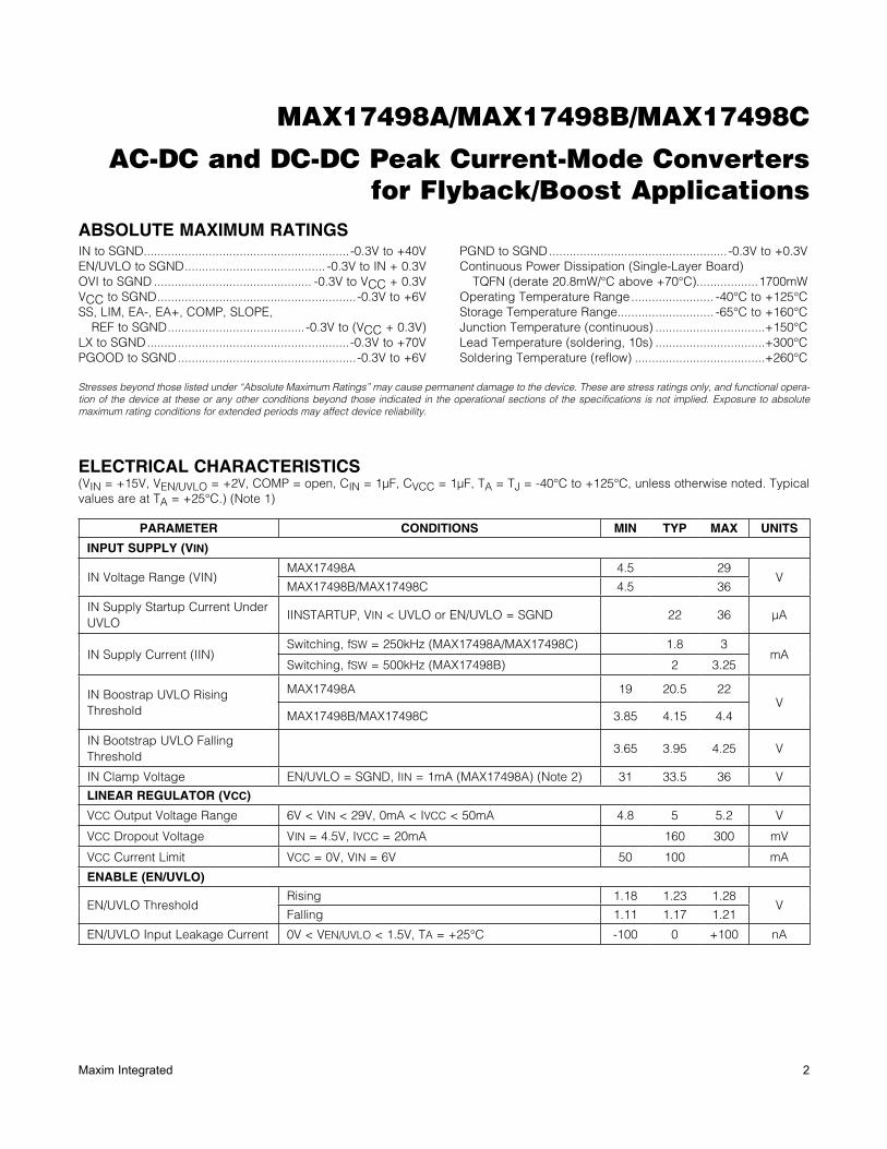
IN to SGND ............................................................-0.3V to +40VEN/UVLO to SGND ......................................... -0.3V to IN + 0.3VOVI to SGND .............................................. -0.3V to VCC + 0.3VVCC to SGND ..........................................................-0.3V to +6VSS, LIM, EA-, EA+, COMP, SLOPE,
REF to SGND ........................................-0.3V to (VCC + 0.3V)LX to SGND ...........................................................-0.3V to +70VPGOOD to SGND ....................................................-0.3V to +6V
PGND to SGND ....................................................-0.3V to +0.3VContinuous Power Dissipation (Single-Layer Board) TQFN (derate 20.8mW/°C above +70°C)..................1700mWOperating Temperature Range ........................ -40°C to +125°CStorage Temperature Range ............................ -65°C to +160°CJunction Temperature (continuous) ................................+150°CLead Temperature (soldering, 10s) ................................+300°CSoldering Temperature (reflow) ......................................+260°C
ABSOLUTE MAXIMUM RATINGS
Stresses beyond those listed under “Absolute Maximum Ratings” may cause permanent damage to the device. These are stress ratings only, and functional opera-tion of the device at these or any other conditions beyond those indicated in the operational sections of the specifications is not implied. Exposure to absolute maximum rating conditions for extended periods may affect device reliability.
ELECTRICAL CHARACTERISTICS(VIN = +15V, VEN/UVLO = +2V, COMP = open, CIN = 1µF, CVCC = 1µF, TA = TJ = -40°C to +125°C, unless otherwise noted. Typical values are at TA = +25°C.) (Note 1)
PARAMETER CONDITIONS MIN TYP MAX UNITS
INPUT SUPPLY (VIN)
IN Voltage Range (VIN)MAX17498A 4.5 29
VMAX17498B/MAX17498C 4.5 36
IN Supply Startup Current Under UVLO
IINSTARTUP, VIN < UVLO or EN/UVLO = SGND 22 36 µA
IN Supply Current (IIN)Switching, fSW = 250kHz (MAX17498A/MAX17498C) 1.8 3
mASwitching, fSW = 500kHz (MAX17498B) 2 3.25
IN Boostrap UVLO Rising Threshold
MAX17498A 19 20.5 22V
MAX17498B/MAX17498C 3.85 4.15 4.4
IN Bootstrap UVLO Falling Threshold
3.65 3.95 4.25 V
IN Clamp Voltage EN/UVLO = SGND, IIN = 1mA (MAX17498A) (Note 2) 31 33.5 36 V
LINEAR REGULATOR (VCC)
VCC Output Voltage Range 6V < VIN < 29V, 0mA < IVCC < 50mA 4.8 5 5.2 V
VCC Dropout Voltage VIN = 4.5V, IVCC = 20mA 160 300 mV
VCC Current Limit VCC = 0V, VIN = 6V 50 100 mA
ENABLE (EN/UVLO)
EN/UVLO ThresholdRising 1.18 1.23 1.28
VFalling 1.11 1.17 1.21
EN/UVLO Input Leakage Current 0V < VEN/UVLO < 1.5V, TA = +25NC -100 0 +100 nA
MAX17498A/MAX17498B/MAX17498C
AC-DC and DC-DC Peak Current-Mode Converters for Flyback/Boost Applications
3Maxim Integrated
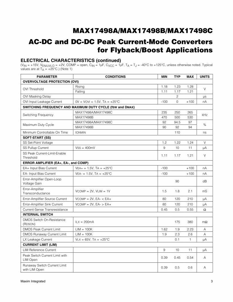
ELECTRICAL CHARACTERISTICS (continued)(VIN = +15V, VEN/UVLO = +2V, COMP = open, CIN = 1µF, CVCC = 1µF, TA = TJ = -40°C to +125°C, unless otherwise noted. Typical values are at TA = +25°C.) (Note 1)
PARAMETER CONDITIONS MIN TYP MAX UNITS
OVERVOLTAGE PROTECTION (OVI)
OVI ThresholdRising 1.18 1.23 1.28
VFalling 1.11 1.17 1.21
OVI Masking Delay 2 µs
OVI Input Leakage Current 0V < VOVI < 1.5V, TA = +25NC -100 0 +100 nA
SWITCHING FREQUENCY AND MAXIMUM DUTY CYCLE (fSW and DMAX)
Switching FrequencyMAX17498A/MAX17498C 235 250 265
kHzMAX17498B 470 500 530
Maximum Duty Cycle MAX17498A/MAX17498C 92 94.5 97
%MAX17498B 90 92 94
Minimum Controllable On Time tONMIN 110 ns
SOFT-START (SS)
SS Set-Point Voltage 1.2 1.22 1.24 V
SS Pullup Current VSS = 400mV 9 10 11 µA
SS Peak Current-Limit-Enable Threshold
1.11 1.17 1.21 V
ERROR AMPLIFIER (EA+, EA-, and COMP)
EA+ Input Bias Current VEA+ = 1.5V, TA = +25NC -100 +100 nA
EA- Input Bias Current VEA- = 1.5V, TA = +25NC -100 +100 nA
Error-Amplifier Open-Loop Voltage Gain
90 dB
Error-Amplifier Transconductance
VCOMP = 2V, VLIM = 1V 1.5 1.8 2.1 mS
Error-Amplifier Source Current VCOMP = 2V, EA- < EA+ 80 120 210 µA
Error-Amplifier Sink Current VCOMP = 2V, EA- > EA+ 80 120 210 µA
Current-Sense Transresistance 0.45 0.5 0.55 I
INTERNAL SWITCH
DMOS Switch On-Resistance (RDSON)
ILX = 200mA 175 380 mI
DMOS Peak Current Limit LIM = 100K 1.62 1.9 2.23 A
DMOS Runaway Current Limit LIM = 100K 1.9 2.3 2.6 A
LX Leakage Current VLX = 65V, TA = +25NC 0.1 1 µA
CURRENT LIMIT (LIM)
LIM Reference Current 9 10 11 µA
Peak Switch Current Limit with LIM Open
0.39 0.45 0.54 A
Runaway Switch Current Limit with LIM Open
0.39 0.5 0.6 A

MAX17498A/MAX17498B/MAX17498C
AC-DC and DC-DC Peak Current-Mode Converters for Flyback/Boost Applications
4Maxim Integrated
Note 1: All devices are 100% production tested at TA = +25NC. Limits over temperature are guaranteed by design.Note 2: The MAX17498A is intended for use in universal input power supplies. The internal clamp circuit at IN is used to prevent the
bootstrap capacitor from charging to a voltage beyond the absolute maximum rating of the device when EN/UVLO is low (shutdown mode). Externally limit the maximum current to IN (hence to clamp) to 2mA (max) when EN/UVLO is low.
ELECTRICAL CHARACTERISTICS (continued)(VIN = +15V, VEN/UVLO = +2V, COMP = open, CIN = 1µF, CVCC = 1µF, TA = TJ = -40°C to +125°C, unless otherwise noted. Typical values are at TA = +25°C.) (Note 1)
PARAMETER CONDITIONS MIN TYP MAX UNITS
Number of Runaway Current-Limit Hits Before Hiccup Timeout
1 #
Overcurrent Hiccup Timeout 32 ms
SLOPE COMPENSATION (SLOPE)
SLOPE Pullup Current 9 10 11 µA
SLOPE-Compensation Resistor Range
MAX17498B 30 150 kI
Default SLOPE-Compensation Ramp
SLOPE = open 60 mV/µs
POWER-GOOD SIGNAL (PGOOD)
PGOOD Output-Leakage Current (Off State)
VPGOOD = 5V, TA = +25NC -1 +1 µA
PGOOD Output Voltage (On State)
IPGOOD = 10mA 0 0.4 V
PGOOD Higher Threshold EA- rising 93.5 95 96.5 %
PGOOD Lower Threshold EA- falling 90.5 92 93.5 %
PGOOD Delay After EA- Reaches 95% Regulation
4 ms
THERMAL SHUTDOWN
Thermal-Shutdown Threshold Temperature rising +160 NC
Thermal-Shutdown Hysteresis 20 NC
MAX17498A/MAX17498B/MAX17498C
AC-DC and DC-DC Peak Current-Mode Converters for Flyback/Boost Applications
5Maxim Integrated
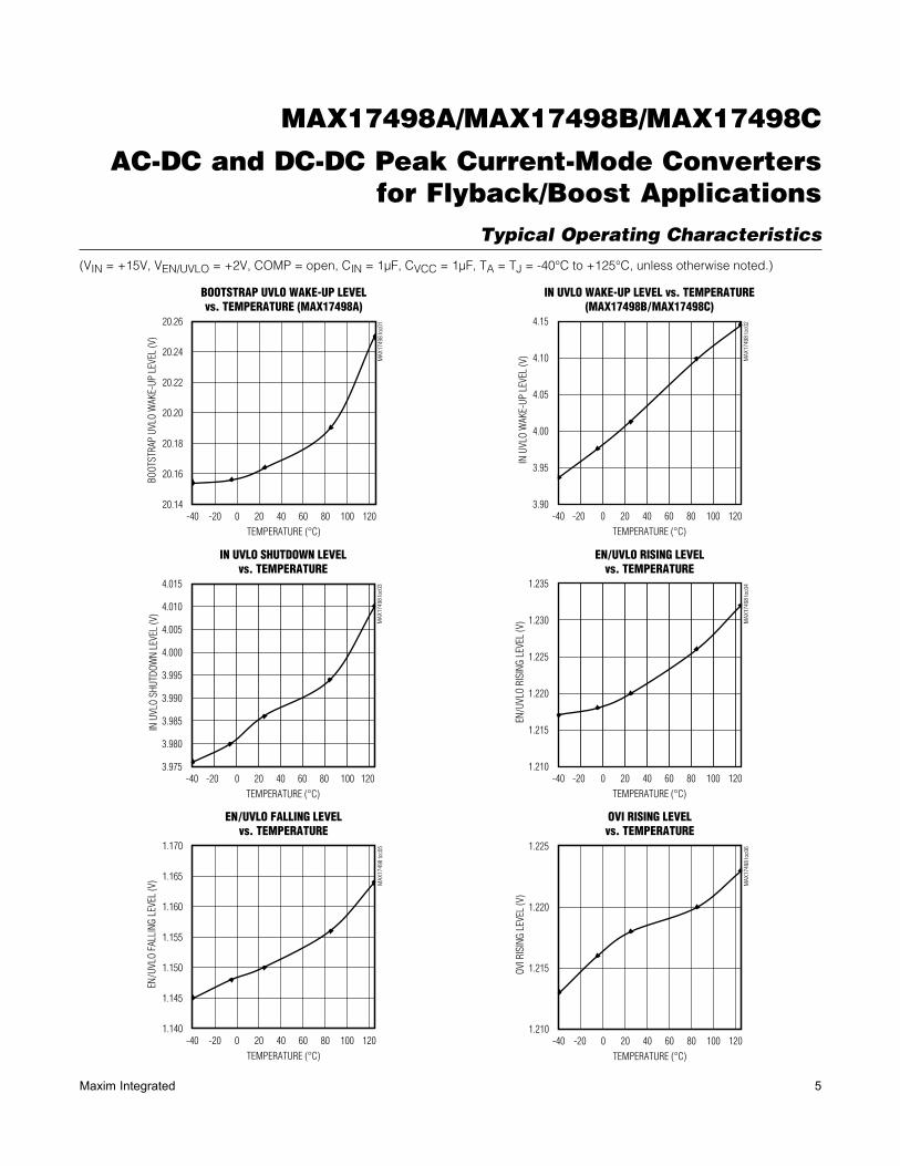
Typical Operating Characteristics
(VIN = +15V, VEN/UVLO = +2V, COMP = open, CIN = 1µF, CVCC = 1µF, TA = TJ = -40°C to +125°C, unless otherwise noted.)
BOOTSTRAP UVLO WAKE-UP LEVELvs. TEMPERATURE (MAX17498A)
MAX
1749
8 to
c01
TEMPERATURE (°C)
BOOT
STRA
P UV
LO W
AKE-
UP L
EVEL
(V)
120100806040200-20
20.16
20.18
20.20
20.22
20.24
20.26
20.14-40
IN UVLO SHUTDOWN LEVELvs. TEMPERATURE
MAX
1749
8 to
c03
IN U
VLO
SHUT
DOW
N LE
VEL
(V)
120100-20 0 20 6040 80
3.980
3.985
3.990
3.995
4.000
4.005
4.010
4.015
3.975-40
TEMPERATURE (°C)
EN/UVLO FALLING LEVELvs. TEMPERATURE
MAX
1749
8 to
c05
TEMPERATURE (°C)
EN/U
VLO
FALL
ING
LEVE
L (V
)
120100806040200-20
1.145
1.150
1.155
1.160
1.165
1.170
1.140-40
MAX
1749
8 to
c02
TEMPERATURE (°C)IN
UVL
O W
AKE-
UP L
EVEL
(V)
IN UVLO WAKE-UP LEVEL vs. TEMPERATURE(MAX17498B/MAX17498C)
3.95
4.00
4.05
4.10
4.15
3.90120100806040200-20-40
MAX
1749
8 to
c04
TEMPERATURE (°C)
EN/U
VLO
RISI
NG L
EVEL
(V)
EN/UVLO RISING LEVELvs. TEMPERATURE
1.215
1.220
1.225
1.230
1.235
1.210120100806040200-20-40
OVI RISING LEVELvs. TEMPERATURE
MAX
1749
8 to
c06
OVI R
ISIN
G LE
VEL
(V)
120100806040200-20
1.215
1.220
1.225
1.210-40
TEMPERATURE (°C)

MAX17498A/MAX17498B/MAX17498C
AC-DC and DC-DC Peak Current-Mode Converters for Flyback/Boost Applications
6Maxim Integrated
Typical Operating Characteristics (continued)
(VIN = +15V, VEN/UVLO = +2V, COMP = open, CIN = 1µF, CVCC = 1µF, TA = TJ = -40°C to +125°C, unless otherwise noted.)
MAX
1749
8 to
c07
TEMPERATURE (°C)
OVI F
ALLI
NG L
EVEL
(V)
OVI FALLING LEVELvs. TEMPERATURE
1.140
1.145
1.150
1.155
1.160
1.135120100806040200-20-40
IN CURRENT DURING SWITCHINGvs. TEMPERATURE
MAX
1749
8 to
c09
TEMPERATURE (°C)
IN C
URRE
NT D
URIN
G SW
ITCH
ING
(mA)
120100806040200-20
1.6
1.8
2.0
2.2
2.4
2.6
1.4-40
EN STARTUP WAVEFORMMAX17498 toc11
VCOMP1V/div
VOUT5V/div
EN/UVLO5V/div
400µs/div
MAX
1749
8 to
c08
TEMPERATURE (°C)
IN C
URRE
NT U
NDER
UVL
O (µ
A)
IN CURRENT UNDER UVLOvs. TEMPERATURE
22
24
26
28
30
20120100806040200-20-40
LX AND PRIMARY CURRENT WAVEFORMMAX17498 toc10
IPRI0.5A/div
VLX20V/div
1µs/div
EN SHUTDOWN WAVEFORMMAX17498 toc12
VCOMP1V/div
VOUT5V/div
EN/UVLO5V/div
400µs/div
MAX17498A/MAX17498B/MAX17498C
AC-DC and DC-DC Peak Current-Mode Converters for Flyback/Boost Applications
7Maxim Integrated
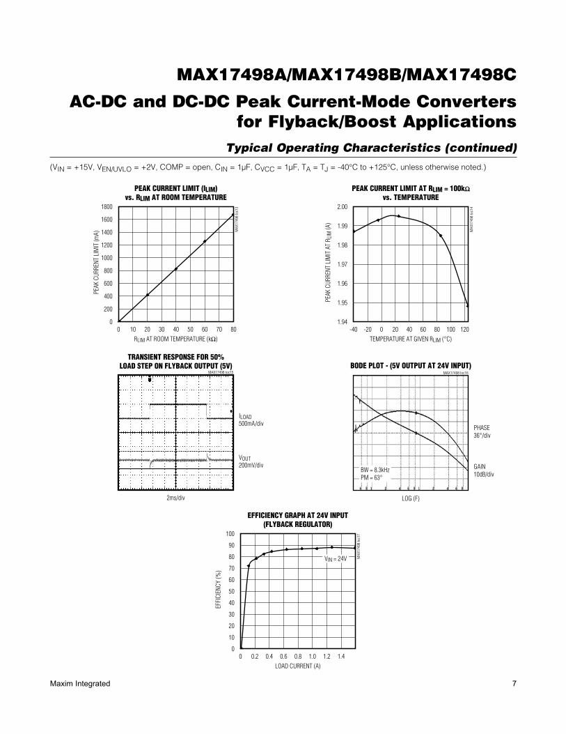
Typical Operating Characteristics (continued)
(VIN = +15V, VEN/UVLO = +2V, COMP = open, CIN = 1µF, CVCC = 1µF, TA = TJ = -40°C to +125°C, unless otherwise noted.)
PEAK CURRENT LIMIT (ILIM)vs. RLIM AT ROOM TEMPERATURE
MAX
1749
8 to
c13
RLIM AT ROOM TEMPERATURE (kI)
PEAK
CUR
RENT
LIM
IT (m
A)
706040 5020 3010
200
400
600
800
1000
1200
1400
1600
1800
00 80
TRANSIENT RESPONSE FOR 50%LOAD STEP ON FLYBACK OUTPUT (5V)
MAX17498 toc15
VOUT200mV/div
ILOAD500mA/div
2ms/div
LOAD CURRENT (A)
EFFI
CIEN
CY (%
)
1.41.20.8 1.00.4 0.60.20
EFFICIENCY GRAPH AT 24V INPUT(FLYBACK REGULATOR)
MAX
1749
8 to
c17
10
20
30
40
50
60
70
80
90
100
0
VIN = 24V
PEAK CURRENT LIMIT AT RLIM = 100kIvs. TEMPERATURE
MAX
1749
8 to
c14
TEMPERATURE AT GIVEN RLIM (°C)
PEAK
CUR
RENT
LIM
IT A
T R L
IM (A
)120100806040200-20
1.95
1.96
1.97
1.98
1.99
2.00
1.94-40
BODE PLOT - (5V OUTPUT AT 24V INPUT)MAX17498 toc16
GAIN10dB/div
PHASE36°/div
LOG (F)
BW = 8.3kHzPM = 63°
MAX17498A/MAX17498B/MAX17498C
AC-DC and DC-DC Peak Current-Mode Converters for Flyback/Boost Applications
8Maxim Integrated
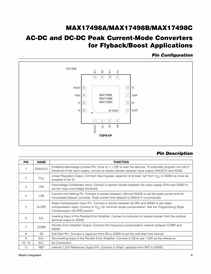
Pin Description
Pin Configuration
PIN NAME FUNCTION
1 EN/UVLOEnable/Undervoltage-Lockout Pin. Drive to > 1.23V to start the devices. To externally program the UVLO threshold of the input supply, connect a resistor-divider between input supply EN/UVLO and SGND.
2 VCCLinear Regulator Output. Connect input bypass capacitor of at least 1µF from VCC to SGND as close as possible to the IC.
3 OVIOvervoltage Comparator Input. Connect a resistor-divider between the input supply (OVI) and SGND to set the input overvoltage threshold.
4 LIMCurrent-Limit Setting Pin. Connect a resistor between LIM and SGND to set the peak-current limit for nonisolated flyback converter. Peak-current limit defaults to 500mA if unconnected.
5 SLOPESlope Compensation Input Pin. Connect a resistor between SLOPE and SGND to set slope- compensation ramp. Connect to VCC for minimum slope compensation. See the Programming Slope Compensation (SLOPE) section.
6 EA-Inverting Input of the Flexible Error Amplifier. Connect to mid-point of resistor-divider from the positive terminal output to SGND.
7 COMPFlexible Error-Amplifier Output. Connect the frequency-compensation network between COMP and SGND.
8 SS Soft-Start Pin. Connect a capacitor from SS to SGND to set the soft-start time interval.
9 EA+ Noninverting Input of the Flexible Error Amplifier. Connect to SS to use 1.22V as the reference.
10, 12 N.C. No Connection
11 REF Internal 1.22V Reference Output Pin. Connect a 100pF capacitor from REF to SGND.
15
16
14
13
6
5
7
V CC
LIM
8
EN/U
VLO
REF
EA+
N.C.
1 2
PGND
4
12 11 9
LX
EP (SGND)IN
SS
COMP
EA-
SLOPE+
OVI
N.C.
3
10
PGOOD
TQFN-EP
TOP VIEW
MAX17498AMAX17498BMAX17498C

MAX17498A/MAX17498B/MAX17498C
AC-DC and DC-DC Peak Current-Mode Converters for Flyback/Boost Applications
9Maxim Integrated
Pin Description (continued)
Detailed Description
The MAX17498A offers a bootstrap UVLO wakeup level of 20V with a wide hysteresis of 15V (min) optimized for implementing an isolated and nonisolated universal (85V AC to 265V AC) offline single-switch flyback converter or telecom (36V to 72V) power supplies. The MAX17498B/MAX17498C offer a UVLO wakeup level of 4.4V and are well suited for low-voltage DC-DC flyback/boost power supplies. An internal reference (1.22V) can be used to regulate the output down to 1.23V in nonisolated flyback and boost applications. Additional semi-regulated outputs, if needed, can be generated by using additional secondary windings on the flyback converter transformer. A flexible error amplifier and REF allow the end-user selection between regulating positive and negative outputs.
The devices utilize peak current-mode control and exter-nal compensation for optimizing the loop performance for various inductors and capacitors. The devices include a runaway current limit feature that triggers hiccup mode operation to protect the external component by halting switching for 32ms before restart. The devices include voltage soft-start for nonisolated designs and current soft-start for isolated designs to allow monotonic rise of the output voltage. The voltage or current soft-start can be selected using the SLOPE pin. See the Block Diagram for more information.
Input Voltage RangeThe MAX17498A has different rising and falling UVLO thresholds on the IN pin than those of the MAX17498B/MAX17498C. The thresholds for the MAX17498A are optimized for implementing power-supply startup schemes typically used for offline AC-DC power supplies.
The MAX17498A is therefore well suited for opera-tion from the rectified DC bus in AC-DC power-supply applications typically encountered in front-end industrial power-supply applications. As such, the MAX17498A has no limitation on the maximum input voltage as long as the external components are rated suitably and the maximum operating voltages of the MAX17498A are respected. The MAX17498A can successfully be used in universal input-rectified (85V to 265V AC) bus applica-tions, rectified 3-phase DC bus applications, and tele-com (36V to 72V DC) applications.
The MAX17498B/MAX17498C are intended for imple-menting a flyback (isolated and nonisolated) and boost converter with an on-board 65V rated n-channel MOSFET. The IN pin of the MAX17498B/MAX17498C has a maximum operating voltage of 36V. The MAX17498B/MAX17498C implement rising and falling thresholds on the IN pin that assume power-supply startup schemes, typical of lower voltage DC-DC applications, down to an input voltage of 4.5V DC. Therefore, flyback converters with a 4.5V to 36V supply voltage range can be imple-mented with the MAX17498B/MAX17498C.
Internal Linear Regulator (VCC)The internal functions and driver circuits are designed to operate from a 5V Q5% power-supply voltage. The devices have an internal linear regulator that is powered from the IN pin and generates a 5V power rail. The output of the linear regulator is connected to the VCC pin and should be decoupled with a 2.2µF capacitor to ground for stable operation. The VCC converter output supplies the operating current for the devices. The maximum operating voltage of the IN pin is 29V for the MAX17498A and 36V for the MAX17498B/MAX17498C.
PIN NAME FUNCTION
13 PGOODOpen-Drain Output. PGOOD goes high when EA- is within 5% of the set point. PGOOD pulls low when EA- falls below 92% of its set-point value.
14 PGND Power Ground for Converter
15 LX External Transformer/Inductor Connection for the Converter
16 INInternal Linear Regulator Input. Connect IN to the input-voltage source. Bypass IN to PGND with a 1µF (min) ceramic capacitor.
—EP
(SGND)Exposed Pad. Internally connected to SGND. Connect EP to a large copper plane at SGND potential to provide adequate thermal dissipation. Connect EP (SGND) to PGND at a single point.

MAX17498A/MAX17498B/MAX17498C
AC-DC and DC-DC Peak Current-Mode Converters for Flyback/Boost Applications
10Maxim Integrated
Configuring the Power Stage (LX)The devices use an internal n-channel MOSFET to imple-ment internal current sensing for current-mode control and overcurrent protection of the flyback/boost converter. To facilitate this, the drain of the internal nMOSFET is connect-ed to the source of the external MOSFET in the MAX17498A high-input-voltage applications. The gate of the external MOSFET is connected to the IN pin. Ensure by design that the IN pin voltage does not exceed the maximum operating gate-voltage rating of the external MOSFET. The external MOSFET gate-source voltage is controlled by the switch-ing action of the internal nMOSFET, while also sensing the source current of the external MOSFET. In the MAX17498B/MAX17498C-based applications, the LX pin is directly con-nected to either the flyback transformer primary winding or to the boost-converter inductor.
Maximum Duty CycleThe MAX17498A/MAX17498C operate at a maximum duty cycle of 94%. The MAX17498B offers a maximum duty cycle of 92%. The devices can be used to imple-ment flyback and boost converters involving large input-to-output voltage ratios in DC-DC applications.
Power-Good Signal (PGOOD)The devices include a PGOOD signal that serves as a power-good signal to the system. PGOOD is an open-drain signal and requires a pullup resistor to the preferred supply voltage. The PGOOD signal monitors EA- and pulls high when EA- is 95% (typ) of its regulation value (1.22V). For isolated power supplies, PGOOD can-not serve as a power-good signal.
Figure 1. MAX17498A/MAX17498B/MAX17498C Block Diagram
PEAK
RUNAWAY
PWM
CHIPEN
CONTROLLOGIC AND
DRIVER
CLK
VSUM
COMP
LIMINT
VCS
COMP
EA+
EA-
OSC
BGPOK
LDO33V CLAMP
(MAX17498A ONLY)
CHIPEN
1.23V
1.23V
1.23V
250mV
SLOPE
LIM
OVI
EN/UVLO
IN
SS
REF
VOLTAGE SS
CURRENT SS
SSDONE
SSDONE
VCC 5V, 50mA
10µA
DECODER
VOLTAGE SS CURRENT SS
FIXED SLOPE
VARIABLE SLOPE
10µA
PGOOD
BLOCK
PGOOD
EA-
1 RUNAWAY
PGND
LX
VCSVSLOPE
VSUM
SSDONE
SSDONEF
1.17V
CHIPEN
HICCUPSS
MAX17498AMAX17498BMAX17498C
10µA

MAX17498A/MAX17498B/MAX17498C
AC-DC and DC-DC Peak Current-Mode Converters for Flyback/Boost Applications
11Maxim Integrated
Soft-StartThe devices implement soft-start operation for the flyback /boost converter. A capacitor connected to the SS pin programs the soft-start period for the flyback/boost converter. The soft-start feature reduces the input inrush current. These devices allow the end user to select between voltage soft-start usually preferred in nonisolat-ed applications and current soft-start, which is useful in isolated applications to get a monotonic rise in the output voltage. See the Programming Soft-Start of the Flyback/Boost Converter (SS) section.
Spread-Spectrum Factory OptionFor EMI-sensitive applications, a spread-spectrum-enabled version of the device can be requested from the factory. The frequency-dithering feature modulates the switching frequency by Q10% at a rate of 4kHz. This spread-spectrum-modulation technique spreads the energy of switching-frequency harmonics over a wider band while reducing their peaks, helping to meet stringent EMI goals.
Applications Information
Startup Voltage and Input Overvoltage- Protection Setting (EN/UVLO, OVI)
The devices’ EN/UVLO pin serves as an enable /disable input, as well as an accurate programmable input UVLO pin. The devices do not commence startup operation unless the EN/UVLO pin voltage exceeds 1.23V (typ). The devices turn off if the EN/UVLO pin voltage falls below 1.17V (typ). A resistor-divider from the input DC bus to ground can be used to divide down and apply a fraction of the input DC voltage (VDC) to the EN/UVLO pin. The values of the resistor-divider can be selected so that the EN/UVLO pin voltage exceeds the 1.23V (typ) turn-on threshold at the desired input DC bus voltage. The same resistor-divider can be modified with an additional resistor (ROVI) to implement input overvoltage protection in addition to the EN/UVLO functionality as shown in Figure 2. When voltage at the OVI pin exceeds 1.23V (typ), the devices stop switching and resume switching opera-tions only if voltage at the OVI pin falls below 1.17V (typ). For given values of startup DC input voltage (VSTART), and input overvoltage-protection voltage (VOVI), the
resistor values for the divider can be calculated as fol-lows, assuming a 24.9kI resistor for ROVI:
OVIEN OVI
START
VR R 1 k
V
= × − Ω
where ROVI is in kI while VSTART and VOVI are in volts.
STARTSUM OVI EN
VR R R 1 k
1.23 = + × − Ω
where REN and ROVI are in kI. In universal AC input applications, RSUM might need to be implemented as equal resistors in series (RDC1, RDC2, RDC3) so that voltage across each resistor is limited to its maximum operation voltage.
SUMDC1 DC2 DC3
RR R R k
3= = = Ω
For low-voltage DC-DC applications based on the MAX17498B/MAX17498C, a single resistor can be used in the place of RSUM, as the voltage across it is approximately 40V.
Figure 2. Programming EN/UVLO and OVI
OVI
ROVI
REN
RSUM
VDC
RDC3
RDC2
RDC1
EN/UVLOMAX17498AMAX17498BMAX17498C

MAX17498A/MAX17498B/MAX17498C
AC-DC and DC-DC Peak Current-Mode Converters for Flyback/Boost Applications
12Maxim Integrated
Startup OperationThe MAX17498A is optimized for implementing an offline single-switch flyback converter and has a 20V IN UVLO wake-up level with hysteresis of 15V (min). In offline appli-cations, a simple cost-effective RC startup circuit is used. When the input DC voltage is applied, the startup resis-tor (RSTART) charges the startup capacitor (CSTART), causing the voltage at the IN pin to increase towards the wake-up IN UVLO threshold (20V typ). During this time, the MAX17498A draws a low startup current of 20µA (typ) through RSTART. When the voltage at IN reaches the wake-up IN UVLO threshold, the MAX17498A com-mences switching operations and drives the internal n-channel MOSFET whose drain is connected to the LX pin. In this condition, the MAX17498A draws 1.8mA cur-rent from CSTART, in addition to the current required to switch the gate of the external nMOSFET. Since this cur-rent cannot be supported by the current through RSTART, the voltage on CSTART starts to drop. When suitably con-figured, as shown in Figure 10, the external nMOSFET is switched by the LX pin and the flyback converter gener-ates pulses in bias winding NB. The soft-start period of the converter should be programmed so the bias winding pulses sustain the voltage on CSTART before it falls below 5V, thus allowing continued operation. The large hystere-sis (15V typ) of the MAX17498A allows for a small startup capacitor (CSTART). The low startup curent (20µA typ) allows the use of a large start resistor (RSTART), thus reduc-ing power dissipation at higher DC bus voltages. Figure 3 shows the typical RC startup scheme for the MAX17498A. RSTART might need to be implemented as equal, multiple
resistors in series (RIN1, RIN2, and RIN3) to share the applied high DC voltage in offline applications so that the voltage across each resistor is limited to the maximum continuous operating-voltage rating. RSTART and CSTART can be calculated as:
× × ×= + × × + µ
SS G sw
START VCC IN SS 60.04 t Q f
C 0.75 C I t 0.1 F10
where IIN is the supply current drawn at the IN pin in mA, QG is the gate charge of the external nMOSFET in nC, fSW is the switching frequency of the converter in Hz, and tSS is the soft-start time programmed for the flyback converter in ms. CVCC is the cummulative capacitor used in VCC node. See the Programming Soft-Start of the Flyback/Boost Converter (SS) section.
( )STARTSTART
START
V 10 50R k
1 C
− ×= Ω
+
where CSTART is the startup capacitor in µF.
For designs that cannot accept power dissipation in the startup resistors at high DC input voltages in offline appli-cations, the startup circuit can be set up with a current source instead of a startup resistor as shown in Figure 4.
Figure 3. MAX17498A RC-Based Startup Circuit Figure 4. MAX17498A Current Source-Based Startup Circuit
RSTART
RIN3
VDC
VDC VOUT
IN LX
VCC
CVCCCSTART
D1
RIN2
RIN1
COUT
MAX17498A
LDO
D2
NB NP NS
RSTART
RIN3
RISRC
IN
VDC
VDC VOUT
D1
IN
D2
LX
VCC
CVCC
CSTART
RIN2
RIN1
COUT
MAX17498A
LDO
NB NP NS
MAX17498A/MAX17498B/MAX17498C
AC-DC and DC-DC Peak Current-Mode Converters for Flyback/Boost Applications
13Maxim Integrated
Resistors RSUM and RISRC can be calculated as:
STARTSUM
BEQ1ISRC
VR M
10V
R M70
= Ω
= Ω
The IN UVLO wakeup threshold of the MAX17498B/MAX17498C is set to 3.9V (typ) with a 200mV hyster-esis, optimized for low-voltage DC-DC applications down to 4.5V. For applications where the input DC voltage is low enough (e.g., 4.5V to 5.5V DC) that the power loss incurred to supply the operating current of
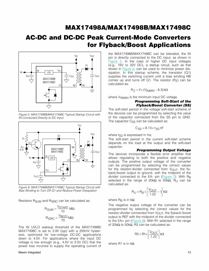
the MAX17498B/MAX17498C can be tolerated, the IN pin is directly connected to the DC input, as shown in Figure 5. In the case of higher DC input voltages (e.g., 16V to 32V DC), a startup circuit, such as that shown in Figure 6, can be used to minimize power dis-sipation. In this startup scheme, the transistor (Q1) supplies the switching current until a bias winding NB comes up and turns off Q1. The resistor (RZ) can be calculated as:
= × − ΩZ INMINR 2 (V 6.3)k
where VINMIN is the minimum input DC voltage.Programming Soft-Start of the Flyback/Boost Converter (SS)
The soft-start period in the voltage soft-start scheme of the devices can be programmed by selecting the value of the capacitor connected from the SS pin to GND. The capacitor CSS can be calculated as:
SS SSC 8.13 t nF= ×
where tSS is expressed in ms.The soft-start period in the current soft-start scheme depends on the load at the output and the soft-start capacitor.
Programming Output VoltageThe devices incorporate a flexible error amplifier that allows regulating to both the positive and negative outputs. The positive output voltage of the converter can be programmed by selecting the correct values for the resistor-divider connected from VOUT, the fly-back /boost output to ground, with the midpoint of the divider connected to the EA- pin (Figure 7). With RB selected in the range of 20kI to 50kI, RU can be calculated as:
OUTU B
VR R 1 k
1.22 = × − Ω
where RB is in kI.
The negative output voltage of the converter can be programmed by selecting the correct values for the resistor-divider connected from VOUT, the flyback /boost output to REF with the midpoint of the divider connected to the EA+ pin (Figure 8). With R1 selected in the range of 20kI to 50kI, R2 can be calculated as:
OUTVR2 R1 k
1.22 = × Ω
where R1 is in kI.
Figure 5. MAX17498B/MAX17498C Typical Startup Circuit with IN Connected Directly to DC Input
Figure 6. MAX17498B/MAX17498C Typical Startup Circuit with Bias Winding to Turn Off Q1 and Reduce Power Dissipation
VDC VOUT
IN
LX Np Ns
VCCIN
D1
CIN COUTCVCCMAX17498BMAX17498C
LDO
VDC
VOUT
LX Np NsIN
COUT
MAX17498BMAX17498C
IN
NB
VCC
CVCC
CIN
D2
D1RZ
ZD16.3V
LDO
Q1

MAX17498A/MAX17498B/MAX17498C
AC-DC and DC-DC Peak Current-Mode Converters for Flyback/Boost Applications
14Maxim Integrated
Current-Limit Programming (LIM)The devices include a robust overcurrent-protection scheme that protects the device under overload and short-circuit conditions. For the flyback/boost con-verter, the devices include a cycle-by-cycle peak current limit that turns off the driver whenever the current into the LX pin exceeds an internal limit that is programmed by the resistor connected from the LIM pin to GND. The devices include a runaway current limit that protects the device under short-circuit conditions. One occurrence of the runaway current limit triggers a hiccup mode that protects the converter by immediately suspending switching for a period of time (32ms). This allows the overload current to decay due to power loss in the converter resistances, load, and the output diode of the flyback/boost converter before soft-start is attempted again. The resistor at the LIM pin for a desired current limit (IPK) can be calculated as:
LIM PKR 50 I k= × Ω
where IPK is expressed in amperes.
For a given peak current-limit setting, the runaway current limit is typically 20% higher. The runaway current-limit-triggered hiccup operation is always enabled even during soft-start.
Programming Slope Compensation (SLOPE)When the MAX17498A//MAX17498B/MAX17498C devic-es operate at a maximum duty cycle of 49%, in theory they do not require slope compensation for preventing subharmonic instability that occurs naturally in continu-ous-mode peak current-mode-controlled converters. In practice, the devices require a minimum amount of slope compensation to provide stable, jitter-free operation. These devices allow the user to program this default value of slope compensation simply by connecting the SLOPE pin to VCC. It is recommended that discontinuous-mode designs also use this minimum amount of slope compen-sation to provide noise immunity and jitter-free operation.
To avoid subharmonic instability that occurs naturally over all specified load and line conditions in peak cur-
rent-mode-controlled converters operating at duty cycles greater than 50%, the converter needs slope compen-sation. A minimum amount of slope signal is added to the sensed current signal even for converters operating below 50% duty to provide stable, jitter-free operation. The SLOPE pin allows the user to program the necessary slope compensation by setting the value of the resistor (RSLOPE) connected from SLOPE pin to ground.
SLOPE ER 0.5 S k= × Ω
where the slope (SE) is expressed in millivolts per micro-second.
Figure 7. Programming the Positive Output Voltage
Figure 8. Programming the Negative Output Voltage
RB
RU
EA-
VOUT
MAX17498AMAX17498BMAX17498C
R1
REA- EA+
EA-
REF
R2
VOUT
MAX17498AMAX17498BMAX17498C

MAX17498A/MAX17498B/MAX17498C
AC-DC and DC-DC Peak Current-Mode Converters for Flyback/Boost Applications
15Maxim Integrated
Thermal ConsiderationsIt should be ensured that the junction temperature of the devices does not exceed +125°C under the operating con-ditions specified for the power supply. The power dissipat-ed in the devices to operate can be calculated using the following equation:
IN IN INP V I= ×
where VIN is the voltage applied at the IN pin and IIN is operating supply current.
The internal n-channel MOSFET experiences conduction loss and transition loss when switching between on and off states. These losses are calculated as:
( )
2CONDUCTION LXRMS DSONLX
TRANSITION INMAX PK R F SW
P I R
P 0.5 V I t t f
= ×
= × × × + ×
where tR and tF are the rise and fall times of the internal nMOSFET in CCM operation. In DCM operation, since the switch current starts from zero, only tF exists and the transition-loss equation changes to:
TRANSITION INMAX PK F SWP 0.5 V I t f= × × × ×
Additional loss occurs in the system in every switch-ing cycle due to energy stored in the drain-source capacitance of the internal MOSFET being lost when the MOSFET turns on and discharges the drain-source capacitance voltage to zero. This loss is estimated as:
CAP DS DSMAX SWP 0.5 C V f= × × ×
The total power loss in the devices can be calculated from the following equation:
LOSS IN CONDUCTION TRANSITION CAPP P P P P= + + +
The maximum power that can be dissipated in the devices is 1666mW at +70°C temperature. The power-dissipation capability should be derated as the tem-perature rises above +70°C at 21mW/°C. For a multilayer board, the thermal-performance metrics for the package are given below:
JA
JC
48°C / W
10°C / W
θ =
θ =
The junction-temperature rise of the devices can be estimated at any given maximum ambient temperature (TAMAX) from the following equation:
( )JMAX AMAX JA LOSST T P= + θ ×
If the application has a thermal-management system that ensures that the exposed pad of the devices is maintained at a given temperature (TEPMAX) by using proper heatsinks, then the junction-temperature rise of the devices can be estimated at any given maximum ambient temperature from the following equation:
( )üüüüüüüT T P= + θ ×
Layout, Grounding, and BypassingAll connections carrying pulsed currents must be very short and as wide as possible. The inductance of these connections must be kept to an absolute minimum due to the high di/dt of the currents in high-frequency switching power converters. This implies that the loop areas for forward and return pulsed currents in various parts of the circuit should be minimized. Additionally, small-current loop areas reduce radiated EMI. Similarly, the heatsink of the main MOSFET presents a dV/dt source, and therefore, the surface area of the MOSFET heatsink should be minimized as much as possible.
Ground planes must be kept as intact as possible. The ground plane for the power section of the converter should be kept separate from the analog ground plane, except for a connection at the least noisy section of the power ground plane, typically the return of the input filter capacitor. The negative terminal of the filter capacitor, ground return of the power switch, and current-sensing resistor must be close together. PCB layout also affects the thermal performance of the design. A number of ther-mal vias that connect to a large ground plane should be provided under the exposed pad of the part for efficient heat dissipation. For a sample layout that ensures first-pass success, refer to the MAX17498B Evaluation Kit.
For universal AC input designs, follow all applicable safety regulations. Offline power supplies can require UL, VDE, and other similar agency approvals.
MAX17498A/MAX17498B/MAX17498C
AC-DC and DC-DC Peak Current-Mode Converters for Flyback/Boost Applications
16Maxim Integrated
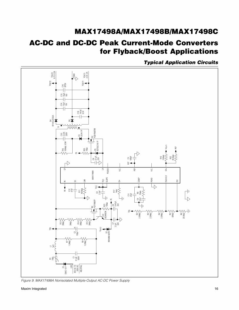
Figure 9. MAX17498A Nonisolated Multiple-Output AC-DC Power Supply
Typical Application Circuits
PGOO
D
N.C.
N.C.
PGND
ININ
EP
LIM
SS
R11
49.9
kIC12
47nF
V CC
SLOP
E
V CC
C4 2.2µ
F
R582
kI R620
.5kI
EN/U
VLO
OVI
R42.
2MIR3
2.2M
IR22.
2MI
V IN
R15
3MI
R14
3MI
3MI
R12
3MI
INC6 0.
47µF
,35
V
R23
10kI
N2 FQT1
N80T
F
C72.
2µF,
50V
V OUT
2
Q1BC
849C
WD2
RB16
0M-6
0TR
V IN
C210
0µF
L1 1µH
R81.
2MI
C10.
1µF,
630V
D1S5
KC-1
3-F
LINE
NEUT
RAL
85V
AC T
O26
5V A
C
R71.
2MI
R1 10I
LX
D4RF
101L
2STE
25
D3 US1K
-TP
D5 BZT5
2C18
-7F
N1 FQD1
N80T
MC8 0.
1µF,
25V
C18
141µ
F,6.
3V
D6
C14
10µF
,16
V
C15
10µF
,16
V
C10
2.2n
F,25
0V
R16
100kI
, 0.5
W
R20
10I
T1
C16
OPENV O
UT2
IN
V OUT
1V O
UT1
-3.3
V, 2
A
V OUT
28.
7V, 0
.3A
PGND
MAX17498A
C310
0pF
REF
REF
V OUT
1EA
+
R10
133kI
R22
49.3
kIRE
F
EA-
R17
1kI
COM
PC9 22
nF
C11
47pF R9 15
kI

MAX17498A/MAX17498B/MAX17498C
AC-DC and DC-DC Peak Current-Mode Converters for Flyback/Boost Applications
17Maxim Integrated
Figure 10. MAX17498B Isolated DC-DC Power Supply
PGND
PGOOD
C44.7µF, 50V
C50.22µF, 50V
REF
EA+
SS
R420kI
OVI
PGND
EN/UVLO
R510kI
EN/UVLO
OVI
R3348kI
VIN
VFB
VIN
C147µF,
63V
18V TO 36VINPUT
PGND
VIN
C24.7µF,
50V
IN
U1
C968nF
LX
D2
D1
C1222µF,16V
C1322µF,16V
C333nF
R17.5kI
T1
C1422µF,16V
5V, 1.5AOUTPUT
VOUT
VOUT
GND
MAX17498B
C62.2µF, 16V
VCC
VCC
REF C10100pF
REF
LIM
R686.6kI
R910kI
R1115kI
COMP
EA-
SLOPE
R70I
PGOOD
R1210kI
VCC
VCC R151kI
R2030.3kI
R1910kI
C154.7nF
R1815kI C16
33pF
12
3U3
C18OPEN
R13511I
U2
VFB
VOUT

MAX17498A/MAX17498B/MAX17498C
AC-DC and DC-DC Peak Current-Mode Converters for Flyback/Boost Applications
18Maxim Integrated
Figure 11. MAX17498B Boost Power Supply
N.C.
N.C.
PGND
IN
SLOPE
VCC
R7OPEN
R80I
EN/UVLO
OVI
R60I
VIN
VIN
VIN
PGND
C71µF
C110µF
4.5V TO10V DC
MAX17498B
C8100pF
REF
REF
SS
EA+
EP
LX
IN
D1VOUT
24V, 0.1A
C62.2µF, 50V
L156µH
PGOODR9
10kIVCC
PGOOD
LIM
SS
R271.5kI
C547nF
SS
R212kI
C22.2µF
VCC
EA-
R3374kI
R420kI
VOUT
COMP
R52.73kI
C4270pF
C3100nF

MAX17498A/MAX17498B/MAX17498C
AC-DC and DC-DC Peak Current-Mode Converters for Flyback/Boost Applications
19Maxim Integrated
Package Information
For the latest package outline information and land patterns (footprints), go to www.maximintegrated.com/packages. Note that a “+”, “#”, or “-” in the package code indicates RoHS status only. Package drawings may show a different suffix character, but the drawing pertains to the package regardless of RoHS status.
Ordering Information
+Denotes a lead(Pb)-free/RoHS-compliant package.*EP = Exposed pad.
PART TEMP RANGE PIN-PACKAGE DESCRIPTION
MAX17498AATE+ -40°C to +125°C 16 TQFN-EP* 250kHz, Offline Flyback Converter
MAX17498BATE+ -40°C to +125°C 16 TQFN-EP* 500kHz, Low-Voltage DC-DC Flyback/Boost Converter
MAX17498CATE+ -40°C to +125°C 16 TQFN-EP* 250kHz, Low-Voltage DC-DC Flyback Converter
PACKAGE TYPE PACKAGE CODE OUTLINE NO. LAND PATTERN NO.
16 TQFN-EP T1633+5 21-0136 90-0032

MAX17498A/MAX17498B/MAX17498C
AC-DC and DC-DC Peak Current-Mode Converters for Flyback/Boost Applications
Maxim Integrated cannot assume responsibility for use of any circuitry other than circuitry entirely embodied in a Maxim Integrated product. No circuit patent licenses are implied. Maxim Integrated reserves the right to change the circuitry and specifications without notice at any time. The parametric values (min and max limits) shown in the Electrical Characteristics table are guaranteed. Other parametric values quoted in this data sheet are provided for guidance.
Maxim Integrated 160 Rio Robles, San Jose, CA 95134 USA 1-408-601-1000 20© 2013 Maxim Integrated Products, Inc. Maxim Integrated and the Maxim Integrated logo are trademarks of Maxim Integrated Products, Inc.
Revision History
REVISIONNUMBER
REVISIONDATE
DESCRIPTIONPAGES
CHANGED
0 9/11 Initial release —
1 3/12 Removed future product references for MAX17498B and MAX17498C 27
2 2/13
Changed the maximum duty cycle for the A/C variants to 92% (min), 94.5% (typ), and 97% (max); updated General Description, Benefits and Features, Detailed Description, Maximum Duty Cycle, Current-Limit Programming (LIM), Programming Slope Compensation (SLOPE), and Peak/RMS-Current Calculation secondary RMS current equation
1, 3, 9, 10, 14, 15
3 4/13Updated Benefits and Features, removed sections on pages 15–21, updated Figures 1, 3–6, 11, 12
1, 10, 12, 13, 15–22, 24, 25