material technologies for 3d semiconductor packaging 3d ic... · gap between 1st daf and substrate...
TRANSCRIPT

Material Technologies for 3D Semiconductor Packaging
Itsuo Watanabe, Ph.D.Hitachi Chemical Co., Ltd.
2Outline1.Trend of Semiconductor Packaging and
Technological Strategy for 3D Semiconductor Packaging Materials
2. Material Technologies • Stacked-CSP -DAF ( Die attach film)• PoP (Package on package) -Low CTE substrate • TSV (Through Silicon Via)
- Low Temperature Curable Dielectric Material- Underfill Materials (CUF, NCP, NCF)- Temporary Bonding Materials
3. Conclusion
3Outline1.Trend of Semiconductor Packaging and
Technological Strategy for 3D Semiconductor Packaging Materials
2. Material Technologies • Stacked-CSP -DAF ( Die attach film)• PoP (Package on package) -Low CTE substrate • TSV (Through Silicon Via)
- Low Temperature Curable Dielectric Material- Underfill Materials (CUF, NCP, NCF)- Temporary Bonding Materials
3. Conclusion

4
P-BGA
Redistributed chip PKG
Coreless PKG
WL-CSPFC-DDR
Flip Chip BGA
BOC
PoP Embedded
Stacked CSP TSV PKG
Chip on chip PKG
3DPackages
Logic (MPU, GPU)
Memory (DRAM, Flash)
Logic/Memory
Semiconductor package trend

5
3D packages and related materials
Molding compoundNCF, NCPDielectricCMP slurryTemporary bonding material
SubstrateMolding compoundDie attach filmCUF
SubstrateMolding compoundDie attach film
TSVThrough-Si-Via
PoPPackage-on-Package
Stacked-CSP
Requirements: High process ability, High reliability
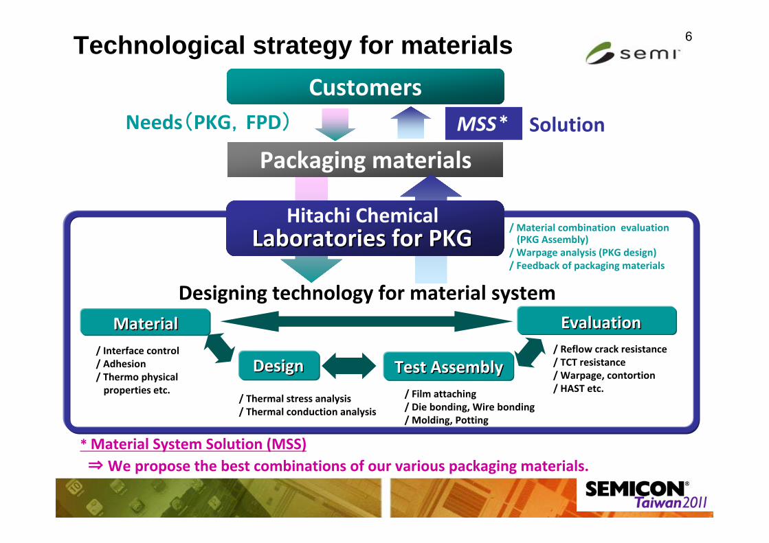
6Technological strategy for materials
MSS*
Designing technology for material system
Customers
Packaging materials
MaterialMaterial
DesignDesign Test AssemblyTest Assembly
EvaluationEvaluation
Hitachi Chemical Laboratories for PKG Laboratories for PKG
Needs(PKG,FPD)
/ Interface control/ Adhesion/ Thermo physicalproperties etc.
/ Thermal stress analysis/ Thermal conduction analysis
/ Film attaching/ Die bonding, Wire bonding / Molding, Potting
/ Reflow crack resistance/ TCT resistance/ Warpage, contortion / HAST etc.
Solution
/ Material combination evaluation (PKG Assembly)
/ Warpage analysis (PKG design)/ Feedback of packaging materials
* Material System Solution (MSS)⇒We propose the best combinations of our various packaging materials.
7Outline1.Trend of Semiconductor Packaging and
Technological Strategy for 3D Semiconductor Packaging Materials
2. Material Technologies • Stacked-CSP -DAF ( Die attach film)• PoP (Package on package) -Low CTE substrate • TSV (Through Silicon Via)
- Low Temperature Curable Dielectric Material- Underfill Materials (CUF, NCP, NCF)- Temporary Bonding Materials
3. Conclusion

8Trend of stacked-CSP and requirements
Pyramid type
Spacer type
Wire Penetration type
Die Shift type
•No voids•MSL reliability
2012 20142008 2010 20162006200420022000300-150µm 100-50µm150-100µm 25-50µm
•No voids•MSL reliability•Low viscosity at molding
•No voids•MSL reliability

9
Process flow of stacked-CSP and requirements
MountingPick-upDicing
•No kerf•Thinned wafer handling•Two in one process
•No chip crack •No voids
Collet
Needle
10
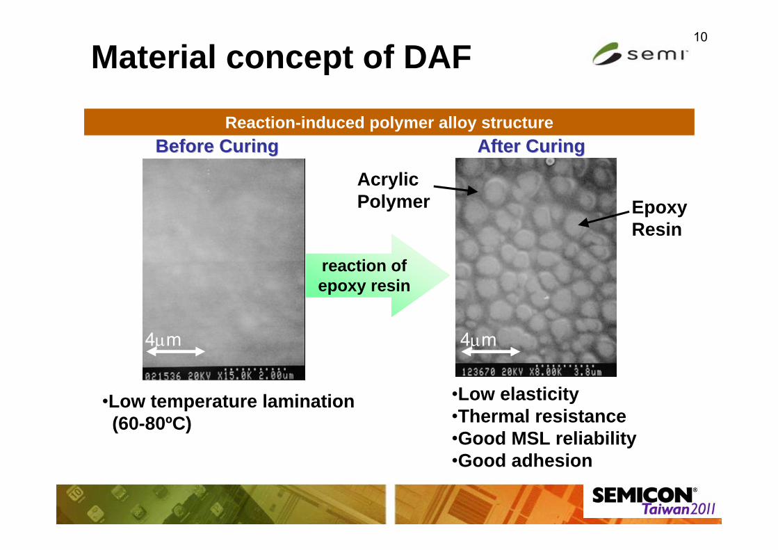
Material concept of DAF
Before CuringBefore Curing
Acrylic Polymer
•Low elasticity•Thermal resistance•Good MSL reliability•Good adhesion
After CuringAfter Curing
•Low temperature lamination(60-80ºC)
4m
Reaction of Epoxy Resin
4m
Reaction-induced polymer alloy structure
reaction ofepoxy resin
Epoxy Resin
11
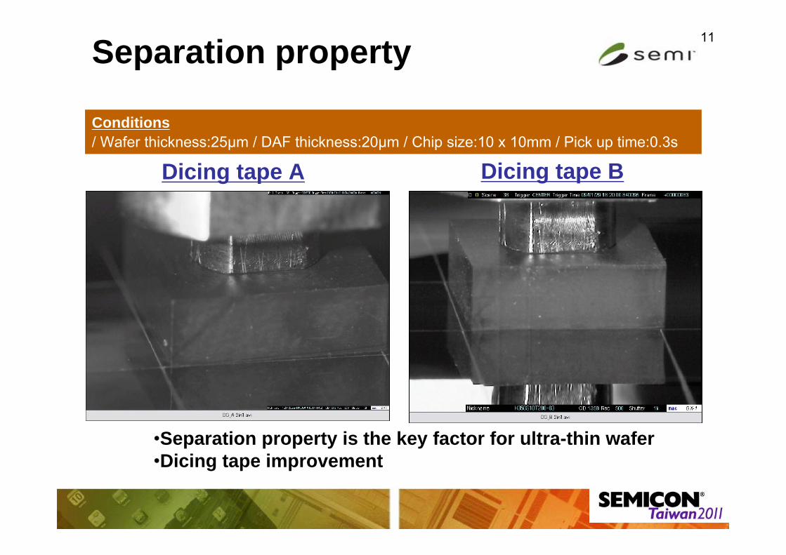
Conditions/ Wafer thickness:25µm / DAF thickness:20µm / Chip size:10 x 10mm / Pick up time:0.3s
Dicing tape A Dicing tape B
Separation property
•Separation property is the key factor for ultra-thin wafer•Dicing tape improvement
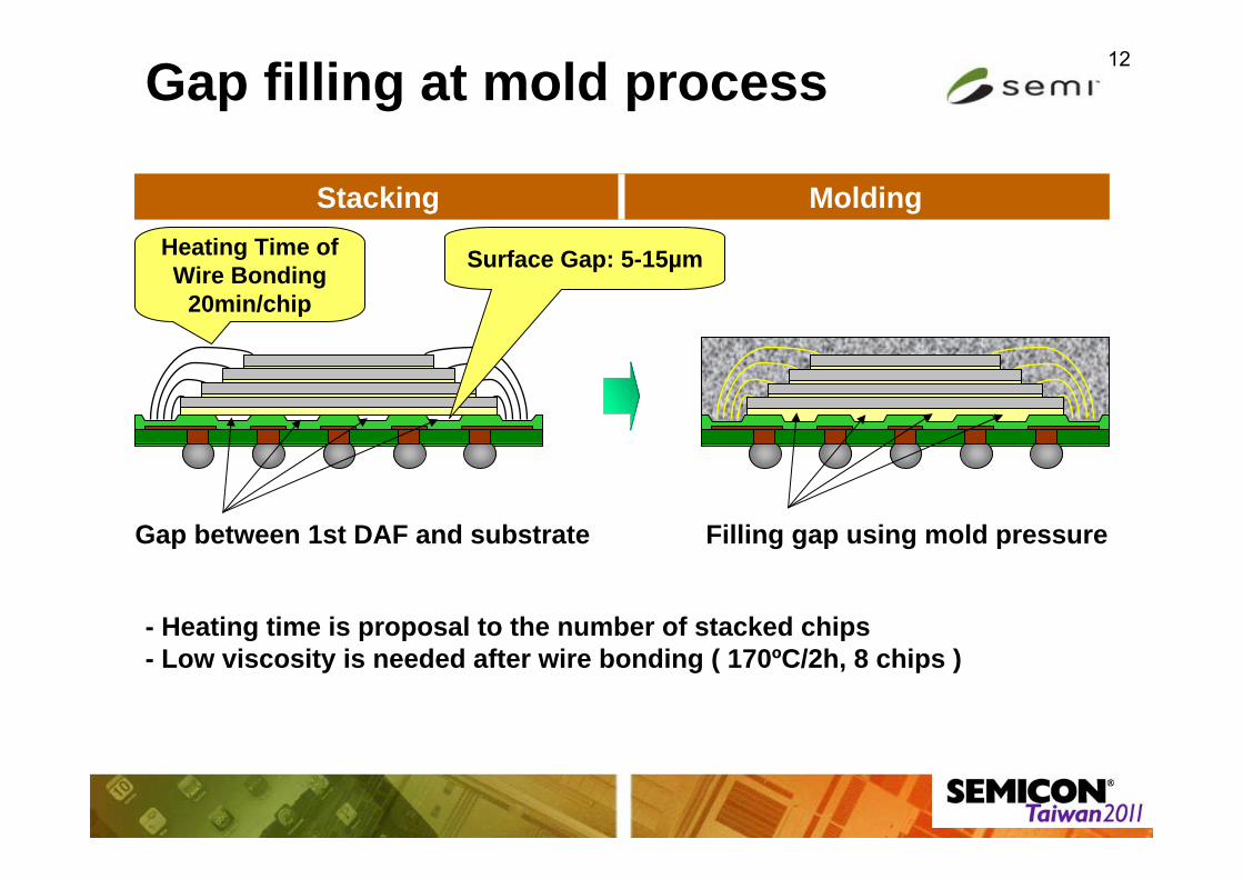
12Gap filling at mold process
Gap between 1st DAF and substrate Filling gap using mold pressure
MoldingStacking
Surface Gap: 5-15µmHeating Time ofWire Bonding
20min/chip
- Heating time is proposal to the number of stacked chips- Low viscosity is needed after wire bonding ( 170ºC/2h, 8 chips )
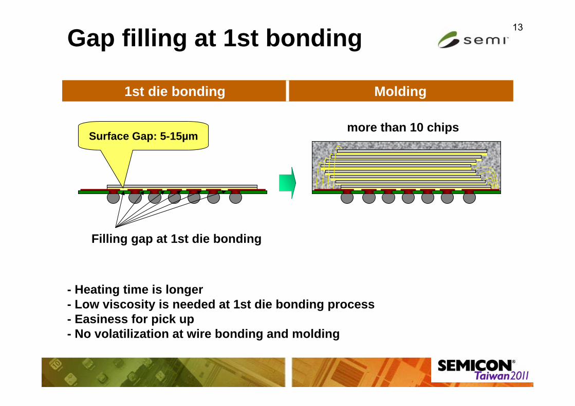
13Gap filling at 1st bonding
Molding1st die bonding
Filling gap at 1st die bonding
Surface Gap: 5-15µm
- Heating time is longer- Low viscosity is needed at 1st die bonding process- Easiness for pick up- No volatilization at wire bonding and molding
more than 10 chips

14
High gap filling capability
Wire penetrationHigh fluidity film
Multi chip stackedMulti chip stackedGap filling at Mold process
Higher fluidity film
Void free
*Gap filling is done at D/A process
Technology platform of DAF
High Filler &Epoxy content
Polymer Rich Viscosity control
Blade Dicing
- Lower burr generation- Easy pick-up- High modulus at W/B
- Stealth DC process- Laser full cut process- DBG + Laser full cut
Laser DicingThinner WaferThinner Wafer
DC tape improvement DC tape improvement

15Outline1.Trend of Semiconductor Packaging and
Technological Strategy for 3D Semiconductor Packaging Materials
2. Material Technologies • Stacked-CSP -DAF ( Die attach film)• PoP (Package on package) -Low CTE substrate• TSV (Through Silicon Via)
- Low Temperature Curable Dielectric Material- Underfill Materials (CUF, NCP, NCF)- Temporary Bonding Materials
3. Conclusion
16
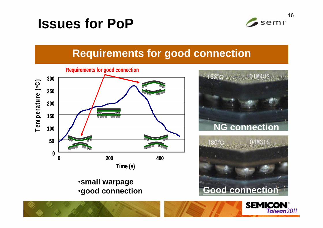
Issues for PoP
Requirements for good connection
0
50
100
150
200
250
300
0 200 400Time (s)
Tem
pera
ture
(o C)
Requirements for good connection
0
50
100
150
200
250
300
0 200 400Time (s)
Tem
pera
ture
(o C)
0
50
100
150
200
250
300
0 200 400Time (s)
Tem
pera
ture
(o C)
NG connection
Good connection•small warpage•good connection
Requirements for good connection

17
25 100 175
ThermalShrinkage
CureShrinkage
MoldShrinkage
EMC
Substrate
Temperature (ºC)
Molding
Tg
Shrin
kage
DifferentialShrinkage
Concept for reduction of warpage
Mechanism of PKG warpage
•Low CTE substrate is good to reduce warpage
Convex warpage
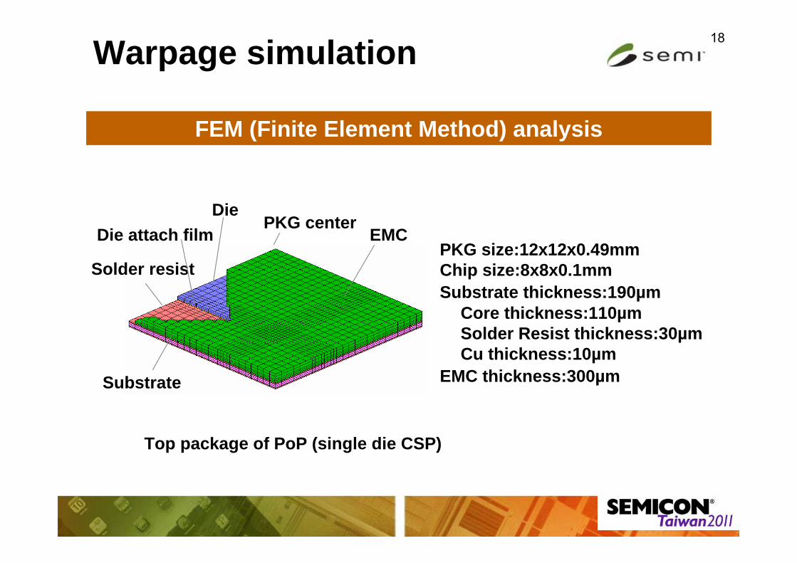
18Warpage simulation
FEM (Finite Element Method) analysis
PKG centerDie
EMC
Solder resist
Die attach film
Substrate
PKG size:12x12x0.49mmChip size:8x8x0.1mmSubstrate thickness:190µm
Core thickness:110µmSolder Resist thickness:30µmCu thickness:10µm
EMC thickness:300µm
Top package of PoP (single die CSP)
19
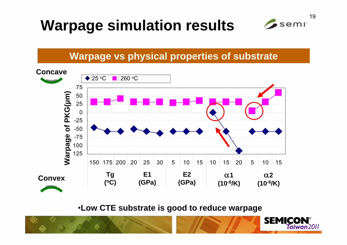
-125-100
-75-50-25
0255075
150 175 200 20 25 30 5 10 15 10 15 20 5 10 15
Tg(℃) 室温弾性率
(GPa)高温弾性率
(GPa)室温α 高温α
PKG反り(um)
◆:25 oC ■: 260 oC
Convex
Concave
Tg(oC)
E1(GPa)
E2(GPa)
1(10-6/K)
2(10-6/K)
War
page
of P
KG
(µm
)
Warpage simulation results
Warpage vs physical properties of substrate
•Low CTE substrate is good to reduce warpage
20
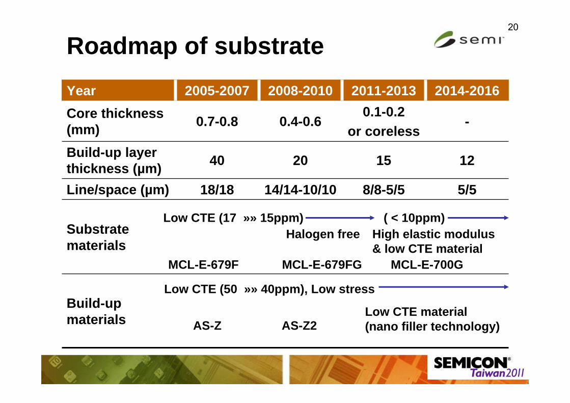
Roadmap of substrate
12152040Build-up layer thickness (µm)
5/58/8-5/514/14-10/1018/18Line/space (µm)
Build-up materials
Substrate materials
-0.1-0.2
or coreless0.4-0.60.7-0.8Core thickness
(mm)
2014-20162011-20132008-20102005-2007Year
Low CTE (17 »» 15ppm) ( < 10ppm)Halogen free
MCL-E-679F MCL-E-679FG MCL-E-700G
High elastic modulus & low CTE material
Low CTE (50 »» 40ppm), Low stress
AS-Z AS-Z2Low CTE material(nano filler technology)

21
Modulus
CTE
(ppm
/ºC)
15
10
5
Conventional laminates
Low CTE laminates
HighLow
Ultra Low CTE laminates
E-679FG
E-700G(R)
E-glass
S-glass
5ppm
2.8ppm
Concept of Ultra Low-CTE materials
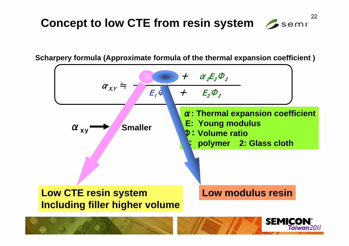
22
α2E2Φ2
E1Φ1 E2Φ2+
+α1E1Φ1
αX,Y ≒
Scharpery formula (Approximate formula of the thermal expansion coefficient )
α: Thermal expansion coefficientE: Young modulusΦ: Volume ratio1: polymer 2: Glass cloth
αxy Smaller
Low CTE resin systemIncluding filler higher volume
Low modulus resin
Concept to low CTE from resin system
23
low
C
TE
high
low Modulus high
E-679FG(R)
E-700G(R)
E-705G(LEXAM-V)E-800G
(LEXAM-X)
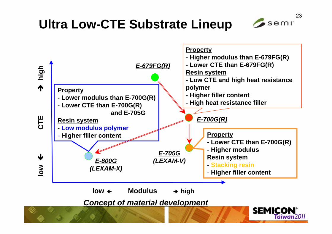
Property- Higher modulus than E-679FG(R)- Lower CTE than E-679FG(R)Resin system- Low CTE and high heat resistance polymer- Higher filler content- High heat resistance filler
Property- Lower CTE than E-700G(R)- Higher modulusResin system- Stacking resin- Higher filler content
Property- Lower modulus than E-700G(R)- Lower CTE than E-700G(R)
and E-705GResin system- Low modulus polymer- Higher filler content
Concept of material development
Ultra Low-CTE Substrate Lineup

24
Modulus
15
10
5
Conventional laminates
Low CTE laminates
HighLow
Ultra Low CTE laminates
E-glass
S-glass
5ppm
2.8ppm
E-679FG
E-700G(R)
LEXAM-VL
LEXAM-XL
Concept of Ultra Low-CTE materialsC
TE(p
pm/ºC
)

25Outline1.Trend of Semiconductor Packaging and
Technological Strategy for 3D Semiconductor Packaging Materials
2. Material Technologies • Stacked-CSP -DAF ( Die attach film)• PoP (Package on package) -Low CTE substrate • TSV (Through Silicon Via)
- Low Temperature Curable Dielectric Material- Underfill Materials (CUF, NCP, NCF)- Temporary Bonding Materials
3. Conclusion
26
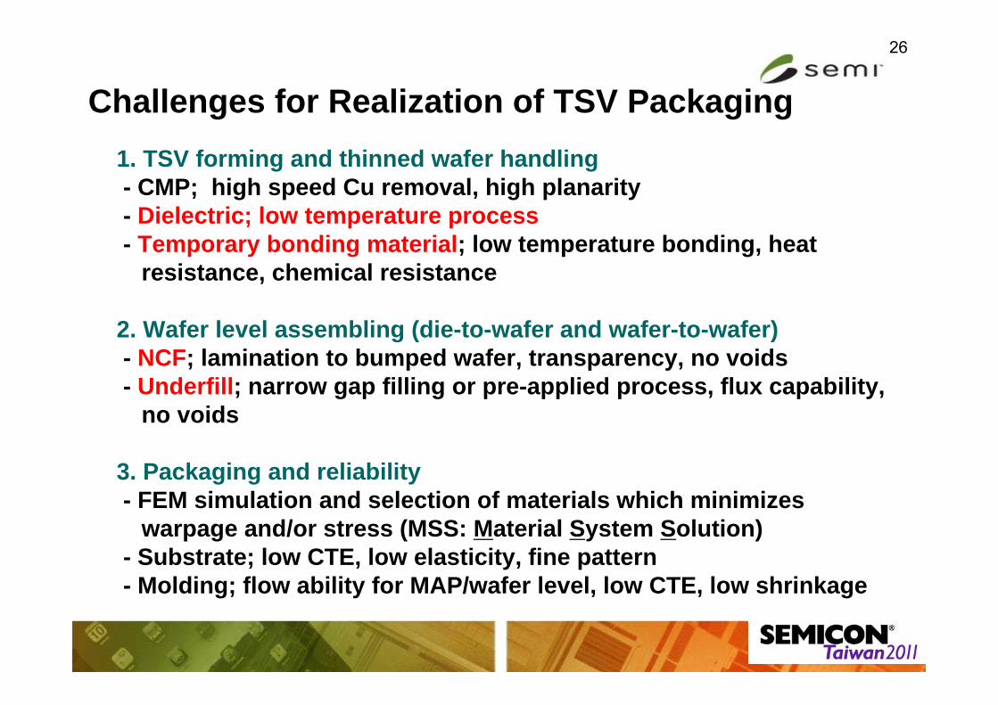
Challenges for Realization of TSV Packaging1. TSV forming and thinned wafer handling- CMP; high speed Cu removal, high planarity- Dielectric; low temperature process- Temporary bonding material; low temperature bonding, heat
resistance, chemical resistance
2. Wafer level assembling (die-to-wafer and wafer-to-wafer)- NCF; lamination to bumped wafer, transparency, no voids- Underfill; narrow gap filling or pre-applied process, flux capability,
no voids
3. Packaging and reliability- FEM simulation and selection of materials which minimizes
warpage and/or stress (MSS: Material System Solution)- Substrate; low CTE, low elasticity, fine pattern - Molding; flow ability for MAP/wafer level, low CTE, low shrinkage
27
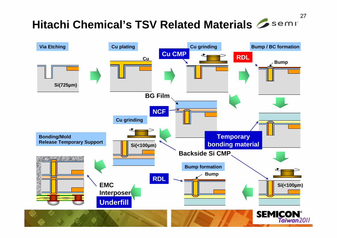
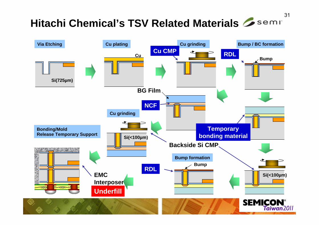
Bump / BC formationVia Etching Cu plating
Cu
Bump formationBump
Si(725µm)
Si(<100µm)
Si(<100µm)
Cu grinding
Cu grinding
Bonding/MoldRelease Temporary Support
Bump
Hitachi Chemical’s TSV Related Materials
Cu CMP RDL
Temporarybonding material
Backside Si CMP
NCF
EMCInterposerUnderfill
RDL
BG Film
28
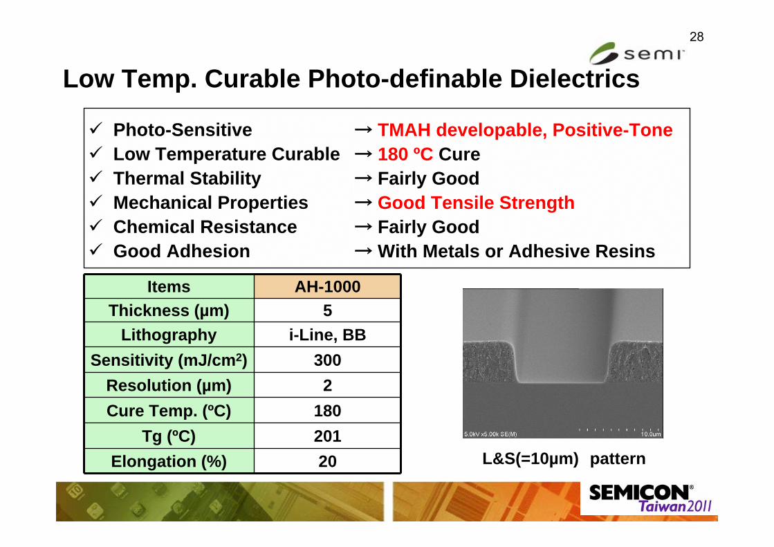
Items AH-1000Thickness (µm) 5
Lithography i-Line, BBSensitivity (mJ/cm2) 300
Resolution (µm) 2Cure Temp. (ºC) 180
Tg (ºC) 201Elongation (%) 20
Photo-Sensitive Low Temperature Curable Thermal Stability Mechanical Properties Chemical Resistance Good Adhesion
→ TMAH developable, Positive-Tone→ 180 ºC Cure→ Fairly Good→ Good Tensile Strength→ Fairly Good→ With Metals or Adhesive Resins
L&S(=10µm) pattern
Low Temp. Curable Photo-definable Dielectrics

29
Bump / BC formationVia Etching Cu plating
Cu
Bump formationBump
Si(725µm)
Si(<100µm)
Si(<100µm)
Cu grinding
Cu grinding
Bonding/MoldRelease Temporary Support
Bump
Hitachi Chemical’s TSV Related Materials
Cu CMP RDL
Temporarybonding material
Backside Si CMP
NCF
EMCInterposerUnderfill
RDL
BG Film

30
•Liquid type•Good adhesion to Si substrate•High heat resistance: Decomposition temperature > 400ºC•Removable by heat treatment: Removal temperature 230-320ºC
CuringSpin Coating
Substrate
Attachment onto Wafer
Condition : 100ºC/5min + 180ºC/30min
Wafer Thinning
Varnish
Wafer StackingSubstrate Removal
Wafer
Residual CleaningSolvent
Temp: 230-320ºCPressure : 0.5MPaTime : 5sec
Temp: 230-320ºCDirection : Horizontal
Immersion : 0.5-1.0hrSolvent temp. : R.T.
Temporary bonding materials
31
Bump / BC formationVia Etching Cu plating
Cu
Bump formationBump
Si(725µm)
Si(<100µm)
Si(<100µm)
Cu grinding
Cu grinding
Bonding/MoldRelease Temporary Support
Bump
Hitachi Chemical’s TSV Related Materials
Cu CMP RDL
Temporarybonding material
Backside Si CMP
NCF
EMCInterposerUnderfill
RDL
BG Film
32
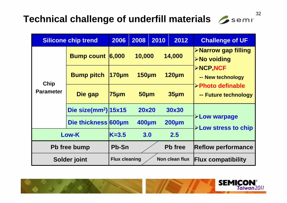
Low warpage
Low stress to chip
Narrow gap fillingNo voidingNCP,NCF
-- New technologyPhoto definable
-- Future technology
6,000 10,000 14,000Bump count
ChipParameter
Flux compatibilityFlux cleaning Non clean fluxSolder joint
Reflow performancePb-Sn Pb freePb free bump
K=3.5 3.0 2.5Low-K
600µm 400µm 200µmDie thickness
15x15 20x20 30x30Die size(mm2)
75µm 50µm 35µmDie gap
170µm 150µm 120µmBump pitch
Challenge of UF2012201020082006Silicone chip trend
Technical challenge of underfill materials
33
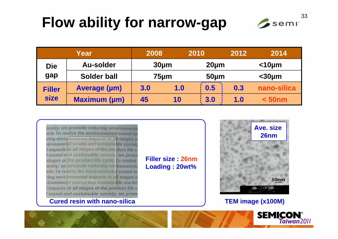
Maximum (µm)Average (µm)
Solder ballAu-solder 30µm 20µm <10µm
45 10 3.0 1.0 < 50nm3.0 1.0 0.5 0.3 nano-silicaFiller
size
75µm 50µm <30µmDie gap
2008 2010 2012 2014Year
Cured resin with nano-silica
Filler size : 26nmLoading : 20wt%
Ave. size 26nm
Flow ability for narrow-gap
TEM image (x100M)

34
Bump / BC formationVia Etching Cu plating
Cu
Bump formationBump
Si(725µm)
Si(<100µm)
Si(<100µm)
Cu grinding
Cu grinding
Bonding/MoldRelease Temporary Support
Bump
Hitachi Chemical’s TSV Related Materials
Cu CMP RDL
Temporarysupport
Backside Si CMP
NCF
EMCInterposerUnderfill
RDL
BG Film

35
6. Flip chip bonding
Substrate
1. NCF laminationonto wafer
2. Lamination of dicing tape
Bump
PETUF Film
Wafer Dicing Tape (DC)
PET
3. Wafer mount andremove cover film
4. Dicing
Wafer
Wafer Active Side
Wafer Back Side
Dicing Tape
5. Pick-up
Chip with UF Film
Process using NCF

36
Material Technologies play the important role in realizing 3D semiconductor packaging.Material system solution (MSS) has been utilized to develop new materials satisfying the requirements for 3D semiconductor packaging.
Conclusion
•Stacked-CSP- DAF for thin wafer
•PoP- Low CTE substrate; E-700G, LEXAM-series
•TSV package- Low temperature curable dielectric material-Temporary bonding material- Underfill material; CUF, pre-applied underfill; NCF, Photo definable NCF