material issues in thermal management of rf power …rf module collection of mmics and ics...
TRANSCRIPT
Material Issues in ThermalManagement of RF Power Electronics
James S. WilsonPrincipal Mechanical Engineer
Donald C. PricePrincipal Fellow
Raytheon Electronic SystemsDallas, Texas
Thermal Materials Workshop 2001Moller Centre, Churchill College
Cambridge UniversityMay 30 - June 1, 2001James Wilson
Donald [email protected]

REPORT DOCUMENTATION PAGE Form Approved OMB No.0704-0188
Public reporting burder for this collection of information is estibated to average 1 hour per response, including the time for reviewing instructions, searching existing data sources, gathering and maintaining the data needed, and completingand reviewing this collection of information. Send comments regarding this burden estimate or any other aspect of this collection of information, including suggestions for reducing this burder to Department of Defense, WashingtonHeadquarters Services, Directorate for Information Operations and Reports (0704-0188), 1215 Jefferson Davis Highway, Suite 1204, Arlington, VA 22202-4302. Respondents should be aware that notwithstanding any other provision oflaw, no person shall be subject to any penalty for failing to comply with a collection of information if it does not display a currently valid OMB control number. PLEASE DO NOT RETURN YOUR FORM TO THE ABOVE ADDRESS.
1. REPORT DATE (DD-MM-YYYY)30-05-2001
2. REPORT TYPEWorkshop Presentations
3. DATES COVERED (FROM - TO)30-05-2001 to 01-06-2001
4. TITLE AND SUBTITLEMaterial Issues in Thermal Management of RF Power ElectronicsUnclassified
5a. CONTRACT NUMBER5b. GRANT NUMBER5c. PROGRAM ELEMENT NUMBER
6. AUTHOR(S)Wilson, James S. ;Price, Donald C. ;
5d. PROJECT NUMBER5e. TASK NUMBER5f. WORK UNIT NUMBER
7. PERFORMING ORGANIZATION NAME AND ADDRESSRaytheon Electronic SystemsDallas, TXxxxxx
8. PERFORMING ORGANIZATION REPORTNUMBER
9. SPONSORING/MONITORING AGENCY NAME AND ADDRESSOffice of Naval Research International Field OfficeOffice of Naval ResearchWashington, DCxxxxx
10. SPONSOR/MONITOR'S ACRONYM(S)11. SPONSOR/MONITOR'S REPORTNUMBER(S)
12. DISTRIBUTION/AVAILABILITY STATEMENTAPUBLIC RELEASE,13. SUPPLEMENTARY NOTESSee Also ADM001348, Thermal Materials Workshop 2001, held in Cambridge, UK on May 30-June 1, 2001. Additional papers can bedownloaded from: http://www-mech.eng.cam.ac.uk/onr/14. ABSTRACT? System Level ? Description of system(s) ? Thermal management issues ? Temperature gradients ? Absolute temperature levels ? Specialarray-level (AESA) problems ? Role of materials at the system level ? Component Level ? Primary source of thermal dissipation ? Uniquethermal analysis aspects of RF components ? Role of materials at the component level15. SUBJECT TERMS16. SECURITY CLASSIFICATION OF: 17. LIMITATION
OF ABSTRACTPublic Release
18.NUMBEROF PAGES31
19. NAME OF RESPONSIBLE PERSONFenster, [email protected]
a. REPORTUnclassified
b. ABSTRACTUnclassified
c. THIS PAGEUnclassified
19b. TELEPHONE NUMBERInternational Area CodeArea Code Telephone Number703767-9007DSN427-9007
Standard Form 298 (Rev. 8-98)Prescribed by ANSI Std Z39.18
Thermal Materials Workshop 2001 - Cambridge University 2
Introduction
• System Level– Description of system(s)– Thermal management issues
• Temperature gradients• Absolute temperature levels• Special array-level (AESA) problems
– Role of materials at the system level• Component Level
– Primary source of thermal dissipation– Unique thermal analysis aspects of RF components– Role of materials at the component level

Thermal Materials Workshop 2001 - Cambridge University 3
Phased Array System Hierarchy
Phased arrayhierarchy
Physicaldimensions,characteristics
Materialissues
Thermalmanagementissues
Active antenna Meters, manyelements
StructuralsupportThermalgradient
Coolant routingHeatabsorption
Slat, Subpanel Meterseveralelements
Interconnect,CTE, thermal
Packagingdensity
RF Module Collection ofMMICs and ICs
Dielectric,CTE, thermal,hermetic
Module attachthermalinterface
Device PowerAmplifiers sub-micron activearea
SemiconductorThermalinterfaces
Die attachFET layout

Thermal Materials Workshop 2001 - Cambridge University 4
Typical RF Platforms / SystemsAirborne and Ground Systems
• Often require designs for continuous operation
Ground based
Airborne
Shipborne

Thermal Materials Workshop 2001 - Cambridge University 5
Typical RF Platforms / Systems Satellite Systems
• Large antenna dimensions• May have thousands of modules• May have option of intermittent or short term operation
Modules
MMICsPower Converter

Thermal Materials Workshop 2001 - Cambridge University 6
Typical RF Platforms / Systems Phased-Array Radars
Active Array Subarray (Slat)
Modules
MMICsPower Converter
• Phased-array radars typically operate at frequencies from1 to 30 GHz and dissipate from hundreds to tens of thousandsof KW of waste heat
• Phased-array radars often contain many thousands of microwavemodules as building blocks for AESA (Active Electronically SteeredArrays)
• Power dissipations of ground-based systems are typically higher thanairborne systems because of physical size, but dissipation flux levelsare comparable
Thermal Materials Workshop 2001 - Cambridge University 7
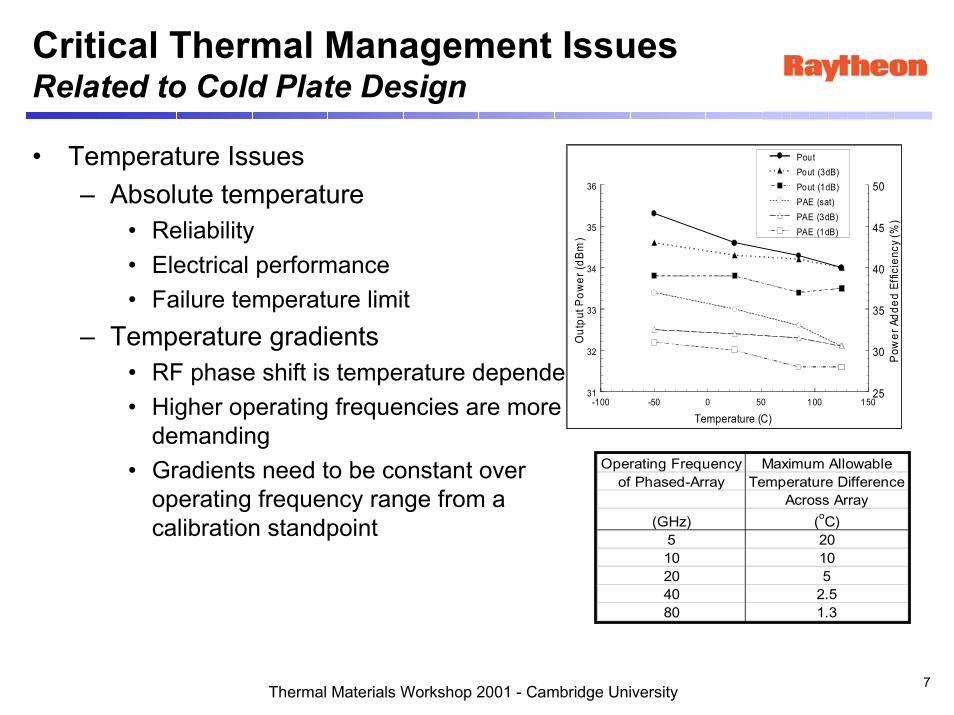
Critical Thermal Management IssuesRelated to Cold Plate Design
• Temperature Issues– Absolute temperature
• Reliability• Electrical performance• Failure temperature limit
– Temperature gradients• RF phase shift is temperature dependent• Higher operating frequencies are more
demanding• Gradients need to be constant over
operating frequency range from acalibration standpoint
Operating Frequency Maximum Allowableof Phased-Array Temperature Difference
Across Array(GHz) (oC)
5 2010 1020 540 2.580 1.3
-100 -50 0 50 100 150
Temperature (C)
31
32
33
34
35
36
Out
put P
ower
(dBm
)
25
30
35
40
45
50
Pow
er A
dded
Effi
cien
cy (%
)
PoutPout (3dB)Pout (1dB)PAE (sat)PAE (3dB)PAE (1dB)

Thermal Materials Workshop 2001 - Cambridge University 8
Reliability IssueRequires Use of Channel Temperature
Same data plotted considering either base or channel temperature
Thermal Materials Workshop 2001 - Cambridge University 9
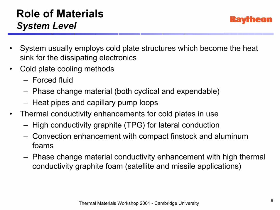
Role of MaterialsSystem Level
• System usually employs cold plate structures which become the heatsink for the dissipating electronics
• Cold plate cooling methods– Forced fluid– Phase change material (both cyclical and expendable)– Heat pipes and capillary pump loops
• Thermal conductivity enhancements for cold plates in use– High conductivity graphite (TPG) for lateral conduction– Convection enhancement with compact finstock and aluminum
foams– Phase change material conductivity enhancement with high thermal
conductivity graphite foam (satellite and missile applications)
Thermal Materials Workshop 2001 - Cambridge University 10
Role of MaterialsSystem Level (continued)
• Wide environmental operating range requires that coefficient ofthermal expansion (CTE) differences be addressed– RF electronic package materials are set and not likely to change– Constrain the cold plates
• Aluminum Silicon Carbide cold plates provide good match– Compliant bonds
• Thermal concerns (this is often the weak link in the thermaldesign)
• Good for repairability concerns• Material compatibility (from the standpoint of galvanic corrosion)
must also be considered– Long shelf life required– Usually solved by metal plating

Thermal Materials Workshop 2001 - Cambridge University 11
Power Dissipation and Heat Flux Issues
TypicalDissipation
(Watts)
Typical HeatFlux
(W/cm2)
FET 1 to 15 Order of 1E7 atjunction
MMICSeveral FETs
1 to 20 100 - 2000(at base MMIC)
Module(severalMMICs)
1 to 50 1 to 5
Coldplate(severalmodules)
10 to 2000 0.5 to 3
System(severalcoldplates)
100 to many kW Order of 1
Concentrated heat fluxat device junction

Thermal Materials Workshop 2001 - Cambridge University 12
OutlineTR Module and MMIC Thermal Issues
• TR Module and MMICs– Description
• Materials– Analysis
• Specialized techniques• Examples
– Verification• IR imaging
Thermal Materials Workshop 2001 - Cambridge University 13
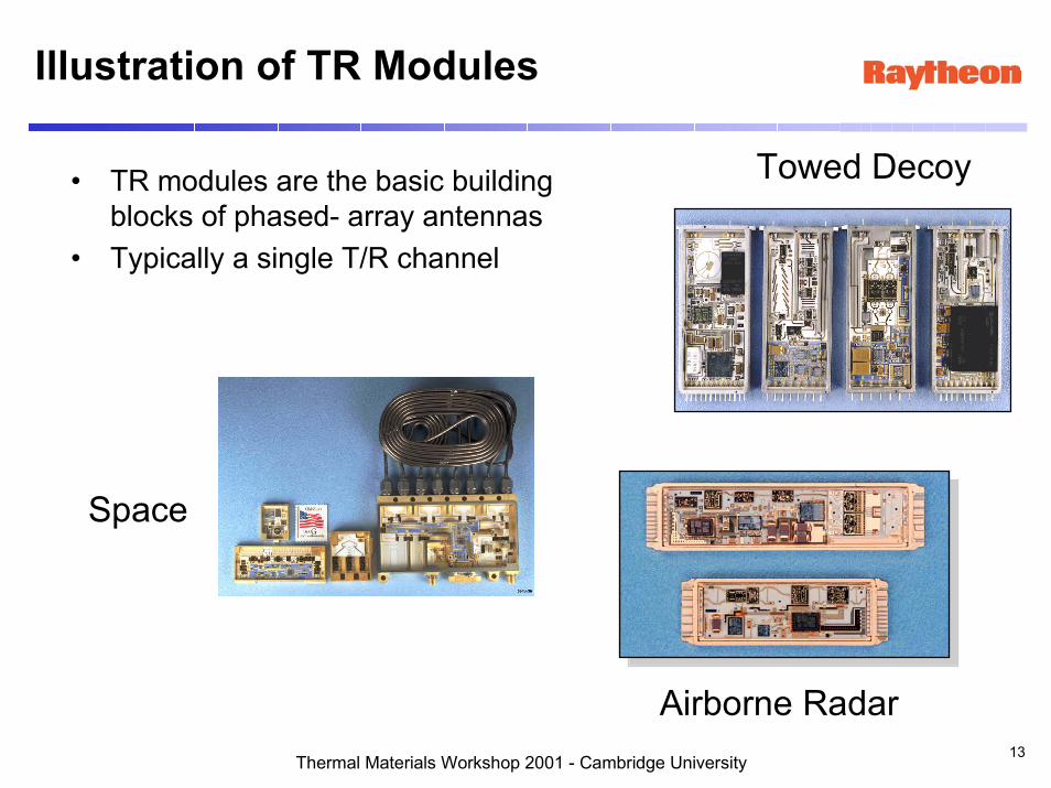
Illustration of TR Modules
• TR modules are the basic buildingblocks of phased- array antennas
• Typically a single T/R channel
Space
Airborne Radar
Towed Decoy
Thermal Materials Workshop 2001 - Cambridge University 14
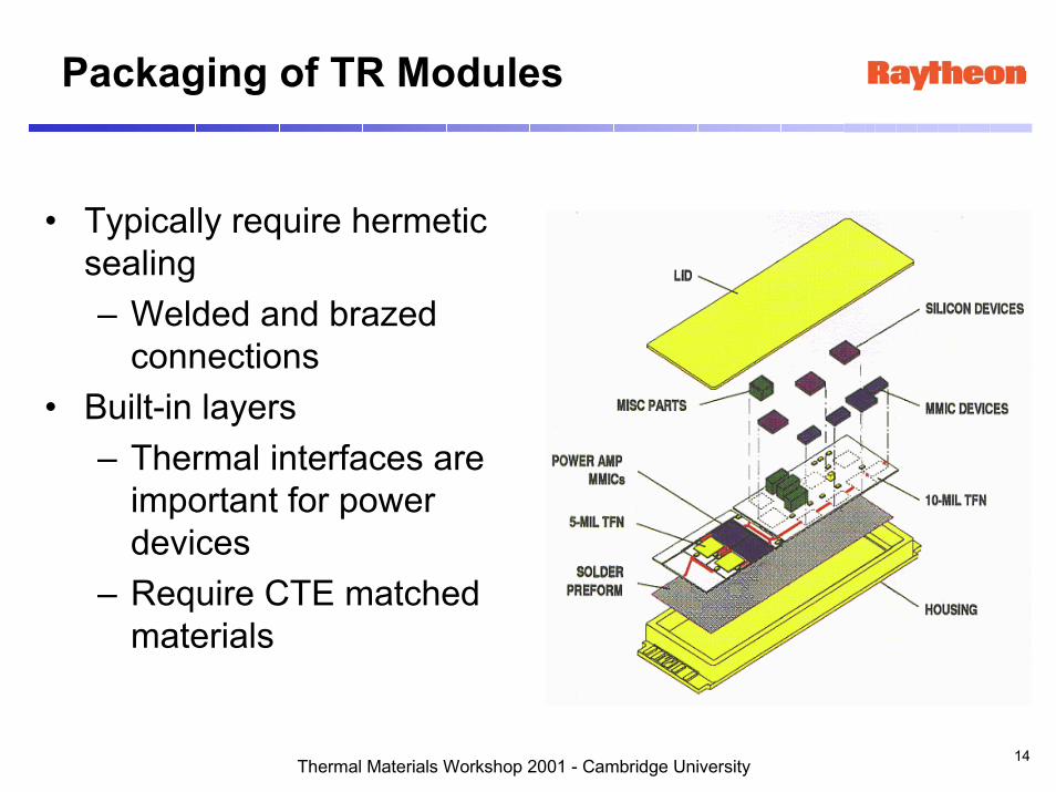
• Typically require hermeticsealing– Welded and brazed
connections• Built-in layers
– Thermal interfaces areimportant for powerdevices
– Require CTE matchedmaterials
Packaging of TR Modules
Thermal Materials Workshop 2001 - Cambridge University 15
Role of MaterialsPackage Level
• Dielectric substrates– Al2O3, BeO, AlN, thick film, some circuit board
• Heat spreaders for MMICs/Module base– Copper Moly, Copper Tungsten, Diamond, Molybdenum,
Kovar, Titanium• Die attach
– Solders (AuSn, SnPb, Indium)– Silver-filled epoxy– Z-axis material and solders for flip chip
• Module attach– Compliant adhesives, filled epoxies, metal-metal– Ball grid array

Thermal Materials Workshop 2001 - Cambridge University 16
Module/MMIC Thermal AnalysisRequirements for Numerical Solution
• Numerically difficult– Large scale range– Non-linear material properties (GaAs, GaN, SiC, BeO)– Fully three-dimensional– Pulsed operation (transient analysis required)
• Often a majority of the total temperature rise from thejunction to sink is in the module and MMIC– Thermal design of module/MMIC most important from
an ambient-to-junction temperature rise perspective

Thermal Materials Workshop 2001 - Cambridge University 17
Transition From System To Device
Antenna Level• Orbit environment
or system levelanalysis
• Provide boundarycondition for modulemodel
• Time scale in minutes
Module Level• Boundary condition
from antenna model• Predict module base
temperature foroperating conditions
• Time scale in seconds
MMIC Level• Boundary condition
from module model• Junction temperature
prediction• Time scale in
microseconds
T/R ModuleIREarth IR Solar
Antenna model
GaAsEpoxyAlSiC
Surface MetalBoundary Condition

Thermal Materials Workshop 2001 - Cambridge University 18
Scale VariationMMICs and Microwave Modules
Thermal Materials Workshop 2001 - Cambridge University 19
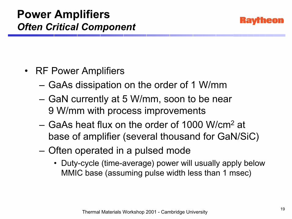
Power AmplifiersOften Critical Component
• RF Power Amplifiers– GaAs dissipation on the order of 1 W/mm– GaN currently at 5 W/mm, soon to be near
9 W/mm with process improvements– GaAs heat flux on the order of 1000 W/cm2 at
base of amplifier (several thousand for GaN/SiC)– Often operated in a pulsed mode
• Duty-cycle (time-average) power will usually apply belowMMIC base (assuming pulse width less than 1 msec)
Thermal Materials Workshop 2001 - Cambridge University 20
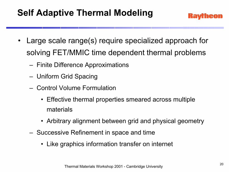
Self Adaptive Thermal Modeling
• Large scale range(s) require specialized approach forsolving FET/MMIC time dependent thermal problems– Finite Difference Approximations
– Uniform Grid Spacing
– Control Volume Formulation
• Effective thermal properties smeared across multiplematerials
• Arbitrary alignment between grid and physical geometry
– Successive Refinement in space and time
• Like graphics information transfer on internet

Thermal Materials Workshop 2001 - Cambridge University 21
Steady-State Nesting

Thermal Materials Workshop 2001 - Cambridge University 22
Transient Nesting
Solutioncomputationaltimes at least twoorders ofmagnitude fasterthan commercialtools
Thermal Materials Workshop 2001 - Cambridge University 23
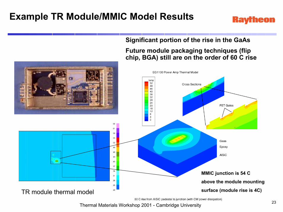
Example TR Module/MMIC Model Results
TR module thermal model
Significant portion of the rise in the GaAsFuture module packaging techniques (flipchip, BGA) still are on the order of 60 C rise
MMIC junction is 54 C
above the module mounting
surface (module rise is 4C)
Thermal Materials Workshop 2001 - Cambridge University 24
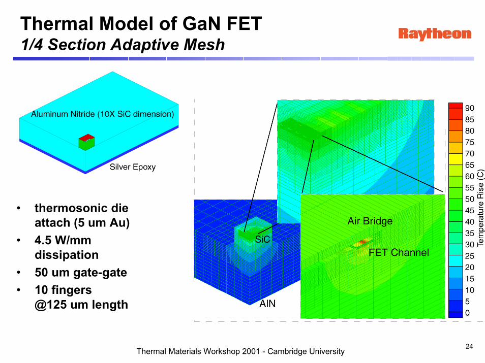
Thermal Model of GaN FET1/4 Section Adaptive Mesh
• thermosonic dieattach (5 um Au)
• 4.5 W/mmdissipation
• 50 um gate-gate• 10 fingers
@125 um length

Thermal Materials Workshop 2001 - Cambridge University 25
Package Materials /TradesDiamond Heat Spreader
Evaluations at 4.5 W/mm dissipation
Benefit with diamond for MMICs but not for discrete FETs
SiC Thk(microns)
Diamondarea
TemperatureRise (C)
Comparison case toone AuSn layer and
same SiC thickness -no diamond
ThickDiscrete
425 same asSiC
91.4 89.3
ThinDiscrete
125 same asSiC
84.3 85.0
ThickMMIC
425 same asAlN
80.0 89.3
ThinMMIC
125 same asAlN
72.9 85.0

Thermal Materials Workshop 2001 - Cambridge University 26
GaN FET Channel Spacing Trade
Rapid thermal analysiscapability allowsdesign trades prior todevice fabrication
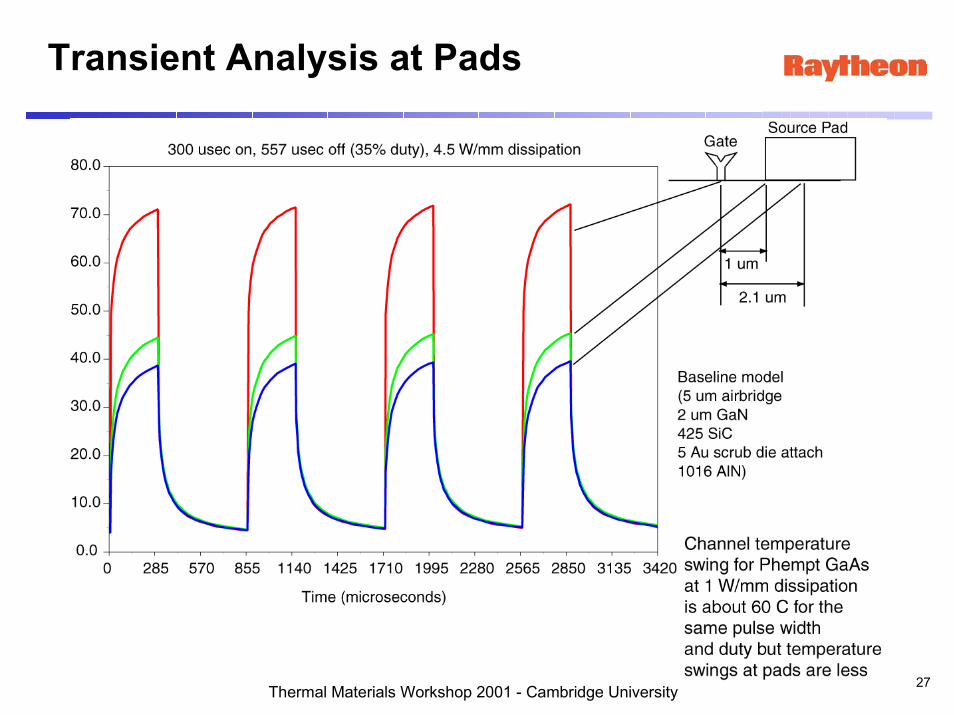
Thermal Materials Workshop 2001 - Cambridge University 27
Transient Analysis at Pads
Thermal Materials Workshop 2001 - Cambridge University 28
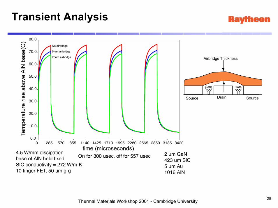
Transient Analysis

Thermal Materials Workshop 2001 - Cambridge University 29
Model Verification with IR
IR at 10 �m resolution
Test: 106 C rise
Model: 102 C rise
Thermal Materials Workshop 2001 - Cambridge University 30
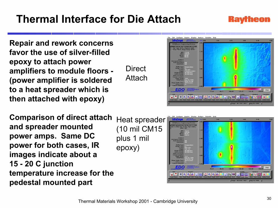
Direct Attach
Heat spreader(10 mil CM15plus 1 milepoxy)
Repair and rework concernsfavor the use of silver-filledepoxy to attach poweramplifiers to module floors -(power amplifier is solderedto a heat spreader which isthen attached with epoxy)
Comparison of direct attachand spreader mountedpower amps. Same DCpower for both cases, IRimages indicate about a15 - 20 C junctiontemperature increase for thepedestal mounted part
Thermal Interface for Die Attach
Thermal Materials Workshop 2001 - Cambridge University 31
Conclusions
• Material interface issues very important– Module and die attach (heat flux high)– Compliant attach may be required because of
CTE concerns• Thermal analysis needs to be integrated into the
power amplifier design process• Material properties for “thin film” materials at device
level are not well known (surface metalization)